WO2012128074A1 - 照明装置、表示装置、及びテレビ受信装置 - Google Patents
照明装置、表示装置、及びテレビ受信装置 Download PDFInfo
- Publication number
- WO2012128074A1 WO2012128074A1 PCT/JP2012/056097 JP2012056097W WO2012128074A1 WO 2012128074 A1 WO2012128074 A1 WO 2012128074A1 JP 2012056097 W JP2012056097 W JP 2012056097W WO 2012128074 A1 WO2012128074 A1 WO 2012128074A1
- Authority
- WO
- WIPO (PCT)
- Prior art keywords
- wiring
- light source
- led
- positive
- negative
- Prior art date
- Legal status (The legal status is an assumption and is not a legal conclusion. Google has not performed a legal analysis and makes no representation as to the accuracy of the status listed.)
- Ceased
Links
Images












Classifications
-
- G—PHYSICS
- G02—OPTICS
- G02F—OPTICAL DEVICES OR ARRANGEMENTS FOR THE CONTROL OF LIGHT BY MODIFICATION OF THE OPTICAL PROPERTIES OF THE MEDIA OF THE ELEMENTS INVOLVED THEREIN; NON-LINEAR OPTICS; FREQUENCY-CHANGING OF LIGHT; OPTICAL LOGIC ELEMENTS; OPTICAL ANALOGUE/DIGITAL CONVERTERS
- G02F1/00—Devices or arrangements for the control of the intensity, colour, phase, polarisation or direction of light arriving from an independent light source, e.g. switching, gating or modulating; Non-linear optics
- G02F1/01—Devices or arrangements for the control of the intensity, colour, phase, polarisation or direction of light arriving from an independent light source, e.g. switching, gating or modulating; Non-linear optics for the control of the intensity, phase, polarisation or colour
- G02F1/13—Devices or arrangements for the control of the intensity, colour, phase, polarisation or direction of light arriving from an independent light source, e.g. switching, gating or modulating; Non-linear optics for the control of the intensity, phase, polarisation or colour based on liquid crystals, e.g. single liquid crystal display cells
- G02F1/133—Constructional arrangements; Operation of liquid crystal cells; Circuit arrangements
- G02F1/1333—Constructional arrangements; Manufacturing methods
- G02F1/1335—Structural association of cells with optical devices, e.g. polarisers or reflectors
- G02F1/1336—Illuminating devices
- G02F1/133602—Direct backlight
- G02F1/133603—Direct backlight with LEDs
-
- G—PHYSICS
- G02—OPTICS
- G02F—OPTICAL DEVICES OR ARRANGEMENTS FOR THE CONTROL OF LIGHT BY MODIFICATION OF THE OPTICAL PROPERTIES OF THE MEDIA OF THE ELEMENTS INVOLVED THEREIN; NON-LINEAR OPTICS; FREQUENCY-CHANGING OF LIGHT; OPTICAL LOGIC ELEMENTS; OPTICAL ANALOGUE/DIGITAL CONVERTERS
- G02F1/00—Devices or arrangements for the control of the intensity, colour, phase, polarisation or direction of light arriving from an independent light source, e.g. switching, gating or modulating; Non-linear optics
- G02F1/01—Devices or arrangements for the control of the intensity, colour, phase, polarisation or direction of light arriving from an independent light source, e.g. switching, gating or modulating; Non-linear optics for the control of the intensity, phase, polarisation or colour
- G02F1/13—Devices or arrangements for the control of the intensity, colour, phase, polarisation or direction of light arriving from an independent light source, e.g. switching, gating or modulating; Non-linear optics for the control of the intensity, phase, polarisation or colour based on liquid crystals, e.g. single liquid crystal display cells
- G02F1/133—Constructional arrangements; Operation of liquid crystal cells; Circuit arrangements
- G02F1/1333—Constructional arrangements; Manufacturing methods
- G02F1/1335—Structural association of cells with optical devices, e.g. polarisers or reflectors
- G02F1/1336—Illuminating devices
- G02F1/133602—Direct backlight
- G02F1/133606—Direct backlight including a specially adapted diffusing, scattering or light controlling members
- G02F1/133607—Direct backlight including a specially adapted diffusing, scattering or light controlling members the light controlling member including light directing or refracting elements, e.g. prisms or lenses
-
- G—PHYSICS
- G02—OPTICS
- G02F—OPTICAL DEVICES OR ARRANGEMENTS FOR THE CONTROL OF LIGHT BY MODIFICATION OF THE OPTICAL PROPERTIES OF THE MEDIA OF THE ELEMENTS INVOLVED THEREIN; NON-LINEAR OPTICS; FREQUENCY-CHANGING OF LIGHT; OPTICAL LOGIC ELEMENTS; OPTICAL ANALOGUE/DIGITAL CONVERTERS
- G02F1/00—Devices or arrangements for the control of the intensity, colour, phase, polarisation or direction of light arriving from an independent light source, e.g. switching, gating or modulating; Non-linear optics
- G02F1/01—Devices or arrangements for the control of the intensity, colour, phase, polarisation or direction of light arriving from an independent light source, e.g. switching, gating or modulating; Non-linear optics for the control of the intensity, phase, polarisation or colour
- G02F1/13—Devices or arrangements for the control of the intensity, colour, phase, polarisation or direction of light arriving from an independent light source, e.g. switching, gating or modulating; Non-linear optics for the control of the intensity, phase, polarisation or colour based on liquid crystals, e.g. single liquid crystal display cells
- G02F1/133—Constructional arrangements; Operation of liquid crystal cells; Circuit arrangements
- G02F1/1333—Constructional arrangements; Manufacturing methods
- G02F1/1335—Structural association of cells with optical devices, e.g. polarisers or reflectors
- G02F1/1336—Illuminating devices
- G02F1/133602—Direct backlight
- G02F1/133608—Direct backlight including particular frames or supporting means
-
- G—PHYSICS
- G02—OPTICS
- G02F—OPTICAL DEVICES OR ARRANGEMENTS FOR THE CONTROL OF LIGHT BY MODIFICATION OF THE OPTICAL PROPERTIES OF THE MEDIA OF THE ELEMENTS INVOLVED THEREIN; NON-LINEAR OPTICS; FREQUENCY-CHANGING OF LIGHT; OPTICAL LOGIC ELEMENTS; OPTICAL ANALOGUE/DIGITAL CONVERTERS
- G02F1/00—Devices or arrangements for the control of the intensity, colour, phase, polarisation or direction of light arriving from an independent light source, e.g. switching, gating or modulating; Non-linear optics
- G02F1/01—Devices or arrangements for the control of the intensity, colour, phase, polarisation or direction of light arriving from an independent light source, e.g. switching, gating or modulating; Non-linear optics for the control of the intensity, phase, polarisation or colour
- G02F1/13—Devices or arrangements for the control of the intensity, colour, phase, polarisation or direction of light arriving from an independent light source, e.g. switching, gating or modulating; Non-linear optics for the control of the intensity, phase, polarisation or colour based on liquid crystals, e.g. single liquid crystal display cells
- G02F1/133—Constructional arrangements; Operation of liquid crystal cells; Circuit arrangements
- G02F1/1333—Constructional arrangements; Manufacturing methods
- G02F1/1335—Structural association of cells with optical devices, e.g. polarisers or reflectors
- G02F1/1336—Illuminating devices
- G02F1/133602—Direct backlight
- G02F1/133612—Electrical details
-
- G—PHYSICS
- G02—OPTICS
- G02F—OPTICAL DEVICES OR ARRANGEMENTS FOR THE CONTROL OF LIGHT BY MODIFICATION OF THE OPTICAL PROPERTIES OF THE MEDIA OF THE ELEMENTS INVOLVED THEREIN; NON-LINEAR OPTICS; FREQUENCY-CHANGING OF LIGHT; OPTICAL LOGIC ELEMENTS; OPTICAL ANALOGUE/DIGITAL CONVERTERS
- G02F1/00—Devices or arrangements for the control of the intensity, colour, phase, polarisation or direction of light arriving from an independent light source, e.g. switching, gating or modulating; Non-linear optics
- G02F1/01—Devices or arrangements for the control of the intensity, colour, phase, polarisation or direction of light arriving from an independent light source, e.g. switching, gating or modulating; Non-linear optics for the control of the intensity, phase, polarisation or colour
- G02F1/13—Devices or arrangements for the control of the intensity, colour, phase, polarisation or direction of light arriving from an independent light source, e.g. switching, gating or modulating; Non-linear optics for the control of the intensity, phase, polarisation or colour based on liquid crystals, e.g. single liquid crystal display cells
- G02F1/133—Constructional arrangements; Operation of liquid crystal cells; Circuit arrangements
- G02F1/136—Liquid crystal cells structurally associated with a semi-conducting layer or substrate, e.g. cells forming part of an integrated circuit
- G02F1/1362—Active matrix addressed cells
- G02F1/13624—Active matrix addressed cells having more than one switching element per pixel
-
- G—PHYSICS
- G02—OPTICS
- G02F—OPTICAL DEVICES OR ARRANGEMENTS FOR THE CONTROL OF LIGHT BY MODIFICATION OF THE OPTICAL PROPERTIES OF THE MEDIA OF THE ELEMENTS INVOLVED THEREIN; NON-LINEAR OPTICS; FREQUENCY-CHANGING OF LIGHT; OPTICAL LOGIC ELEMENTS; OPTICAL ANALOGUE/DIGITAL CONVERTERS
- G02F2201/00—Constructional arrangements not provided for in groups G02F1/00 - G02F7/00
- G02F2201/46—Fixing elements
- G02F2201/465—Snap -fit
-
- G—PHYSICS
- G02—OPTICS
- G02F—OPTICAL DEVICES OR ARRANGEMENTS FOR THE CONTROL OF LIGHT BY MODIFICATION OF THE OPTICAL PROPERTIES OF THE MEDIA OF THE ELEMENTS INVOLVED THEREIN; NON-LINEAR OPTICS; FREQUENCY-CHANGING OF LIGHT; OPTICAL LOGIC ELEMENTS; OPTICAL ANALOGUE/DIGITAL CONVERTERS
- G02F2201/00—Constructional arrangements not provided for in groups G02F1/00 - G02F7/00
- G02F2201/52—RGB geometrical arrangements
Definitions
- the present invention relates to a lighting device, a display device, and a television receiver.
- a backlight device is separately required as a lighting device.
- the backlight device is installed on the back side of the liquid crystal panel (the side opposite to the display surface).
- the liquid crystal panel side surface is open, a light source accommodated in the chassis, a light source, And an optical member (such as a diffusion sheet) that is disposed so as to cover the opening of the chassis so as to be opposed to efficiently emit light emitted from the light source to the liquid crystal panel side.
- an LED may be used as a light source.
- an LED substrate on which the LED is mounted is accommodated in the chassis.
- what was described in following patent document 1 is known as an example of the backlight apparatus which used LED as a light source.
- the present invention has been completed based on the above-described circumstances, and it is an object of the present invention to prevent unevenness in luminance, to improve workability related to assembly, and to reduce manufacturing costs.
- a power supply board capable of supplying power, a positive-side wiring whose one end is connected to the power-supply board, and a light source are mounted, and the other end of the positive-side wiring is connected.
- the other end side is connected to the negative light source substrate on the side light source substrate, thereby providing relay wiring for relaying power supply from the positive light source substrate side to the negative light source substrate side.
- the positive-side light source substrate and the negative-side light source substrate are electrically connected to the power source substrate by the positive-side wiring, the relay wiring, and the negative-side wiring, so that the light source mounted on each light source substrate Electric power can be supplied.
- a relay wiring for example, a relay connector is temporarily mounted on each of the positive-side light source substrate and the negative-side light source substrate, and the relay connectors mutually A connection structure that does not require a relay connector as in the case of connecting the cables can be realized. Since this kind of relay connector can be a dark part in the illumination device, according to the present invention, it is possible to make it difficult to generate a dark part.
- the positive-side light source substrate and the negative-side light source substrate are connected by the relay wiring, for example, when each light source substrate is individually connected to the power supply substrate, for each light source substrate Compared with the need for the positive electrode side wiring and the negative electrode side wiring, it is possible to reduce the number of wirings connecting the power supply substrate and each light source substrate and to shorten the entire wiring length. Thereby, the workability related to assembly can be improved, and the cost related to manufacturing can be reduced.
- a chassis in which the positive-side light source substrate and the negative-side light source substrate are accommodated is provided, and the positive-side wiring, the negative-side wiring, and the relay wiring are arranged on an outer edge portion of the chassis.
- the positive-side wiring, the negative-side wiring, and the relay wiring connected to the positive-side light source substrate and negative-side light source substrate housed in the chassis are arranged on the outer edge portion of the chassis. It becomes difficult to be done.
- the chassis includes a bottom plate that receives the positive-side light source substrate and the negative-side light source substrate, and the bottom plate includes a surface on which the positive-side light source substrate and the negative-side light source substrate are disposed.
- the power supply substrate is attached to the opposite surface, and a wiring insertion hole for passing the positive side wiring and the negative side wiring is formed therethrough. If it does in this way, each light source board and power supply board which are arranged on the other side across the bottom plate will be connected to each other by the positive side wiring and the negative side wiring which are passed through the wiring insertion hole which penetrates the bottom plate. .
- a wiring protection member is attached to the bottom plate so as to surround the hole edge of the wiring insertion hole. In this way, it is possible to prevent the positive electrode side wiring and the negative electrode side wiring from directly interfering with the hole edge of the wiring insertion hole in the bottom plate by the wiring protection member, so that it is possible to prevent disconnection of each wiring. Therefore, connection reliability is excellent.
- the wiring insertion hole is composed of at least two of the one through which the positive electrode side wiring is passed and the one through which the negative electrode side wiring is passed.
- a dedicated wiring insertion hole through which the positive electrode side wiring is passed and a dedicated wiring insertion hole through which the negative electrode side wiring is passed are included, so the positive electrode side wiring and the negative electrode side wiring are distinguished from each other. It becomes easy to attach and contributes to the improvement of workability. And since the freedom degree of arrangement
- a chassis that accommodates the positive-side light source substrate and the negative-side light source substrate is provided, and the chassis covers the positive-side light source substrate and the negative-side light source substrate while passing the light source.
- a reflecting member that reflects light from the light source to the light emitting side is provided, and the reflecting member is arranged to cover the positive electrode side wiring, the negative electrode side wiring, and the relay wiring.
- the positive electrode side wiring, the negative electrode side wiring, and the relay wiring each have a different color on the surface. In this way, when performing the connection work of each wiring, the type of each wiring can be easily identified, so that the workability related to the connection can be further improved.
- the positive electrode side light source substrate and the negative electrode side light source substrate are arranged adjacent to each other to form a set, and in addition to the plurality of sets arranged in parallel in a row, the positive electrode side Wiring, the negative electrode side wiring, and the relay wiring are provided in the same number as the number of sets of the positive electrode side light source substrate and the negative electrode side light source substrate, and the positive electrode side wiring, the negative electrode side wiring, and the relay wiring are Of the set of the positive-side light source substrate and the negative-electrode side light source substrate, the surface connected to the odd-numbered one and the one connected to the even-numbered one in the parallel direction have different colors on the surface. It is supposed to be.
- Each of the positive-side light source substrate and the negative-side light source substrate is provided with a wiring pattern in which a plurality of the light sources are mounted and the plurality of light sources are connected in series.
- One side is connected to the positive electrode side wiring or the relay wiring, and the other end side is connected to the relay wiring or the negative electrode side wiring.
- the positive-side light source substrate one end of the wiring pattern is connected to the positive-side wiring, and the other end is connected to the relay wiring, so that power is supplied to the plurality of mounted light sources.
- the negative electrode side light source substrate power is supplied to a plurality of mounted light sources by connecting one end side of the wiring pattern to the relay wiring and the other end side to the negative electrode side wiring. This is suitable when a large number of light sources are required, and is particularly useful when the lighting device is enlarged.
- the relay wiring is composed of a plurality of divided relay wirings, and one end side of the plurality of divided relay wirings is on the positive electrode side
- the other end side of the light source board is connected to the intermediate light source board so that the power supply is relayed from the positive light source board side to the intermediate light source board side, and one end side is connected to the intermediate light source board and the other end side.
- the intermediate light source substrate disposed between the positive-side light source substrate connected to the positive-side wiring and the negative-side light source substrate connected to the negative-side wiring is provided with a plurality of divided relay wires.
- this intermediate light source substrate is connected to the power supply substrate by the positive electrode side wiring and the negative electrode side wiring different from those connected to the positive electrode side light source substrate and the negative electrode side light source substrate because electric power can be supplied.
- the number of wirings connecting the power supply substrate and each light source substrate can be further reduced.
- the divided relay wiring is different from the intermediate light source board having one end side connected to the intermediate light source board and the other end side connected to the one end side. Those connected to the light source substrate are included. In this way, power can be supplied to the plurality of intermediate light source substrates, so that the number of wirings connecting the power supply substrate and each light source substrate can be further reduced.
- a display device of the present invention includes the above-described illumination device and a display panel that performs display using light from the illumination device.
- the illumination device that supplies light to the display panel is less likely to cause luminance unevenness, and can improve the workability related to assembly and reduce the manufacturing cost. High display quality can be obtained, and excellent workability and cost can be achieved.
- a liquid crystal panel can be exemplified as the display panel.
- Such a display device can be applied as a liquid crystal display device to various uses such as a display of a television or a personal computer, and is particularly suitable for a large screen.
- FIG. 1 is an exploded perspective view showing a schematic configuration of a television receiver according to Embodiment 1 of the present invention.
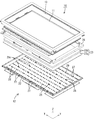
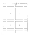
- Exploded perspective view showing schematic configuration of liquid crystal display device Sectional drawing which shows the cross-sectional structure along the long side direction of a liquid crystal panel Enlarged plan view showing the planar configuration of the array substrate Enlarged plan view showing the planar configuration of the CF substrate
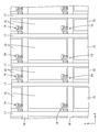
- the top view which shows arrangement
- Sectional drawing which shows the cross-sectional structure along the short side direction (vii-vii line of FIG.
- FIG. 6 Sectional drawing which shows the cross-sectional structure along the long side direction (viii-viii line of FIG. 6) of a liquid crystal display device
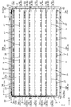
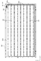
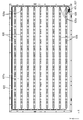
- the top view which shows arrangement structure, such as a LED board in a chassis which comprises a backlight apparatus, each wiring, and a wiring protection member
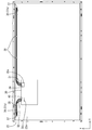
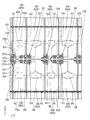
- Bottom view showing an arrangement configuration of LED drive circuit boards and wirings in a chassis constituting the backlight device
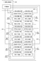
- Enlarged sectional view of the end of the liquid crystal display device Block diagram showing the electrical configuration of the power supply circuit of the LED substrate
- Block diagram showing details of electrical configuration of power supply circuit of LED board
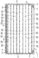
- the top view which shows arrangement structure, such as a LED board in the chassis which concerns on Embodiment 2 of this invention, each wiring, and a wiring protection member.
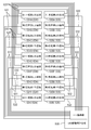
- FIG. 1 Bottom view showing the arrangement configuration of the LED drive circuit board and each wiring in the chassis
- Block diagram showing the electrical configuration of the power supply circuit of the LED substrate
- the top view which shows arrangement structure, such as a LED board in a chassis which concerns on Embodiment 7 of this invention, each wiring, and a wiring protection member.
- FIGS. 1 A first embodiment of the present invention will be described with reference to FIGS.
- the liquid crystal display device 10 is illustrated.
- a part of each drawing shows an X axis, a Y axis, and a Z axis, and each axis direction is drawn to be a direction shown in each drawing.
- the upper side shown in FIG.7 and FIG.8 be a front side, and let the lower side of the figure be a back side.
- a liquid crystal display device 10 is a display device, the front and back both cabinets Ca accommodating so as to sandwich the liquid crystal display device 10, and Cb, since the power supply Power supply circuit board P, a tuner (receiving unit) T capable of receiving a TV image signal, an image conversion circuit board VC for converting the TV image signal output from the tuner T into an image signal for the liquid crystal display device 10 And a stand S.
- the liquid crystal display device 10 a shape towards the horizontal (longitudinal) as a whole (a rectangular shape), and the long-side direction horizontal direction (X-axis direction), a short-side direction perpendicular (Y-axis direction, the vertical direction) and They are housed in a state of almost matching each other.
- the liquid crystal display device 10 includes a liquid crystal panel 11 that is a display panel and a backlight device (illumination device) 12 that is an external light source, which are integrated by a frame-like bezel 13 or the like. Is supposed to be retained.
- the configuration of the liquid crystal panel 11 in the liquid crystal display device 10 will be described.
- the liquid crystal panel 11 has a horizontally long (longitudinal) rectangular shape (rectangular shape) as a whole.
- a pair of transparent (translucent) glass substrates 11a and 11b And a liquid crystal layer 11c containing liquid crystal, which is a substance whose optical characteristics change with application of an electric field.
- the substrates 11a and 11b maintain a gap corresponding to the thickness of the liquid crystal layer. In the state, they are bonded together by a sealing agent (not shown).
- polarizing plates 11d and 11e are attached to the outer surface sides of both the substrates 11a and 11b, respectively. Note that the long side direction of the liquid crystal panel 11 coincides with the X-axis direction, and the short side direction coincides with the Y-axis direction.
- the front side is the CF substrate 11a
- the back side is the array substrate 11b.
- TFTs Thin Film Transistors
- pixel electrodes 15 which are switching elements are matrixed.
- a large number of gate wirings 16 and source wirings 17 are arranged around the TFTs 14 and the pixel electrodes 15 so as to surround the TFTs 14 and the pixel electrodes 15.
- the pixel electrode 15 has a vertically long (longitudinal) rectangular shape (rectangular shape) in which the long side direction coincides with the Y-axis direction and the short side direction coincides with the X-axis direction. It consists of a transparent electrode such as (Zinc Oxide).
- the gate wiring 16 and the source wiring 17 are connected to the gate electrode and the source electrode of the TFT 14, respectively, and the pixel electrode 15 is connected to the drain electrode of the TFT 14. Further, as shown in FIG. 3, an alignment film 18 for aligning liquid crystal molecules is provided on the TFT 14 and the pixel electrode 15 on the liquid crystal layer 11c side.
- a terminal portion led out from the gate wiring 16 and the source wiring 17 is formed at an end portion of the array substrate 11b, and a driver component for driving a liquid crystal (not shown) is connected to the anisotropic conductive film (not shown).
- ACF isotropic Conductive Film
- the driver component for driving the liquid crystal is electrically connected to a display control circuit board (not shown) via various wiring boards.
- This display control circuit board is connected to an image conversion circuit board VC (see FIG. 1) in the television receiver TV, and each wiring 16, 17 via a driver component based on an output signal from the image conversion circuit board VC. It is assumed that a drive signal is supplied to.
- a color filter 19 in which the portions R, G, B, and Y are arranged in a matrix (matrix) is provided.
- the color filter 19 according to the present embodiment includes a yellow colored portion Y in addition to a red colored portion R, a green colored portion G, and a blue colored portion B that are the three primary colors of light.
- the colored portions R, G, B, and Y selectively transmit light of each corresponding color (each wavelength).
- Each colored portion R, G, B, Y has a vertically long (longitudinal) rectangular shape (rectangular shape) in which the long side direction coincides with the Y-axis direction and the short side direction coincides with the X-axis direction, like the pixel electrode 15. I am doing.
- a lattice-shaped light shielding layer (black matrix) BM is provided to prevent color mixing.
- a counter electrode 20 and an alignment film 21 are sequentially stacked on the color filter 19 on the CF substrate 11 a on the liquid crystal layer 11 c side.
- the colored portions R, G, B, and Y constituting the color filter 19 will be described in detail.
- the colored portions R, G, B, and Y are arranged in a matrix with the X-axis direction as the row direction and the Y-axis direction as the column direction.
- Y have the same dimension in the column direction (Y-axis direction), but the dimension in the row direction (X-axis direction) is different for each colored portion R, G, B, Y.
- the colored portions R, G, B, and Y are arranged in the row direction in the order of the red colored portion R, the green colored portion G, the blue colored portion B, and the yellow colored portion Y from the left side shown in FIG.
- the red colored portion R and the blue colored portion B in the row direction are relatively larger than the yellow colored portion Y and the green colored portion G in the row direction. It is said. That is, the colored portions R and B having relatively large dimensions in the row direction and the colored portions G and Y having relatively small dimensions in the row direction are alternately and repeatedly arranged in the row direction. Thereby, the area of the red coloring part R and the blue coloring part B is made larger than the areas of the green coloring part G and the yellow coloring part Y. The areas of the blue colored portion B and the red colored portion R are equal to each other. Similarly, the areas of the green colored portion G and the yellow colored portion Y are equal to each other. 3 and 5 show a case where the areas of the red colored portion R and the blue colored portion B are about 1.6 times the areas of the yellow colored portion Y and the green colored portion G. Show.
- the dimension in the row direction (X-axis direction) of the pixel electrode 15 varies from column to column. . That is, among the pixel electrodes 15, the size and area in the row direction of the pixel electrode 15 that overlaps with the red color portion R and the blue color portion B are the same as those in the row direction of the pixel electrode 15 that overlaps with the yellow color portion Y and the green color portion G. It is relatively larger than the size and area.
- the gate wirings 16 are all arranged at an equal pitch, while the source wirings 17 are arranged at two different pitches depending on the dimensions of the pixel electrodes 15 in the row direction.
- the liquid crystal display device 10 uses the liquid crystal panel 11 including the color filter 19 including the four colored portions R, G, B, and Y, as shown in FIG.
- the television receiver TV is provided with a dedicated image conversion circuit board VC. That is, the image conversion circuit board VC converts the television image signal output from the tuner T into an image signal of each color of blue, green, red, and yellow, and outputs the generated image signal of each color to the display control circuit board. can do. Based on this image signal, the display control circuit board drives the TFTs 14 corresponding to the pixels of each color in the liquid crystal panel 11 via the wirings 16 and 17, and transmits the colored portions R, G, B, and Y of each color. The amount of light can be appropriately controlled.
- the backlight device 12 is arranged so as to cover the chassis 22 having a substantially box shape having an opening on the light emitting surface side (the liquid crystal panel 11 side), and the opening of the chassis 22. And a frame 26 that is disposed along the outer edge of the chassis 22 and holds the outer edge of the group of optical members 23 between the chassis 22 and the chassis 22. Further, in the chassis 22, the LED 24 arranged opposite to the position directly below the optical member 23 (the liquid crystal panel 11), the LED board 25 on which the LED 24 is mounted, and a position corresponding to the LED 24 on the LED board 25. And a diffusing lens 27 attached to the lens.
- the backlight device 12 is a so-called direct type.
- a holding member 28 that can hold the LED substrate 25 between the chassis 22 and a reflection sheet 29 that reflects the light in the chassis 22 toward the optical member 23 are provided. .
- each component of the backlight device 12 will be described in detail.
- the chassis 22 is made of metal, and as shown in FIGS. 6 to 8, a bottom plate 22a having a horizontally long rectangular shape (rectangular shape, rectangular shape) like the liquid crystal panel 11, and each side (a pair of bottom plates 22a) It consists of a side plate 22b that rises from the outer end of the long side and a pair of short sides toward the front side (light emission side) and a receiving plate 22c that projects outward from the rising end of each side plate 22b. It has a shallow box shape (substantially a shallow dish) that opens toward the top.
- the long side direction of the chassis 22 coincides with the X-axis direction (horizontal direction), and the short side direction coincides with the Y-axis direction (vertical direction).
- a frame 26 and an optical member 23 to be described below can be placed on each receiving plate 22c in the chassis 22 from the front side.
- a frame 26 is screwed to each receiving plate 22c.
- An attachment hole for attaching the holding member 28 is provided in the bottom plate 22 a of the chassis 22.
- a plurality of mounting holes are arranged in a distributed manner corresponding to the mounting position of the holding member 28 on the bottom plate 22a.
- the optical member 23 has a horizontally long rectangular shape in a plan view, like the liquid crystal panel 11 and the chassis 22. As shown in FIGS. 7 and 8, the optical member 23 has an outer edge portion placed on the receiving plate 22c so as to cover the opening of the chassis 22 and between the liquid crystal panel 11 and the LED 24 (LED substrate 25). It is arranged in the middle.
- the optical member 23 includes a diffusion plate 23a disposed on the back side (the LED 24 side, opposite to the light emitting side) and an optical sheet 23b disposed on the front side (the liquid crystal panel 11 side, the light emitting side). .
- the diffusing plate 23a has a structure in which a large number of diffusing particles are dispersed in a substrate made of a substantially transparent resin having a predetermined thickness and has a function of diffusing transmitted light.
- the optical sheet 23b has a sheet shape that is thinner than the diffusion plate 23a, and two optical sheets 23b are laminated. Specific types of the optical sheet 23b include, for example, a diffusion sheet, a lens sheet, a reflective polarizing sheet, and the like, which can be appropriately selected and used.
- the frame 26 has a frame shape along the outer peripheral edge portions of the liquid crystal panel 11 and the optical member 23. An outer edge portion of the optical member 23 can be sandwiched between the frame 26 and each receiving plate 22c (FIGS. 7 and 8). Further, the frame 26 can receive the outer edge of the liquid crystal panel 11 from the rear side, is capable sandwich the outer edge of the liquid crystal panel 11 between the bezel 13 that is disposed on the front side (FIGS. 7 and 8 ).
- the LED 24 is a so-called top type in which the LED 24 is mounted on the LED substrate 25 and the surface opposite to the mounting surface with respect to the LED 24 is a light emitting surface.
- the LED 24 includes an LED chip that emits blue light as a light emission source, and includes a green phosphor and a red phosphor as phosphors that emit light when excited by blue light.
- the LED 24 has a configuration in which an LED chip made of, for example, an InGaN-based material is sealed with a resin material on a substrate portion fixed to the LED substrate 25.
- the LED chip mounted on the substrate part has a main emission wavelength in the range of 420 nm to 500 nm, that is, in the blue wavelength region, and can emit blue light (blue monochromatic light) with excellent color purity. Is done.
- a specific main emission wavelength of the LED chip for example, 451 nm is preferable.
- the resin material that seals the LED chip is excited by the blue phosphor emitted from the LED chip and the green phosphor that emits green light by being excited by the blue light emitted from the LED chip. And a red phosphor emitting red light is dispersed and blended at a predetermined ratio.
- the LED 24 is made up of blue light (blue component light) emitted from these LED chips, green light (green component light) emitted from the green phosphor, and red light (red component light) emitted from the red phosphor. Is capable of emitting light of a predetermined color as a whole, for example, white or blueish white. Since yellow light is obtained by synthesizing the green component light from the green phosphor and the red component light from the red phosphor, the LED 24 includes the blue component light and the yellow component from the LED chip. It can be said that it also has the light of.
- the chromaticity of the LED 24 varies depending on, for example, the absolute value or relative value of the content of the green phosphor and the red phosphor, and accordingly the content of the green phosphor and the red phosphor is adjusted as appropriate. Thus, the chromaticity of the LED 24 can be adjusted.
- the green phosphor has a main emission peak in the green wavelength region of 500 nm to 570 nm
- the red phosphor has a main emission peak in the red wavelength region of 600 nm to 780 nm. It is said.
- the green phosphor and the red phosphor provided in the LED 24 will be described in detail.
- ⁇ -SiAlON which is a kind of sialon phosphor
- the sialon-based phosphor is a substance in which a part of silicon atoms of silicon nitride is replaced with aluminum atoms and a part of nitrogen atoms with oxygen atoms, that is, a nitride.
- a sialon-based phosphor that is a nitride is superior in luminous efficiency and durability as compared with other phosphors made of, for example, sulfides or oxides.
- “excellent in durability” specifically means that, even when exposed to high-energy excitation light from an LED chip, the luminance does not easily decrease over time.
- rare earth elements eg, Tb, Yg, Ag, etc.
- ⁇ -SiAlON which is a kind of sialon-based phosphor, has a general formula Si6-zAlzOzN8-z: Eu (z indicates a solid solution amount) or (Si, Al) in which aluminum and oxygen are dissolved in ⁇ -type silicon nitride crystal. ) 6 (O, N) 8: A substance represented by Eu.
- the ⁇ -SiAlON for example, Eu (europium) is used as an activator, and thereby the color purity of green light, which is emitted light, is particularly high. It is extremely useful in adjusting On the other hand, as the red phosphor, it is preferable to use casoon, which is a kind of cascading phosphor.
- Cousin-based phosphors are nitrides containing calcium atoms (Ca), aluminum atoms (Al), silicon atoms (Si), and nitrogen atoms (N). For example, other phosphors made of sulfides, oxides, etc. In comparison, it is excellent in luminous efficiency and durability.
- the cascading phosphor uses rare earth elements (for example, Tb, Yg, Ag, etc.) as an activator.
- Casun which is a kind of cousin phosphor, uses Eu (europium) as an activator and is represented by the composition formula CaAlSiN3: Eu.
- the LED substrate 25 has a base material that is horizontally long when viewed in a plane.
- the long side direction coincides with the X axis direction
- the short side direction coincides with the Y axis direction.
- the chassis 22 is accommodated while extending along the bottom plate 22a.
- the LED 24 is surface-mounted on the plate surface facing the front side (the surface facing the optical member 23 side).
- the mounted LED 24 has a light emitting surface facing the optical member 23 (the liquid crystal panel 11) and an optical axis that coincides with the Z-axis direction, that is, the direction orthogonal to the display surface of the liquid crystal panel 11.
- LEDs 24 are linearly arranged along the long side direction (X-axis direction) on the LED substrate 25 and are connected to the LEDs 24 arranged in parallel.
- a pattern 25c (see FIG. 13) is formed.
- the arrangement pitch of the LEDs 24 is substantially constant, that is, it can be said that the LEDs 24 are arranged at substantially equal intervals in the X-axis direction.
- the LED substrate 25 having the above-described configuration is arranged in parallel in the chassis 22 in a state where the long side direction and the short side direction are aligned with each other in the X-axis direction and the Y-axis direction. ing. That is, the LED substrate 25 and the LED 24 mounted thereon are both set in the X-axis direction (the long side direction of the chassis 22 and the LED substrate 25) in the chassis 22 and in the Y-axis direction (the chassis 22 and the LED substrate 25).
- the short side direction is arranged in a matrix with the column direction (arranged in a matrix, planar arrangement).
- two LED boards 25 are arranged in parallel in a matrix in the chassis 22, two in the X-axis direction (row direction) and nine in the Y-axis direction (column direction). ing.
- the LED substrates 25 are arranged at an equal pitch in the Y-axis direction and are arranged at almost equal intervals.
- a through hole 25b through which the holding member 28 passes is formed at a position corresponding to the mounting position of the holding member 28 in the LED substrate 25 (FIGS. 7 and 8).
- the base material of the LED substrate 25 is made of a metal such as an aluminum material same as that of the chassis 22, and a wiring pattern (not shown) made of a metal film such as a copper foil is formed on the surface thereof via an insulating layer.
- a wiring pattern made of a metal film such as a copper foil is formed on the surface thereof via an insulating layer.
- the outermost surface is formed with a reflective layer (not shown) that exhibits white light with excellent light reflectivity.
- insulating materials such as a ceramic.
- the diffusing lens 27 is made of a synthetic resin material (for example, polycarbonate, acrylic, etc.) that is substantially transparent (having high translucency) and has a refractive index higher than that of air. As shown in FIGS. 6 and 8, the diffusion lens 27 has a predetermined thickness and is formed in a substantially circular shape when seen in a plan view so as to individually cover each LED 24 from the front side with respect to the LED substrate 25. That is, each LED 24 is attached so as to overlap with each other when seen in a plan view.
- the diffusing lens 27 can emit light having strong directivity emitted from the LED 24 while diffusing.
- the diffusing lens 27 is disposed at a position that is substantially concentric with the LED 24 in a plan view. In FIG. 7, since the cross-sectional configuration of the holding member 28 is illustrated, the side surface of the diffusing lens 27 disposed on the back side of the drawing is illustrated.
- the holding member 28 will be described.
- the holding member 28 is made of a synthetic resin such as polycarbonate, and has a white surface with excellent light reflectivity. As shown in FIGS. 6 to 8, the holding member 28 is fixed to the chassis 22 by protruding from the main body 28 a toward the back side, that is, the chassis 22 side, along the main body 28 a along the plate surface of the LED substrate 25. Part 28b.
- the main body 28 a has a substantially circular plate shape when seen in a plan view, and can hold at least the LED substrate 25 with the bottom plate 22 a of the chassis 22.
- Fixing portion 28b is capable locking to the LED substrate 25 and the bottom plate through hole 25b is formed in correspondence to the attachment position of the holding member 28 in 22a and the mounting hole bottom plate 22a while penetrating the chassis 22 .
- a plurality of holding members 28 are appropriately distributed in the plane of the LED substrate 25, and are arranged at positions adjacent to the diffusion lens 27 (LED 24) in the X-axis direction. Yes.
- the holding member 28 sandwiches the LED board 25 between the main body 25a and the bottom plate 22a of the chassis 22 without the bottom 29a of the reflection sheet 29 (first).
- 1 holding member and a member (second holding member) that sandwiches the bottom portion 29a of the reflection sheet 29 together with the LED substrate 25 between the main body portion 25a and the bottom plate 22a of the chassis 22 are included.
- the holding member 28 (second holding member) that holds the bottom 29a of the reflection sheet 29 together with the LED substrate 25 is provided with a support portion 28c that protrudes from the main body portion 28a to the front side, and the support portion 28c. Two types are included.
- the support portion 28c can support the optical member 23 (directly the diffusion plate 23a) from the back side, thereby maintaining a constant positional relationship between the LED 24 and the optical member 23 in the Z-axis direction. And inadvertent deformation of the optical member 23 can be restricted.
- the reflection sheet 29 is made of a synthetic resin, and the surface thereof is white with excellent light reflectivity. As shown in FIGS. 6 to 8, the reflection sheet 29 has a size that is laid over almost the entire inner surface of the chassis 22, so that all the LED boards 25 arranged in parallel in the chassis 22 are arranged. Covering from the front side is possible. The reflection sheet 29 can efficiently raise the light in the chassis 22 toward the optical member 23 side.
- the reflection sheet 29 extends along the bottom plate 22a of the chassis 22 and covers a large portion of the bottom plate 22a.
- the reflection sheet 29 rises from each outer end of the bottom portion 29a to the front side and is inclined with respect to the bottom portion 29a.
- the four rising portions 29b are formed, and the extending portions 29c that extend outward from the outer ends of the respective rising portions 29b and are placed on the receiving plate 22c of the chassis 22 are configured.
- the bottom portion 29 a of the reflection sheet 29 is arranged so as to overlap the front side surface of each LED substrate 25, that is, the mounting surface of the LED 24. Further, the bottom 29a of the reflection sheet 29 is provided with a lens insertion hole through which each diffusion lens 27 is inserted at a position overlapping with each diffusion lens 27 (each LED 24) in plan view.
- the bottom portion 29a is provided with a holding member insertion hole for passing the fixing portion 28b at a position overlapping with each holding member 28 in plan view, and particularly holds the LED substrate 25 without passing through the bottom portion 29a.
- the holding member insertion hole corresponding to the holding member 28 (first holding member) is set to a size that allows the main body portion 28a to pass therethrough.
- the color filter 19 of the liquid crystal panel 11 according to the present embodiment is colored yellow in addition to the colored portions R, G, and B which are the three primary colors of light, as shown in FIGS. Since the portion Y is included, the color gamut of the display image displayed by the transmitted light is expanded, so that a display with excellent color reproducibility can be realized. In addition, since the light transmitted through the yellow colored portion Y has a wavelength close to the peak of visibility, the human eye tends to perceive brightly even with a small amount of energy. Thereby, even if it suppresses the output of LED24 which the backlight apparatus 12 has, sufficient brightness
- the display image of the liquid crystal panel 11 tends to be yellowish as a whole.
- the chromaticity in the LED 24 is adjusted to a blue color that is a complementary color of yellow, thereby correcting the chromaticity in the display image.
- the LED 24 of the backlight device 12 has the main emission wavelength in the blue wavelength region and the highest light emission intensity in the blue wavelength region. ing.
- the area ratio of the blue colored portion B constituting the color filter 19 is set to be relatively larger than that of the green colored portion G and the yellow colored portion Y, whereby the color filter
- the 19 transmitted light can contain more blue light which is a complementary color of yellow.
- the brightness of the red light among the light emitted from the liquid crystal panel 11 is lowered. This is because, in the four primary color type liquid crystal panel 11, compared to the three primary color type, the number of subpixels constituting one pixel increases from three to four, so the area of each subpixel decreases. It is presumed that the brightness of the red light is particularly lowered due to this.
- the area ratio of the red colored portion R constituting the color filter 19 is set to be relatively larger than that of the green colored portion G and the yellow colored portion Y, whereby the color filter
- the transmitted light of 19 can contain a larger amount of red light, so that it is possible to suppress a decrease in lightness of the red light caused by the color filter 19 having four colors.
- the LED board 25 is supplied with electric power from an LED drive circuit board (power supply board) 30 to drive each LED 24 mounted on the LED board 25. It is possible to control.
- the wires 31 to 33 for supplying electric power include LEDs adjacent to each other in the X-axis direction, in addition to the positive electrode side wire 31 and the negative electrode side wire 32 that connect the LED drive circuit board 30 and the LED board 25, respectively.
- a relay wiring 33 that connects the boards 25 and relays power supply between the LED boards 25 is included.
- the LED drive circuit board 30 is connected to a power supply circuit board P (see FIG. 1) that is a power supply source of the liquid crystal display device 10 and is supplied with power.
- the LED drive circuit board 30 will be described. As shown in FIG. 10, the LED drive circuit board 30 is attached to the back side of the bottom plate 22a of the chassis 22, that is, the face opposite to the face on which the LED board 25 is disposed. In other words, the LED drive circuit board 30 sandwiches the bottom plate 22a of the chassis 22 from the front and back with the LED board 25.
- the LED drive circuit board 30 has a positive power supply board connector 30a into which a positive power supply board wiring connector 39 of a positive electrode wiring 31 to be described later is fitted and connected, and a negative power supply board wiring connector 40 of the negative wiring 32. Are connected to the negative side power supply board connector 30b. As shown in FIG.
- the positive power supply board connector 30a has a built-in positive power supply terminal section 30c
- the negative power supply board connector 30b has a built-in negative power supply terminal section 30d.
- the positive-side power terminal portion 30c and the negative-side power terminal portion 30d are provided in the same number as the positive-side wiring 31 and the negative-side wiring 32, which will be described later, and the number of the positive-side power-supply terminal portions 30c and the negative-electrode-side power terminal portions 30d are the same as the number of power supply circuits. (FIG. 12).
- a predetermined voltage is applied to the LED drive circuit board 30 between the positive power terminal part 30c and the negative power terminal part 30d described above, so that a direct current is applied to the LEDs 24 included in each LED board 25.
- An LED driving unit 30e that supplies and drives them is provided.
- the LED drive unit 30e can apply different voltages for each set of positive electrode side power supply terminal units 30c and negative electrode side power supply terminal units 30d (systems of power supply circuits).
- the LED drive circuit board 30 is eccentric to the upper side in the vertical direction in the chassis 22, and to the left side (the negative electrode side LED board 35 side to be described later) shown in FIG. 10 in the horizontal direction. It is arranged at the position.
- the light source board connector 25a is provided. To this light source board connector 25a, wiring connectors 39 to 42 provided on the wirings 31 to 33 side, which will be described in detail later, are fitted and connected. As shown in FIG. 13, the light source substrate connector 25a has both ends of a wiring pattern 25c formed on the LED substrate 25 and an anode side terminal portion 25d connected to one end side of the wiring pattern 25c.
- a cathode side terminal portion 25e connected to the other end side of the wiring pattern 25c is incorporated.
- the wiring pattern 25c extends along the long side direction on the LED substrate 25 and has a folded shape. Specifically, a portion extending from the anode side terminal portion 25d as a starting point crosses the adjacent LEDs 24.
- these LED 24 groups are connected in series and reach the end of the LED board 25 opposite to the light source board connector 25a. By the way, it is set as the form extended linearly toward the cathode side terminal part 25e of the light source board
- each group of LEDs 24 on the two LED substrates 25 forming this set includes The wirings 31 to 33 are connected in series to the LED drive circuit board 30.
- the left side of the figure is the positive side LED board 34 arranged on the positive side in the power feeding circuit
- the right side of the figure is the negative side in the power feeding circuit.
- the negative electrode substrate 35 is disposed on the side.
- the positive-side LED board 34 and the negative-side LED board 35 are arranged in a line along the Y-axis direction, respectively, and nine pieces are arranged in parallel to form nine sets.
- the power supply circuit for the LED board 25 is independent for each set of LED boards 25, and there are nine systems in total.
- the light source board connector 25a included in the positive LED board 34 is a positive light source board connector 34a
- the board connector 25a included in the negative LED board 35 is a negative light source board connector 35a.
- the nine positive-side LED boards 34 arranged in parallel in the column direction on the bottom plate 22a of the chassis 22 are shown in FIG.
- the first negative electrode side LED substrate 35A, the second negative electrode side LED substrate 35B,..., The eighth negative electrode side LED substrate 35H, and the ninth negative electrode side LED substrate 35I will be described in order from the upper side shown in FIG.
- the first positive electrode side LED board 34A and the first negative electrode side LED board 35A adjacent to each other in the X-axis direction constitute the first set, and the second positive electrode side LED board 34B and the second negative electrode side LED board 35B second.
- the eighth positive electrode side LED substrate 34H and the eighth negative electrode side LED substrate 35H are the eighth set, and the ninth positive electrode side LED substrate 34I and the ninth negative electrode side LED substrate 35I are the ninth one.
- Each set is composed.
- the bottom plate 22a of the chassis 22 includes A wiring insertion hole 36 is formed through the positive electrode side wiring 31 and the negative electrode side wiring 32 for connecting them.
- a pair of wiring insertion holes 36 are arranged on the outer edge portion of the bottom plate 22a of the chassis 22, and more specifically, are arranged near both corners on the upper side in the vertical direction of the bottom plate 22a.
- wiring insertion hole 36 inserts only the positive electrode side wiring 31, whereas the other (the right side, FIG.
- the one dedicated to the negative electrode side wiring 32 is arranged on the bottom plate 22a of the chassis 22 at the end on the negative electrode side light source substrate connector 35a side in the negative electrode side LED substrate 35 in the X-axis direction.
- a wiring protection member 37 that surrounds the edge of the wiring insertion hole 36 is attached to the bottom plate 22a.
- the wiring protection member 37 is made of synthetic resin, and covers the hole edge of the wiring insertion hole 36 over the entire circumference and is held attached to the chassis 22 by sandwiching the hole edge from the front and back.
- the wiring protection member 37 has an opening 37a that overlaps the wiring insertion hole 36 in a plan view and is slightly smaller than the wiring insertion hole 36.
- the wirings 31 and 32 are passed through the opening 37a. As a result, the chassis 22 can be moved back and forth.
- the bottom plate 22a of the chassis 22 has a wiring holding member that is positioned on the routing path of the wirings 31 to 33 (outer edge portion of the chassis 22) and holds the wirings 31 to 33 existing there in a bundled state. 38 is provided.
- the wiring holding member 38 is made of a synthetic resin and has a band shape that can be opened and closed.
- a plurality of wiring holding members 38 are arranged at almost equal intervals in the routing paths of the wirings 31 to 33 and are attached to the outer edge of the chassis 22.
- the wiring holding members 38 are disposed on the inner surface (surface on which the LED board 25 is disposed) side and the outer surface (surface on which the LED drive circuit board 30 is disposed) side of the bottom plate 22a of the chassis 22, respectively.
- Each of the wirings 31 to 33 is made of a covered electric wire, and is arranged so as to be positioned substantially at the outer edge portion of the chassis 22. Specifically, as shown in FIGS. 9 and 11, each of the wirings 31 to 33 is routed in the chassis 22 by using a gap held between the side plate 22b and the LED substrate 25, and The reflective sheet 29 is covered from the front side over the entire area by the respective rising portions 29b having an inclined shape.
- Wiring connectors 39 to 42 are provided at both ends of the wirings 31 to 33, and the power supply board connectors 30a and 30b of the LED drive circuit board 30 corresponding to the wiring connectors 39 to 42 or the LED boards.
- the light source board connectors 34a and 35a of the 34 and 35 can be fitted and connected.
- the wirings 31 to 33 are LED substrates that form a pair with a positive electrode wiring 31 connected to the positive electrode side of the LED drive circuit board 30 and a negative electrode wiring 32 connected to the negative electrode side of the LED drive circuit board 30. And a relay wiring 33 for relay-connecting 25.
- the wirings 31 to 33 and the wiring connectors 39 to 42 will be described in detail individually.
- each wiring connector 39 to 42 will be described.
- a positive power supply board wiring connector 39 provided at the end of the positive wiring 31 is fitted and connected to the positive power supply board connector 30 a in the LED drive circuit board 30.
- the positive-side power supply substrate wiring connector 39 has a built-in positive-side wiring terminal portion 39a connected to one end of the positive-side wiring 31, and the positive-side wiring terminal portion 39a is connected to the positive-side wiring terminal portion 39a.
- the positive power supply terminal portion 30c in the side power supply board connector 30a can be brought into conductive contact.
- the negative electrode side power supply substrate wiring connector 40 provided at the terminal of the negative electrode side wiring 32 is fitted and connected to the negative electrode side power supply substrate connector 30b in the LED drive circuit board 30.
- the negative electrode side power supply substrate wiring connector 40 includes a negative electrode side wiring terminal portion 40a connected to one end side of the negative electrode side wiring 32, and the negative electrode side wiring terminal portion 40a is included in the negative electrode side power supply substrate connector 30b. Conductive contact is possible with the negative power supply terminal portion 30d.
- a positive-side light source board wiring connector 41 provided at the terminals of the positive-side wiring 31 and the relay wiring 33 is fitted and connected to the positive-side light source board connector 34a of the positive-side LED board 34.
- the positive-side light source board wiring connector 41 includes a positive-side wiring terminal portion 41 a connected to the other end of the positive-side wiring 31 and a negative-side wiring terminal portion 41 b connected to one end of the relay wiring 33.
- the positive electrode side wiring terminal portion 41a is connected to the anode side terminal portion 25d in the positive electrode side light source substrate connector 34a
- the negative electrode side wiring terminal portion 41b is connected to the cathode side terminal portion 25e in the positive electrode side light source substrate connector 34a.
- the negative electrode side light source substrate wiring connector 42 provided at the terminal of the negative electrode side wiring 32 and the relay wiring 33 is fitted and connected to the negative electrode side light source substrate connector 35a in the negative electrode side LED substrate 35.
- the negative-side light source board wiring connector 42 includes a positive-side wiring terminal portion 42 a connected to the other end side of the relay wiring 33 and a negative-side wiring terminal portion 42 b connected to the other end side of the negative-side wiring 32.
- the positive electrode side wiring terminal portion 42a is connected to the anode side terminal portion 25d in the negative electrode side light source substrate connector 35a
- the negative electrode side wiring terminal portion 42b is connected to the cathode side terminal portion 25e in the negative electrode side light source substrate connector 35a.
- Each can be in conductive contact.
- the wirings 31 to 33 will be described in more detail.
- one end side of the positive electrode side wiring 31 is connected to the positive electrode side wiring terminal portion 39a accommodated in the positive electrode side power supply substrate wiring connector 39, while the other end side is for the positive electrode side light source substrate.
- the positive electrode side wiring terminal portion 41 a accommodated in the wiring connector 41 is connected.
- the positive-side wiring 31 has one end drawn out to the outside of the back side of the bottom plate 22a through a wiring insertion hole 36 that penetrates the bottom plate 22a of the chassis 22, and the positive-side power supply board provided at one end there
- the wiring connector 39 is fitted and connected to the positive power supply board connector 30a on the LED drive circuit board 30 side. As shown in FIG.
- the positive electrode side wiring 31 is arranged in a substantially L shape in plan view along the outer edge of the bottom plate 22 a in the chassis 22 and is provided on the other end side.
- the wiring connector 41 is fitted and connected to the corresponding positive-side light source board connector 34a.
- the positive electrode-side wiring 31 is bent from the dedicated wiring insertion hole 36 to the left side shown in FIG. 9 along the X-axis direction and then bent substantially at a right angle along the Y-axis direction (vertical direction). While extending downward, it is routed along a space held between the side plate 22b and the end of the positive LED board 34 on the positive light source board connector 34a side.
- the positive-side wirings 31 provided in the same number as the sets of LED boards 25 have different wiring lengths according to the positional relationship in the Y-axis direction between the positive-side LED boards 34A to 34I to be connected and the wiring insertion holes 36.
- the one connected to the first positive electrode side LED board 34A located closest to the upper side in the vertical direction (closest to the wiring insertion hole 36) is the shortest, whereas the most vertical The longest is the one connected to the ninth positive-side LED board 34I located at the lower side of the direction (the farthest from the wiring insertion hole 36).
- one end side of the negative electrode side wiring 32 is connected to the negative electrode side wiring terminal portion 40a accommodated in the negative electrode side power supply substrate wiring connector 40, while the other end side is for the negative electrode side light source substrate. It is connected to the negative electrode side wiring terminal portion 42 b accommodated in the wiring connector 42.
- the negative electrode side wiring 32 has one end drawn out to the outside of the back side of the bottom plate 22 a through a wiring insertion hole 36 penetrating the bottom plate 22 a of the chassis 22, and the negative side power The board wiring connector 40 is fitted and connected to the negative power supply board connector 30b on the LED drive circuit board 30 side. As shown in FIG.
- the negative electrode side wiring 32 is arranged in a substantially L shape in plan view along the outer edge of the bottom plate 22 a in the chassis 22 and is provided on the other end side.
- the wiring connector 42 is fitted and connected to the corresponding negative-side light source board connector 35a.
- the negative electrode side wiring 32 is bent from the dedicated wiring insertion hole 36 to the right side shown in FIG. 9 along the X-axis direction, and then bent substantially at a right angle along the Y-axis direction (vertical direction). While extending downward, it is routed along the space held between the side plate 22b and the end of the negative LED substrate 35 on the negative light source substrate connector 35a side.
- the negative electrode side wires 32 provided in the same number as the set of LED substrates 25 have different wire lengths depending on the positional relationship in the Y axis direction between the negative electrode side LED substrates 35A to 35I to be connected and the wire insertion holes 36.
- the one connected to the first negative LED substrate 35A is the shortest, while the one connected to the ninth negative LED substrate 35I is the longest.
- the negative electrode side wiring 32 is substantially symmetrical with the positive electrode side wiring 31 at least in the chassis 22.
- the relay wiring 33 has one end connected to the negative electrode terminal terminal 41b accommodated in the positive light source substrate wiring connector 41, while the other end is connected to the negative light source substrate wiring.
- the positive electrode side wiring terminal portion 42 a accommodated in the connector 42 is connected.
- the relay wiring 33 is accommodated in the chassis 22 over the entire length and the entire area, and the outer edge of the chassis 22 on the side where the wiring insertion hole 36 is provided (see FIG. 9).
- the positive electrode described above along a substantially gate-shaped region extending between a pair of outer edge portions (outer edge portions on the left and right sides shown in FIG. 9) adjacent to both sides thereof.
- the side wiring 31 and the negative side wiring 32 are bundled together by a wiring holding member 38.
- the ends of the wirings 31 to 33 branch out toward the corresponding positive LED board 34 or negative LED board 35 side, and are connected to the terminals.
- the provided positive side light source board wiring connector 41 or negative side light source board wiring connector 42 is fitted and connected to the corresponding positive side light source board connector 34a or negative side light source board connector 35a.
- the relay wiring 33 provided in the same number as the set of LED boards 25 is positioned in the Y-axis direction (vertical direction) in the chassis 22 in the positive-side LED boards 34A to 34I and the negative-side LED boards 35A to 35I to be connected.
- the first and second negative LED substrates 34A and 35A are located on the uppermost side in the vertical direction (closest to the wiring insertion hole 36) and specifically the first negative LED side substrate 35A. Is connected to the ninth positive electrode side LED board 34I and the ninth negative electrode side LED board 35I that are located on the lowermost side in the vertical direction (the furthest away from the wiring insertion hole 36). The one to do is the longest. Note that the length of the pair of portions extending along the Y-axis direction is substantially equal to each other in the relay wiring 33 and has a substantially symmetrical shape as a whole.
- the above-described three types of wirings 31 to 33 are color-coded so that the surface colors are different from each other, and specifically, the surfaces of the insulating coating covering the core wires have different colors.
- the positive electrode side wiring 31, the negative electrode side wiring 32, and the relay wiring 33 are color-coded into two colors according to the power supply circuit system, respectively, for a total of six colors.
- the positive electrode side wiring 31, the negative electrode side wiring 32, and the relay wiring 33, among the LED substrates 25, form positive-numbered LED substrates 34 ⁇ / b> A, 34 ⁇ / b> C, 34E, 34G, 34I and the negative side LED boards 35A, 35C, 35E, 35G, 35I connected to the respective light source board wiring connectors 41, 42 fitted to the respective light source board connectors 34a, 35a;
- Different colors are connected to those connected to 41 and 42. Specifically, as shown in FIG.
- the surfaces of the positive electrode side wirings 31A and 31B are color-coded into green and blue, and the negative electrode side wirings 32A and 32B are color-coded into black and gray, and the relay wiring 33A, 33B is color-coded into red and white, and the former (green positive-side wiring 31A, black negative-side wiring 32A, red relay wiring 33A) is connected to the power supply circuit related to the odd-numbered group by the latter ( The blue positive-side wiring 31B, the gray negative-side wiring 32B, and the white relay wiring 33B) respectively correspond to the power feeding circuits according to the even-numbered groups.
- the LED boards 25 on which the LEDs 24 are mounted are accommodated in the chassis 22, and the holding member 28 (first holding member) while being aligned at a predetermined position.
- the wiring protection member 37 is attached in advance to the hole edge of the wiring insertion hole 36 of the chassis 22.
- the wirings 31 to 33 are formed into wire harnesses in advance, and the wiring connectors 39 to 42 are respectively provided at the terminals.
- the bundle of the wires 31 to 33 is routed along the outer edge portion of the chassis 22 in the chassis 22, the bundle of the wires 31 to 33 is held by the wire holding member 38 arranged on the routing path.
- the light source board wiring connectors 41 and 42 are pulled out from the bundle to the corresponding LED boards 34 and 35 (see FIG. 9).
- the wiring work of the wirings 31 to 33 and the drawing work of the light source board wiring connectors 41 and 42 can be smoothly performed.
- the pulled-out positive-side light source board wiring connector 41 is fitted and connected to the positive-side light source board connector 34a in the corresponding positive-side LED board 34, and the negative-side light source board wiring connector 42 is connected to the corresponding negative electrode.
- the negative LED side light source board connector 35a in the side LED board 35 is fitted and connected (see FIG. 9).
- the positive-side LED board 34 and the negative-side LED board 35 constitute nine groups for each of the power feeding circuits independent of each other, and each light source board connector 34a, 35a is for each light source board.
- the wiring connectors 41 and 42 need to be accurately associated and fitted.
- the corresponding connectors 34a, 35a, 41, and 42 can be accurately fitted to each other without making a wrong mating partner (See FIG. 12). Note that the above-described work procedure can be changed as appropriate. For example, after the connectors 34a, 35a, 41, and 42 are fitted, the wires 31 to 33 are held by the wire holding member 38. It doesn't matter.
- each diffusing lens 27 LED 24
- each lens insertion hole in the bottom 29a of the reflection sheet 29 while being aligned
- each extending portion 29c is placed on each receiving plate 22c.
- a holding member (second holding member) 28 the bottom portion 22 a is fastened together with the LED substrate 25 to the bottom plate 22 a of the chassis 22.
- each optical member 23 is mounted on the extension part 29c so that the opening part of the chassis 22 may be covered.
- the LED drive circuit board 30 is attached to a predetermined position on the back side of the bottom plate 22a and the positive side wiring 31 is connected to the positive side power board connector 30a.
- the positive side power supply board wiring connector 39 arranged at the terminal of the negative electrode side power supply board connector 30b is fitted and connected to the negative electrode side power supply board wiring connector 40 arranged at the terminal of the negative electrode side wiring 32.
- the backlight device 12 is manufactured.
- the liquid crystal display device 10 is manufactured by sequentially assembling the frame 26, the liquid crystal panel 11, and the bezel 13 to the backlight device 12.
- the drive power output from the LED drive circuit board 30 is supplied to the positive-side LED board 34 via the positive-side wiring 31, and then forms the same set via the relay wiring 33. It is supplied to the LED substrate 35. That is, since the plurality of LEDs 24 mounted on the positive-side LED board 34 and the negative-side LED board 35 forming the same set are connected to each other in series, with substantially the same luminance according to the value of the supplied voltage. Illuminated. And in the backlight apparatus 12 in this embodiment, as shown in FIG. 12, since the electric power feeding circuit is independent for each set of LED boards 25, the magnitude of the voltage supplied to each set is freely set. It is possible to set.
- the brightness of the LED 24 can be made different for each set by changing the magnitude of the voltage supplied to all the sets, and the magnitude of the voltage supplied to each set and the LED 24 belonging to the set can be made different.
- the brightness can be varied, and the voltage magnitude and the brightness of the LED 24 can be the same in all sets.
- the power supply circuit according to the present embodiment has a configuration in which the positive-side LED board 34 and the negative-side LED board 35 are connected by the relay wiring 33, and thus a relay connector as used in the related art is required. A connection structure that does not occur is realized. Since this relay connector is a structure that protrudes from the LED substrate 25, it is necessary to form an opening in the bottom 29a of the reflection sheet 29 so that the relay connector can be prevented from being uneven. . However, when the relay connector is exposed in the chassis 22 through the hole of the reflection sheet 29, the light reflectance on the surface thereof is lower than that of the reflection sheet 29, so that it may be visually recognized as a dark part.
- the connection structure that does not require the relay connector since the connection structure that does not require the relay connector is employed, the occurrence of dark portions due to the relay connector as described above is prevented, and thus uneven brightness is unlikely to occur.
- the two LED boards 34 and 35 forming the same set are connected by the relay wiring 33, and the LED boards 34 and 35 are connected to the positive-side wiring 31 and the negative-side wiring one by one. 32, the LED drive circuit board 30 is connected to the LED drive circuit board 30.
- the positive electrode side wiring and the negative electrode side wiring are prepared for each LED board, and each LED board is individually connected to the LED drive circuit board 30.
- the wiring length can be shortened. Since the positive electrode side wiring 31 and the negative electrode side wiring 32 are routed into and out of the chassis 22 through the wiring insertion holes 36 in the bottom plate 22a of the chassis 22, workability related to routing is reduced by reducing the number of the wirings. Can be remarkably improved, and the manufacturing cost can be reduced.
- the backlight device (illumination device) 12 of this embodiment includes the LED drive circuit board (power supply board) that can supply power, and the positive electrode-side wiring 31 that has one end connected to the LED drive circuit board 30.
- the LED (light source) 24 is mounted and the other end side of the positive electrode side wiring 31 is connected to the positive electrode side LED substrate (positive electrode side light source substrate) 34, and one end side is connected to the LED drive circuit substrate 30.
- the side wiring 32 and the LED 24 are mounted and the other end side of the negative side wiring 32 is connected to the negative side LED substrate (negative side light source substrate) 35, one end side to the positive side LED substrate 34, and the other end side to By being connected to the negative-side LED board 35, the relay wiring 33 is provided to relay the supply of power from the positive-side LED board 34 side to the negative-side LED board 35 side.
- each of the LED substrates can be obtained by electrically connecting the positive side LED board 34 and the negative side LED board 35 to the LED drive circuit board 30 by the positive side wiring 31, the relay wiring 33, and the negative side wiring 32. Electric power can be supplied to the LEDs 24 mounted on 34 and 35.
- a relay connector is temporarily mounted on the positive-side LED board and the negative-side LED board, and the relay is performed. A connection structure that does not require a relay connector as in the case where the connectors are connected to each other can be realized.
- this type of relay connector can be a dark part in the backlight device 12, according to the present embodiment, it is possible to make the dark part difficult to occur.
- the positive LED board 34 and the negative LED board 35 are connected by the relay wiring 33, for example, when each LED board is individually connected to the LED drive circuit board 30
- the number of wirings connecting the LED drive circuit board 30 and the LED boards 34 and 35 can be reduced compared to the case where the positive electrode side wiring 31 and the negative electrode side wiring 32 are required for each LED board 34 and 35.
- the overall wiring length can be shortened. Thereby, the workability related to assembly can be improved, and the cost related to manufacturing can be reduced. According to the present embodiment, luminance unevenness hardly occurs, and the workability related to assembly can be improved and the manufacturing cost can be reduced.
- a chassis 22 in which the positive LED substrate 34 and the negative LED substrate 35 are accommodated is provided, and the positive electrode wiring 31, the negative electrode wiring 32, and the relay wiring 33 are arranged on the outer edge portion of the chassis 22.
- the positive electrode side wiring 31, the negative electrode side wiring 32 and the relay wiring 33 connected to the positive electrode side LED substrate 34 and the negative electrode side LED substrate 35 accommodated in the chassis 22 are arranged on the outer edge portion of the chassis 22.
- These wirings 31 to 33 are difficult to be visually recognized as dark portions.
- the chassis 22 has a bottom plate 22a for receiving the positive LED board 34 and the negative LED board 35.
- the bottom plate 22a has a surface on which the positive LED board 34 and the negative LED board 35 are disposed.
- the LED driving circuit board 30 is attached to the opposite surface, and a wiring insertion hole 36 for passing the positive side wiring 31 and the negative side wiring 32 is formed therethrough.
- each of the LED boards 34 and 35 and the LED drive circuit board 30 arranged on the opposite sides of the bottom plate 22a is connected to the positive electrode side wiring 31 through the wiring insertion hole 36 penetrating the bottom plate 22a.
- the negative-side wiring 32 are connected to each other.
- a wiring protection member 37 is attached to the bottom plate 22a so as to surround the hole edge of the wiring insertion hole 36. In this way, it is possible to avoid the positive electrode side wiring 31 and the negative electrode side wiring 32 from directly interfering with the hole edge of the wiring insertion hole 36 in the bottom plate 22a by the wiring protection member 37. It is possible to prevent disconnection, and the connection reliability is excellent.
- the wiring insertion hole 36 is composed of at least two of the one through which the positive electrode side wiring 31 is passed and the one through which the negative electrode side wiring 32 is passed.
- the dedicated wiring insertion hole 36 through which the positive electrode side wiring 31 passes and the dedicated wiring insertion hole 36 through which the negative electrode side wiring 32 passes are included. It becomes easy to distinguish from the side wiring 32 and contributes to the improvement of workability.
- the degree of freedom of the arrangement of the respective wiring insertion holes 36 in the bottom plate 22a is high, the degree of freedom of the routing path of the positive side wiring 31 and the negative side wiring 32 is also increased. It can be made shorter.
- the chassis 22 in which the positive LED substrate 34 and the negative LED substrate 35 are accommodated is provided, and the chassis 22 covers the positive LED substrate 34 and the negative LED substrate 35 while passing the LEDs 24.
- a reflection sheet (reflecting member) 29 that reflects light from the LED 24 toward the light emitting side is provided, and the reflection sheet 29 is arranged so as to cover the positive electrode side wiring 31, the negative electrode side wiring 32, and the relay wiring 33. Yes.
- the LED boards 34 and 35 and the wirings 31 to 33 are covered with the reflection sheet 29, so that the LED boards 34 and 35 and the wirings 31 to 33 are difficult to be visually recognized as dark portions, thereby causing uneven brightness. It is suitable for prevention.
- the positive electrode side wiring 31, the negative electrode side wiring 32, and the relay wiring 33 each have a different surface color. In this way, when connecting the wirings 31 to 33, the types of the wirings 31 to 33 can be easily distinguished, so that the workability related to the connection can be further improved.
- the positive side LED substrate 34 and the negative side LED substrate 35 are arranged adjacent to each other to form a set, and in addition to the plurality of sets arranged in parallel in a row, the positive side wiring 31
- the negative electrode side wiring 32 and the relay wiring 33 are provided in the same number as the number of sets of the positive electrode side LED substrate 34 and the negative electrode side LED substrate 35.
- the positive electrode side wiring 31, the negative electrode side wiring 32, and the relay wiring 33 are provided on the positive electrode side.
- the set of LED board 34 and negative side LED board 35 the one that is connected to the odd-numbered set in the parallel direction and the one that is connected to the even-numbered set have different colors on the surface It is said.
- each wiring 31 corresponding to each set of the positive-side LED board 34 and the negative-side LED board 35 is enlarged.
- a plurality of LEDs 24 are mounted on the positive LED substrate 34 and the negative LED substrate 35, and a wiring pattern 25c for connecting the plurality of LEDs 24 in series is formed.
- the wiring pattern 25c has a positive electrode on one end side. The other end side is connected to the side wiring 31 or the relay wiring 33 and the other side is connected to the relay wiring 33 or the negative side wiring 32, respectively.
- one end side of the wiring pattern 25c is connected to the positive-side wiring 31 and the other end side is connected to the relay wiring 33, so that power is supplied to the plurality of mounted LEDs 24. Is done.
- one end side of the wiring pattern 25 c is connected to the relay wiring 33 and the other end side is connected to the negative-side wiring 32, whereby electric power is supplied to the plurality of mounted LEDs 24.
- This is suitable when a large number of LEDs 24 are required, and is particularly useful when the backlight device 12 is enlarged.
- wiring connectors 39 to 42 are provided at the terminals of the positive electrode side wiring 31, the negative electrode side wiring 32, and the relay wiring 33, respectively, whereas the positive electrode side LED substrate 34, the negative electrode side LED substrate 35, and the LED driving circuit are provided.
- the board 30 is provided with board connectors 30a, 30b, 34a, and 35a (25a) to which the corresponding wiring connectors 39 to 42 are fitted and connected. In this way, since the connection structure between each of the wirings 31 to 33 and each of the substrates 30, 34, and 35 (25) is made into a connector, it is related to assembly and the like as compared with the case where the connection is made by soldering. Workability can be further improved.
- a wiring insertion hole 136 through which both the positive electrode side wiring 131 and the negative electrode side wiring 132 are inserted is formed through the bottom plate 122a of the chassis 122 according to the present embodiment. Only one wiring insertion hole 136 is formed at the outer edge portion of the bottom plate 122a, which is a so-called common type that allows the positive electrode side wiring 131 and the negative electrode side wiring 132 to pass together.
- the wiring insertion hole 136 is arranged on the right side of the bottom plate 122a shown in FIG. 14, that is, the end on the negative light source board connector 135a side.
- the LED drive circuit board 130 is disposed at a position offset toward the wiring insertion hole 136 in the bottom plate 122 a. Accordingly, the positive electrode side wiring 131 and the negative electrode side wiring 132 both have a very short wiring length from the wiring insertion hole 136 to the power supply board connectors 130a and 130b of the LED drive circuit board 130 outside the back side of the chassis 122.
- the positive-side wiring 131 has a bottom plate 122a extending in the long side direction (X) until reaching the positive-side light source board connector 134a of the positive-side LED board 134 from the wiring insertion hole 136. It is assumed that it traverses almost the entire length along the axial direction.
- Embodiment 3 of the present invention will be described with reference to FIG.
- the wiring routes of the wirings 231 to 233 are changed.
- action, and effect as above-mentioned Embodiment 1 is abbreviate
- the wirings 231 to 233 according to the present embodiment are arranged in the chassis 222 without crossing the outer edge on the upper side in the vertical direction, as shown in FIG. It is routed by a route that crosses. Specifically, the positive electrode side wiring 231 and the negative electrode side wiring 232 are drawn outward along the X-axis direction from the wiring insertion hole 36 in the chassis 222 and then bent substantially at a right angle to extend downward in the vertical direction. By doing so, it is wired so as to form a substantially L shape as a whole.
- the relay wiring 233 is routed over three sides of the outer peripheral edge portion of the chassis 222, that is, a lower outer edge portion in the vertical direction and a pair of outer edge portions that are adjacent to both sides and extend along the vertical direction. It is routed along a substantially gate-shaped region excluding the outer edge on the side where the pair of wiring insertion holes 36 are provided, that is, the outer edge on the upper side in the vertical direction.
- the wirings 231 to 233 do not cross the upper outer edge of the chassis 222 in the vertical direction, so that the wirings 231 to 233 are less likely to sag during use.
- the wirings 231 to 233 are bundled together by a wiring holding member 238 arranged on the wiring path.
- the bottom plate 322a of the chassis 322 is formed with a through hole 336 through which the positive electrode side wire 331 and the negative electrode side wire 332 are inserted.
- the configuration is generally the same. Only one wiring insertion hole 336 is formed at the outer edge of the bottom plate 322a, and is a so-called shared type that is large enough to allow the positive-side wiring 331 and the negative-side wiring 332 to pass together.
- the wiring insertion hole 336 is disposed on the right side of the bottom plate 322a shown in FIG. 17, that is, the end on the negative side light source board connector 335a side (LED drive circuit board side (see FIG. 15)).
- Embodiment 5 A fifth embodiment of the present invention will be described with reference to FIG. In this Embodiment 5, what changed the number of LED boards 425 included in one electric power feeding circuit is shown. In addition, the overlapping description about the same structure, an effect
- the power feeding circuits are three independent from each other, and a single power feeding circuit includes six LED substrates 425. Therefore, the LED substrate 425 included in the power supply circuit includes one connected to the positive electrode side wiring 431 and the relay wiring 433 (positive electrode side LED substrate 434), and one connected to the negative electrode side wiring 432 and the relay wiring 433 (negative electrode). Side LED board 435) and those connected only to the relay wiring 433 (intermediate LED board 43) are included. Specifically, among the six LED boards 425 included in one power supply circuit, the positive-side wiring 431 is not connected to the pair of LED boards 425 closest to the LED drive circuit board 430 on the wiring path of the wirings 431 to 433.
- relay wiring 433 or the negative electrode side wiring 432 and the relay wiring 433 are connected, whereas only the relay wiring 433 is connected to the four LED boards 425 positioned between the pair of LED boards 425.
- the four LED boards 425 connected only to the relay wiring 433 are intermediate LED boards 43 existing between the positive LED board 434 and the negative LED board 435, and the relay wiring 433 connecting them is
- the number of intermediate LED boards 43 includes the divided relay wiring 44 divided into a number obtained by adding 1 (5 in the present embodiment).
- the pair of LED substrates 425G of the eye constitutes a positive LED substrate 434 and a negative LED substrate 435, respectively.
- the pair of LED boards 425B in the second row counted from the upper side in the vertical direction
- the pair of LED boards 425C in the third row the pair of LED boards 425E in the fifth row, and the pair in the sixth row.
- the LED board 425F, the pair of LED boards 425H in the eighth row, and the pair of LED boards 425I in the ninth row constitute the intermediate LED board 43, respectively.
- the pair of intermediate LED boards 43 (425B) in the second row, the pair of intermediate LED boards 43 (425E) in the fifth row, and the pair of intermediate LED boards 43 (425H) in the eighth row are respectively positive side LEDs.
- the pair of intermediate LED boards 43 (425I) are arranged such that another intermediate LED board 43 is interposed between the positive LED board 434 and the negative LED board 435, respectively.
- the pair of intermediate LED boards 43 (425B) in the second row are respectively connected to the positive LED board 434 (425A) and the negative LED board 435 (425A) in the first row by a pair of divided relay wirings 44, respectively.
- the pair of intermediate LED boards 43 (425C) in the third row are connected to the pair of intermediate LED boards 43 (425B) in the second row by a pair of divided relay wirings 44, respectively.
- a pair of intermediate LED boards 43 (425C) are connected by a single split relay wiring 44.
- those connecting the intermediate LED substrates 43 in different rows connect the intermediate LED substrates 43 in the same row, although the wiring length is about the arrangement pitch between the intermediate LED substrates 43. Since the wiring length of the thing more than the magnitude
- the intermediate LED boards 43 (425E, 425F, 425H, 425I) in the 5th, 6th, 8th, and 9th rows are also connected in the same manner as the second and third rows described above. Specifically, the fifth and sixth rows are connected to the fourth row, and the eighth and ninth rows are connected to the seventh row by divided relay wirings 44, respectively. Yes. Further, a pair of split relay wiring connectors (not shown) that are fitted and connected to the corresponding LED board connectors 25a (see FIG. 9) are provided at both terminals of each split relay wiring 44.
- the number of the positive electrode wires 431 and the negative electrode wires 432 is increased by three. Can be reduced. Thereby, the workability when routing the positive electrode side wiring 431 and the negative electrode side wiring 432 can be further improved, and the manufacturing cost can be further reduced. Moreover, if the number of the positive electrode side wiring 431 and the negative electrode side wiring 432 is reduced, the number of power supply terminal portions (FIG. 13) in the LED drive circuit board 430 can also be reduced. It is possible to make it easier.
- the divided relay wiring 44 that connects the intermediate LED boards 43 in different rows may have a wiring length of about the arrangement pitch between the intermediate LED boards 43, the entire wiring length of the relay wiring 433 is shortened. This is superior in terms of workability at the time of routing and manufacturing costs.
- the intermediate light source substrate (intermediate LED substrate) 43 on which the LEDs 24 are mounted is provided, whereas the relay wiring 433 is composed of a plurality of divided relay wirings 44.
- one end side of each of the plurality of divided relay wirings 44 is connected to the positive LED board 434 and the other end side thereof is connected to the intermediate LED board 43 so that power is supplied from the positive LED board 434 side to the intermediate LED board 43 side.
- relaying power supply from the intermediate LED board 43 side to the negative LED board 435 side by connecting one end side to the intermediate LED board 43 and the other end side to the negative LED board 435, respectively. And are included.
- the intermediate LED board 43 is connected to the positive-side LED board 34 and the negative-side LED board 35.
- the positive-side wiring and the negative-side wiring are different from those connected to the positive-side LED board 34 and the negative-side LED board 35.
- the number of wirings connecting the LED driving circuit board 430 and the LED boards 434 and 435 can be further reduced.
- a plurality of intermediate LED boards 43 are provided, whereas the divided relay wiring 44 has an intermediate LED board 43 different from the intermediate LED board 43 whose one end is connected to the intermediate LED board 43 and the other end is connected to one end. Are included. In this way, power can be supplied to the plurality of intermediate LED boards 43, so that the number of wires connecting the LED drive circuit board 430 and the LED boards 434 and 435 can be further reduced.
- Embodiment 6 A sixth embodiment of the present invention will be described with reference to FIGS. In this Embodiment 6, what changed arrangement
- the pair of wiring insertion holes 536 are respectively disposed in the vicinity of both corner positions in the lower outer edge portion in the vertical direction of the outer peripheral edge portion of the bottom plate 522 a of the chassis 522.
- the LED drive circuit board 530 is arranged at a position offset to the lower side in the vertical direction on the bottom plate 522a of the chassis 522 as shown in FIG.
- the positive side wiring 531 passed through the left side wiring insertion hole 536 shown in FIG. 19 is arranged in an approximately L shape within the chassis 522, and specifically, the wiring insertion hole. 19 is directed to the left side shown in FIG.
- the negative electrode side wiring 532 passed through the right side wiring insertion hole 536 shown in FIG. 19 is arranged in a substantially L shape in the chassis 522, and specifically, from the wiring insertion hole 536 along the X-axis direction. 19 and then bent at a substantially right angle and extended upward along the Y-axis direction (vertical direction), and on the side plate 522b and the negative-side LED board 535 on the negative-side light source board connector 535a side.
- the positive-side wiring 531 and the negative-side wiring 532 are connected in the Y-axis direction between the positive-side LED boards 534A to 534I and the negative-side LED boards 535A to 535I to be connected and the wiring insertion hole 536.
- the wiring lengths are different depending on the positional relationship, and specifically, connected to the ninth positive-side LED board 534I located on the lowermost side in the vertical direction (closest to the wiring insertion hole 536) Is the shortest, the longest is the one connected to the first positive electrode side LED board 534A located on the uppermost side in the vertical direction (the farthest from the wiring insertion hole 536).
- the wiring path of the positive electrode side wiring 531 and the negative electrode side wiring 532 according to the present embodiment is vertically different from the positive electrode side wiring 31 and the negative electrode side wiring 32 (see FIG. 9) according to the first embodiment. Is reversed.
- the relay wiring 533 includes an outer edge of the chassis 522 on the side where the wiring insertion hole 536 is provided (an outer edge on the lower side in the vertical direction shown in FIG. 19),
- the wiring holding member is arranged along a substantially gate-shaped region extending over a pair of outer edge portions (the outer edge portions on the left and right sides shown in FIG. 19) adjacent to both sides, and together with the positive electrode side wiring 531 and the negative electrode side wiring 532 described above. 538 and bundled together.
- Each relay wiring 533 has different wiring lengths depending on the positions in the Y-axis direction (vertical direction) in the chassis 522 of the positive-side LED boards 534A to 534I and the negative-side LED boards 535A to 535I to be connected.
- the one that connects the first positive electrode side LED board 534A and the first negative electrode side LED board 535A that is located on the uppermost side in the vertical direction (the furthest from the wiring insertion hole 536) is the shortest. that whereas, those that connect the most vertical positioned on the lower side (closest to the wiring insertion hole 536) and the ninth positive side LED substrate 534I ninth negative side LED board 535I is the longest.
- the routing route of the relay wiring 533 according to the present embodiment is substantially the same as the relay wiring 33 (see FIG. 9) according to the first embodiment.
- the wiring insertion hole 636 is changed from the above-described sixth embodiment to be similar to the second embodiment.
- movement, and effect as above-mentioned Embodiment 2, 6 is abbreviate
- a wiring insertion hole 636 through which both the positive electrode side wiring 631 and the negative electrode side wiring 632 are inserted is formed in the lower outer edge portion of the bottom plate 622a of the chassis 622 according to the present embodiment in the vertical direction. Yes. Only one wiring insertion hole 636 is formed at the outer edge portion of the bottom plate 622a, and is a so-called shared type that is large enough to allow the positive-side wiring 631 and the negative-side wiring 632 to pass together.
- the wiring insertion hole 636 is disposed on the right side of the bottom plate 622a shown in FIG. 22, that is, the end on the negative light source board connector 635a side.
- the present invention is not limited to the embodiments described with reference to the above description and drawings.
- the following embodiments are also included in the technical scope of the present invention.
- the arrangement order of the colored portions R, G, B, and Y in the color filter can be changed as appropriate.
- the present invention includes an arrangement in which the colored portion B, the green colored portion G, the red colored portion R, and the yellow colored portion Y are arranged in this order along the X-axis direction.
- the colored portions R, G, B, and Y in the color filter are red colored portions R and green colored portions G from the left side of the drawing.
- the present invention also includes an arrangement in which the yellow colored portion Y and the blue colored portion B are arranged in this order along the X-axis direction.
- the colored portions R, G, B, and Y in the color filter are red colored portions R and yellow from the left side of FIG.
- the present invention also includes an arrangement in which the colored portion Y, the green colored portion G, and the blue colored portion B are arranged in this order along the X-axis direction.
- the three primary colors of light, red (R), green (G), and blue (B) are added to yellow (Y) as the colored portion of the color filter.
- Y yellow
- a cyan colored portion C may be added instead of the yellow colored portion.
- the color filter has four colored portions.
- the transparent portion that does not color transmitted light at the installation position of the yellow colored portion.
- the portion T may be provided.
- the transparent portion T has substantially the same transmittance for all wavelengths at least in the visible light, so that the transmitted light is not colored into a specific color.
- the four colored portions R, G, B, and Y constituting the color filter are illustrated as being arranged in the row direction.
- the four colored portions R are arranged.
- G, B, and Y may be arranged in a matrix. Specifically, as shown in FIG.
- the four colored portions R, G, B, and Y are arranged in a matrix with the X-axis direction as the row direction and the Y-axis direction as the column direction, although the dimensions in the row direction (X-axis direction) in each of the colored portions R, G, B, and Y are all the same, the colored portions R, G, B, and Y arranged in adjacent rows are in the column direction (Y The dimensions in the axial direction are different from each other. In a row having a relatively large dimension in the column direction, the red colored portion R and the blue colored portion B are arranged adjacent to each other in the row direction, whereas the row having a relatively small size in the column direction.
- the green colored portion G and the yellow colored portion Y are arranged adjacent to each other in the row direction.
- the first colored row R and the blue colored portion B are alternately arranged in the row direction, the first row having a relatively large dimension in the column direction, the green colored portion G, and the yellow colored portion Y.
- the area of the red coloring part R and the blue coloring part B is made larger than the areas of the green coloring part G and the yellow coloring part Y.
- the green colored portion G is arranged adjacent to the red colored portion R in the column direction
- the yellow colored portion Y is arranged adjacent to the blue colored portion B in the column direction. Yes.
- the dimensions in the column direction of the pixel electrodes 115 arranged in adjacent rows are different as shown in FIG. That is, the area of each pixel electrode 115 that overlaps with the red colored portion R or the blue colored portion B is larger than the area of the pixel electrode 115 that overlaps with the yellow colored portion Y or the green colored portion G. .
- the film thicknesses of the colored portions R, G, B, and Y are all equal.
- the source wirings 117 are all arranged at an equal pitch, while the gate wirings 116 are arranged at two different pitches according to the dimensions of the pixel electrodes 115 in the column direction. 28 and 29 show a case where the areas of the red colored portion R and the blue colored portion B are about 1.6 times the areas of the yellow colored portion Y and the green colored portion G. Show.
- the yellow colored portion Y is arranged adjacent to the red colored portion R in the column direction with respect to the color filter. It is also possible to adopt a configuration in which the green colored portion G is arranged adjacent to the colored portion B in the column direction.
- the color portions R, G, B, and Y constituting the color filter are illustrated with different area ratios.
- the areas of the colored portions R, G, B, and Y are exemplified. It is also possible to adopt a configuration in which the ratio is made equal.
- the colored portions R, G, B, and Y are arranged in a matrix with the X-axis direction as the row direction and the Y-axis direction as the column direction.
- the dimensions in the row direction (X-axis direction) in R, G, B, and Y are all the same, and the dimensions in the column direction (Y-axis direction) are all the same.
- the areas of the colored portions R, G, B, and Y are all equal.
- the color filter is configured as described above, in the array substrate, as shown in FIG. 32, the dimension in the row direction of each pixel electrode 215 facing each colored portion R, G, B, Y is shown in FIG.
- the dimensions in the column direction are all equal, so that all the pixel electrodes 215 have the same shape and the same area.
- the gate wiring 216 and the source wiring 217 are all arranged at an equal pitch.
- the color filter has four colored portions.
- the yellow colored portion is omitted and red (R), which is the primary color of light.
- Green (G), and blue (B) are also included in the present invention. In this case, it is preferable to make the area ratios of the colored portions R, G, and B equal.
- the structure related to the pixel has been described using the simplified drawings (FIGS. 4 and 5). However, in addition to the structure disclosed in these drawings, the specific structure related to the pixel is changed. Is possible.
- the present invention can also be applied to a structure in which one pixel is divided into a plurality of sub-pixels and the sub-pixels are driven so as to have different gradation values, so-called multi-pixel driving is performed. Specifically, as shown in FIG. 34, one pixel PX is formed by a pair of subpixels SPX, and the pair of subpixels SPX is formed by a pair of adjacent pixel electrodes with the gate wiring 102 interposed therebetween. 100.
- the TFT 101 includes a gate electrode 101a constituted by a part of the gate wiring 102, a source electrode 101b constituted by a pair of branch lines branched from the source wiring 103 and disposed on the gate electrode 101a, and the gate electrode 101a. And a drain electrode 101c arranged between the pair of source electrodes 101b, and arranged in the direction (Y-axis direction) of the pair of sub-pixels SPX forming one pixel PX on the gate wiring 102. A pair is lined up along.
- the drain electrode 101c of the TFT 101 is connected to the other end side of the drain wiring 104 having a contact portion 104a connected to the pixel electrode 100 on one end side.
- the contact portion 104a and the pixel electrode 100 are connected through a contact hole CH formed in an interlayer insulating film (not shown) interposed therebetween, and have the same potential.
- the auxiliary capacitance wiring 105 is arranged at the end opposite to the gate wiring 102 side so as to overlap each other in plan view, and the pixel on which the auxiliary capacitance wiring 105 overlaps. A capacitance is formed with the electrode 100.
- the pair of pixel electrodes 100 constituting one pixel PX forms a capacitance with different auxiliary capacitance lines 105.
- Each in-pixel auxiliary capacitance line 108 is connected to each auxiliary capacitance line 105 arranged on the side opposite to the gate line 101 side by a connection line 109, thereby having the same potential as each auxiliary capacitance line 105. ing.
- the in-pixel auxiliary capacitance line 108 having the same potential as that of the auxiliary capacitance line 105 is superimposed on the plane and forms a capacitance with each contact portion 104a having the same potential as each pixel electrode 100.
- the scanning signal and the data signal are supplied from the common gate wiring 102 and the source wiring 103 to the pair of TFTs 101, respectively, while the pair of pixel electrodes 100 and the pair of contact portions connected thereto.
- the voltage value charged to each sub-pixel SPX, that is, the gradation value is different from each other.
- so-called multi-pixel driving can be performed, and good viewing angle characteristics can be obtained.
- the coloring portions R, G, B, and Y of the color filter 106 that faces the pixel electrode 100 and the pixel electrode 100 are as follows. It is supposed to be configured. That is, as shown in FIG. 35, the color filter 106 includes four colored portions R, G, B, and Y. From the left side of the drawing, the yellow colored portion Y, the red colored portion R, and the green colored portion. G and blue colored portion B are repeatedly arranged in parallel along the X-axis direction in this order. Each of the colored portions R, G, B, and Y is partitioned by a light shielding layer (black matrix) 107.
- black matrix black matrix
- the light shielding layer 107 overlaps with the gate wiring 102, the source wiring 103, and the auxiliary capacitance wiring 105 in a plan view. Are arranged in a substantially lattice pattern.
- the yellow colored portion Y and the green colored portion G have substantially the same dimensions in the X-axis direction (the parallel direction of the colored portions R, G, B, and Y).
- the red colored portion R and the blue colored portion B are relatively larger in dimensions in the X-axis direction than the yellow colored portion Y and the green colored portion G (for example, 1.3 times to 1). About 4 times).
- the red colored portion R has a slightly larger dimension in the X-axis direction than the blue colored portion B.
- each pixel electrode 100 has substantially the same size in the Y-axis direction, but the size in the X-axis direction has the colored portions R, G, B of the color filter 106 facing each other. , Y corresponding to the size of Y.
- LED boards are connected in one power supply circuit (four intermediate LED boards are connected), but they are connected in one power supply circuit.
- the specific number of LED boards can be changed as appropriate. For example, four LED boards (two intermediate LED boards) or eight LED boards (intermediate LED boards are used) 6 or more), and an odd number (3, 5 etc.) of LED substrates may be connected.
- the number of divided relay wirings can be changed according to the number of connected LED boards. Specifically, the number obtained by subtracting 1 from the total number of connected LED boards (the number obtained by adding 1 to the number of intermediate LED boards) )And it is sufficient.
- the present invention includes one in which the relay wiring takes a routing route that crosses the lower outer edge in the vertical direction on the bottom plate of the chassis.
- the LED drive circuit boards are individually connected in series to the LED drive circuit board.
- a plurality of LED board sets are connected in parallel to the LED drive circuit board. You may make it connect to.
- the input side wiring and the output side wiring may be divided into a plurality of parts in the middle, and the branch line may be connected to each set of LED substrates.
- the specific arrangement of the LED drive circuit board in the chassis can be changed as appropriate.
- the arrangement of the wiring insertion holes can be changed in accordance with the arrangement of the LED drive circuit board, and it is preferable to make the positional relationship close to each other close to each other in order to shorten the wiring length.
- the positive electrode side wiring, the negative electrode side wiring, and the relay wiring are color-coded by two colors.
- the positive electrode side wiring, the negative electrode side wiring, and the relay wiring are color-coded by the same type. It is also possible to mix the same type and the same type without color classification.
- the relay wiring is color-coded into two colors
- the positive-side wiring and the negative-side wiring can each be one color, for a total of four colors.
- the relay wiring can be set to one color for a total of five colors.
- relay wiring and one of the positive electrode side wiring and the negative electrode side wiring are color-coded in two colors, respectively, but the other of the positive electrode side wiring and the negative electrode side wiring is set to one color, for a total of five colors. It is possible to do this, and vice versa.
- the positive electrode side wiring, the negative electrode side wiring, and the relay wiring are color-coded differently for each type is shown.
- the positive electrode side wiring and the negative electrode side wiring can have the same color
- the relay wiring, the positive electrode side wiring, and the negative electrode side wiring can have different colors.
- the positive electrode side wiring, the negative electrode side wiring, and the relay wiring can all be the same color.
- the wiring protection member is attached to the hole edge of the wiring insertion hole.
- the present invention includes a configuration in which the wiring protection member is removed. In that case, it is preferable to remove an edge that may be generated at the hole edge by polishing the hole edge of the wiring insertion hole.
- the number, arrangement, and installation interval of the LED boards in the chassis can be appropriately changed.
- the LED substrates can be arranged at unequal pitches in the column direction.
- the arrangement pitch is set to be narrower toward the center side in the column direction and wider toward both ends in the column direction. Is preferred.
- the number of LEDs mounted on each LED board, the arrangement, the installation interval, etc. can be changed as appropriate, and the number, the arrangement, the installation interval, etc. of the holding members for holding the LED boards can also be changed appropriately. .
- the LED substrate is shown in which the diffusion lens is installed so as to cover the LED, but the configuration in which the diffusion lens is removed is also included in the present invention.
- the green phosphor that emits green light and the red phosphor that emits red light is used as the phosphor used in the LED has been described.
- yellow that emits yellow light.
- the fluorescent substance independently is also contained in this invention.
- the yellow phosphor for example, ⁇ -SiAlON, which is a kind of SiAlON phosphor, is preferably used.
- the specific substance names of the phosphors of the respective colors can be appropriately changed other than those already described.
- an LED chip that emits blue light in a single color and a type of LED that emits substantially white light using a phosphor is used.
- the present invention includes an LED chip that incorporates an LED chip that emits ultraviolet light and that emits substantially white light using a phosphor.
- the phosphor it is preferable to use three colors: a blue phosphor that emits blue light, a green phosphor that emits green light, and a red phosphor that emits red light. The color of the phosphor can be changed as appropriate.
- an LED chip that emits blue light in a single color and a type of LED that emits substantially white light with a phosphor is used. However, red light, green light, and blue light are used.
- the present invention also includes an LED using a type of LED that incorporates three types of LED chips each emitting light in a single color.
- the present invention includes an LED using a type of LED in which three types of LED chips each emitting C (cyan), M (magenta), and Y (yellow) are monochromatic. In this case, the chromaticity of the LED can be adjusted by appropriately controlling the amount of current to each LED chip during lighting.
- the liquid crystal panel and the chassis are illustrated in a vertically placed state in which the short side direction coincides with the vertical direction.
- the liquid crystal panel and the chassis have the long side direction in the vertical direction.
- Those that are in a vertically placed state matched with are also included in the present invention.
- the TFT is used as the switching element of the liquid crystal display device.
- the present invention can also be applied to a liquid crystal display device using a switching element other than TFT (for example, a thin film diode (TFD)).
- a switching element other than TFT for example, a thin film diode (TFD)
- the present invention can also be applied to a liquid crystal display device for monochrome display.
- the liquid crystal display device using the liquid crystal panel as the display panel has been exemplified.
- the present invention can be applied to a display device using another type of display panel.
- the television receiver provided with the tuner is exemplified, but the present invention can also be applied to a display device not provided with the tuner.
- a light source board connector (positive side light source board connector, negative side light source board connector) is separately prepared for each LED group, and corresponding wiring connectors (positive side light source board wiring connector, negative side light source) are prepared.
- Board wiring connector can be prepared for each group individually, and further, each wiring (positive side wiring, negative side wiring, relay wiring) can be individually prepared for each group. In this way, when the LEDs arranged in a matrix on the LED substrate are turned on, it is possible to control the luminance and the like for each group.
- each wiring is arranged between LED boards adjacent in the column direction (Y-axis direction) of the chassis, or arranged between LED boards adjacent in the row direction (X-axis direction). It can be set as a structure. Even in that case, it becomes difficult to be visually recognized as a dark part by covering each wiring with the bottom of the reflection sheet. Moreover, it is also possible to arrange
- SYMBOLS 10 Liquid crystal display device (display device), 11 ... Liquid crystal panel (display panel), 12 ... Backlight device (illumination device), 22, 122, 222, 322, 522, 622 ... Chassis, 22a, 122a, 322a, 522a , 622a ... bottom plate, 24 ... LED (light source), 25, 425 ... LED substrate (positive side light source substrate, negative side light source substrate), 25a ... light source substrate connector (substrate connector), 25c ... wiring pattern, 29 ... reflection sheet ( Reflective member), 30, 130, 430, 530 ... LED drive circuit board, 30a, 130a ... positive side power board connector (board connector), 30b, 130b ...
- negative side power board connector (board connector), 31, 131, 231 , 331, 431, 531, 631... Positive electrode side wiring, 32, 132, 232, 332, 432, 532, 32 ... Negative side wiring, 33, 233, 433, 533 ... Relay wiring, 34, 134, 434, 534 ... Positive side LED board (positive side light source board), 34a, 134a, 534a ... Positive side light source board connector (board connector) ), 35, 135, 335, 435, 535, 635... Negative side LED substrate (negative side light source substrate), 35a, 135a, 335a, 535a, 635a...
- Negative side light source substrate connector (substrate connector), 36, 136, 336 , 536, 636 ... wiring insertion hole, 37 ... wiring protection member, 39 ... positive side power board wiring connector (wiring connector), 40 ... negative side power board wiring connector (wiring connector), 41 ... positive side light source board Wiring connector (wiring connector), 42... Negative electrode light source board wiring connector (wiring connector), 43... Intermediate LED board (medium Light source substrate), 44 ... dividing relay wiring, TV ... television receiver apparatus
Landscapes
- Physics & Mathematics (AREA)
- Nonlinear Science (AREA)
- Mathematical Physics (AREA)
- Chemical & Material Sciences (AREA)
- Crystallography & Structural Chemistry (AREA)
- General Physics & Mathematics (AREA)
- Optics & Photonics (AREA)
- Planar Illumination Modules (AREA)
- Liquid Crystal (AREA)
Abstract
本発明に係るバックライト装置(照明装置)12は、電力を供給可能なLED駆動回路基板(電源基板)と、一端側がLED駆動回路基板30に接続される正極側配線31と、LED(光源)24が実装されるものであって正極側配線31の他端側が接続される正極側LED基板(正極側光源基板)34と、一端側がLED駆動回路基板30に接続される負極側配線32と、LED24が実装されるものであって負極側配線32の他端側が接続される負極側LED基板(負極側光源基板)35と、一端側が正極側LED基板34に、他端側が負極側LED基板35にそれぞれ接続されることで、正極側LED基板34側から負極側LED基板35側へ電力の供給を中継する中継配線33とを備える。
Description
本発明は、照明装置、表示装置、及びテレビ受信装置に関する。
例えば、液晶テレビなどの液晶表示装置に用いる液晶パネルは、自発光しないため、別途に照明装置としてバックライト装置を必要としている。このバックライト装置は、液晶パネルの裏側(表示面とは反対側)に設置されるようになっており、液晶パネル側の面が開口したシャーシと、シャーシ内に収容される光源と、光源と対向するようシャーシの開口部を覆う形で配されて光源が発する光を効率的に液晶パネル側へ放出させるための光学部材(拡散シート等)とを備える。上記したバックライト装置の構成部品のうち、光源として例えばLEDを用いる場合があり、その場合には、シャーシ内にLEDを実装したLED基板を収容することになる。
なお、光源としてLEDを用いたバックライト装置の一例として下記特許文献1に記載されたものが知られている。
なお、光源としてLEDを用いたバックライト装置の一例として下記特許文献1に記載されたものが知られている。
(発明が解決しようとする課題)
ところで、いわゆる直下型のバックライト装置において、シャーシ内にLED基板を複数枚並列して配置するような構成のものでは、隣り合うLED基板にそれぞれ中継コネクタを設置して相互を接続する場合がある。しかし、そうすると中継コネクタが、反射シートに形成した開口を通して表側に露出されることがあり、そうなると中継コネクタが暗部として視認され、輝度ムラの原因となる可能性がある。
ところで、いわゆる直下型のバックライト装置において、シャーシ内にLED基板を複数枚並列して配置するような構成のものでは、隣り合うLED基板にそれぞれ中継コネクタを設置して相互を接続する場合がある。しかし、そうすると中継コネクタが、反射シートに形成した開口を通して表側に露出されることがあり、そうなると中継コネクタが暗部として視認され、輝度ムラの原因となる可能性がある。
それを避けるには、例えば中継コネクタを廃するとともに各LED基板を個別に配線によって電源基板に接続することが考えられる。しかしながら、各LED基板に対して正極側の配線と負極側の配線とをそれぞれ個別に用意する必要があることから、配線の数が多くなりがちとなるとともに、配線の長さも長くなりがちとなるため、組み付けに係る作業性が悪化したり、製造コストが高くなるなどの問題が生じるおそれがある。特に、液晶表示装置の大型化が進行すると、それに伴って使用するLED基板の数も増加することから上記した問題がより顕著になるおそれがある。
本発明は上記のような事情に基づいて完成されたものであって、輝度ムラが生じ難く、且つ組み付けに係る作業性を改善するとともに製造コストを低減することを目的とする。
(課題を解決するための手段)
本発明の照明装置は、電力を供給可能な電源基板と、一端側が前記電源基板に接続される正極側配線と、光源が実装されるものであって前記正極側配線の他端側が接続される正極側光源基板と、一端側が前記電源基板に接続される負極側配線と、光源が実装されるものであって前記負極側配線の他端側が接続される負極側光源基板と、一端側が前記正極側光源基板に、他端側が前記負極側光源基板にそれぞれ接続されることで、前記正極側光源基板側から前記負極側光源基板側へ電力の供給を中継する中継配線とを備える。
本発明の照明装置は、電力を供給可能な電源基板と、一端側が前記電源基板に接続される正極側配線と、光源が実装されるものであって前記正極側配線の他端側が接続される正極側光源基板と、一端側が前記電源基板に接続される負極側配線と、光源が実装されるものであって前記負極側配線の他端側が接続される負極側光源基板と、一端側が前記正極側光源基板に、他端側が前記負極側光源基板にそれぞれ接続されることで、前記正極側光源基板側から前記負極側光源基板側へ電力の供給を中継する中継配線とを備える。
このようにすれば、正極側配線、中継配線及び負極側配線によって正極側光源基板及び負極側光源基板が電源基板に電気的に接続されることで、各光源基板に実装された光源に対して電力を供給することができる。特に、正極側光源基板と負極側光源基板とが中継配線によって接続される構成であるから、例えば、仮に正極側光源基板と負極側光源基板とにそれぞれ中継コネクタを実装してその中継コネクタによって相互を接続した場合のような中継コネクタを要しない接続構造を実現することができる。この種の中継コネクタは、当該照明装置において暗部となり得るものであるから、本発明によれば、暗部を生じ難くすることが可能とされる。しかも、本発明では、正極側光源基板と負極側光源基板とが中継配線によって接続される構成であるから、例えば、仮に各光源基板を個別に電源基板に接続した場合に、各光源基板毎に正極側配線及び負極側配線が必要になるのに比べると、電源基板と各光源基板とを結ぶ配線数を削減することができるとともに、全体の配線長を短くすることができる。これにより、組み付けに係る作業性を改善することができるとともに、製造に係るコストを低減することができる。
本発明の実施態様として、次の構成が好ましい。
(1)前記正極側光源基板及び前記負極側光源基板が収容されるシャーシが備えられており、前記正極側配線、前記負極側配線及び前記中継配線は、前記シャーシの外縁部に配される。このようにすれば、シャーシに収容した正極側光源基板や負極側光源基板に接続する正極側配線、負極側配線及び中継配線がシャーシの外縁部に配されるから、これら各配線が暗部として視認され難くなる。
(1)前記正極側光源基板及び前記負極側光源基板が収容されるシャーシが備えられており、前記正極側配線、前記負極側配線及び前記中継配線は、前記シャーシの外縁部に配される。このようにすれば、シャーシに収容した正極側光源基板や負極側光源基板に接続する正極側配線、負極側配線及び中継配線がシャーシの外縁部に配されるから、これら各配線が暗部として視認され難くなる。
(2)前記シャーシには、前記正極側光源基板及び前記負極側光源基板を受ける底板を有しており、前記底板には、前記正極側光源基板及び前記負極側光源基板が配される面とは反対側の面に前記電源基板が取り付けられるとともに、前記正極側配線及び前記負極側配線を通すための配線挿通孔が貫通して形成されている。このようにすれば、底板を挟んで互いに反対側に配される各光源基板と電源基板とが、底板を貫通する配線挿通孔に通された正極側配線及び負極側配線によって相互に接続される。
(3)前記底板には、前記配線挿通孔の孔縁を取り囲む形で配される配線保護部材が取り付けられている。このようにすれば、配線保護部材により底板における配線挿通孔の孔縁に正極側配線や負極側配線が直接干渉するのを回避することができるから、各配線に断線が生じるのを防止することができ、もって接続信頼性に優れる。
(4)前記配線挿通孔は、前記正極側配線が通されるものと、前記負極側配線が通されるものとの少なくとも2つからなる。このようにすれば、正極側配線を通す専用の配線挿通孔と、負極側配線を通す専用の配線挿通孔とが含まれることになるから、通された正極側配線と負極側配線との区別が付き易くなって作業性の向上に寄与する。しかも、底板における各配線挿通孔の配置の自由度が高いことから、正極側配線及び負極側配線の配索経路の自由度も高くなり、もって各配線の配線長をより短くすることができる。
(5)前記正極側光源基板及び前記負極側光源基板が収容されるシャーシが備えられるとともに、前記シャーシには、前記光源を通しつつも前記正極側光源基板及び前記負極側光源基板を覆うことで、前記光源からの光を光出射側へ反射させる反射部材が備えられており、前記反射部材は、前記正極側配線、前記負極側配線及び前記中継配線をも覆う形で配されている。このようにすれば、各光源基板及び各配線が反射部材によって覆われるので、各光源基板及び各配線が暗部として視認され難くなり、もって輝度ムラの防止に好適とされる。
(6)前記正極側配線、前記負極側配線及び前記中継配線は、それぞれ表面が異なる色を呈するものとされる。このようにすれば、各配線の接続作業を行う際に、各配線の種類を容易に見分けることができるから、接続に係る作業性を一層向上させることができる。
(7)前記正極側光源基板と前記負極側光源基板とが、互いに隣り合って配されることで組をなすとともにその組が列状に複数並列して配されるのに加え、前記正極側配線、前記負極側配線及び前記中継配線が、前記正極側光源基板及び前記負極側光源基板の組数と同数ずつ備えられており、前記正極側配線、前記負極側配線及び前記中継配線は、前記正極側光源基板及び前記負極側光源基板の組のうちその並列方向について奇数番目の組のものに接続されるものと、偶数番目の組のものに接続されるものとで表面が異なる色を呈するものとされる。このようにすれば、正極側光源基板及び負極側光源基板が多数配された場合であっても、正極側光源基板及び負極側光源基板の各組に対して対応する各配線を間違えて接続し難くなり、もって接続に係る作業性を一層向上させることができる。特に、当該照明装置が大型化した場合に好適とされる。
(8)前記正極側光源基板及び前記負極側光源基板には、それぞれ前記光源が複数ずつ実装されるとともに複数の前記光源を直列接続する配線パターンが形成されており、前記配線パターンは、その一端側が前記正極側配線または前記中継配線に、他端側が前記中継配線または前記負極側配線にそれぞれ接続されている。このようにすれば、正極側光源基板においては、配線パターンの一端側が正極側配線に、他端側が中継配線にそれぞれ接続されることで、実装された複数の光源に電力が供給される。負極側光源基板においては、配線パターンの一端側が中継配線に、他端側が負極側配線にそれぞれ接続されることで、実装された複数の光源に電力が供給される。多数の光源が必要な場合に好適となり、特に当該照明装置が大型化した場合に有用となる。
(9)前記正極側配線、前記負極側配線及び前記中継配線の端末には、配線コネクタがそれぞれ設けられているのに対し、前記正極側光源基板、前記負極側光源基板及び前記電源基板には、対応する前記配線コネクタが嵌合接続される基板コネクタがそれぞれ設けられている。このようにすれば、各配線と各基板との接続構造をコネクタ化しているので、仮に半田付けによる接続を行った場合に比べると、組み付けなどに係る作業性をより向上させることができる。
(10)光源が実装される中間光源基板が備えられるのに対し、前記中継配線は、複数の分割中継配線からなるものとされており、複数の前記分割中継配線には、一端側が前記正極側光源基板に、他端側が前記中間光源基板にそれぞれ接続されることで前記正極側光源基板側から前記中間光源基板側へ電力の供給を中継するものと、一端側が前記中間光源基板に、他端側が前記負極側光源基板にそれぞれ接続されることで、前記中間光源基板側から前記負極側光源基板側へ電力の供給を中継するものとが含まれる。このようにすれば、正極側配線に接続された正極側光源基板と、負極側配線に接続された負極側光源基板との間に配される中間光源基板に対して、複数の分割中継配線によって電力を供給することができるから、仮にこの中間光源基板を、正極側光源基板及び負極側光源基板に接続されたものとは別の正極側配線及び負極側配線によって電源基板に接続した場合に比べると、電源基板と各光源基板とを結ぶ配線数をさらに削減することができる。
(11)前記中間光源基板が複数備えられるのに対し、前記分割中継配線には、一端側が前記中間光源基板に、他端側が前記一端側に接続された前記中間光源基板とは別の前記中間光源基板にそれぞれ接続されるものが含まれている。このようにすれば、複数の中間光源基板に対して電力を供給することができるので、電源基板と各光源基板とを結ぶ配線数をさらに一層削減することができる。
次に、上記課題を解決するために、本発明の表示装置は、上記記載の照明装置と、前記照明装置からの光を利用して表示を行う表示パネルとを備える。
このような表示装置によると、表示パネルに対して光を供給する照明装置が、輝度ムラが生じ難く、且つ組み付けに係る作業性を改善するとともに製造コストを低減することができるものであるため、高い表示品位が得られ、且つ作業性及びコストの面で優れたものとなる。
前記表示パネルとしては液晶パネルを例示することができる。このような表示装置は液晶表示装置として、種々の用途、例えばテレビやパソコンのディスプレイ等に適用でき、特に大型画面用として好適である。
(発明の効果)
本発明によれば、輝度ムラが生じ難く、且つ組み付けに係る作業性を改善するとともに製造コストを低減することができる。
本発明によれば、輝度ムラが生じ難く、且つ組み付けに係る作業性を改善するとともに製造コストを低減することができる。
<実施形態1>
本発明の実施形態1を図1から図13によって説明する。本実施形態では、液晶表示装置10について例示する。なお、各図面の一部にはX軸、Y軸及びZ軸を示しており、各軸方向が各図面で示した方向となるように描かれている。また、図7及び図8に示す上側を表側とし、同図下側を裏側とする。
本発明の実施形態1を図1から図13によって説明する。本実施形態では、液晶表示装置10について例示する。なお、各図面の一部にはX軸、Y軸及びZ軸を示しており、各軸方向が各図面で示した方向となるように描かれている。また、図7及び図8に示す上側を表側とし、同図下側を裏側とする。
(テレビ受信装置)
本実施形態に係るテレビ受信装置TVは、図1に示すように、表示装置である液晶表示装置10と、当該液晶表示装置10を挟むようにして収容する表裏両キャビネットCa,Cbと、電力供給のための電源回路基板Pと、テレビ画像信号を受信可能なチューナー(受信部)Tと、チューナーTから出力されたテレビ画像信号を当該液晶表示装置10用の画像信号に変換する画像変換回路基板VCと、スタンドSとを備えて構成される。液晶表示装置10は、全体として横長(長手)の方形状(矩形状)をなし、長辺方向を水平方向(X軸方向)と、短辺方向を垂直方向(Y軸方向、鉛直方向)とそれぞれほぼ一致させた状態で収容されている。この液晶表示装置10は、図2に示すように、表示パネルである液晶パネル11と、外部光源であるバックライト装置(照明装置)12とを備え、これらが枠状のベゼル13などにより一体的に保持されるようになっている。
本実施形態に係るテレビ受信装置TVは、図1に示すように、表示装置である液晶表示装置10と、当該液晶表示装置10を挟むようにして収容する表裏両キャビネットCa,Cbと、電力供給のための電源回路基板Pと、テレビ画像信号を受信可能なチューナー(受信部)Tと、チューナーTから出力されたテレビ画像信号を当該液晶表示装置10用の画像信号に変換する画像変換回路基板VCと、スタンドSとを備えて構成される。液晶表示装置10は、全体として横長(長手)の方形状(矩形状)をなし、長辺方向を水平方向(X軸方向)と、短辺方向を垂直方向(Y軸方向、鉛直方向)とそれぞれほぼ一致させた状態で収容されている。この液晶表示装置10は、図2に示すように、表示パネルである液晶パネル11と、外部光源であるバックライト装置(照明装置)12とを備え、これらが枠状のベゼル13などにより一体的に保持されるようになっている。
(液晶パネル)
液晶表示装置10における液晶パネル11の構成について説明する。液晶パネル11は、全体として横長(長手)の方形状(矩形状)をなしており、図3に示すように、一対の透明な(透光性を有する)ガラス製の基板11a,11bと、両基板11a,11b間に介在し、電界印加に伴って光学特性が変化する物質である液晶を含む液晶層11cとを備え、両基板11a,11bが液晶層の厚さ分のギャップを維持した状態で図示しないシール剤によって貼り合わせられている。また、両基板11a,11bの外面側には、それぞれ偏光板11d,11eが貼り付けられている。なお、液晶パネル11における長辺方向がX軸方向と一致し、短辺方向がY軸方向と一致している。
液晶表示装置10における液晶パネル11の構成について説明する。液晶パネル11は、全体として横長(長手)の方形状(矩形状)をなしており、図3に示すように、一対の透明な(透光性を有する)ガラス製の基板11a,11bと、両基板11a,11b間に介在し、電界印加に伴って光学特性が変化する物質である液晶を含む液晶層11cとを備え、両基板11a,11bが液晶層の厚さ分のギャップを維持した状態で図示しないシール剤によって貼り合わせられている。また、両基板11a,11bの外面側には、それぞれ偏光板11d,11eが貼り付けられている。なお、液晶パネル11における長辺方向がX軸方向と一致し、短辺方向がY軸方向と一致している。
両基板11a,11bのうち表側(正面側)がCF基板11aとされ、裏側(背面側)がアレイ基板11bとされる。アレイ基板11bの内面、つまり液晶層11c側(CF基板11aとの対向面側)の面には、図4に示すように、スイッチング素子であるTFT(Thin Film Transistor)14及び画素電極15がマトリクス状(行列状)に多数個並列して設けられるとともに、これらTFT14及び画素電極15の周りには、格子状をなすゲート配線16及びソース配線17が取り囲むようにして配設されている。画素電極15は、長辺方向をY軸方向に、短辺方向をX軸方向にそれぞれ一致させた縦長(長手)の方形状(矩形状)をなしており、ITO(Indium Tin Oxide)或いはZnO(Zinc Oxide)といった透明電極からなる。ゲート配線16とソース配線17とがそれぞれTFT14のゲート電極とソース電極とに接続され、画素電極15がTFT14のドレイン電極に接続されている。また、TFT14及び画素電極15の液晶層11c側には、図3に示すように、液晶分子を配向するための配向膜18が設けられている。アレイ基板11bにおける端部には、ゲート配線16及びソース配線17から引き回された端子部が形成されており、この端子部には、図示しない液晶駆動用のドライバ部品が異方性導電膜(ACF:Anisotropic Conductive Film)を介して圧着接続され、さらにはその液晶駆動用のドライバ部品が各種配線基板などを介して図示しない表示制御回路基板に電気的に接続されている。この表示制御回路基板は、テレビ受信装置TVにおける画像変換回路基板VC(図1参照)に接続されるとともに同画像変換回路基板VCからの出力信号に基づいてドライバ部品を介して各配線16,17に駆動信号を供給するものとされる。
一方、CF基板11aの内面、つまり液晶層11c側(アレイ基板11bとの対向面側)の面には、図5に示すように、アレイ基板11b側の各画素に対応して多数個の着色部R,G,B,Yをマトリクス状(行列状)に配列してなるカラーフィルタ19が設けられている。そして、本実施形態に係るカラーフィルタ19は、光の三原色である赤色の着色部R,緑色の着色部G,青色の着色部Bに加えて、黄色の着色部Yを有するものとされ、各着色部R,G,B,Yが対応した各色(各波長)の光を選択的に透過するものとされる。各着色部R,G,B,Yは、画素電極15と同様に長辺方向をY軸方向に、短辺方向をX軸方向にそれぞれ一致させた縦長(長手)の方形状(矩形状)をなしている。各着色部R,G,B,Y間には、混色を防ぐため、格子状の遮光層(ブラックマトリクス)BMが設けられている。CF基板11aにおけるカラーフィルタ19の液晶層11c側には、図3に示すように、対向電極20及び配向膜21が順次積層して設けられている。
カラーフィルタ19を構成する各着色部R,G,B,Yの配置及び大きさについて詳しく説明する。各着色部R,G,B,Yは、図5に示すように、X軸方向を行方向とし、Y軸方向を列方向として行列状に配列されており、各着色部R,G,B,Yにおける列方向(Y軸方向)の寸法は全て同一とされるものの、行方向(X軸方向)の寸法については各着色部R,G,B,Yによって異なるものとされる。詳しくは、各着色部R,G,B,Yは、図5に示す左側から赤色の着色部R、緑色の着色部G、青色の着色部B、黄色の着色部Yの順で行方向に沿って並べられており、このうち赤色の着色部R及び青色の着色部Bの行方向の寸法が、黄色の着色部Y及び緑色の着色部Gの行方向の寸法よりも相対的に大きなものとされる。つまり、行方向の寸法が相対的に大きな着色部R,Bと、行方向の寸法が相対的に小さな着色部G,Yとが行方向について交互に繰り返し配されていることになる。これにより、赤色の着色部R及び青色の着色部Bの面積は、緑色の着色部G及び黄色の着色部Yの面積よりも大きなものとされている。青色の着色部Bと赤色の着色部Rとの面積は、互いに等しいものとされる。同様に緑色の着色部Gと黄色の着色部Yとの面積は、互いに等しいものとされる。なお、図3及び図5では、赤色の着色部R及び青色の着色部Bの面積が、黄色の着色部Y及び緑色の着色部Gの面積の約1.6倍程度とされる場合を図示している。
カラーフィルタ19が上記のような構成とされるのに伴い、アレイ基板11bにおいては、図4に示すように、画素電極15における行方向(X軸方向)の寸法が列によって異なるものとされる。すなわち、各画素電極15のうち、赤色の着色部R及び青色の着色部Bと重畳するものの行方向の寸法及び面積は、黄色の着色部Y及び緑色の着色部Gと重畳するものの行方向の寸法及び面積よりも相対的に大きなものとされる。また、ゲート配線16については、全て等ピッチで配列されているのに対し、ソース配線17については、画素電極15の行方向の寸法に応じて2通りのピッチで配列されている。
上記のように本実施形態に係る液晶表示装置10は、4色の着色部R,G,B,Yからなるカラーフィルタ19を備える液晶パネル11を用いていることから、図1に示すように、テレビ受信装置TVにおいては専用の画像変換回路基板VCを備えるものとされる。すなわち、この画像変換回路基板VCは、チューナーTから出力されたテレビ画像信号を青色、緑色、赤色、黄色の各色の画像信号に変換し、生成された各色の画像信号を表示制御回路基板に出力することができる。この画像信号に基づいて表示制御回路基板は、各配線16,17を介して液晶パネル11における各色の画素に対応したTFT14を駆動し、各色の着色部R,G,B,Yを透過する透過光量を適宜制御できるものとされる。
(バックライト装置)
続いて、液晶表示装置10におけるバックライト装置12の構成について説明する。バックライト装置12は、図2に示すように、光出射面側(液晶パネル11側)に開口部を有した略箱型をなすシャーシ22と、シャーシ22の開口部を覆うようにして配される光学部材23群と、シャーシ22の外縁部に沿って配され光学部材23群の外縁部をシャーシ22との間で挟んで保持するフレーム26とを備える。さらに、シャーシ22内には、光学部材23(液晶パネル11)の直下となる位置に対向状に配されるLED24と、LED24が実装されたLED基板25と、LED基板25においてLED24に対応した位置に取り付けられる拡散レンズ27とが備えられる。このように、本実施形態に係るバックライト装置12は、いわゆる直下型とされる。その上、シャーシ22内には、LED基板25をシャーシ22との間で保持することが可能な保持部材28と、シャーシ22内の光を光学部材23側に反射させる反射シート29とが備えられる。続いて、バックライト装置12の各構成部品について詳しく説明する。
続いて、液晶表示装置10におけるバックライト装置12の構成について説明する。バックライト装置12は、図2に示すように、光出射面側(液晶パネル11側)に開口部を有した略箱型をなすシャーシ22と、シャーシ22の開口部を覆うようにして配される光学部材23群と、シャーシ22の外縁部に沿って配され光学部材23群の外縁部をシャーシ22との間で挟んで保持するフレーム26とを備える。さらに、シャーシ22内には、光学部材23(液晶パネル11)の直下となる位置に対向状に配されるLED24と、LED24が実装されたLED基板25と、LED基板25においてLED24に対応した位置に取り付けられる拡散レンズ27とが備えられる。このように、本実施形態に係るバックライト装置12は、いわゆる直下型とされる。その上、シャーシ22内には、LED基板25をシャーシ22との間で保持することが可能な保持部材28と、シャーシ22内の光を光学部材23側に反射させる反射シート29とが備えられる。続いて、バックライト装置12の各構成部品について詳しく説明する。
(シャーシ)
シャーシ22は、金属製とされ、図6から図8に示すように、液晶パネル11と同様に横長な方形状(矩形状、長方形状)をなす底板22aと、底板22aの各辺(一対の長辺及び一対の短辺)の外端からそれぞれ表側(光出射側)に向けて立ち上がる側板22bと、各側板22bの立ち上がり端から外向きに張り出す受け板22cとからなり、全体としては表側に向けて開口した浅い略箱型(略浅皿状)をなしている。シャーシ22は、その長辺方向がX軸方向(水平方向)と一致し、短辺方向がY軸方向(鉛直方向)と一致している。シャーシ22における各受け板22cには、表側からフレーム26及び次述する光学部材23が載置可能とされる。各受け板22cには、フレーム26がねじ止めされている。シャーシ22の底板22aには、保持部材28を取り付けるための取付孔が開口して設けられている。取付孔は、底板22aにおいて保持部材28の取付位置に対応して複数分散配置されている。
シャーシ22は、金属製とされ、図6から図8に示すように、液晶パネル11と同様に横長な方形状(矩形状、長方形状)をなす底板22aと、底板22aの各辺(一対の長辺及び一対の短辺)の外端からそれぞれ表側(光出射側)に向けて立ち上がる側板22bと、各側板22bの立ち上がり端から外向きに張り出す受け板22cとからなり、全体としては表側に向けて開口した浅い略箱型(略浅皿状)をなしている。シャーシ22は、その長辺方向がX軸方向(水平方向)と一致し、短辺方向がY軸方向(鉛直方向)と一致している。シャーシ22における各受け板22cには、表側からフレーム26及び次述する光学部材23が載置可能とされる。各受け板22cには、フレーム26がねじ止めされている。シャーシ22の底板22aには、保持部材28を取り付けるための取付孔が開口して設けられている。取付孔は、底板22aにおいて保持部材28の取付位置に対応して複数分散配置されている。
(光学部材)
光学部材23は、図2に示すように、液晶パネル11及びシャーシ22と同様に平面に視て横長の方形状をなしている。光学部材23は、図7及び図8に示すように、その外縁部が受け板22cに載せられることで、シャーシ22の開口部を覆うとともに、液晶パネル11とLED24(LED基板25)との間に介在して配される。光学部材23は、裏側(LED24側、光出射側とは反対側)に配される拡散板23aと、表側(液晶パネル11側、光出射側)に配される光学シート23bとから構成される。拡散板23aは、所定の厚みを持つほぼ透明な樹脂製で板状をなす基材内に拡散粒子を多数分散して設けた構成とされ、透過する光を拡散させる機能を有する。光学シート23bは、拡散板23aと比べると板厚が薄いシート状をなしており、2枚が積層して配されている。具体的な光学シート23bの種類としては、例えば拡散シート、レンズシート、反射型偏光シートなどがあり、これらの中から適宜に選択して使用することが可能である。
光学部材23は、図2に示すように、液晶パネル11及びシャーシ22と同様に平面に視て横長の方形状をなしている。光学部材23は、図7及び図8に示すように、その外縁部が受け板22cに載せられることで、シャーシ22の開口部を覆うとともに、液晶パネル11とLED24(LED基板25)との間に介在して配される。光学部材23は、裏側(LED24側、光出射側とは反対側)に配される拡散板23aと、表側(液晶パネル11側、光出射側)に配される光学シート23bとから構成される。拡散板23aは、所定の厚みを持つほぼ透明な樹脂製で板状をなす基材内に拡散粒子を多数分散して設けた構成とされ、透過する光を拡散させる機能を有する。光学シート23bは、拡散板23aと比べると板厚が薄いシート状をなしており、2枚が積層して配されている。具体的な光学シート23bの種類としては、例えば拡散シート、レンズシート、反射型偏光シートなどがあり、これらの中から適宜に選択して使用することが可能である。
(フレーム)
フレーム26は、図2に示すように、液晶パネル11及び光学部材23の外周縁部に沿う枠状をなしている。このフレーム26と各受け板22cとの間で光学部材23における外縁部を挟持可能とされている(図7及び図8)。また、このフレーム26は、液晶パネル11における外縁部を裏側から受けることができ、表側に配されるベゼル13との間で液晶パネル11の外縁部を挟持可能とされる(図7及び図8)。
フレーム26は、図2に示すように、液晶パネル11及び光学部材23の外周縁部に沿う枠状をなしている。このフレーム26と各受け板22cとの間で光学部材23における外縁部を挟持可能とされている(図7及び図8)。また、このフレーム26は、液晶パネル11における外縁部を裏側から受けることができ、表側に配されるベゼル13との間で液晶パネル11の外縁部を挟持可能とされる(図7及び図8)。
(LED)
LED24は、図8に示すように、LED基板25上に実装されるとともにLED24に対する実装面とは反対側の面が発光面となる、いわゆるトップ型とされる。LED24は、発光源として青色光を発するLEDチップを備えるとともに、青色光により励起して発光する蛍光体として、緑色蛍光体と赤色蛍光体とを備えている。詳しくは、LED24は、LED基板25に固着される基板部上に例えばInGaN系の材料からなるLEDチップを樹脂材により封止した構成とされる。基板部に実装されるLEDチップは、主発光波長が420nm~500nmの範囲、つまり青色の波長領域に存するものとされ、色純度に優れた青色光(青色の単色光)を発することが可能とされる。具体的なLEDチップの主発光波長としては、例えば451nmが好ましい。その一方、LEDチップを封止する樹脂材には、LEDチップから発せられた青色光により励起されることで緑色光を発する緑色蛍光体と、LEDチップから発せられた青色光により励起されることで赤色光を発する赤色蛍光体とが所定の割合でもって分散配合されている。これらLEDチップから発せられる青色光(青色成分の光)と、緑色蛍光体から発せられる緑色光(緑色成分の光)と、赤色蛍光体から発せられる赤色光(赤色成分の光)とにより、LED24は、全体として所定の色、例えば白色や青色味を帯びた白色などの光を発することが可能とされる。なお、緑色蛍光体からの緑色成分の光と、赤色蛍光体からの赤色成分の光との合成により黄色光が得られることから、このLED24は、LEDチップからの青色成分の光と、黄色成分の光とを併せ持っている、とも言える。このLED24の色度は、例えば緑色蛍光体及び赤色蛍光体における含有量の絶対値や相対値に応じて変化するものとされるため、これら緑色蛍光体及び赤色蛍光体の含有量を適宜調整することでLED24の色度を調整することが可能とされる。なお、本実施形態では、緑色蛍光体は、500nm以上570nm以下の緑色波長領域に主発光ピークを有するものとされ、赤色蛍光体は、600nm以上780nm以下の赤色波長領域に主発光ピークを有するものとされる。
LED24は、図8に示すように、LED基板25上に実装されるとともにLED24に対する実装面とは反対側の面が発光面となる、いわゆるトップ型とされる。LED24は、発光源として青色光を発するLEDチップを備えるとともに、青色光により励起して発光する蛍光体として、緑色蛍光体と赤色蛍光体とを備えている。詳しくは、LED24は、LED基板25に固着される基板部上に例えばInGaN系の材料からなるLEDチップを樹脂材により封止した構成とされる。基板部に実装されるLEDチップは、主発光波長が420nm~500nmの範囲、つまり青色の波長領域に存するものとされ、色純度に優れた青色光(青色の単色光)を発することが可能とされる。具体的なLEDチップの主発光波長としては、例えば451nmが好ましい。その一方、LEDチップを封止する樹脂材には、LEDチップから発せられた青色光により励起されることで緑色光を発する緑色蛍光体と、LEDチップから発せられた青色光により励起されることで赤色光を発する赤色蛍光体とが所定の割合でもって分散配合されている。これらLEDチップから発せられる青色光(青色成分の光)と、緑色蛍光体から発せられる緑色光(緑色成分の光)と、赤色蛍光体から発せられる赤色光(赤色成分の光)とにより、LED24は、全体として所定の色、例えば白色や青色味を帯びた白色などの光を発することが可能とされる。なお、緑色蛍光体からの緑色成分の光と、赤色蛍光体からの赤色成分の光との合成により黄色光が得られることから、このLED24は、LEDチップからの青色成分の光と、黄色成分の光とを併せ持っている、とも言える。このLED24の色度は、例えば緑色蛍光体及び赤色蛍光体における含有量の絶対値や相対値に応じて変化するものとされるため、これら緑色蛍光体及び赤色蛍光体の含有量を適宜調整することでLED24の色度を調整することが可能とされる。なお、本実施形態では、緑色蛍光体は、500nm以上570nm以下の緑色波長領域に主発光ピークを有するものとされ、赤色蛍光体は、600nm以上780nm以下の赤色波長領域に主発光ピークを有するものとされる。
続いて、LED24に備えられる緑色蛍光体及び赤色蛍光体について詳しく説明する。緑色蛍光体としては、サイアロン系蛍光体の一種であるβ-SiAlONを用いるのが好ましい。サイアロン系蛍光体は、窒化ケイ素のシリコン原子の一部がアルミニウム原子に、窒素原子の一部が酸素原子に置換された物質、つまり窒化物である。窒化物であるサイアロン系蛍光体は、例えば硫化物や酸化物などからなる他の蛍光体に比べると、発光効率に優れるとともに耐久性に優れている。ここで言う「耐久性に優れる」とは、具体的には、LEDチップからの高いエネルギーの励起光に曝されても経時的に輝度低下が生じ難いことなどを意味する。サイアロン系蛍光体には、付活剤として希土類元素(例えばTb,Yg,Agなど)が用いられる。サイアロン系蛍光体の一種であるβ-SiAlONは、β型窒化ケイ素結晶にアルミニウムと酸素とが固溶した一般式Si6-zAlzOzN8-z:Eu(zは固溶量を示す)または(Si,Al)6(O,N)8:Euにより表される物質である。本実施形態に係るβ-SiAlONには、付活剤として例えばEu(ユーロピウム)が用いられており、それにより発光光である緑色光の色純度が特に高いものとされるので、LED24の色度を調整する上で極めて有用である。一方、赤色蛍光体としては、カズン系蛍光体の一種であるカズンを用いるのが好ましい。カズン系蛍光体は、カルシウム原子(Ca)、アルミニウム原子(Al)、ケイ素原子(Si)、窒素原子(N)を含む窒化物であり、例えば硫化物や酸化物などからなる他の蛍光体に比べると、発光効率に優れるとともに耐久性に優れている。カズン系蛍光体は、付活剤として希土類元素(例えばTb,Yg,Agなど)が用いられる。カズン系蛍光体の一種であるカズンは、付活剤としてEu(ユーロピウム)が用いられるとともに、組成式CaAlSiN3:Euにより示される。
(LED基板)
LED基板25は、図6に示すように、平面に視て横長の方形状をなす基材を有しており、長辺方向がX軸方向と一致し、短辺方向がY軸方向と一致する状態でシャーシ22内において底板22aに沿って延在しつつ収容されている。このLED基板25の基材の板面のうち、表側を向いた板面(光学部材23側を向いた面)には、LED24が表面実装されている。実装されたLED24は、その発光面が光学部材23(液晶パネル11)と対向状をなすとともに、その光軸がZ軸方向、つまり液晶パネル11の表示面と直交する方向と一致している。LED基板25には、その長辺方向(X軸方向)に沿って複数(例えば、図6では15個)のLED24が直線的に並んで配されるとともに、並列されたLED24に接続される配線パターン25c(図13を参照)が形成されている。各LED24の配列ピッチは、ほぼ一定となっており、つまり各LED24は、X軸方向についてほぼ等間隔に配列されていると言える。
LED基板25は、図6に示すように、平面に視て横長の方形状をなす基材を有しており、長辺方向がX軸方向と一致し、短辺方向がY軸方向と一致する状態でシャーシ22内において底板22aに沿って延在しつつ収容されている。このLED基板25の基材の板面のうち、表側を向いた板面(光学部材23側を向いた面)には、LED24が表面実装されている。実装されたLED24は、その発光面が光学部材23(液晶パネル11)と対向状をなすとともに、その光軸がZ軸方向、つまり液晶パネル11の表示面と直交する方向と一致している。LED基板25には、その長辺方向(X軸方向)に沿って複数(例えば、図6では15個)のLED24が直線的に並んで配されるとともに、並列されたLED24に接続される配線パターン25c(図13を参照)が形成されている。各LED24の配列ピッチは、ほぼ一定となっており、つまり各LED24は、X軸方向についてほぼ等間隔に配列されていると言える。
上記した構成のLED基板25は、図6に示すように、シャーシ22内においてX軸方向及びY軸方向にそれぞれ複数ずつ、互いに長辺方向及び短辺方向を揃えた状態で並列して配置されている。つまり、LED基板25及びそこに実装されたLED24は、シャーシ22内において共にX軸方向(シャーシ22及びLED基板25の長辺方向)を行方向とし、Y軸方向(シャーシ22及びLED基板25の短辺方向)を列方向として行列状に配置(マトリクス状に配置、平面配置)されている。具体的には、LED基板25は、シャーシ22内においてX軸方向(行方向)に2枚ずつ、Y軸方向(列方向)に9枚ずつ、合計18枚が行列状に並列して配置されている。LED基板25は、Y軸方向について配列ピッチがほぼ等しい等ピッチ配列とされており、言い換えるとほぼ等間隔に配されている。また、LED基板25のうち保持部材28の取付位置に対応する位置には、保持部材28を通すための貫通孔25bが形成されている(図7及び図8)。
また、LED基板25の基材は、シャーシ22と同じアルミ系材料などの金属製とされ、その表面に絶縁層を介して銅箔などの金属膜からなる配線パターン(図示せず)が形成され、さらには最外表面には、光の反射性に優れた白色を呈する反射層(図示せず)が形成された構成とされる。なお、LED基板25の基材に用いる材料としては、セラミックなどの絶縁材料を用いることも可能である。
(拡散レンズ)
拡散レンズ27は、ほぼ透明で(高い透光性を有し)且つ屈折率が空気よりも高い合成樹脂材料(例えばポリカーボネートやアクリルなど)からなる。拡散レンズ27は、図6及び図8に示すように、所定の厚みを有するとともに、平面に視て略円形状に形成されており、LED基板25に対して各LED24を表側から個別に覆うよう、つまり平面に視て各LED24と重畳するようそれぞれ取り付けられている。そして、この拡散レンズ27は、LED24から発せられた指向性の強い光を拡散させつつ出射させることができる。つまり、LED24から発せられた光は、拡散レンズ27を介することにより指向性が緩和されるので、隣り合うLED24間の間隔を広くとってもその間の領域が暗部として視認され難くなる。これにより、LED24の設置個数を少なくすることが可能となっている。この拡散レンズ27は、平面に視てLED24とほぼ同心となる位置に配されている。なお、図7では、保持部材28の断面構成を図示しているため、拡散レンズ27については紙面奥側に配されたものの側面が図示されている。
拡散レンズ27は、ほぼ透明で(高い透光性を有し)且つ屈折率が空気よりも高い合成樹脂材料(例えばポリカーボネートやアクリルなど)からなる。拡散レンズ27は、図6及び図8に示すように、所定の厚みを有するとともに、平面に視て略円形状に形成されており、LED基板25に対して各LED24を表側から個別に覆うよう、つまり平面に視て各LED24と重畳するようそれぞれ取り付けられている。そして、この拡散レンズ27は、LED24から発せられた指向性の強い光を拡散させつつ出射させることができる。つまり、LED24から発せられた光は、拡散レンズ27を介することにより指向性が緩和されるので、隣り合うLED24間の間隔を広くとってもその間の領域が暗部として視認され難くなる。これにより、LED24の設置個数を少なくすることが可能となっている。この拡散レンズ27は、平面に視てLED24とほぼ同心となる位置に配されている。なお、図7では、保持部材28の断面構成を図示しているため、拡散レンズ27については紙面奥側に配されたものの側面が図示されている。
(保持部材)
保持部材28について説明する。保持部材28は、ポリカーボネートなどの合成樹脂製とされており、表面が光の反射性に優れた白色を呈する。保持部材28は、図6から図8に示すように、LED基板25の板面に沿う本体部28aと、本体部28aから裏側、つまりシャーシ22側に向けて突出してシャーシ22に固定される固定部28bとを備える。本体部28aは、平面に視て略円形の板状をなすとともに、シャーシ22の底板22aとの間で少なくともLED基板25を挟持可能とされる。固定部28bは、LED基板25及びシャーシ22の底板22aにおける保持部材28の取付位置に対応してそれぞれ形成された挿通孔25b及び取付孔を貫通しつつ底板22aに対して係止可能とされる。この保持部材28は、図6に示すように、LED基板25の面内において複数が適宜に分散配置されており、X軸方向について拡散レンズ27(LED24)に対して隣り合う位置に配されている。
保持部材28について説明する。保持部材28は、ポリカーボネートなどの合成樹脂製とされており、表面が光の反射性に優れた白色を呈する。保持部材28は、図6から図8に示すように、LED基板25の板面に沿う本体部28aと、本体部28aから裏側、つまりシャーシ22側に向けて突出してシャーシ22に固定される固定部28bとを備える。本体部28aは、平面に視て略円形の板状をなすとともに、シャーシ22の底板22aとの間で少なくともLED基板25を挟持可能とされる。固定部28bは、LED基板25及びシャーシ22の底板22aにおける保持部材28の取付位置に対応してそれぞれ形成された挿通孔25b及び取付孔を貫通しつつ底板22aに対して係止可能とされる。この保持部材28は、図6に示すように、LED基板25の面内において複数が適宜に分散配置されており、X軸方向について拡散レンズ27(LED24)に対して隣り合う位置に配されている。
なお、保持部材28には、図6及び図8に示すように、本体部25aとシャーシ22の底板22aとの間で反射シート29の底部29aを介することなくLED基板25を挟持するもの(第1保持部材)と、本体部25aとシャーシ22の底板22aとの間でLED基板25と共に反射シート29の底部29aを挟持するもの(第2保持部材)との2種類が含まれている。このうち、LED基板25と共に反射シート29の底部29aを挟持する保持部材28(第2保持部材)には、本体部28aから表側に突出する支持部28cが設けられたものと、支持部28cを有さないものとの2種類が含まれている。この支持部28cは、光学部材23(直接的には拡散板23a)を裏側から支持することが可能とされ、それによりLED24と光学部材23とのZ軸方向の位置関係を一定に維持することができるとともに光学部材23の不用意な変形を規制することができる。
(反射シート)
反射シート29は、合成樹脂製とされ、表面が光の反射性に優れた白色を呈するものとされる。反射シート29は、図6から図8に示すように、シャーシ22の内面のほぼ全域にわたって敷設される大きさを有しているので、シャーシ22内に並列して配された全LED基板25を表側から一括して覆うことが可能とされる。この反射シート29によりシャーシ22内の光を光学部材23側に向けて効率的に立ち上げることができる。反射シート29は、シャーシ22の底板22aに沿って延在するとともに底板22aの大部分を覆う大きさの底部29aと、底部29aの各外端から表側に立ち上がるとともに底部29aに対して傾斜状をなす4つの立ち上がり部29bと、各立ち上がり部29bの外端から外向きに延出するとともにシャーシ22の受け板22cに載せられる延出部29cとから構成されている。この反射シート29の底部29aが各LED基板25における表側の面、つまりLED24の実装面に対して表側に重なるよう配される。また、反射シート29の底部29aには、各拡散レンズ27(各LED24)と平面視重畳する位置に各拡散レンズ27を挿通するレンズ挿通孔が開口して設けられている。
反射シート29は、合成樹脂製とされ、表面が光の反射性に優れた白色を呈するものとされる。反射シート29は、図6から図8に示すように、シャーシ22の内面のほぼ全域にわたって敷設される大きさを有しているので、シャーシ22内に並列して配された全LED基板25を表側から一括して覆うことが可能とされる。この反射シート29によりシャーシ22内の光を光学部材23側に向けて効率的に立ち上げることができる。反射シート29は、シャーシ22の底板22aに沿って延在するとともに底板22aの大部分を覆う大きさの底部29aと、底部29aの各外端から表側に立ち上がるとともに底部29aに対して傾斜状をなす4つの立ち上がり部29bと、各立ち上がり部29bの外端から外向きに延出するとともにシャーシ22の受け板22cに載せられる延出部29cとから構成されている。この反射シート29の底部29aが各LED基板25における表側の面、つまりLED24の実装面に対して表側に重なるよう配される。また、反射シート29の底部29aには、各拡散レンズ27(各LED24)と平面視重畳する位置に各拡散レンズ27を挿通するレンズ挿通孔が開口して設けられている。
また、底部29aには、各保持部材28と平面視重畳する位置に固定部28bを通すための保持部材挿通孔が開口して設けられており、特に底部29aを介することなくLED基板25を保持する保持部材28(第1保持部材)に対応する保持部材挿通孔については、その本体部28aをも通すことが可能な大きさとされている。これにより、シャーシ22内に収容したLED基板25を予め上記保持部材28(第1保持部材)によってシャーシ22の底板22aに保持させることができ、その後反射シート29をシャーシ22内に敷設する際に、底部29aが上記保持部材28(第1保持部材)の本体部28aに乗り上げることが回避される。なお、底部29aは、シャーシ22内に敷設された後に取り付けられる保持部材28(第2保持部材)によってLED基板25と共にシャーシ22に保持されて浮きや撓みが生じ難いものとされる。
(液晶パネルの4原色化、及びカラーフィルタの着色部の面積比率を異ならせることの意義)
なお、既述した通り本実施形態に係る液晶パネル11のカラーフィルタ19は、図3及び図5に示すように、光の3原色である各着色部R,G,Bに加えて黄色の着色部Yを有しているので、透過光により表示される表示画像の色域が拡張されており、もって色再現性に優れた表示を実現できるものとされる。しかも、黄色の着色部Yを透過した光は、視感度のピークに近い波長を有することから、人間の目には少ないエネルギーでも明るく知覚される傾向とされる。これにより、バックライト装置12が有するLED24の出力を抑制しても十分な輝度を得ることができることとなり、LED24の消費電力を低減でき、もって環境性能にも優れる、といった効果が得られる。
なお、既述した通り本実施形態に係る液晶パネル11のカラーフィルタ19は、図3及び図5に示すように、光の3原色である各着色部R,G,Bに加えて黄色の着色部Yを有しているので、透過光により表示される表示画像の色域が拡張されており、もって色再現性に優れた表示を実現できるものとされる。しかも、黄色の着色部Yを透過した光は、視感度のピークに近い波長を有することから、人間の目には少ないエネルギーでも明るく知覚される傾向とされる。これにより、バックライト装置12が有するLED24の出力を抑制しても十分な輝度を得ることができることとなり、LED24の消費電力を低減でき、もって環境性能にも優れる、といった効果が得られる。
その一方、上記のような4原色タイプの液晶パネル11を用いると、液晶パネル11の表示画像が全体として黄色味を帯び易くなる傾向とされる。これを回避するため、本実施形態に係るバックライト装置12では、LED24における色度が黄色の補色である青色気味に調整されており、それにより表示画像における色度を補正するようにしている。このこともあって、既述したようにバックライト装置12が有するLED24は、主発光波長が青色の波長領域に存するものとされ、青色の波長領域に存する光の発光強度が最も高いものとされている。
上記のようにLED24における色度を調整するに際しては、その色度を白色から青色に近づけるほど、その発光光の輝度が低下する傾向にあることが本願発明者の研究により判明した。そこで、本実施形態においては、カラーフィルタ19を構成する青色の着色部Bの面積比率を緑色の着色部G及び黄色の着色部Yよりも相対的に大きくするようにしており、それによりカラーフィルタ19の透過光に、黄色の補色である青色光をより多く含ませることができる。これにより、表示画像の色度を補正すべくLED24の色度を調整する上で、LED24の色度をそれほど青色気味に調整する必要がなくなり、もって色度調整に伴うLED24の輝度低下が抑制することが可能とされる。
さらには、本願発明者の研究によれば、4原色タイプの液晶パネル11を用いると、液晶パネル11の出射光のうち特に赤色光の明度が低下することが判明している。これは、4原色タイプの液晶パネル11では、3原色タイプのものに比べると、1つの画素を構成するサブ画素が3つから4つに増加するため、個々のサブ画素の面積は減少し、それに起因して特に赤色光の明度が低下している、と推考される。そこで、本実施形態においては、カラーフィルタ19を構成する赤色の着色部Rの面積比率を緑色の着色部G及び黄色の着色部Yよりも相対的に大きくするようにしており、それによりカラーフィルタ19の透過光に赤色光をより多く含ませることができ、もってカラーフィルタ19の4色化に伴って生じる赤色光の明度低下を抑制することができる。
(本実施形態の要部に係る構成についての説明)
さて、本実施形態に係るLED基板25には、図12に示すように、LED駆動回路基板(電源基板)30から電力が供給されることで、そのLED基板25に実装された各LED24の駆動を制御することが可能とされている。そして、この電力を供給するための配線31~33には、LED駆動回路基板30とLED基板25とをそれぞれ接続する正極側配線31及び負極側配線32に加えて、X軸方向に隣り合うLED基板25同士を接続して電力供給をLED基板25間で中継する中継配線33が含まれている。以下、LED基板25における給電回路について詳しく説明する。なお、LED駆動回路基板30は、当該液晶表示装置10の電力供給源である電源回路基板P(図1参照)に接続されるとともに電力の供給を受けるものとされている。
さて、本実施形態に係るLED基板25には、図12に示すように、LED駆動回路基板(電源基板)30から電力が供給されることで、そのLED基板25に実装された各LED24の駆動を制御することが可能とされている。そして、この電力を供給するための配線31~33には、LED駆動回路基板30とLED基板25とをそれぞれ接続する正極側配線31及び負極側配線32に加えて、X軸方向に隣り合うLED基板25同士を接続して電力供給をLED基板25間で中継する中継配線33が含まれている。以下、LED基板25における給電回路について詳しく説明する。なお、LED駆動回路基板30は、当該液晶表示装置10の電力供給源である電源回路基板P(図1参照)に接続されるとともに電力の供給を受けるものとされている。
まず、LED駆動回路基板30について説明する。LED駆動回路基板30は、図10に示すように、シャーシ22の底板22aにおける裏側、つまりLED基板25が配された面とは反対側の面に取り付けられている。言い換えると、LED駆動回路基板30は、LED基板25との間でシャーシ22の底板22aを表裏から挟み込んでいることになる。LED駆動回路基板30には、後述する正極側配線31の正極側電源基板用配線コネクタ39が嵌合接続される正極側電源基板コネクタ30aと、負極側配線32の負極側電源基板用配線コネクタ40が嵌合接続される負極側電源基板コネクタ30bとが設けられている。正極側電源基板コネクタ30aには、図13に示すように、正極側電源端子部30cが内蔵されているのに対し、負極側電源基板コネクタ30bには、負極側電源端子部30dが内蔵されている。これら正極側電源端子部30c及び負極側電源端子部30dは、後述する正極側配線31及び負極側配線32と同数ずつ備えられており、その数は後述する給電回路の系統数と一致している(図12)。さらには、LED駆動回路基板30には、上記した正極側電源端子部30cと負極側電源端子部30dとの間に所定の電圧を付与することで、各LED基板25が備えるLED24に直流電流を供給してこれらを駆動するLED駆動部30eが備えられている。このLED駆動部30eは、正極側電源端子部30c及び負極側電源端子部30dの組(給電回路の系統)毎に異なる電圧を付与することが可能とされている。なお、LED駆動回路基板30は、図10に示すように、シャーシ22において鉛直方向について上側に偏心した位置で、且つ水平方向について図10に示す左側(後述する負極側LED基板35側)に偏心した位置に配されている。
次に、LED基板25における給電回路に係る接続構造について説明する。LED基板25の長辺方向の両端部のうち、シャーシ22の長辺方向の外縁側の端部(X軸方向について隣り合うLED基板25側とは反対側の端部)には、図9及び図11に示すように、光源基板コネクタ25aが設けられている。この光源基板コネクタ25aには、詳しくは後述する各配線31~33側に設けられた各配線コネクタ39~42が嵌合接続されるようになっている。この光源基板コネクタ25aには、図13に示すように、LED基板25上に形成された配線パターン25cの両端が配されるとともに配線パターン25cの一端側に接続されたアノード側端子部25dと、配線パターン25cの他端側に接続されたカソード側端子部25eとが内蔵されている。配線パターン25cは、LED基板25上においてその長辺方向に沿って延在するとともに折り返し状をなしており、詳しくはアノード側端子部25dを起点にして延在する部分が隣り合うLED24を横切るとともに各LED24のアノード側端子及びカソード側端子(共に図示は省略する)に接続されることで、これらLED24群を直列接続し、LED基板25における光源基板コネクタ25aとは反対側の端部に達したところで折り返されてから光源基板コネクタ25aのカソード側端子部25eへ向けて直線的に延在する形態とされている。
LED基板25は、X軸方向(水平方向)について図9に示す左右に隣り合う一対のものが1つの組を構成しており、この組をなす2枚のLED基板25上のLED24群が各配線31~33によってLED駆動回路基板30に対して直列に接続されている。詳しくは、組をなすLED基板25のうち、同図左側のものが上記給電回路において正極側に配される正極側LED基板34とされるのに対し、同図右側のものが給電回路において負極側に配される負極側LED基板35とされる。正極側LED基板34及び負極側LED基板35は、それぞれY軸方向に沿って列状に配されており、9枚ずつ並列されることで9つの組を構成している。つまり、LED基板25に対する給電回路は、図12に示すように、各LED基板25の組毎に独立しており、全部で9つの系統が存在している。正極側LED基板34が有する光源基板コネクタ25aは、正極側光源基板コネクタ34aとされるのに対し、負極側LED基板35が有する基板コネクタ25aは、負極側光源基板コネクタ35aとされる。
なお、以下では、各LED基板34,35を区別する場合には、シャーシ22の底板22aにおいて列方向に沿って並列して配された9枚の正極側LED基板34に関しては、図9に示す上側から順に第1正極側LED基板34A、第2正極側LED基板34B、・・・、第8正極側LED基板34H、第9正極側LED基板34Iとし、9枚の負極側LED基板35に関しては、図9に示す上側から順に第1負極側LED基板35A、第2負極側LED基板35B、・・・、第8負極側LED基板35H、第9負極側LED基板35Iとして説明する。従って、X軸方向について隣り合う第1正極側LED基板34Aと第1負極側LED基板35Aとが第1の組を、第2正極側LED基板34Bと第2負極側LED基板35Bとが第2の組を、・・・、第8正極側LED基板34Hと第8負極側LED基板35Hとが第8の組を、第9正極側LED基板34Iと第9負極側LED基板35Iとが第9の組をそれぞれ構成している。
上記したLED駆動回路基板30及びLED基板25は、図9及び図10に示すように、シャーシ22の底板22aを挟んで互いに反対側に配されていることから、シャーシ22の底板22aには、これらを接続する正極側配線31及び負極側配線32を通すための配線挿通孔36が貫通形成されている。配線挿通孔36は、シャーシ22の底板22aにおける外縁部に一対配されており、詳しくは底板22aのうち鉛直方向の上側における両角部近傍にそれぞれ配されている。一対の配線挿通孔36のうち、一方(図9に示す左側、図10に示す右側)の配線挿通孔36が正極側配線31のみを挿通するのに対し、他方(図9に示す右側、図10に示す左側)の配線挿通孔36が負極側配線32のみを挿通するものとされる。一対の配線挿通孔36のうち正極側配線31専用のものは、シャーシ22の底板22aにおいて、X軸方向について正極側LED基板34における正極側光源基板コネクタ34a側の端部に配されているのに対し、負極側配線32専用のものは、シャーシ22の底板22aにおいて、X軸方向について負極側LED基板35における負極側光源基板コネクタ35a側の端部に配されている。
さらには、底板22aには、配線挿通孔36の孔縁を取り囲む形の配線保護部材37が取り付けられている。配線保護部材37は、合成樹脂製とされており、配線挿通孔36の孔縁を全周にわたって覆うとともにその孔縁を表裏から挟み込むことでシャーシ22に対して取り付け状態に保持されている。配線保護部材37には、配線挿通孔36と平面に視て重畳するとともに配線挿通孔36よりも一回り小さな開口部37aが形成されており、各配線31,32はこの開口部37aを通されることで、シャーシ22の内外を行き来することができる。また、シャーシ22の底板22aには、各配線31~33の配索経路上(シャーシ22の外縁部)に位置するとともにそこに存在する各配線31~33を束ねた状態に保持する配線保持部材38が設けられている。配線保持部材38は、合成樹脂製で開閉可能なバンド状をなしており、各配線31~33の配索経路においてほぼ等間隔に複数分散配置され、シャーシ22の外縁部に取り付けられている。配線保持部材38は、シャーシ22の底板22aの内面(LED基板25が配された面)側と、外面(LED駆動回路基板30が配された面)側とにそれぞれ配されている。
次に、各配線31~33についてその概略を説明する。各配線31~33は、いずれも被覆電線からなるものとされ、概ねシャーシ22の外縁部に位置するよう配されている。詳しくは、各配線31~33は、図9及び図11に示すように、シャーシ22内においては、側板22bとLED基板25との間に保有される間隙を利用して配索されるとともに、反射シート29における傾斜状をなす各立ち上がり部29bによって全域にわたって表側から覆われている。各配線31~33の両端末には、それぞれ配線コネクタ39~42が設けられており、これら各配線コネクタ39~42が対応するLED駆動回路基板30の各電源基板コネクタ30a,30bまたは各LED基板34,35の各光源基板コネクタ34a,35aに対して嵌合接続可能とされている。そして、配線31~33には、LED駆動回路基板30の正極側に接続される正極側配線31と、LED駆動回路基板30の負極側に接続される負極側配線32と、組をなすLED基板25間を中継接続する中継配線33とが含まれている。以下、各配線31~33及び各配線コネクタ39~42について個別に詳しく説明する。
先に各配線コネクタ39~42について説明する。LED駆動回路基板30における正極側電源基板コネクタ30aには、図10に示すように、正極側配線31の端末に設けられた正極側電源基板用配線コネクタ39が嵌合接続される。正極側電源基板用配線コネクタ39には、図13に示すように、正極側配線31の一端側に接続された正極側配線端子部39aが内蔵されており、この正極側配線端子部39aが正極側電源基板コネクタ30a内の正極側電源端子部30cに導通接触可能とされる。これに対して、LED駆動回路基板30における負極側電源基板コネクタ30bには、負極側配線32の端末に設けられた負極側電源基板用配線コネクタ40が嵌合接続される。負極側電源基板用配線コネクタ40には、負極側配線32の一端側に接続された負極側配線端子部40aが内蔵されており、この負極側配線端子部40aが負極側電源基板コネクタ30b内の負極側電源端子部30dに導通接触可能とされる。
正極側LED基板34における正極側光源基板コネクタ34aには、図13に示すように、正極側配線31及び中継配線33の端末に設けられた正極側光源基板用配線コネクタ41が嵌合接続される。正極側光源基板用配線コネクタ41には、正極側配線31の他端側に接続された正極側配線端子部41aと、中継配線33の一端側に接続された負極側配線端子部41bとが内蔵されており、このうち正極側配線端子部41aが正極側光源基板コネクタ34a内のアノード側端子部25dに、負極側配線端子部41bが正極側光源基板コネクタ34a内のカソード側端子部25eにそれぞれ導通接触可能とされる。これに対して、負極側LED基板35における負極側光源基板コネクタ35aには、負極側配線32及び中継配線33の端末に設けられた負極側光源基板用配線コネクタ42が嵌合接続される。負極側光源基板用配線コネクタ42には、中継配線33の他端側に接続された正極側配線端子部42aと、負極側配線32の他端側に接続された負極側配線端子部42bとが内蔵されており、このうち正極側配線端子部42aが負極側光源基板コネクタ35a内のアノード側端子部25dに、負極側配線端子部42bが負極側光源基板コネクタ35a内のカソード側端子部25eにそれぞれ導通接触可能とされる。
各配線31~33についてさらに詳細に説明する。正極側配線31は、図13に示すように、一端側が正極側電源基板用配線コネクタ39内に収容される正極側配線端子部39aに接続されるのに対し、他端側が正極側光源基板用配線コネクタ41内に収容される正極側配線端子部41aに接続される。正極側配線31は、図10に示すように、一端側がシャーシ22の底板22aを貫通する配線挿通孔36を通して底板22aの裏側外部へ引き出されており、そこで一端側に設けられた正極側電源基板用配線コネクタ39がLED駆動回路基板30側の正極側電源基板コネクタ30aに対して嵌合接続される。正極側配線31は、図9に示すように、シャーシ22内においては底板22aの外縁に沿って平面に視て略L字型に配索されるとともにその他端側に設けられた正極側光源基板用配線コネクタ41が対応する正極側光源基板コネクタ34aに対して嵌合接続される。詳細には、正極側配線31は、その専用の配線挿通孔36からX軸方向に沿って図9に示す左側に向かった後、ほぼ直角に屈曲されてY軸方向(鉛直方向)に沿って下向きに延出されるとともに、側板22bと正極側LED基板34における正極側光源基板コネクタ34a側の端部との間に保有される空間に沿って配索されている。従って、LED基板25の組と同数備えられた正極側配線31は、接続対象となる正極側LED基板34A~34Iと配線挿通孔36とのY軸方向の位置関係に応じて配線長がそれぞれ異なるものとされており、具体的には最も鉛直方向の上側に位置する(最も配線挿通孔36に近い)第1正極側LED基板34Aに接続されるものが最短とされるのに対し、最も鉛直方向の下側に位置する(最も配線挿通孔36から遠い)第9正極側LED基板34Iに接続されるものが最長とされる。
負極側配線32は、図13に示すように、一端側が負極側電源基板用配線コネクタ40内に収容される負極側配線端子部40aに接続されるのに対し、他端側が負極側光源基板用配線コネクタ42内に収容される負極側配線端子部42bに接続される。負極側配線32は、図10に示すように、一端側がシャーシ22の底板22aを貫通する配線挿通孔36を通して底板22aの裏側外部へ引き出されており、そこで他端側に設けられた負極側電源基板用配線コネクタ40がLED駆動回路基板30側の負極側電源基板コネクタ30bに対して嵌合接続される。負極側配線32は、図9に示すように、シャーシ22内においては底板22aの外縁に沿って平面に視て略L字型に配索されるとともにその他端側に設けられた負極側光源基板用配線コネクタ42が対応する負極側光源基板コネクタ35aに対して嵌合接続される。詳細には、負極側配線32は、その専用の配線挿通孔36からX軸方向に沿って図9に示す右側に向かった後、ほぼ直角に屈曲されてY軸方向(鉛直方向)に沿って下向きに延出されるとともに、側板22bと負極側LED基板35における負極側光源基板コネクタ35a側の端部との間に保有される空間に沿って配索されている。従って、LED基板25の組と同数備えられた負極側配線32は、接続対象となる負極側LED基板35A~35Iと配線挿通孔36とのY軸方向の位置関係に応じて配線長がそれぞれ異なるものとされており、具体的には第1負極側LED基板35Aに接続されるものが最短とされるのに対し、第9負極側LED基板35Iに接続されるものが最長とされる。なお、負極側配線32は、少なくともシャーシ22内においては正極側配線31とほぼ対称形状をなしている。
中継配線33は、図13に示すように、一端側が正極側光源基板用配線コネクタ41内に収容される負極側配線端子部41bに接続されるのに対し、他端側が負極側光源基板用配線コネクタ42内に収容される正極側配線端子部42aに接続される。中継配線33は、図9に示すように、全長・全域にわたってシャーシ22内に収容されるとともに、シャーシ22の外周縁部のうち、配線挿通孔36が設けられた側の外縁部(図9に示す鉛直方向の上側の外縁部)と、その両側に隣り合う一対の外縁部(図9に示す左右両側の外縁部)とにわたる略門形の領域に沿って配索されるとともに、上記した正極側配線31及び負極側配線32と共に配線保持部材38によって一纏めに束ねられている。そして、各配線31~33の束からは、対応する正極側LED基板34または負極側LED基板35側に向けて各配線31~33の端部が枝分かれするようにして引き出されるとともに、その端末に設けられた正極側光源基板用配線コネクタ41または負極側光源基板用配線コネクタ42が対応する正極側光源基板コネクタ34aまたは負極側光源基板コネクタ35aに対して嵌合接続されている。LED基板25の組と同数備えられた中継配線33は、接続対象となる正極側LED基板34A~34I及び負極側LED基板35A~35Iにおけるシャーシ22内でのY軸方向(鉛直方向)についての位置に応じて配線長がそれぞれ異なるものとされており、具体的には最も鉛直方向の上側に位置する(最も配線挿通孔36に近い)第1正極側LED基板34Aと第1負極側LED基板35Aとを接続するものが最短とされるのに対し、最も鉛直方向の下側に位置する(最も配線挿通孔36から遠い)第9正極側LED基板34Iと第9負極側LED基板35Iとを接続するものが最長とされる。なお、中継配線33は、Y軸方向に沿って延在する一対の部位の長さが互いにほぼ等しくなっており、全体としてほぼ対称形状をなしている。
さらには、上記した3種類の各配線31~33は、表面の色が互いに異なるよう色分けされており、具体的にはそれぞれ芯線を覆う絶縁被覆における表面が異なる色を呈するものとされている。その上で、正極側配線31、負極側配線32及び中継配線33は、それぞれ給電回路の系統に応じて2色ずつに色分けされていて合計6色となっている。詳細には、正極側配線31、負極側配線32及び中継配線33は、LED基板25のうち、図9及び図12に示す上側から数えて奇数番目の組をなす正極側LED基板34A,34C,34E,34G,34I及び負極側LED基板35A,35C,35E,35G,35Iの各光源基板コネクタ34a,35aに対して嵌合される各光源基板用配線コネクタ41,42に接続されたものと、偶数番目の組をなす正極側LED基板34B,34D,34F,34H及び負極側LED基板35B,35D,35F,35Hの各光源基板コネクタ34a,35aに対して嵌合される各光源基板用配線コネクタ41,42に接続されるものとで互いに異なる色とされている。具体的には、図12に示すように、正極側配線31A,31Bは、表面が緑色と青色とに色分けされ、負極側配線32A,32Bは、黒色と灰色とに色分けされ、中継配線33A,33Bは、赤色と白色とに色分けされており、それぞれの前者(緑色の正極側配線31A、黒色の負極側配線32A、赤色の中継配線33A)が奇数番目の組に係る給電回路に、後者(青色の正極側配線31B、灰色の負極側配線32B、白色の中継配線33B)が偶数番目の組に係る給電回路にそれぞれ対応している。
(本実施形態の要部に係る作用及び効果についての説明)
上記した構成を有するバックライト装置12を組み付けるに際しては、まず、シャーシ22内にLED24が実装された各LED基板25を収容するとともに、所定の位置に位置合わせしつつ保持部材28(第1保持部材)によって各LED基板25を底板22aに対して取り付け状態に保持する(図7及び図8を参照)。なお、配線保護部材37については、予めシャーシ22の配線挿通孔36の孔縁に取り付けるようにしておく。これに対し、各配線31~33については、予めワイヤハーネス化しておき、その端末に各配線コネクタ39~42をそれぞれ設けるようにしておく。ワイヤハーネス化した配線31~33の束は、全体をシャーシ22内に収容するものの、正極側配線31及び負極側配線33に接続された各電源基板用配線コネクタ39,40についてはそれぞれ対応する各配線挿通孔36を通してシャーシ22の裏側外部へと導出させておく(図10を参照)。
上記した構成を有するバックライト装置12を組み付けるに際しては、まず、シャーシ22内にLED24が実装された各LED基板25を収容するとともに、所定の位置に位置合わせしつつ保持部材28(第1保持部材)によって各LED基板25を底板22aに対して取り付け状態に保持する(図7及び図8を参照)。なお、配線保護部材37については、予めシャーシ22の配線挿通孔36の孔縁に取り付けるようにしておく。これに対し、各配線31~33については、予めワイヤハーネス化しておき、その端末に各配線コネクタ39~42をそれぞれ設けるようにしておく。ワイヤハーネス化した配線31~33の束は、全体をシャーシ22内に収容するものの、正極側配線31及び負極側配線33に接続された各電源基板用配線コネクタ39,40についてはそれぞれ対応する各配線挿通孔36を通してシャーシ22の裏側外部へと導出させておく(図10を参照)。
シャーシ22内において、各配線31~33の束をシャーシ22の外縁部に沿って配索したら、その配索経路上に配された配線保持部材38によって配線31~33の束を保持するとともに、その束から各光源基板用配線コネクタ41,42を対応する各LED基板34,35側に引き出しておく(図9参照)。このとき、各配線31~33が色分けされているので、各配線31~33の配索作業、及び各光源基板用配線コネクタ41,42の引き出し作業を円滑に行うことができる。そして、引き出した正極側光源基板用配線コネクタ41を、対応する正極側LED基板34における正極側光源基板コネクタ34aに対して嵌合接続するとともに、負極側光源基板用配線コネクタ42を、対応する負極側LED基板35における負極側光源基板コネクタ35aに対して嵌合接続する(図9参照)。このとき、正極側LED基板34及び負極側LED基板35は、互いに独立した給電回路毎に9つの組を構成しており、各組をなす各光源基板コネクタ34a,35aに対して各光源基板用配線コネクタ41,42を正確に対応付けて嵌合させる必要がある。その点、本実施形態では、奇数番目の組に対応する各光源基板用配線コネクタ41,42に接続された各配線31A~33Aと、偶数番目の組に対応する各光源基板用配線コネクタ41,42に接続された各配線31B~33Bとが異なる色に色分けされているので、嵌合相手を間違えることなく正確に対応する各コネクタ34a,35a,41,42同士を嵌合させることができる(図12参照)。なお、上記した作業の手順は適宜に変更可能であり、例えば各コネクタ34a,35a,41,42の嵌合作業を行ってから、配線保持部材38による配線31~33の保持を行うようにしても構わない。
図9に示すように、全てのLED基板25に対して各光源基板用配線コネクタ41,42を嵌合接続したら、続いてシャーシ22内に反射シート29を敷設する作業を行う。このとき、反射シート29の底部29aにおける各レンズ挿通孔に各拡散レンズ27(LED24)を位置合わせしつつ挿通させるとともに、各延出部29cを各受け板22cに載せる。続いて、保持部材(第2保持部材)28を取り付けることで、底部22aをLED基板25と共にシャーシ22の底板22aに対して共締めする。その後、シャーシ22の開口部を覆うようにして各光学部材23を延出部29c上に載置する。なお、シャーシ22の裏側の組み付けに関しては、図10に示すように、底板22aの裏側における所定の位置にLED駆動回路基板30を取り付けるとともに、その正極側電源基板コネクタ30aに対して正極側配線31の端末に配された正極側電源基板用配線コネクタ39を、負極側電源基板コネクタ30bに対して負極側配線32の端末に配された負極側電源基板用配線コネクタ40をそれぞれ嵌合接続する。このようにしてバックライト装置12が製造される。バックライト装置12には、フレーム26、液晶パネル11及びベゼル13が順次に組み付けられることで、液晶表示装置10が製造される。
上記のようにして製造された液晶表示装置10の電源をONすると、バックライト装置12に備えられたLED駆動回路基板30から各LED基板25に電力が供給されることで、各LED25が点灯されるとともに、図示しない表示制御回路基板により液晶パネル11の駆動が制御され、それにより液晶パネル11の表示面に所定の画像が表示されるようになっている。ここで、LED基板25の給電回路の作用に関して詳しく説明する。
LED駆動回路基板30から出力される駆動電力は、図13に示すように、正極側配線31を介して正極側LED基板34に供給されてから、中継配線33を介して同じ組をなす負極側LED基板35に供給される。つまり、同じ組をなす正極側LED基板34及び負極側LED基板35に複数ずつ実装された各LED24は、互いに直列接続されているので、供給される電圧の値に応じてほぼ同一の輝度にて点灯される。そして、本実施形態におけるバックライト装置12においては、図12に示すように、LED基板25の組毎に給電回路が独立していることから、各組毎に供給する電圧の大きさを自由に設定することが可能とされる。なお、全ての組において供給する電圧の大きさを異ならせて、各組毎にLED24の輝度を異ならせることができ、また複数の組毎に供給する電圧の大きさ並びにその組に属するLED24の輝度を異ならせることができ、さらには全ての組において電圧の大きさ並びにLED24の輝度を同一にすることもできる。
このように、本実施形態に係る給電回路では、中継配線33によって正極側LED基板34と負極側LED基板35とが接続される構成であるから、従来に用いられていたような中継コネクタを要することがない接続構造が実現されている。この中継コネクタは、LED基板25から突出する構造物であるため、反射シート29の底部29aには、中継コネクタによる凹凸が生じるのを避けるために中継コネクタを通す孔部を開口形成する必要が生じる。ところが、中継コネクタが反射シート29の孔部を通してシャーシ22内に露出すると、その表面の光反射率が反射シート29よりも低いために暗部として視認されるおそれがある。その点、本実施形態によれば、中継コネクタを要しない接続構造を採っていることから、上記のような中継コネクタに起因する暗部の発生が防がれ、もって輝度ムラが生じ難いものとされる。しかも、本実施形態によれば、同じ組をなす2枚のLED基板34,35を中継配線33により接続するとともに、それらのLED基板34,35を1本ずつの正極側配線31及び負極側配線32によってLED駆動回路基板30に接続するようにしているから、仮に従来のように各LED基板毎に正極側配線及び負極側配線を用意し、各LED基板を個別にLED駆動回路基板30に接続した場合に比べると、LED基板25とLED駆動回路基板30とを結ぶ正極側配線31及び負極側配線32の配線数を削減することができるとともに、その配線長を短くすることができる。正極側配線31及び負極側配線32は、シャーシ22の底板22aにおける配線挿通孔36を通してシャーシ22の内外に引き回されるものであるから、その配線数を削減することにより配索に係る作業性を著しく改善することができるとともに、製造コストについても削減を図ることができる。
以上説明したように本実施形態のバックライト装置(照明装置)12は、電力を供給可能なLED駆動回路基板(電源基板)と、一端側がLED駆動回路基板30に接続される正極側配線31と、LED(光源)24が実装されるものであって正極側配線31の他端側が接続される正極側LED基板(正極側光源基板)34と、一端側がLED駆動回路基板30に接続される負極側配線32と、LED24が実装されるものであって負極側配線32の他端側が接続される負極側LED基板(負極側光源基板)35と、一端側が正極側LED基板34に、他端側が負極側LED基板35にそれぞれ接続されることで、正極側LED基板34側から負極側LED基板35側へ電力の供給を中継する中継配線33とを備える。
このようにすれば、正極側配線31、中継配線33及び負極側配線32によって正極側LED基板34及び負極側LED基板35がLED駆動回路基板30に電気的に接続されることで、各LED基板34,35に実装されたLED24に対して電力を供給することができる。特に、正極側LED基板34と負極側LED基板35とが中継配線33によって接続される構成であるから、例えば、仮に正極側LED基板と負極側LED基板とにそれぞれ中継コネクタを実装してその中継コネクタによって相互を接続した場合のような中継コネクタを要しない接続構造を実現することができる。この種の中継コネクタは、当該バックライト装置12において暗部となり得るものであるから、本実施形態によれば、暗部を生じ難くすることが可能とされる。しかも、本実施形態では、正極側LED基板34と負極側LED基板35とが中継配線33によって接続される構成であるから、例えば、仮に各LED基板を個別にLED駆動回路基板30に接続した場合に、各LED基板34,35毎に正極側配線31及び負極側配線32が必要になるのに比べると、LED駆動回路基板30と各LED基板34,35とを結ぶ配線数を削減することができるとともに、全体の配線長を短くすることができる。これにより、組み付けに係る作業性を改善することができるとともに、製造に係るコストを低減することができる。本実施形態によれば、輝度ムラが生じ難く、且つ組み付けに係る作業性を改善するとともに製造コストを低減することができる。
また、正極側LED基板34及び負極側LED基板35が収容されるシャーシ22が備えられており、正極側配線31、負極側配線32及び中継配線33は、シャーシ22の外縁部に配される。このようにすれば、シャーシ22に収容した正極側LED基板34や負極側LED基板35に接続する正極側配線31、負極側配線32及び中継配線33がシャーシ22の外縁部に配されるから、これら各配線31~33が暗部として視認され難くなる。
また、シャーシ22には、正極側LED基板34及び負極側LED基板35を受ける底板22aを有しており、底板22aには、正極側LED基板34及び負極側LED基板35が配される面とは反対側の面にLED駆動回路基板30が取り付けられるとともに、正極側配線31及び負極側配線32を通すための配線挿通孔36が貫通して形成されている。このようにすれば、底板22aを挟んで互いに反対側に配される各LED基板34,35とLED駆動回路基板30とが、底板22aを貫通する配線挿通孔36に通された正極側配線31及び負極側配線32によって相互に接続される。
また、底板22aには、配線挿通孔36の孔縁を取り囲む形で配される配線保護部材37が取り付けられている。このようにすれば、配線保護部材37により底板22aにおける配線挿通孔36の孔縁に正極側配線31や負極側配線32が直接干渉するのを回避することができるから、各配線31,32に断線が生じるのを防止することができ、もって接続信頼性に優れる。
また、配線挿通孔36は、正極側配線31が通されるものと、負極側配線32が通されるものとの少なくとも2つからなる。このようにすれば、正極側配線31を通す専用の配線挿通孔36と、負極側配線32を通す専用の配線挿通孔36とが含まれることになるから、通された正極側配線31と負極側配線32との区別が付き易くなって作業性の向上に寄与する。しかも、底板22aにおける各配線挿通孔36の配置の自由度が高いことから、正極側配線31及び負極側配線32の配索経路の自由度も高くなり、もって各配線31,32の配線長をより短くすることができる。
また、正極側LED基板34及び負極側LED基板35が収容されるシャーシ22が備えられるとともに、シャーシ22には、LED24を通しつつも正極側LED基板34及び負極側LED基板35を覆うことで、LED24からの光を光出射側へ反射させる反射シート(反射部材)29が備えられており、反射シート29は、正極側配線31、負極側配線32及び中継配線33をも覆う形で配されている。このようにすれば、各LED基板34,35及び各配線31~33が反射シート29によって覆われるので、各LED基板34,35及び各配線31~33が暗部として視認され難くなり、もって輝度ムラの防止に好適とされる。
また、正極側配線31、負極側配線32及び中継配線33は、それぞれ表面が異なる色を呈するものとされる。このようにすれば、各配線31~33の接続作業を行う際に、各配線31~33の種類を容易に見分けることができるから、接続に係る作業性を一層向上させることができる。
また、正極側LED基板34と負極側LED基板35とが、互いに隣り合って配されることで組をなすとともにその組が列状に複数並列して配されるのに加え、正極側配線31、負極側配線32及び中継配線33が、正極側LED基板34及び負極側LED基板35の組数と同数ずつ備えられており、正極側配線31、負極側配線32及び中継配線33は、正極側LED基板34及び負極側LED基板35の組のうちその並列方向について奇数番目の組のものに接続されるものと、偶数番目の組のものに接続されるものとで表面が異なる色を呈するものとされる。このようにすれば、正極側LED基板34及び負極側LED基板35が多数配された場合であっても、正極側LED基板34及び負極側LED基板35の各組に対して対応する各配線31~33を間違えて接続し難くなり、もって接続に係る作業性を一層向上させることができる。特に、当該バックライト装置12が大型化した場合に好適とされる。
また、正極側LED基板34及び負極側LED基板35には、それぞれLED24が複数ずつ実装されるとともに複数のLED24を直列接続する配線パターン25cが形成されており、配線パターン25cは、その一端側が正極側配線31または中継配線33に、他端側が中継配線33または負極側配線32にそれぞれ接続されている。このようにすれば、正極側LED基板34においては、配線パターン25cの一端側が正極側配線31に、他端側が中継配線33にそれぞれ接続されることで、実装された複数のLED24に電力が供給される。負極側LED基板35においては、配線パターン25cの一端側が中継配線33に、他端側が負極側配線32にそれぞれ接続されることで、実装された複数のLED24に電力が供給される。多数のLED24が必要な場合に好適となり、特に当該バックライト装置12が大型化した場合に有用となる。
また、正極側配線31、負極側配線32及び中継配線33の端末には、配線コネクタ39~42がそれぞれ設けられているのに対し、正極側LED基板34、負極側LED基板35及びLED駆動回路基板30には、対応する配線コネクタ39~42が嵌合接続される基板コネクタ30a,30b,34a,35a(25a)がそれぞれ設けられている。このようにすれば、各配線31~33と各基板30,34,35(25)との接続構造をコネクタ化しているので、仮に半田付けによる接続を行った場合に比べると、組み付けなどに係る作業性をより向上させることができる。
<実施形態2>
本発明の実施形態2を図14または図15によって説明する。この実施形態2では、配線挿通孔136を変更したものを示す。なお、上記した実施形態1と同様の構造、作用及び効果について重複する説明は省略する。
本発明の実施形態2を図14または図15によって説明する。この実施形態2では、配線挿通孔136を変更したものを示す。なお、上記した実施形態1と同様の構造、作用及び効果について重複する説明は省略する。
本実施形態に係るシャーシ122における底板122aには、図14に示すように、正極側配線131及び負極側配線132を共に挿通する配線挿通孔136が貫通形成されている。配線挿通孔136は、底板122aの外縁部において1つのみ形成されており、正極側配線131及び負極側配線132を一纏めにして通すことが可能な大きさの、いわば共用タイプとされている。この配線挿通孔136は、底板122aにおいて図14に示す右側、つまり負極側光源基板コネクタ135a側の端部に配されている。これに対し、LED駆動回路基板130は、図15に示すように、底板122aにおいて配線挿通孔136側に片寄った位置に配されている。従って、正極側配線131及び負極側配線132は、シャーシ122の裏側外部において、配線挿通孔136からLED駆動回路基板130の各電源基板コネクタ130a,130bに達するまでの配線長が共に極めて短いものとされている。なお、正極側配線131は、シャーシ122内においては、図14に示すように、配線挿通孔136から正極側LED基板134の正極側光源基板コネクタ134aに達するまで底板122aをその長辺方向(X軸方向)に沿ってほぼ全長にわたって横切るものとされる。
<実施形態3>
本発明の実施形態3を図16によって説明する。この実施形態3では、各配線231~233の配索経路を変更したものを示す。なお、上記した実施形態1と同様の構造、作用及び効果について重複する説明は省略する。
本発明の実施形態3を図16によって説明する。この実施形態3では、各配線231~233の配索経路を変更したものを示す。なお、上記した実施形態1と同様の構造、作用及び効果について重複する説明は省略する。
本実施形態に係る各配線231~233は、シャーシ222内において、図16に示すように、その外周縁部のうち鉛直方向の上側の外縁部を横切ることなく、鉛直方向の下側の外縁部を横切る経路でもって配索されている。詳しくは、正極側配線231及び負極側配線232は、シャーシ222内において、配線挿通孔36からX軸方向に沿って外向き引き出されてから、ほぼ直角に屈曲されて鉛直方向の下向きに延在することで、全体として略L字型をなすよう配索されている。これに対し、中継配線233は、シャーシ222の外周縁部のうち、鉛直方向の下側の外縁部と、その両側に隣り合うとともに鉛直方向に沿った一対の外縁部との3辺にわたって配索されており、一対の配線挿通孔36が設けられた側の外縁部、つまり鉛直方向の上側の外縁部を除いた略門形の領域に沿って配索されている。これにより、各配線231~233は、シャーシ222における鉛直方向の上側の外縁部を横切ることがないから、使用時に各配線231~233にたるみなどが生じ難くなっている。なお、各配線231~233は、その配索経路上に配された配線保持部材238によって一纏めに束ねられている。
<実施形態4>
本発明の実施形態4を図17によって説明する。この実施形態4では、上記した実施形態3から、配線挿通孔336を変更して実施形態2と同様にしたものを示す。なお、上記した実施形態2,3と同様の構造、作用及び効果について重複する説明は省略する。
本発明の実施形態4を図17によって説明する。この実施形態4では、上記した実施形態3から、配線挿通孔336を変更して実施形態2と同様にしたものを示す。なお、上記した実施形態2,3と同様の構造、作用及び効果について重複する説明は省略する。
本実施形態に係るシャーシ322における底板322aには、図17に示すように、正極側配線331及び負極側配線332を共に挿通する配線挿通孔336が貫通形成されており、上記した実施形態2と概ね同様の構成とされている。配線挿通孔336は、底板322aの外縁部において1つのみ形成されており、正極側配線331及び負極側配線332を一纏めにして通すことが可能な大きさの、いわば共用タイプとされている。この配線挿通孔336は、底板322aにおいて図17に示す右側、つまり負極側光源基板コネクタ335a側(LED駆動回路基板側(図15参照))の端部に配されている。
<実施形態5>
本発明の実施形態5を図18によって説明する。この実施形態5では、1つの給電回路に含ませるLED基板425の数を変更したものを示す。なお、上記した実施形態1と同様の構造、作用及び効果について重複する説明は省略する。
本発明の実施形態5を図18によって説明する。この実施形態5では、1つの給電回路に含ませるLED基板425の数を変更したものを示す。なお、上記した実施形態1と同様の構造、作用及び効果について重複する説明は省略する。
本実施形態では、図18に示すように、給電回路が互いに独立した3つとされており、1つの給電回路に6枚のLED基板425が含まれる回路構成となっている。従って、給電回路に含まれるLED基板425には、正極側配線431及び中継配線433に接続されるもの(正極側LED基板434)と、負極側配線432及び中継配線433に接続されるもの(負極側LED基板435)と、中継配線433のみに接続されるもの(中間LED基板43)とが含まれることになる。詳しくは、1つの給電回路に含まれる6枚のLED基板425のうち、各配線431~433の配索経路上において、最もLED駆動回路基板430に近い一対のLED基板425には正極側配線431及び中継配線433または負極側配線432及び中継配線433が接続されるのに対し、これら一対のLED基板425の間に位置する4枚のLED基板425には中継配線433のみが接続されることになる。この中継配線433のみに接続される4枚のLED基板425が、正極側LED基板434と負極側LED基板435との中間に存在する中間LED基板43であり、これらを接続する中継配線433は、中間LED基板43の数に1を足した数(本実施形態では5本)に分割された分割中継配線44からなるものとされる。
具体的には、シャーシ422内において行列状に配列されたLED基板425のうち、鉛直方向の上側から数えて1行目の一対のLED基板425A、4行目の一対のLED基板425D、7行目の一対のLED基板425Gがそれぞれ正極側LED基板434及び負極側LED基板435を構成している。一方、LED基板425のうち、鉛直方向の上側から数えて2行目の一対のLED基板425B、3行目の一対のLED基板425C、5行目の一対のLED基板425E、6行目の一対のLED基板425F、8行目の一対のLED基板425H、9行目の一対のLED基板425Iがそれぞれ中間LED基板43を構成している。このうち、2行目の一対の中間LED基板43(425B)、5行目の一対の中間LED基板43(425E)、8行目の一対の中間LED基板43(425H)は、それぞれ正極側LED基板434及び負極側LED基板435に隣り合う配置であるのに対し、3行目の一対の中間LED基板43(425C)、6行目の一対の中間LED基板43(425F)、9行目の一対の中間LED基板43(425I)は、それぞれ正極側LED基板434及び負極側LED基板435との間に別の中間LED基板43が介在する配置とされる。そして、2行目の一対の中間LED基板43(425B)は、1行目の正極側LED基板434(425A)及び負極側LED基板435(425A)に対して、それぞれ一対の分割中継配線44によって接続され、3行目の一対の中間LED基板43(425C)は、2行目の一対の中間LED基板43(425B)に対してそれぞれ一対の分割中継配線44によって接続され、さらには3行目の一対の中間LED基板43(425C)同士が1本の分割中継配線44によって接続されている。分割中継配線44のうち、異なる行の中間LED基板43同士を接続するものは、それらの中間LED基板43間の配列ピッチ程度の配線長で済むものの、同じ行の中間LED基板43同士を接続するものは、少なくとも一対の中間LED基板43の長辺寸法を足し合わせた大きさ以上の配線長が必要となるため、前者よりも配線長が相対的に大きくなっている。なお、5行目、6行目、8行目、9行目の各中間LED基板43(425E,425F,425H,425I)についても上記した2行目、3行目のものと同様にして接続されており、具体的には5行目、6行目のものが4行目のものに、8行目、9行目のものが7行目のものにそれぞれ分割中継配線44によって接続されている。また、各分割中継配線44の両端末には、対応するLED基板コネクタ25a(図9参照)に対して嵌合接続される分割中継配線コネクタ(図示せず)が一対ずつ設けられている。
上記のように、正極側LED基板434と負極側LED基板435との間に中間LED基板43を介在させる給電回路を採用すれば、正極側配線431及び負極側配線432の配線数を3本ずつに削減することができる。これにより、正極側配線431及び負極側配線432を配索する際の作業性をさらに一層改善することができるとともに、製造コストの一層の削減を図ることができる。しかも、正極側配線431及び負極側配線432の配線数が削減されれば、LED駆動回路基板430における各電源端子部(図13)の数についても削減することができるので、電源基板コネクタの小型化をも図ることが可能とされる。さらには、異なる行の中間LED基板43同士を接続する分割中継配線44は、それらの中間LED基板43間の配列ピッチ程度の配線長で済むことから、中継配線433における全体の配線長を短くすることができ、配索時の作業性や製造コストにおいてより優れる。
以上説明したように本実施形態によれば、LED24が実装される中間光源基板(中間LED基板)43が備えられるのに対し、中継配線433は、複数の分割中継配線44からなるものとされており、複数の分割中継配線44には、一端側が正極側LED基板434に、他端側が中間LED基板43にそれぞれ接続されることで正極側LED基板434側から中間LED基板43側へ電力の供給を中継するものと、一端側が中間LED基板43に、他端側が負極側LED基板435にそれぞれ接続されることで、中間LED基板43側から負極側LED基板435側へ電力の供給を中継するものとが含まれる。このようにすれば、正極側配線431に接続された正極側LED基板434と、負極側配線432に接続された負極側LED基板435との間に配される中間LED基板43に対して、複数の分割中継配線44によって電力を供給することができるから、仮にこの中間LED基板43を、正極側LED基板34及び負極側LED基板35に接続されたものとは別の正極側配線及び負極側配線によってLED駆動回路基板430に接続した場合に比べると、LED駆動回路基板430と各LED基板434,435とを結ぶ配線数をさらに削減することができる。
また、中間LED基板43が複数備えられるのに対し、分割中継配線44には、一端側が中間LED基板43に、他端側が一端側に接続された中間LED基板43とは別の中間LED基板43にそれぞれ接続されるものが含まれている。このようにすれば、複数の中間LED基板43に対して電力を供給することができるので、LED駆動回路基板430と各LED基板434,435とを結ぶ配線数をさらに一層削減することができる。
<実施形態6>
本発明の実施形態6を図19から図21によって説明する。この実施形態6では、配線挿通孔536の配置を変更したものを示す。なお、上記した実施形態1と同様の構造、作用及び効果について重複する説明は省略する。
本発明の実施形態6を図19から図21によって説明する。この実施形態6では、配線挿通孔536の配置を変更したものを示す。なお、上記した実施形態1と同様の構造、作用及び効果について重複する説明は省略する。
本実施形態に係る一対の配線挿通孔536は、図19に示すように、シャーシ522の底板522aの外周縁部のうち、鉛直方向の下側の外縁部における両角位置近傍にそれぞれ配置されている。この配線挿通孔536の配置に対応して、LED駆動回路基板530は、図20に示すように、シャーシ522の底板522aのうち鉛直方向の下側に片寄った位置に配されている。図19に示す左側の配線挿通孔536に通された正極側配線531は、図19に示すように、シャーシ522内において、略L字型に配索されており、具体的には配線挿通孔536からX軸方向に沿って図19に示す左側に向かった後、ほぼ直角に屈曲されてY軸方向(鉛直方向)に沿って上向きに延出されるとともに、側板522bと正極側LED基板534における正極側光源基板コネクタ534a側の端部との間に保有される空間に沿って配索されている。図19に示す右側の配線挿通孔536に通された負極側配線532は、シャーシ522内において、略L字型に配索されており、具体的には配線挿通孔536からX軸方向に沿って図19に示す右側に向かった後、ほぼ直角に屈曲されてY軸方向(鉛直方向)に沿って上向きに延出されるとともに、側板522bと負極側LED基板535における負極側光源基板コネクタ535a側の端部との間に保有される空間に沿って配索されている。各正極側配線531及び各負極側配線532は、図21に示すように、接続対象となる正極側LED基板534A~534I及び負極側LED基板535A~535Iと配線挿通孔536とのY軸方向の位置関係に応じて配線長がそれぞれ異なるものとされており、具体的には最も鉛直方向の下側に位置する(最も配線挿通孔536に近い)第9正極側LED基板534Iに接続されるものが最短とされるのに対し、最も鉛直方向の上側に位置する(最も配線挿通孔536から遠い)第1正極側LED基板534Aに接続されるものが最長とされる。このように本実施形態に係る正極側配線531及び負極側配線532の配索経路は、上記した実施形態1に係る正極側配線31及び負極側配線32(図9参照)とは鉛直方向について上下が逆になっている。
中継配線533は、図19に示すように、シャーシ522の外周縁部のうち、配線挿通孔536が設けられた側の外縁部(図19に示す鉛直方向の下側の外縁部)と、その両側に隣り合う一対の外縁部(図19に示す左右両側の外縁部)とにわたる略門形の領域に沿って配索されるとともに、上記した正極側配線531及び負極側配線532と共に配線保持部材538によって一纏めに束ねられている。各中継配線533は、接続対象となる正極側LED基板534A~534I及び負極側LED基板535A~535Iにおけるシャーシ522内でのY軸方向(鉛直方向)についての位置に応じて配線長がそれぞれ異なるものとされており、具体的には最も鉛直方向の上側に位置する(最も配線挿通孔536から遠い)第1正極側LED基板534Aと第1負極側LED基板535Aとを接続するものが最短とされるのに対し、最も鉛直方向の下側に位置する(最も配線挿通孔536に近い)第9正極側LED基板534Iと第9負極側LED基板535Iとを接続するものが最長とされる。このように本実施形態に係る中継配線533の配索経路は、上記した実施形態1に係る中継配線33(図9参照)とほぼ同じとされる。
<実施形態7>
本発明の実施形態7を図22によって説明する。この実施形態7では、上記した実施形態6から、配線挿通孔636を変更して実施形態2と同様にしたものを示す。なお、上記した実施形態2,6と同様の構造、作用及び効果について重複する説明は省略する。
<実施形態7>
本発明の実施形態7を図22によって説明する。この実施形態7では、上記した実施形態6から、配線挿通孔636を変更して実施形態2と同様にしたものを示す。なお、上記した実施形態2,6と同様の構造、作用及び効果について重複する説明は省略する。
本実施形態に係るシャーシ622の底板622aにおける鉛直方向の下側の外縁部には、図22に示すように、正極側配線631及び負極側配線632を共に挿通する配線挿通孔636貫通形成されている。配線挿通孔636は、底板622aの外縁部において1つのみ形成されており、正極側配線631及び負極側配線632を一纏めにして通すことが可能な大きさの、いわば共用タイプとされている。この配線挿通孔636は、底板622aにおいて図22に示す右側、つまり負極側光源基板コネクタ635a側の端部に配されている。
<他の実施形態>
本発明は上記記述及び図面によって説明した実施形態に限定されるものではなく、例えば次のような実施形態も本発明の技術的範囲に含まれる。
(1)上記した各実施形態以外にも、カラーフィルタにおける各着色部R,G,B,Yの並び順は適宜に変更可能であり、例えば図23に示すように、同図左側から青色の着色部B、緑色の着色部G、赤色の着色部R、黄色の着色部Yの順でX軸方向に沿って並ぶ配列としたものも本発明に含まれる。
本発明は上記記述及び図面によって説明した実施形態に限定されるものではなく、例えば次のような実施形態も本発明の技術的範囲に含まれる。
(1)上記した各実施形態以外にも、カラーフィルタにおける各着色部R,G,B,Yの並び順は適宜に変更可能であり、例えば図23に示すように、同図左側から青色の着色部B、緑色の着色部G、赤色の着色部R、黄色の着色部Yの順でX軸方向に沿って並ぶ配列としたものも本発明に含まれる。
(2)上記した(1)以外にも、例えば、図24に示すように、カラーフィルタにおける各着色部R,G,B,Yが同図左側から赤色の着色部R、緑色の着色部G、黄色の着色部Y、青色の着色部B、の順でX軸方向に沿って並ぶ配列としたものも本発明に含まれる。
(3)上記した(1)及び(2)以外にも、例えば、図25に示すように、カラーフィルタにおける各着色部R,G,B,Yが同図左側から赤色の着色部R、黄色の着色部Y、緑色の着色部G、青色の着色部B、の順でX軸方向に沿って並ぶ配列としたものも本発明に含まれる。
(4)上記した各実施形態では、カラーフィルタの着色部として光の三原色である赤色(R),緑色(G),青色(B)に、黄色(Y)を加えたものを示したが、図26に示すように、黄色の着色部に代えてシアン色の着色部Cを加えるようにしてもよい。
(5)上記した各実施形態では、カラーフィルタの着色部を4色としたものを示したが、図27に示すように、黄色の着色部の設置位置に透過光を着色することがない透明部Tを設けるようにしても構わない。透明部Tは、少なくとも可視光線における全波長に対する透過率がほぼ等しくなっており、それにより透過光を特定の色に着色することがないものとされる。
(6)上記した各実施形態では、カラーフィルタを構成する4色の各着色部R,G,B,Yが行方向に沿って並ぶ構成のものを例示したが、4色の各着色部R,G,B,Yが行列状に並ぶ構成とすることも可能である。具体的には、4色の各着色部R,G,B,Yは、図28に示すように、X軸方向を行方向とし、Y軸方向を列方向として行列状に並べられており、各着色部R,G,B,Yにおける行方向(X軸方向)の寸法は全て同一とされるものの、隣り合う行に配された着色部R,G,B,Y同士は列方向(Y軸方向)の寸法が互いに異なるものとされる。そして、相対的に列方向の寸法が大きな行には、赤色の着色部R及び青色の着色部Bが行方向に隣り合って配されるのに対し、相対的に列方向の寸法が小さな行には、緑色の着色部G及び黄色の着色部Yが行方向に隣り合って配されている。つまり、赤色の着色部R及び青色の着色部Bが行方向について交互に配されてなる、列方向の寸法が相対的に大きな第1の行と、緑色の着色部G及び黄色の着色部Yが行方向について交互に配されてなる、列方向の寸法が相対的に小さな第2の行とが列方向に交互に繰り返し配されていることになる。これにより、赤色の着色部R及び青色の着色部Bの面積は、緑色の着色部G及び黄色の着色部Yの面積よりも大きなものとされている。また、赤色の着色部Rに対して緑色の着色部Gが列方向に隣り合って配されており、青色の着色部Bに対して黄色の着色部Yが列方向に隣り合って配されている。
カラーフィルタを上記のような構成とするのに伴い、アレイ基板においては、図29に示すように、隣り合う行に配された各画素電極115の列方向の寸法が異なるものとされる。すなわち、各画素電極115のうち、赤色の着色部Rまたは青色の着色部Bと重畳するものの面積は、黄色の着色部Yまたは緑色の着色部Gと重畳するものの面積よりも大きなものとされる。各着色部R,G,B,Yの膜厚は、全て等しいものとされる。また、ソース配線117については、全て等ピッチで配列されているのに対し、ゲート配線116については、画素電極115の列方向の寸法に応じて2通りのピッチで配列されている。なお、図28及び図29では、赤色の着色部R及び青色の着色部Bの面積が、黄色の着色部Y及び緑色の着色部Gの面積の約1.6倍程度とされる場合を図示している。
(7)上記した(6)のさらなる変形例として、図30に示すように、カラーフィルタに関して赤色の着色部Rに対して黄色の着色部Yが列方向に隣り合って配されており、青色の着色部Bに対して緑色の着色部Gが列方向に隣り合って配された構成とすることも可能である。
(8)上記した各実施形態では、カラーフィルタを構成する各着色部R,G,B,Yの面積比率が異なる構成のものを例示したが、各着色部R,G,B,Yの面積比率を等しくする構成とすることも可能である。具体的には、各着色部R,G,B,Yは、図31に示すように、X軸方向を行方向とし、Y軸方向を列方向として行列状に配列されており、各着色部R,G,B,Yにおける行方向(X軸方向)の寸法が互いに全て同一とされるとともに、列方向(Y軸方向)の寸法についても互いに全て同一とされる。従って、各着色部R,G,B,Yの面積は、全て等しいものとされる。カラーフィルタを上記のような構成とするのに伴い、アレイ基板においては、図32に示すように、各着色部R,G,B,Yと対向状をなす各画素電極215における行方向の寸法が全て等しく、且つ列方向の寸法が全て等しくなっており、それにより全ての画素電極215が同一形状とされるとともに同一面積とされる。また、ゲート配線216及びソース配線217は、それぞれ全て等ピッチで配列されている。
(9)上記した(8)において、各着色部R,G,B,Yの配列を上記した(1)から(3)と同様にすることも可能である。
(10)上記した(6)及び(8)に、上記した(4)または(5)にて説明した構成をそれぞれ適用することも可能である。
(11)上記した各実施形態では、カラーフィルタの着色部を4色としたものを示したが、図33に示すように、黄色の着色部を省略し、光の三原色である赤色(R),緑色(G),青色(B)のみとしたものも本発明に含まれる。この場合、各着色部R,G,Bの面積比率を等しくするのが好ましい。
(12)上記した各実施形態では、画素に関する構造について簡略化した図面(図4及び図5)を用いて説明したが、これらの図面で開示した構造以外にも画素に関する具体的な構造を変更することが可能である。例えば、1つの画素を複数の副画素に分割してそれらの副画素を階調値が互いに異なるよう駆動する、いわゆるマルチ画素駆動を行う構造としたものにも本発明は適用可能である。その具体的な構成としては、図34に示すように、1つの画素PXを一対の副画素SPXにより構成するとともに、その一対の副画素SPXを、ゲート配線102を挟んで隣り合う一対の画素電極100により構成する。一方、ゲート配線102上には、一対の画素電極100に対応して一対のTFT101を形成する。TFT101は、ゲート配線102の一部により構成されるゲート電極101aと、ソース配線103から分岐されてゲート電極101a上に配される一対の分岐線により構成されるソース電極101bと、ゲート電極101a上に配され且つ一対のソース電極101b間に挟まれる配置のドレイン電極101cとから構成されており、ゲート配線102上において1つの画素PXをなす一対の副画素SPXの並び方向(Y軸方向)に沿って一対が並んで配されている。TFT101のうちドレイン電極101cには、一端側に画素電極100と接続されるコンタクト部104aを有するドレイン配線104の他端側が接続されている。コンタクト部104aと画素電極100とは、両者の間に介在する層間絶縁膜(図示せず)に開口形成されたコンタクトホールCHを通して接続され、相互が同電位となっている。その一方、一対の画素電極100において、ゲート配線102側とは反対側の端部には、それぞれ補助容量配線105が平面視重畳する形で配されており、この補助容量配線105が重畳する画素電極100との間で容量を形成している。つまり、1つの画素PXを構成する一対の画素電極100は、互いに異なる補助容量配線105との間で容量を形成していることになる。さらには、ゲート配線101と各補助容量配線105との間には、ゲート配線101及び補助容量配線105に並行するとともに各画素電極100及び各コンタクト部104aを横切る形の画素内補助容量配線108がそれぞれ形成されている。各画素内補助容量配線108は、ゲート配線101側とは反対側に配された各補助容量配線105に対してそれぞれ接続配線109によって接続されることで、各補助容量配線105と同電位とされている。従って、補助容量配線105と同電位である画素内補助容量配線108は、平面に視て重畳し且つ各画素電極100と同電位である各コンタクト部104aとの間で容量を形成している。そして、駆動に際しては、一対のTFT101に対してそれぞれ共通のゲート配線102及びソース配線103から走査信号及びデータ信号を供給するのに対し、一対の画素電極100及びそれらに接続された一対のコンタクト部104aとそれぞれ重畳する各補助容量配線105及び各画素内補助容量配線108には互いに異なる信号(電位)を供給することで、各副画素SPXに充電される電圧値、つまり階調値を互いに異ならせることができる。これにより、いわゆるマルチ画素駆動を行うことができ、良好な視野角特性を得ることができる。
ところで、上記のようなマルチ画素駆動を行う画素構造において、画素電極100、及び画素電極100に対して対向状をなすカラーフィルタ106の各着色部R,G,B,Yは、次のような構成とされる。すなわち、カラーフィルタ106は、図35に示すように、4色の着色部R,G,B,Yにより構成され、同図左側から黄色の着色部Y、赤色の着色部R、緑色の着色部G、青色の着色部Bの順でX軸方向に沿って繰り返し並列配置されている。各着色部R,G,B,Yは、遮光層(ブラックマトリクス)107によって仕切られており、遮光層107は、平面に視てゲート配線102、ソース配線103及び補助容量配線105と重畳する範囲に略格子状に配されている。各着色部R,G,B,Yのうち、黄色の着色部Y及び緑色の着色部Gは、X軸方向(着色部R,G,B,Yの並列方向)の寸法が互いにほぼ等しいのに対し、赤色の着色部R及び青色の着色部Bは、X軸方向の寸法が黄色の着色部Y及び緑色の着色部Gよりも相対的に大きくなっている(例えば1.3倍から1.4倍程度)。さらに詳しくは、赤色の着色部Rは、X軸方向の寸法が青色の着色部Bよりも僅かに大きくなっている。なお、各画素電極100は、図34に示すように、Y軸方向の寸法については互いにほぼ等しい大きさとされるものの、X軸方向の寸法は対向するカラーフィルタ106の着色部R,G,B,Yの大きさに対応した大きさとされる。
(13)上記した実施形態5では、1つの給電回路において6枚のLED基板を接続するようにしたもの(中間LED基板を4枚としたもの)を示したが、1つの給電回路において接続するLED基板の具体的枚数(中間LED基板の具体的枚数)は適宜に変更可能であり、例えばLED基板を4枚(中間LED基板は2枚)としたり、LED基板を8枚(中間LED基板は6枚)以上とすることができ、また奇数枚(3枚、5枚など)のLED基板を接続するようにしても構わない。その場合、LED基板の接続枚数に応じて分割中継配線の数を変更することができ、具体的にはLED基板の接続総数から1を差し引いた数(中間LED基板の枚数に1を足した数)とすればよい。
(14)上記した実施形態6,7のさらなる変形例として、例えば中継配線がシャーシの底板における鉛直方向の下側の外縁部を横切る配索経路を採るようにしたものも本発明に含まれる。
(15)上記した各実施形態では、LED駆動回路基板に対してLED基板の各組を個別に直列に接続したものを示したが、LED駆動回路基板に対して複数のLED基板の組を並列に接続するようにしても構わない。その場合、入力側配線及び出力側配線が途中で複数ずつに分岐する構成とし、その分岐線を各組のLED基板に対してそれぞれ接続するようにすればよい。
(16)上記した各実施形態では、配線挿通孔がシャーシの外縁部における角部近傍に配された場合を示したが、配線挿通孔が、シャーシの外縁部のうち鉛直方向の中央部近傍や水平方向の中央部近傍に配される構成のものも本発明に含まれる。なお、配線挿通孔の配置を設定するに際しては、平面に視た位置関係をLED駆動回路基板の極力近くに設定することが配線長を短くする上で好ましい。
(17)上記した各実施形態において、シャーシにおけるLED駆動回路基板の具体的な配置は適宜に変更可能である。その場合、LED駆動回路基板の配置に応じて配線挿通孔の配置を変更することができ、平面に視た位置関係を互いに近くするのが配線長を短くする上で好ましい。
(18)上記した各実施形態では、正極側配線、負極側配線及び中継配線をそれぞれ2色ずつに色分けした場合を示したが、これらをそれぞれ3色以上ずつに色分けし、合計9色以上とすることも可能である。逆に、正極側配線、負極側配線及び中継配線を各種類毎に色を統一し、合計3色とすることも可能である。なお、各配線に用いる具体的な色については、適宜に変更可能である。
(19)上記した各実施形態では、正極側配線、負極側配線及び中継配線をそれぞれ2色ずつに色分けした場合を示したが、正極側配線、負極側配線及び中継配線に、同じ種類で色分けしたものと、同じ種類で色分けせずに同色に統一したものとを混在させることも可能である。具体的には、例えば中継配線を2色に色分けするものの、正極側配線及び負極側配線についてはそれぞれ1色ずつとして合計4色とすることができる。逆に正極側配線及び負極側配線をそれぞれ2色ずつとするものの、中継配線については1色にして合計5色とすることができる。それ以外にも、中継配線と正極側配線及び負極側配線のうちの一方とをそれぞれ2色に色分けするものの、正極側配線及び負極側配線のうちの他方については1色にして合計5色とすることもでき、またその逆の配色も可能である。
(20)上記した各実施形態では、正極側配線、負極側配線及び中継配線を種類毎に異なる色に色分けした場合を示したが、例えば正極側配線と負極側配線とを異なる色とし、中継配線については正極側配線及び負極側配線のいずれか一方と同色とすることも可能である。それ以外にも、正極側配線と負極側配線とを同色とし、中継配線と正極側配線及び負極側配線とを異なる色とすることも可能である。さらには、正極側配線、負極側配線及び中継配線を全て同色とすることも可能である。
(21)上記した各実施形態では、配線挿通孔がシャーシの底板に形成された場合を示したが、配線挿通孔がシャーシの側板に形成された構成のものも本発明に含まれる。
(22)上記した各実施形態では、配線挿通孔の孔縁に配線保護部材を取り付けるようにしたものを示したが、配線保護部材を除去した構成のものも本発明に含まれる。その場合、配線挿通孔の孔縁を研磨加工するなどして孔縁に生じ得るエッジを除去するのが好ましい。
(23)上記した各実施形態以外にも、シャーシにおける配線保持部材の設置数・配置・設置間隔などは適宜に変更可能である。
(24)上記した各実施形態以外にも、シャーシにおけるLED基板の設置数・配置・設置間隔などは適宜に変更可能である。特に、列方向についてLED基板を不等ピッチに配列することも可能であり、その場合は列方向の中央側ほど配列ピッチを狭くし、列方向の両端側ほど配列ピッチを広くするよう設定するのが好ましい。また、各LED基板におけるLEDの実装数・配置・設置間隔などについても適宜に変更可能であり、さらにはLED基板を保持する保持部材の設置数・配置・設置間隔なども適宜に変更可能である。
(25)上記した各実施形態では、LED基板にLEDを覆う形で拡散レンズを設置したものを示したが、拡散レンズを除去した構成のものも本発明に含まれる。
(26)上記した各実施形態では、LEDに用いる蛍光体として、緑色光を発光する緑色蛍光体及び赤色光を発光する赤色蛍光体を用いた場合を示したが、例えば黄色光を発光する黄色蛍光体を単独で用いたものも本発明に含まれる。黄色蛍光体としては、例えばSiAlON系蛍光体の一種であるα-SiAlONを用いるのが好ましい。それ以外にも、緑色蛍光体及び赤色蛍光体に、黄色蛍光体を加えて3種類の蛍光体を用いることも可能である。さらには、緑色蛍光体及び黄色蛍光体を用い、赤色蛍光体を用いない構成とすることも可能である。なお、各色の蛍光体の具体的な物質名については、既述したもの以外にも適宜に変更可能である。
(27)上記した各実施形態では、青色光を単色発光するLEDチップを内蔵し、蛍光体によって略白色光を発光するタイプのLEDを用いた場合を示したが、可視光線における紫色光または近紫外線を発するLEDチップを内蔵し、蛍光体によって略白色光を発光するタイプのLEDを用いたものも本発明に含まれる。この場合、蛍光体としては、青色光を発光する青色蛍光体、緑色光を発光する緑色蛍光体、赤色光を発光する赤色蛍光体の3色を用いるのが好ましいが、それ以外にも使用する蛍光体の色は適宜に変更可能である。
(28)上記した各実施形態では、青色光を単色発光するLEDチップを内蔵し、蛍光体によって略白色光を発光するタイプのLEDを用いた場合を示したが、赤色光、緑色光、青色光をそれぞれ単色発光する3種類のLEDチップを内蔵したタイプのLEDを用いたものも本発明に含まれる。それ以外にも、C(シアン),M(マゼンタ),Y(イエロー)をそれぞれ単色発光する3種類のLEDチップを内蔵したタイプのLEDを用いたものも本発明に含まれる。この場合、点灯に際して各LEDチップへの電流量を適宜制御することで、LEDの色度を調整することができる。
(29)上記した各実施形態では、液晶パネル及びシャーシがその短辺方向を鉛直方向と一致させた縦置き状態とされるものを例示したが、液晶パネル及びシャーシがその長辺方向を鉛直方向と一致させた縦置き状態とされるものも本発明に含まれる。
(30)上記した各実施形態では、液晶表示装置のスイッチング素子としてTFTを用いたが、TFT以外のスイッチング素子(例えば薄膜ダイオード(TFD))を用いた液晶表示装置にも適用可能であり、カラー表示する液晶表示装置以外にも、白黒表示する液晶表示装置にも適用可能である。
(31)上記した各実施形態では、表示パネルとして液晶パネルを用いた液晶表示装置を例示したが、他の種類の表示パネルを用いた表示装置にも本発明は適用可能である。
(32)上記した各実施形態では、チューナーを備えたテレビ受信装置を例示したが、チューナーを備えない表示装置にも本発明は適用可能である。
(33)上記した各実施形態では、複数のLEDが一列に並列配置された短冊状のLED基板を用いた場合を示したが、LEDが複数ずつ行列状に並列配置された構成のLED基板を用いたものも本発明に含まれる。その場合、LED基板に相互に独立した配線パターンを複数設けるとともに、行列状に並列されたLEDを各配線パターンに対応付けて複数にグループ分けし、各グループをなす複数ずつのLEDを、異なる配線パターンにそれぞれ直列接続する構成とすることが可能である。このとき、LEDの各グループ毎に光源基板コネクタ(正極側光源基板コネクタ、負極側光源基板コネクタ)を個別に用意するとともに、それに対応する各配線コネクタ(正極側光源基板用配線コネクタ、負極側光源基板用配線コネクタ)を各グループ毎に個別に用意し、さらには各グループ毎に各配線(正極側配線、負極側配線、中継配線)を個別に用意することができる。このようにすれば、LED基板上において行列状に並列配置されたLEDを点灯させる際に、各グループ毎に輝度などを制御することが可能となる、といった効果が得られる。
(34)上記した(33)のさらなる変形例としては、複数のLEDを行列状に並列配置したLED基板において、配線パターンを1つのみ設け、その配線パターンによりLED基板上のLEDを全て直列接続する構成とすることも可能である。その場合、光源基板コネクタ及び配線コネクタは、LED基板毎に1つずつとなる。
(35)上記した各実施形態では、各配線がシャーシの外縁部に配されるものを示したが、各配線がシャーシの中央側部分に配されるような配索経路とされるものも本発明に含まれる。具体的には、各配線がシャーシのうち列方向(Y軸方向)に隣り合うLED基板の間に配される構成としたり、行方向(X軸方向)に隣り合うLED基板の間に配される構成とすることができる。その場合でも、各配線を反射シートの底部によって覆うことで、暗部として視認され難くなる。また、上記した構成に併せて配線挿通孔や配線保護部材をシャーシの中央側部分に配することも可能である。
10…液晶表示装置(表示装置)、11…液晶パネル(表示パネル)、12…バックライト装置(照明装置)、22,122,222,322,522,622…シャーシ、22a,122a,322a,522a,622a…底板、24…LED(光源)、25,425…LED基板(正極側光源基板、負極側光源基板)、25a…光源基板コネクタ(基板コネクタ)、25c…配線パターン、29…反射シート(反射部材)、30,130,430,530…LED駆動回路基板、30a,130a…正極側電源基板コネクタ(基板コネクタ)、30b,130b…負極側電源基板コネクタ(基板コネクタ)、31,131,231,331,431,531,631…正極側配線、32,132,232,332,432,532,632…負極側配線、33,233,433,533…中継配線、34,134,434,534…正極側LED基板(正極側光源基板)、34a,134a,534a…正極側光源基板コネクタ(基板コネクタ)、35,135,335,435,535,635…負極側LED基板(負極側光源基板)、35a,135a,335a,535a,635a…負極側光源基板コネクタ(基板コネクタ)、36,136,336,536,636…配線挿通孔、37…配線保護部材、39…正極側電源基板用配線コネクタ(配線コネクタ)、40…負極側電源基板用配線コネクタ(配線コネクタ)、41…正極側光源基板用配線コネクタ(配線コネクタ)、42…負極側光源基板用配線コネクタ(配線コネクタ)、43…中間LED基板(中間光源基板)、44…分割中継配線、TV…テレビ受信装置
Claims (15)
- 電力を供給可能な電源基板と、
一端側が前記電源基板に接続される正極側配線と、
光源が実装されるものであって前記正極側配線の他端側が接続される正極側光源基板と、
一端側が前記電源基板に接続される負極側配線と、
光源が実装されるものであって前記負極側配線の他端側が接続される負極側光源基板と、
一端側が前記正極側光源基板に、他端側が前記負極側光源基板にそれぞれ接続されることで、前記正極側光源基板側から前記負極側光源基板側へ電力の供給を中継する中継配線とを備える照明装置。 - 前記正極側光源基板及び前記負極側光源基板が収容されるシャーシが備えられており、
前記正極側配線、前記負極側配線及び前記中継配線は、前記シャーシの外縁部に配される請求項1記載の照明装置。 - 前記シャーシには、前記正極側光源基板及び前記負極側光源基板を受ける底板を有しており、
前記底板には、前記正極側光源基板及び前記負極側光源基板が配される面とは反対側の面に前記電源基板が取り付けられるとともに、前記正極側配線及び前記負極側配線を通すための配線挿通孔が貫通して形成されている請求項2記載の照明装置。 - 前記底板には、前記配線挿通孔の孔縁を取り囲む形で配される配線保護部材が取り付けられている請求項3記載の照明装置。
- 前記配線挿通孔は、前記正極側配線が通されるものと、前記負極側配線が通されるものとの少なくとも2つからなる請求項3または請求項4記載の照明装置。
- 前記正極側光源基板及び前記負極側光源基板が収容されるシャーシが備えられるとともに、前記シャーシには、前記光源を通しつつも前記正極側光源基板及び前記負極側光源基板を覆うことで、前記光源からの光を光出射側へ反射させる反射部材が備えられており、
前記反射部材は、前記正極側配線、前記負極側配線及び前記中継配線をも覆う形で配されている請求項1から請求項5のいずれか1項に記載の照明装置。 - 前記正極側配線、前記負極側配線及び前記中継配線は、それぞれ表面が異なる色を呈するものとされる請求項1から請求項6のいずれか1項に記載の照明装置。
- 前記正極側光源基板と前記負極側光源基板とが、互いに隣り合って配されることで組をなすとともにその組が列状に複数並列して配されるのに加え、前記正極側配線、前記負極側配線及び前記中継配線が、前記正極側光源基板及び前記負極側光源基板の組数と同数ずつ備えられており、
前記正極側配線、前記負極側配線及び前記中継配線は、前記正極側光源基板及び前記負極側光源基板の組のうちその並列方向について奇数番目の組のものに接続されるものと、偶数番目の組のものに接続されるものとで表面が異なる色を呈するものとされる請求項7記載の照明装置。 - 前記正極側光源基板及び前記負極側光源基板には、それぞれ前記光源が複数ずつ実装されるとともに複数の前記光源を直列接続する配線パターンが形成されており、
前記配線パターンは、その一端側が前記正極側配線または前記中継配線に、他端側が前記中継配線または前記負極側配線にそれぞれ接続されている請求項1から請求項8のいずれか1項に記載の照明装置。 - 前記正極側配線、前記負極側配線及び前記中継配線の端末には、配線コネクタがそれぞれ設けられているのに対し、前記正極側光源基板、前記負極側光源基板及び前記電源基板には、対応する前記配線コネクタが嵌合接続される基板コネクタがそれぞれ設けられている請求項1から請求項9のいずれか1項に記載の照明装置。
- 光源が実装される中間光源基板が備えられるのに対し、前記中継配線は、複数の分割中継配線からなるものとされており、
複数の前記分割中継配線には、一端側が前記正極側光源基板に、他端側が前記中間光源基板にそれぞれ接続されることで前記正極側光源基板側から前記中間光源基板側へ電力の供給を中継するものと、一端側が前記中間光源基板に、他端側が前記負極側光源基板にそれぞれ接続されることで、前記中間光源基板側から前記負極側光源基板側へ電力の供給を中継するものとが含まれる請求項1から請求項10のいずれか1項に記載の照明装置。 - 前記中間光源基板が複数備えられるのに対し、前記分割中継配線には、一端側が前記中間光源基板に、他端側が前記一端側に接続された前記中間光源基板とは別の前記中間光源基板にそれぞれ接続されるものが含まれている請求項11記載の照明装置。
- 請求項1から請求項12のいずれか1項に記載の照明装置と、前記照明装置からの光を利用して表示を行う表示パネルとを備える表示装置。
- 前記表示パネルは、一対の基板間に液晶を封入してなる液晶パネルとされる請求項13記載の表示装置。
- 請求項13または請求項14に記載された表示装置を備えるテレビ受信装置。
Applications Claiming Priority (2)
| Application Number | Priority Date | Filing Date | Title |
|---|---|---|---|
| JP2011-061082 | 2011-03-18 | ||
| JP2011061082 | 2011-03-18 |
Publications (1)
| Publication Number | Publication Date |
|---|---|
| WO2012128074A1 true WO2012128074A1 (ja) | 2012-09-27 |
Family
ID=46879228
Family Applications (1)
| Application Number | Title | Priority Date | Filing Date |
|---|---|---|---|
| PCT/JP2012/056097 Ceased WO2012128074A1 (ja) | 2011-03-18 | 2012-03-09 | 照明装置、表示装置、及びテレビ受信装置 |
Country Status (1)
| Country | Link |
|---|---|
| WO (1) | WO2012128074A1 (ja) |
Cited By (1)
| Publication number | Priority date | Publication date | Assignee | Title |
|---|---|---|---|---|
| EP2759870A3 (en) * | 2013-01-28 | 2014-10-15 | Xiamen BOE Electronics Co., Ltd. | Direct type backlight module and display device |
Citations (3)
| Publication number | Priority date | Publication date | Assignee | Title |
|---|---|---|---|---|
| JP2010199005A (ja) * | 2009-02-27 | 2010-09-09 | Sharp Corp | Ledモジュール及びled光源装置 |
| JP2010230951A (ja) * | 2009-03-27 | 2010-10-14 | Hitachi Displays Ltd | 液晶表示装置 |
| JP2011049069A (ja) * | 2009-08-27 | 2011-03-10 | Sharp Corp | 光源装置 |
-
2012
- 2012-03-09 WO PCT/JP2012/056097 patent/WO2012128074A1/ja not_active Ceased
Patent Citations (3)
| Publication number | Priority date | Publication date | Assignee | Title |
|---|---|---|---|---|
| JP2010199005A (ja) * | 2009-02-27 | 2010-09-09 | Sharp Corp | Ledモジュール及びled光源装置 |
| JP2010230951A (ja) * | 2009-03-27 | 2010-10-14 | Hitachi Displays Ltd | 液晶表示装置 |
| JP2011049069A (ja) * | 2009-08-27 | 2011-03-10 | Sharp Corp | 光源装置 |
Cited By (2)
| Publication number | Priority date | Publication date | Assignee | Title |
|---|---|---|---|---|
| EP2759870A3 (en) * | 2013-01-28 | 2014-10-15 | Xiamen BOE Electronics Co., Ltd. | Direct type backlight module and display device |
| US9695994B2 (en) | 2013-01-28 | 2017-07-04 | Boe Technology Group Co., Ltd. | Direct type backlight module and display device |
Similar Documents
| Publication | Publication Date | Title |
|---|---|---|
| KR101280390B1 (ko) | 엘이디 백라이트 유닛 및 이를 이용한 액정표시장치모듈 | |
| US9244214B2 (en) | Display device and television receiver | |
| JP5045166B2 (ja) | 光源装置及び液晶表示装置 | |
| CN109581736B (zh) | 背光单元和包括其的液晶显示装置 | |
| CN103392092B (zh) | 照明装置、显示装置、电视接收装置 | |
| WO2011099327A1 (ja) | バックライト装置および液晶表示装置並びにテレビジョン受像機 | |
| US20140009695A1 (en) | Illumination device, display device, and television reception device | |
| US20150168774A1 (en) | Display device and television receiver | |
| US8944623B2 (en) | Display device and television receiver | |
| US9476577B2 (en) | Lighting device, display device, and television reception device | |
| JP2013143275A (ja) | 照明装置、表示装置、及びテレビ受信装置 | |
| JP2013229229A (ja) | 照明装置、表示装置、及びテレビ受信装置 | |
| US20130002963A1 (en) | Display device and television receiver | |
| WO2011074352A1 (ja) | 表示装置及びテレビ受信装置 | |
| US9004710B2 (en) | Illumination device, display device, television receiving device | |
| KR102522944B1 (ko) | 백라이트 유닛 및 이를 포함하는 액정 표시 장치 | |
| JP2014029813A (ja) | 照明装置、表示装置、及びテレビ受信装置 | |
| WO2012128074A1 (ja) | 照明装置、表示装置、及びテレビ受信装置 | |
| KR101946263B1 (ko) | 액정표시장치 | |
| WO2012128076A1 (ja) | 照明装置、表示装置、及びテレビ受信装置 | |
| JP2013229232A (ja) | 照明装置、表示装置、及びテレビ受信装置 | |
| WO2011074353A1 (ja) | 表示装置及びテレビ受信装置 | |
| WO2012133036A1 (ja) | 照明装置、表示装置、及びテレビ受信装置 | |
| WO2012165249A1 (ja) | 照明装置、表示装置及びテレビ受信装置 | |
| JP2013229238A (ja) | 照明装置、表示装置、及びテレビ受信装置 |
Legal Events
| Date | Code | Title | Description |
|---|---|---|---|
| 121 | Ep: the epo has been informed by wipo that ep was designated in this application |
Ref document number: 12760172 Country of ref document: EP Kind code of ref document: A1 |
|
| NENP | Non-entry into the national phase |
Ref country code: DE |
|
| 122 | Ep: pct application non-entry in european phase |
Ref document number: 12760172 Country of ref document: EP Kind code of ref document: A1 |
|
| NENP | Non-entry into the national phase |
Ref country code: JP |