JP2010199005A - Ledモジュール及びled光源装置 - Google Patents
Ledモジュール及びled光源装置 Download PDFInfo
- Publication number
- JP2010199005A JP2010199005A JP2009045120A JP2009045120A JP2010199005A JP 2010199005 A JP2010199005 A JP 2010199005A JP 2009045120 A JP2009045120 A JP 2009045120A JP 2009045120 A JP2009045120 A JP 2009045120A JP 2010199005 A JP2010199005 A JP 2010199005A
- Authority
- JP
- Japan
- Prior art keywords
- led module
- terminal
- wiring
- led
- insulating substrate
- Prior art date
- Legal status (The legal status is an assumption and is not a legal conclusion. Google has not performed a legal analysis and makes no representation as to the accuracy of the status listed.)
- Granted
Links
Images










Classifications
-
- G—PHYSICS
- G02—OPTICS
- G02F—OPTICAL DEVICES OR ARRANGEMENTS FOR THE CONTROL OF LIGHT BY MODIFICATION OF THE OPTICAL PROPERTIES OF THE MEDIA OF THE ELEMENTS INVOLVED THEREIN; NON-LINEAR OPTICS; FREQUENCY-CHANGING OF LIGHT; OPTICAL LOGIC ELEMENTS; OPTICAL ANALOGUE/DIGITAL CONVERTERS
- G02F1/00—Devices or arrangements for the control of the intensity, colour, phase, polarisation or direction of light arriving from an independent light source, e.g. switching, gating or modulating; Non-linear optics
- G02F1/01—Devices or arrangements for the control of the intensity, colour, phase, polarisation or direction of light arriving from an independent light source, e.g. switching, gating or modulating; Non-linear optics for the control of the intensity, phase, polarisation or colour
- G02F1/13—Devices or arrangements for the control of the intensity, colour, phase, polarisation or direction of light arriving from an independent light source, e.g. switching, gating or modulating; Non-linear optics for the control of the intensity, phase, polarisation or colour based on liquid crystals, e.g. single liquid crystal display cells
- G02F1/133—Constructional arrangements; Operation of liquid crystal cells; Circuit arrangements
- G02F1/1333—Constructional arrangements; Manufacturing methods
- G02F1/1345—Conductors connecting electrodes to cell terminals
- G02F1/13452—Conductors connecting driver circuitry and terminals of panels
-
- F—MECHANICAL ENGINEERING; LIGHTING; HEATING; WEAPONS; BLASTING
- F21—LIGHTING
- F21K—NON-ELECTRIC LIGHT SOURCES USING LUMINESCENCE; LIGHT SOURCES USING ELECTROCHEMILUMINESCENCE; LIGHT SOURCES USING CHARGES OF COMBUSTIBLE MATERIAL; LIGHT SOURCES USING SEMICONDUCTOR DEVICES AS LIGHT-GENERATING ELEMENTS; LIGHT SOURCES NOT OTHERWISE PROVIDED FOR
- F21K9/00—Light sources using semiconductor devices as light-generating elements, e.g. using light-emitting diodes [LED] or lasers
-
- F—MECHANICAL ENGINEERING; LIGHTING; HEATING; WEAPONS; BLASTING
- F21—LIGHTING
- F21S—NON-PORTABLE LIGHTING DEVICES; SYSTEMS THEREOF; VEHICLE LIGHTING DEVICES SPECIALLY ADAPTED FOR VEHICLE EXTERIORS
- F21S4/00—Lighting devices or systems using a string or strip of light sources
- F21S4/20—Lighting devices or systems using a string or strip of light sources with light sources held by or within elongate supports
-
- G—PHYSICS
- G02—OPTICS
- G02F—OPTICAL DEVICES OR ARRANGEMENTS FOR THE CONTROL OF LIGHT BY MODIFICATION OF THE OPTICAL PROPERTIES OF THE MEDIA OF THE ELEMENTS INVOLVED THEREIN; NON-LINEAR OPTICS; FREQUENCY-CHANGING OF LIGHT; OPTICAL LOGIC ELEMENTS; OPTICAL ANALOGUE/DIGITAL CONVERTERS
- G02F1/00—Devices or arrangements for the control of the intensity, colour, phase, polarisation or direction of light arriving from an independent light source, e.g. switching, gating or modulating; Non-linear optics
- G02F1/01—Devices or arrangements for the control of the intensity, colour, phase, polarisation or direction of light arriving from an independent light source, e.g. switching, gating or modulating; Non-linear optics for the control of the intensity, phase, polarisation or colour
- G02F1/13—Devices or arrangements for the control of the intensity, colour, phase, polarisation or direction of light arriving from an independent light source, e.g. switching, gating or modulating; Non-linear optics for the control of the intensity, phase, polarisation or colour based on liquid crystals, e.g. single liquid crystal display cells
- G02F1/133—Constructional arrangements; Operation of liquid crystal cells; Circuit arrangements
- G02F1/1333—Constructional arrangements; Manufacturing methods
- G02F1/1335—Structural association of cells with optical devices, e.g. polarisers or reflectors
- G02F1/1336—Illuminating devices
- G02F1/133602—Direct backlight
- G02F1/133603—Direct backlight with LEDs
-
- F—MECHANICAL ENGINEERING; LIGHTING; HEATING; WEAPONS; BLASTING
- F21—LIGHTING
- F21Y—INDEXING SCHEME ASSOCIATED WITH SUBCLASSES F21K, F21L, F21S and F21V, RELATING TO THE FORM OR THE KIND OF THE LIGHT SOURCES OR OF THE COLOUR OF THE LIGHT EMITTED
- F21Y2115/00—Light-generating elements of semiconductor light sources
- F21Y2115/10—Light-emitting diodes [LED]
-
- H—ELECTRICITY
- H10—SEMICONDUCTOR DEVICES; ELECTRIC SOLID-STATE DEVICES NOT OTHERWISE PROVIDED FOR
- H10W—GENERIC PACKAGES, INTERCONNECTIONS, CONNECTORS OR OTHER CONSTRUCTIONAL DETAILS OF DEVICES COVERED BY CLASS H10
- H10W72/00—Interconnections or connectors in packages
- H10W72/50—Bond wires
- H10W72/541—Dispositions of bond wires
- H10W72/5445—Dispositions of bond wires being orthogonal to a side surface of the chip, e.g. parallel arrangements
-
- H—ELECTRICITY
- H10—SEMICONDUCTOR DEVICES; ELECTRIC SOLID-STATE DEVICES NOT OTHERWISE PROVIDED FOR
- H10W—GENERIC PACKAGES, INTERCONNECTIONS, CONNECTORS OR OTHER CONSTRUCTIONAL DETAILS OF DEVICES COVERED BY CLASS H10
- H10W72/00—Interconnections or connectors in packages
- H10W72/90—Bond pads, in general
- H10W72/931—Shapes of bond pads
- H10W72/932—Plan-view shape, i.e. in top view
-
- H—ELECTRICITY
- H10—SEMICONDUCTOR DEVICES; ELECTRIC SOLID-STATE DEVICES NOT OTHERWISE PROVIDED FOR
- H10W—GENERIC PACKAGES, INTERCONNECTIONS, CONNECTORS OR OTHER CONSTRUCTIONAL DETAILS OF DEVICES COVERED BY CLASS H10
- H10W90/00—Package configurations
- H10W90/701—Package configurations characterised by the relative positions of pads or connectors relative to package parts
- H10W90/751—Package configurations characterised by the relative positions of pads or connectors relative to package parts of bond wires
- H10W90/753—Package configurations characterised by the relative positions of pads or connectors relative to package parts of bond wires between laterally-adjacent chips
Landscapes
- Physics & Mathematics (AREA)
- Nonlinear Science (AREA)
- Engineering & Computer Science (AREA)
- Optics & Photonics (AREA)
- Chemical & Material Sciences (AREA)
- Mathematical Physics (AREA)
- General Engineering & Computer Science (AREA)
- Crystallography & Structural Chemistry (AREA)
- General Physics & Mathematics (AREA)
- Microelectronics & Electronic Packaging (AREA)
- Led Device Packages (AREA)
- Liquid Crystal (AREA)
- Arrangement Of Elements, Cooling, Sealing, Or The Like Of Lighting Devices (AREA)
- Non-Portable Lighting Devices Or Systems Thereof (AREA)
- Planar Illumination Modules (AREA)
Abstract
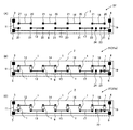
【解決手段】 LEDモジュール30が、平板状の絶縁基板2と、絶縁基板2の第1の端辺の近傍に形成された外部回路との接続用の第1主端子3と第1副端子5と、絶縁基板2の第1の端辺と対向する第2の端辺の近傍に形成された外部回路との接続用の第2主端子4と第2副端子6と、絶縁基板2上に形成され、相互に離間して連続的に配置されたLED1を直列接続するための3以上の連結用配線11〜19と、隣接する連結用配線間に各別に接続され同方向に直列接続した複数のLED1と、絶縁基板2上に形成され、第1副端子4と第2副端子6間を電気的に接続する第1通過配線8を備え、連結用配線の内の一方端側に位置する第1の連結用配線11が第1主端子3と接続し、連結用配線の内の他方端側に位置する第2の連結用配線19が第2主端子4と接続している。
【選択図】 図1
Description
図1に、本発明によるLEDモジュールの第1実施形態の概略構成を模式的に示す。図1(A)は、LEDを実装する前のプリント配線基板30’を示し、図1(B)は、LED1を実装後のLEDモジュール30を示す。
次に、本発明によるLEDモジュールの第2実施形態について説明する。図6に、本発明によるLEDモジュールの第2実施形態の概略構成を模式的に示す。図6(A)は、LEDを実装する前のプリント配線基板31’を示し、図6(B)は、LED1を実装後のLEDモジュール31(31a)を示し、図6(C)は、LED1と短絡用素子22を実装後のLEDモジュール31(31b)を示す。
次に、本発明によるLEDモジュールの第3実施形態について説明する。図9に、本発明によるLEDモジュールの第3実施形態の概略構成を模式的に示す。第2実施形態では、図6に示すように、電極23を連結用配線19(第2連結用配線に相当)と電気的に接続するように設け、第1通過配線8と電気的に接続する電極24と近接するように形成したが、第3実施形態では、図9に示すように、電極23を連結用配線11(第1連結用配線に相当)と電気的に接続するように設ける。図9(A)は、LEDを実装する前のプリント配線基板32’を示し、図9(B)は、LED1を実装後のLEDモジュール32(32a)を示し、図9(C)は、LED1と短絡用素子22を実装後のLEDモジュール32(32b)を示す。
次に、本発明によるLEDモジュールの第4実施形態について説明する。図12に、本発明によるLEDモジュールの第4実施形態の概略構成を模式的に示す。図12(A)は、LEDを実装する前のプリント配線基板33’を示し、図12(B)は、LED1を実装後のLEDモジュール33を示す。
次に、本発明によるLEDモジュールの第5実施形態について説明する。図15に、本発明によるLEDモジュールの第5実施形態の概略構成を模式的に示す。第4実施形態では、図12に示すように、第3副端子7を、第1主端子3及び第1副端子5と同じ側の端辺近傍に配置し、第2通過配線9を、第3副端子7と連結用配線19間を電気的に接続するように形成したが、第5実施形態では、図15に示すように、第3副端子7を、第2主端子4及び第2副端子6と同じ側の端辺近傍に配置し、第2通過配線9を第3副端子7と連結用配線11(第1連結用配線に相当)間を電気的に接続するように形成する。図15(A)は、LEDを実装する前のプリント配線基板34’を示し、図15(B)は、LED1を実装後のLEDモジュール34を示す。
次に、本発明によるLEDモジュールの第6実施形態について説明する。上記各実施形態では、9本の連結用配線11〜19と第1通過配線8を、絶縁基板2の同一面上に形成する場合について説明したが、連結用配線11〜19を絶縁基板2の一方の面上(例えば表面上)に形成し、第1通過配線8を他方の面上(例えば裏面上)に形成するのも好ましい。
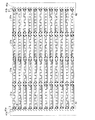
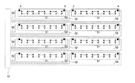
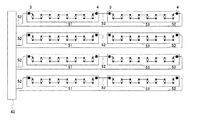
次に、本発明の第7実施形態として、上記各実施形態のLEDモジュール30〜36をマトリクス状に配列してLEDを面状に分散配置したLED光源装置について、図23を参照して説明する。図23では、LEDモジュールとして、第2実施形態のLEDモジュール31(31a、31b)を使用したケースについて例示するが、使用するLEDモジュールは、第2実施形態に限定されるものではない。
2: 絶縁基板
3: 第1主端子(アノード端子)
4: 第2主端子(カソード端子)
5: 第1副端子
6: 第2副端子
7: 第3副端子
8: 第1通過配線
9: 第2通過配線
11〜19: 連結用配線
20、21: LED接続用の電極
22: 短絡用の2端子素子
23、24: 短絡用の2端子素子接続用の電極
25: 第1貫通孔
26: 第2貫通孔
27: 突起部
30〜36: LEDモジュール
30’〜36’: プリント配線基板
37: LED列
37A: アノード端子
37C: カソード端子
38: 電流制限素子
41a〜41e: 外部配線
42: 制御基板
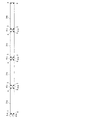
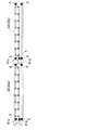
50、51: 従来のLEDモジュール
52: 外部配線
VH: 第1電源
VL: 第2電源
Claims (10)
- 平板状の絶縁基板と、
前記絶縁基板の第1の端辺の近傍に形成された外部回路との接続用の第1主端子と第1副端子と、
前記絶縁基板の前記第1の端辺と対向する第2の端辺の近傍に形成された外部回路との接続用の第2主端子と第2副端子と、
前記絶縁基板上に形成され、相互に離間して連続的に配置されたLEDを直列接続するための3以上の連結用配線と、
隣接する前記連結用配線間に各別に接続され同方向に直列接続した複数のLEDと、
前記絶縁基板上に形成され、前記第1副端子と前記第2副端子間を電気的に接続する第1通過配線と、を備え、
連続的に配置された前記3以上の連結用配線の内の一方端側に位置する1つの前記連結用配線である第1連結用配線が前記第1主端子と電気的に接続し、
連続的に配置された前記3以上の連結用配線の内の他方端側に位置する他の1つの前記連結用配線である第2連結用配線が前記第2主端子と電気的に接続していることを特徴とするLEDモジュール。 - 短絡用の2端子素子の各端子と接続するための1対の接続用電極が、前記絶縁基板上に形成され、
前記1対の接続用電極の一方が前記第1連結用配線または前記第2連結用配線と電気的に接続し、前記1対の接続用電極の他方が前記第1通過配線と電気的に接続していることを特徴とする請求項1に記載のLEDモジュール。 - 前記絶縁基板の前記第1の端辺の近傍に、外部回路との接続用の第3副端子が形成され、
前記絶縁基板上に、前記第2主端子または前記第2連結用配線と前記第3副端子間を電気的に接続する第2通過配線が形成されていることを特徴とする請求項1に記載のLEDモジュール。 - 前記絶縁基板の前記第2の端辺の近傍に、外部回路との接続用の第3副端子が形成され、
前記絶縁基板上に、前記第1主端子または前記第1連結用配線と前記第3副端子間を電気的に接続する第2通過配線が形成されていることを特徴とする請求項1に記載のLEDモジュール。 - 前記3以上の連結用配線が、前記絶縁基板の一方側の面上に形成され、
前記第1通過配線が、前記絶縁基板の他方側の面上に形成されていることを特徴とする請求項1〜4の何れか1項に記載のLEDモジュール。 - 前記第1主端子と前記第2主端子と前記3以上の連結用配線が、前記絶縁基板の一方側の面上に形成され、
前記第1副端子と前記第2副端子と前記第1通過配線が、前記絶縁基板の他方側の面上に形成されていることを特徴とする請求項1または2に記載のLEDモジュール。 - 前記第1通過配線が前記絶縁基板の両方の面上に形成され、
前記絶縁基板の一方側の面上に形成された前記第1通過配線と、前記絶縁基板の他方側の面上に形成された前記第1通過配線が、前記絶縁基板に複数形成された内壁面が金属で被覆された貫通孔を介して電気的に接続していることを特徴とする請求項5または6に記載のLEDモジュール。 - 前記絶縁基板の他方側の面上に形成された前記第1通過配線が、前記絶縁基板の内部に向けて突出する突起部を備えていることを特徴とする5〜7の何れか1項に記載のLEDモジュール。
- 前記絶縁基板に内壁面が金属で被覆された貫通孔が複数形成されていることを特徴とする1〜6の何れか1項に記載のLEDモジュール。
- 請求項1〜9の何れか1項に記載のLEDモジュールを、1つの前記LEDモジュールの前記第1の端辺と、他の1つの前記LEDモジュールの前記第2の端辺を近接させて第1方向に複数配列し、近接する前記第1の端辺の近傍に配置された前記主端子の1つと前記第2の端辺の近傍に配置された前記主端子の1つを電気的に接続し、近接する前記第1の端辺の近傍に配置された前記副端子の1つと前記第2の端辺の近傍に配置された前記副端子の1つを電気的に接続してLEDモジュール列を構成し、
前記LEDモジュール列を、前記第1方向と直交する第2方向に複数配列して、前記LEDモジュールに実装されている前記LEDを面状に複数配列することを特徴とするLED光源装置。
Priority Applications (4)
| Application Number | Priority Date | Filing Date | Title |
|---|---|---|---|
| JP2009045120A JP4801751B2 (ja) | 2009-02-27 | 2009-02-27 | Ledモジュール及びled光源装置 |
| US12/659,106 US8403532B2 (en) | 2009-02-27 | 2010-02-25 | LED module and LED light source apparatus |
| KR1020100018013A KR101157852B1 (ko) | 2009-02-27 | 2010-02-26 | Led 모듈 및 led 광원 장치 |
| CN2010101262130A CN101819967B (zh) | 2009-02-27 | 2010-02-26 | Led模块以及led光源装置 |
Applications Claiming Priority (1)
| Application Number | Priority Date | Filing Date | Title |
|---|---|---|---|
| JP2009045120A JP4801751B2 (ja) | 2009-02-27 | 2009-02-27 | Ledモジュール及びled光源装置 |
Related Child Applications (1)
| Application Number | Title | Priority Date | Filing Date |
|---|---|---|---|
| JP2011054456A Division JP5204864B2 (ja) | 2011-03-11 | 2011-03-11 | Ledモジュール及びled光源装置 |
Publications (2)
| Publication Number | Publication Date |
|---|---|
| JP2010199005A true JP2010199005A (ja) | 2010-09-09 |
| JP4801751B2 JP4801751B2 (ja) | 2011-10-26 |
Family
ID=42654992
Family Applications (1)
| Application Number | Title | Priority Date | Filing Date |
|---|---|---|---|
| JP2009045120A Expired - Fee Related JP4801751B2 (ja) | 2009-02-27 | 2009-02-27 | Ledモジュール及びled光源装置 |
Country Status (4)
| Country | Link |
|---|---|
| US (1) | US8403532B2 (ja) |
| JP (1) | JP4801751B2 (ja) |
| KR (1) | KR101157852B1 (ja) |
| CN (1) | CN101819967B (ja) |
Cited By (10)
| Publication number | Priority date | Publication date | Assignee | Title |
|---|---|---|---|---|
| WO2012128074A1 (ja) * | 2011-03-18 | 2012-09-27 | シャープ株式会社 | 照明装置、表示装置、及びテレビ受信装置 |
| JP2013143275A (ja) * | 2012-01-11 | 2013-07-22 | Sharp Corp | 照明装置、表示装置、及びテレビ受信装置 |
| JP2013543207A (ja) * | 2010-08-30 | 2013-11-28 | オスラム オプト セミコンダクターズ ゲゼルシャフト ミット ベシュレンクテル ハフツング | プリント回路基板上の光源デバイスおよび複数の光源デバイスを備えた光源装置 |
| JP5416293B1 (ja) * | 2013-02-27 | 2014-02-12 | アイリスオーヤマ株式会社 | 照明装置 |
| JP2014089817A (ja) * | 2012-10-29 | 2014-05-15 | Rohm Co Ltd | 照明器具および照明器具の製造方法 |
| JP2014528171A (ja) * | 2011-09-16 | 2014-10-23 | エアー・モーション・システムズ・インコーポレイテッドAir Motion Systems, Inc. | 高出力led装置の組立及び相互接続の方法 |
| JP2014206641A (ja) * | 2013-04-12 | 2014-10-30 | 船井電機株式会社 | 表示装置およびバックライト |
| JP2017167548A (ja) * | 2017-04-25 | 2017-09-21 | 船井電機株式会社 | 表示装置 |
| EP3381349A1 (en) | 2017-03-29 | 2018-10-03 | Hoya Candeo Optronics Corporation | Light emitting device and light illuminating apparatus comprising the light emitting device |
| KR20230000089A (ko) * | 2021-06-24 | 2023-01-02 | 주식회사 루멘스 | Led용 pcb 기판 및 pcb 조립체 |
Families Citing this family (32)
| Publication number | Priority date | Publication date | Assignee | Title |
|---|---|---|---|---|
| US8308320B2 (en) | 2009-11-12 | 2012-11-13 | Cooper Technologies Company | Light emitting diode modules with male/female features for end-to-end coupling |
| KR101709082B1 (ko) * | 2010-03-16 | 2017-02-23 | 삼성디스플레이 주식회사 | 발광 소자를 포함하는 회로 기판 및 표시장치 |
| US8616720B2 (en) | 2010-04-27 | 2013-12-31 | Cooper Technologies Company | Linkable linear light emitting diode system |
| WO2011139768A2 (en) * | 2010-04-28 | 2011-11-10 | Cooper Technologies Company | Linear led light module |
| JP5612991B2 (ja) | 2010-09-30 | 2014-10-22 | シャープ株式会社 | 発光装置及びこれを備えた照明装置 |
| WO2012144126A1 (ja) * | 2011-04-20 | 2012-10-26 | パナソニック株式会社 | 発光装置、バックライトユニット、液晶表示装置及び照明装置 |
| JP2012244018A (ja) * | 2011-05-20 | 2012-12-10 | Toshiba Lighting & Technology Corp | 発光モジュール及び照明器具 |
| CN202217702U (zh) * | 2011-07-01 | 2012-05-09 | 方与圆电子(深圳)有限公司 | 一种光源模组及照明装置 |
| CN102881810B (zh) * | 2011-07-13 | 2016-06-22 | 李学旻 | 发光源装置 |
| TWI464339B (zh) * | 2012-03-03 | 2014-12-11 | Lextar Electronics Corp | 發光二極體燈條及應用其之發光二極體模組 |
| EP2658000B1 (en) * | 2012-03-13 | 2018-05-02 | Panasonic Intellectual Property Management Co., Ltd. | Substrate, light-emitting device, and illumination device |
| CN102661496B (zh) * | 2012-04-09 | 2015-06-17 | 深圳市华星光电技术有限公司 | Led光源及相应的背光模块 |
| CN103219331A (zh) * | 2012-09-13 | 2013-07-24 | 天津金玛光电有限公司 | 单向hv led芯片 |
| US9215792B2 (en) | 2013-03-15 | 2015-12-15 | Cree, Inc. | Connector devices, systems, and related methods for light emitter components |
| US9897267B2 (en) * | 2013-03-15 | 2018-02-20 | Cree, Inc. | Light emitter components, systems, and related methods |
| DE102013208392A1 (de) * | 2013-05-07 | 2014-11-13 | Osram Gmbh | LED-Modul und Leuchte mit einem LED-Modul |
| KR102108214B1 (ko) * | 2013-06-12 | 2020-05-07 | 엘지디스플레이 주식회사 | 발광다이오드어셈블리 및 그를 포함한 액정표시장치 |
| US8684750B1 (en) * | 2013-07-29 | 2014-04-01 | Chia-Yen Lin | Contact type of electric connection building block and electric connection unit disposed therein |
| DE202013105360U1 (de) * | 2013-11-25 | 2015-02-26 | Dewertokin Gmbh | Beleuchtungseinrichtung zur Verwendung mit einem elektromotorischen Möbelantrieb |
| CN105098013A (zh) * | 2014-05-15 | 2015-11-25 | 中国科学院苏州纳米技术与纳米仿生研究所 | 一种高压led发光器件 |
| AT14221U1 (de) * | 2014-05-19 | 2015-06-15 | Tridonic Gmbh & Co Kg | Leuchtmittel mit LED und Verfahren zur Montage |
| KR102231646B1 (ko) * | 2014-10-17 | 2021-03-24 | 엘지이노텍 주식회사 | 발광 소자 |
| TWI570352B (zh) * | 2014-11-28 | 2017-02-11 | 宏齊科技股份有限公司 | 發光二極體裝置與應用其之發光裝置 |
| CN104456249B (zh) * | 2014-12-01 | 2017-09-12 | 深圳市熠鸿光电科技有限公司 | Led光源模组 |
| US9989223B1 (en) * | 2015-03-09 | 2018-06-05 | Automated Assembly Corporation | LED lighting apparatus with LEDs and wires attached to metal sheet member by adhesive |
| WO2016168318A1 (en) | 2015-04-13 | 2016-10-20 | Hubbell Incorporated | Light board |
| DE102017109853A1 (de) * | 2017-05-08 | 2018-11-08 | Ledvance Gmbh | Halbleiter-Light Engine für eine Röhrenlampe |
| CN108036204B (zh) * | 2017-12-14 | 2020-03-17 | 广东雷腾智能光电有限公司 | 一种消除杂光的cob光源 |
| DE102019104792A1 (de) * | 2018-03-01 | 2019-09-05 | Nichia Corporation | Lichtemittierendes modul |
| KR102902146B1 (ko) * | 2021-08-31 | 2025-12-19 | 삼성전자주식회사 | 발광 다이오드 모듈 및 이를 포함하는 디스플레이 장치 |
| EP4287260A4 (en) | 2021-08-31 | 2024-10-09 | Samsung Electronics Co., Ltd. | LIGHT EMITTING DIODE MODULE AND DISPLAY DEVICE COMPRISING SAME |
| WO2025082788A1 (en) * | 2023-10-20 | 2025-04-24 | Signify Holding B.V. | Lamp |
Citations (4)
| Publication number | Priority date | Publication date | Assignee | Title |
|---|---|---|---|---|
| JP2007026858A (ja) * | 2005-07-15 | 2007-02-01 | Minebea Co Ltd | 面状照明装置 |
| JP2007201334A (ja) * | 2006-01-30 | 2007-08-09 | Kyocera Corp | 発光装置および照明装置 |
| JP2007305512A (ja) * | 2006-05-15 | 2007-11-22 | Yamatake Corp | Led照明装置 |
| WO2008090643A1 (ja) * | 2007-01-22 | 2008-07-31 | Sharp Kabushiki Kaisha | 光源モジュール及びバックライト光源 |
Family Cites Families (10)
| Publication number | Priority date | Publication date | Assignee | Title |
|---|---|---|---|---|
| JPS6234468A (ja) | 1985-08-07 | 1987-02-14 | Nec Corp | 画信号補正装置 |
| EP1204144A1 (en) * | 2000-11-06 | 2002-05-08 | Jaenam Kim | Led lamp apparatus |
| JP4028985B2 (ja) | 2002-01-16 | 2008-01-09 | ハリソン東芝ライティング株式会社 | バックライトユニット |
| CN2550905Y (zh) * | 2002-05-22 | 2003-05-14 | 光鼎电子股份有限公司 | 发光二极管晶片的串联结构 |
| US7111961B2 (en) * | 2002-11-19 | 2006-09-26 | Automatic Power, Inc. | High flux LED lighting device |
| JP2005079161A (ja) * | 2003-08-28 | 2005-03-24 | Osram-Melco Ltd | 発光ダイオードモジュール及び発光ダイオードモジュールの製造方法及び発光ダイオードモジュールの使用方法 |
| CN2927319Y (zh) * | 2006-06-20 | 2007-07-25 | 楼满娥 | 用于安装led芯片的电连接装置 |
| JP2008053062A (ja) | 2006-08-24 | 2008-03-06 | Sony Corp | バックライト装置及び液晶表示装置 |
| KR100974923B1 (ko) * | 2007-03-19 | 2010-08-10 | 서울옵토디바이스주식회사 | 발광 다이오드 |
| JP3139714U (ja) * | 2007-12-10 | 2008-02-28 | 鳥海工業株式会社 | Ledランプ |
-
2009
- 2009-02-27 JP JP2009045120A patent/JP4801751B2/ja not_active Expired - Fee Related
-
2010
- 2010-02-25 US US12/659,106 patent/US8403532B2/en not_active Expired - Fee Related
- 2010-02-26 CN CN2010101262130A patent/CN101819967B/zh not_active Expired - Fee Related
- 2010-02-26 KR KR1020100018013A patent/KR101157852B1/ko not_active Expired - Fee Related
Patent Citations (4)
| Publication number | Priority date | Publication date | Assignee | Title |
|---|---|---|---|---|
| JP2007026858A (ja) * | 2005-07-15 | 2007-02-01 | Minebea Co Ltd | 面状照明装置 |
| JP2007201334A (ja) * | 2006-01-30 | 2007-08-09 | Kyocera Corp | 発光装置および照明装置 |
| JP2007305512A (ja) * | 2006-05-15 | 2007-11-22 | Yamatake Corp | Led照明装置 |
| WO2008090643A1 (ja) * | 2007-01-22 | 2008-07-31 | Sharp Kabushiki Kaisha | 光源モジュール及びバックライト光源 |
Cited By (13)
| Publication number | Priority date | Publication date | Assignee | Title |
|---|---|---|---|---|
| US9097414B2 (en) | 2010-08-30 | 2015-08-04 | Osram Oled Gmbh | Light source device on a printed circuit board and light source arrangement comprising a plurality of light source devices |
| JP2013543207A (ja) * | 2010-08-30 | 2013-11-28 | オスラム オプト セミコンダクターズ ゲゼルシャフト ミット ベシュレンクテル ハフツング | プリント回路基板上の光源デバイスおよび複数の光源デバイスを備えた光源装置 |
| WO2012128074A1 (ja) * | 2011-03-18 | 2012-09-27 | シャープ株式会社 | 照明装置、表示装置、及びテレビ受信装置 |
| JP2014528171A (ja) * | 2011-09-16 | 2014-10-23 | エアー・モーション・システムズ・インコーポレイテッドAir Motion Systems, Inc. | 高出力led装置の組立及び相互接続の方法 |
| JP2013143275A (ja) * | 2012-01-11 | 2013-07-22 | Sharp Corp | 照明装置、表示装置、及びテレビ受信装置 |
| JP2014089817A (ja) * | 2012-10-29 | 2014-05-15 | Rohm Co Ltd | 照明器具および照明器具の製造方法 |
| JP5416293B1 (ja) * | 2013-02-27 | 2014-02-12 | アイリスオーヤマ株式会社 | 照明装置 |
| JP2014206641A (ja) * | 2013-04-12 | 2014-10-30 | 船井電機株式会社 | 表示装置およびバックライト |
| EP3381349A1 (en) | 2017-03-29 | 2018-10-03 | Hoya Candeo Optronics Corporation | Light emitting device and light illuminating apparatus comprising the light emitting device |
| US10362642B2 (en) | 2017-03-29 | 2019-07-23 | Hoya Candeo Optronics Corporation | Light emitting device and light illuminating apparatus comprising the light emitting device |
| JP2017167548A (ja) * | 2017-04-25 | 2017-09-21 | 船井電機株式会社 | 表示装置 |
| KR20230000089A (ko) * | 2021-06-24 | 2023-01-02 | 주식회사 루멘스 | Led용 pcb 기판 및 pcb 조립체 |
| KR102561717B1 (ko) * | 2021-06-24 | 2023-08-02 | 주식회사 루멘스 | Led용 pcb 기판 및 pcb 조립체 |
Also Published As
| Publication number | Publication date |
|---|---|
| US20100220479A1 (en) | 2010-09-02 |
| US8403532B2 (en) | 2013-03-26 |
| CN101819967B (zh) | 2012-08-15 |
| CN101819967A (zh) | 2010-09-01 |
| KR20100098340A (ko) | 2010-09-06 |
| KR101157852B1 (ko) | 2012-06-22 |
| JP4801751B2 (ja) | 2011-10-26 |
Similar Documents
| Publication | Publication Date | Title |
|---|---|---|
| JP4801751B2 (ja) | Ledモジュール及びled光源装置 | |
| JP5204864B2 (ja) | Ledモジュール及びled光源装置 | |
| CN207852672U (zh) | 一种四连体rgb-led封装模组及其显示屏 | |
| US8222653B2 (en) | Light-emitting diode and lighting apparatus using the same | |
| JP5545848B2 (ja) | 半導体発光装置 | |
| US20200154564A1 (en) | Light-emitting module | |
| CN101826593B (zh) | 有助于减小发光设备的厚度并且具有高通用性的布线板 | |
| CN114280841B (zh) | 一种发光基板及显示装置 | |
| JP2008258264A (ja) | 光源ユニット用発光ダイオードモジュールの構造 | |
| JP7605823B2 (ja) | 発光板、回路基板及び表示装置 | |
| US9313835B2 (en) | Planar light emitting device | |
| JP5711240B2 (ja) | 光源モジュール及び発光デバイス | |
| KR101017921B1 (ko) | 발광 소자 실장용 기판, 발광 모듈 및 조명 장치 | |
| JP2011018695A (ja) | 発光装置およびその製造方法 | |
| CN110133912A (zh) | 一种led背光器件及背光模组 | |
| CN112268237B (zh) | 一种多基色无光斑柔性灯带 | |
| CN215182844U (zh) | 显示装置及其灯板 | |
| JP3884057B2 (ja) | 発光素子実装用基板、発光モジュール及び照明装置 | |
| CN216213535U (zh) | 一种灯丝结构及装饰灯 | |
| JP4628877B2 (ja) | 発光素子実装用ホーロー基板、発光素子モジュール、照明装置、表示装置及び交通信号機 | |
| JP5328960B2 (ja) | Ledランプ | |
| JP5910174B2 (ja) | 照明装置 | |
| TWI420959B (zh) | 發光二極體模組 | |
| CN119007589A (zh) | 显示面板拼接单元及其所拼接的显示面板 | |
| CN102454878A (zh) | 发光二极管模组 |
Legal Events
| Date | Code | Title | Description |
|---|---|---|---|
| A977 | Report on retrieval |
Free format text: JAPANESE INTERMEDIATE CODE: A971007 Effective date: 20101216 |
|
| A131 | Notification of reasons for refusal |
Free format text: JAPANESE INTERMEDIATE CODE: A131 Effective date: 20110118 |
|
| A521 | Request for written amendment filed |
Free format text: JAPANESE INTERMEDIATE CODE: A523 Effective date: 20110311 |
|
| A131 | Notification of reasons for refusal |
Free format text: JAPANESE INTERMEDIATE CODE: A131 Effective date: 20110419 |
|
| A521 | Request for written amendment filed |
Free format text: JAPANESE INTERMEDIATE CODE: A523 Effective date: 20110610 |
|
| TRDD | Decision of grant or rejection written | ||
| A01 | Written decision to grant a patent or to grant a registration (utility model) |
Free format text: JAPANESE INTERMEDIATE CODE: A01 Effective date: 20110712 |
|
| A01 | Written decision to grant a patent or to grant a registration (utility model) |
Free format text: JAPANESE INTERMEDIATE CODE: A01 |
|
| A61 | First payment of annual fees (during grant procedure) |
Free format text: JAPANESE INTERMEDIATE CODE: A61 Effective date: 20110805 |
|
| FPAY | Renewal fee payment (event date is renewal date of database) |
Free format text: PAYMENT UNTIL: 20140812 Year of fee payment: 3 |
|
| R150 | Certificate of patent or registration of utility model |
Ref document number: 4801751 Country of ref document: JP Free format text: JAPANESE INTERMEDIATE CODE: R150 Free format text: JAPANESE INTERMEDIATE CODE: R150 |
|
| LAPS | Cancellation because of no payment of annual fees |