WO2012128270A1 - 発光素子用台座基板およびledデバイス - Google Patents
発光素子用台座基板およびledデバイス Download PDFInfo
- Publication number
- WO2012128270A1 WO2012128270A1 PCT/JP2012/057121 JP2012057121W WO2012128270A1 WO 2012128270 A1 WO2012128270 A1 WO 2012128270A1 JP 2012057121 W JP2012057121 W JP 2012057121W WO 2012128270 A1 WO2012128270 A1 WO 2012128270A1
- Authority
- WO
- WIPO (PCT)
- Prior art keywords
- substrate
- light emitting
- base
- emitting element
- individual
- Prior art date
- Legal status (The legal status is an assumption and is not a legal conclusion. Google has not performed a legal analysis and makes no representation as to the accuracy of the status listed.)
- Ceased
Links
Images


Classifications
-
- H—ELECTRICITY
- H10—SEMICONDUCTOR DEVICES; ELECTRIC SOLID-STATE DEVICES NOT OTHERWISE PROVIDED FOR
- H10H—INORGANIC LIGHT-EMITTING SEMICONDUCTOR DEVICES HAVING POTENTIAL BARRIERS
- H10H20/00—Individual inorganic light-emitting semiconductor devices having potential barriers, e.g. light-emitting diodes [LED]
- H10H20/80—Constructional details
- H10H20/85—Packages
- H10H20/857—Interconnections, e.g. lead-frames, bond wires or solder balls
-
- H—ELECTRICITY
- H10—SEMICONDUCTOR DEVICES; ELECTRIC SOLID-STATE DEVICES NOT OTHERWISE PROVIDED FOR
- H10H—INORGANIC LIGHT-EMITTING SEMICONDUCTOR DEVICES HAVING POTENTIAL BARRIERS
- H10H29/00—Integrated devices, or assemblies of multiple devices, comprising at least one light-emitting semiconductor element covered by group H10H20/00
- H10H29/10—Integrated devices comprising at least one light-emitting semiconductor component covered by group H10H20/00
- H10H29/14—Integrated devices comprising at least one light-emitting semiconductor component covered by group H10H20/00 comprising multiple light-emitting semiconductor components
- H10H29/142—Two-dimensional arrangements, e.g. asymmetric LED layout
-
- H—ELECTRICITY
- H10—SEMICONDUCTOR DEVICES; ELECTRIC SOLID-STATE DEVICES NOT OTHERWISE PROVIDED FOR
- H10D—INORGANIC ELECTRIC SEMICONDUCTOR DEVICES
- H10D89/00—Aspects of integrated devices not covered by groups H10D84/00 - H10D88/00
- H10D89/60—Integrated devices comprising arrangements for electrical or thermal protection, e.g. protection circuits against electrostatic discharge [ESD]
-
- H—ELECTRICITY
- H10—SEMICONDUCTOR DEVICES; ELECTRIC SOLID-STATE DEVICES NOT OTHERWISE PROVIDED FOR
- H10H—INORGANIC LIGHT-EMITTING SEMICONDUCTOR DEVICES HAVING POTENTIAL BARRIERS
- H10H20/00—Individual inorganic light-emitting semiconductor devices having potential barriers, e.g. light-emitting diodes [LED]
- H10H20/80—Constructional details
- H10H20/85—Packages
- H10H20/8506—Containers
-
- H—ELECTRICITY
- H10—SEMICONDUCTOR DEVICES; ELECTRIC SOLID-STATE DEVICES NOT OTHERWISE PROVIDED FOR
- H10W—GENERIC PACKAGES, INTERCONNECTIONS, CONNECTORS OR OTHER CONSTRUCTIONAL DETAILS OF DEVICES COVERED BY CLASS H10
- H10W72/00—Interconnections or connectors in packages
- H10W72/071—Connecting or disconnecting
- H10W72/072—Connecting or disconnecting of bump connectors
- H10W72/07251—Connecting or disconnecting of bump connectors characterised by changes in properties of the bump connectors during connecting
-
- H—ELECTRICITY
- H10—SEMICONDUCTOR DEVICES; ELECTRIC SOLID-STATE DEVICES NOT OTHERWISE PROVIDED FOR
- H10W—GENERIC PACKAGES, INTERCONNECTIONS, CONNECTORS OR OTHER CONSTRUCTIONAL DETAILS OF DEVICES COVERED BY CLASS H10
- H10W72/00—Interconnections or connectors in packages
- H10W72/20—Bump connectors, e.g. solder bumps or copper pillars; Dummy bumps; Thermal bumps
-
- H—ELECTRICITY
- H10—SEMICONDUCTOR DEVICES; ELECTRIC SOLID-STATE DEVICES NOT OTHERWISE PROVIDED FOR
- H10W—GENERIC PACKAGES, INTERCONNECTIONS, CONNECTORS OR OTHER CONSTRUCTIONAL DETAILS OF DEVICES COVERED BY CLASS H10
- H10W90/00—Package configurations
Definitions
- the present invention relates to a light-emitting element base substrate for mounting and mounting a light-emitting element on a surface, and an LED device including the light-emitting element base substrate.
- LEDs Light Emitting Diodes
- LED devices that are currently in practical use are generally of the following structure.
- a three-color light-emitting element having a color close to the three primary colors of light is mounted on a single light-emitting element base substrate, and the surface is covered with a protective translucent sealing resin.
- a blue or near ultraviolet light emitting element is mounted on a light emitting element base substrate, and the light emitting element is covered with a sealing resin containing a fluorescent or phosphorescent substance.
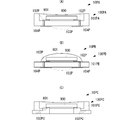
- FIG. 1A, 1B, and 1C are side cross-sectional views illustrating a typical structure example of a conventional LED device.
- the light-emitting element base substrate 100PA includes a box-shaped base body 101PA having a recess composed of a bottom plate and a side wall formed along the outer periphery of the bottom plate.
- the base 101PA is made of an insulating ceramic.
- a mounting electrode 102P for mounting the light emitting element 900 is formed on the surface of the bottom plate of the base 101PA on the concave side.
- An external connection electrode 103P is formed on the surface of the bottom plate of the base 101PA opposite to the concave side.
- a via electrode 104P that electrically connects the mounting electrode 102P and the external connection electrode 103P is formed on the bottom plate of the base 101PA.
- the substrate 101PA, the mounting electrode 102P, the external connection electrode 103P, and the via electrode 104P constitute a light emitting element base substrate 100PA.
- the light emitting element 900 is disposed in the recess of the base 101PA and mounted on the mounting electrode 102P. This recess is filled with a sealing resin 901. For this reason, the light emitting element 900 is covered with the sealing resin 901.
- the 1B includes a light emitting element 900 and a light emitting element base substrate 100PB.
- the light emitting element base substrate 100PB includes a flat substrate 101PB.
- a mounting electrode 102P for mounting the light emitting element 900 is formed on the surface of the base 101PB.
- An external connection electrode 103P is formed on the back surface of the base 101PB.
- a via electrode 104P that electrically connects the mounting electrode 102P and the external connection electrode 103P is formed on the base 101PB.
- the base 101PB, the mounting electrode 102P, the external connection electrode 103P, and the via electrode 104P constitute a light emitting element base substrate 100PB.
- the light emitting element 900 is disposed on the surface of the base 101PB and mounted on the mounting electrode 102P.
- a sealing resin 901 is provided on the surface of the light emitting element base substrate 100PB so as to cover the light emitting element 900.
- the 1C includes a light emitting element 900 and a light emitting element base substrate 100PC.
- the light emitting element base substrate 100PC includes a box-shaped base body 101PC having a recess composed of a bottom plate and a side wall formed along the outer periphery of the bottom plate.
- the base 101PC is made of a heat resistant resin.
- a mounting electrode 102PC for mounting the light emitting element 900 exposed on the surface on the concave side and the surface on the opposite side to the concave side is disposed.
- the base 101PC and the mounting electrode 102PC constitute a light emitting element base substrate 100PC.
- the light emitting element 900 is disposed in the recess of the base 101PC and is mounted on the mounting electrode 102PC. This recess is filled with a sealing resin 901. For this reason, the light emitting element 900 is covered with the sealing resin 901.
- Patent Document 1 discloses a silicon semiconductor substrate having good heat dissipation characteristics, A metal substrate is used as the base of the light emitting element base substrate.
- an LED device provided with an ESD protection element to prevent electrostatic breakdown of the light emitting element.
- a base of a light emitting element base substrate is formed of a semiconductor substrate, and an ESD protection element is formed in the semiconductor substrate.
- the mounting electrode to which the two terminals of the light-emitting element are connected must be insulated.
- the silicon substrate must be electrically separated into two regions.
- an insulating layer for insulation isolation is formed linearly in the vicinity of the center of the low-resistance silicon substrate. Specifically, for example, an insulating layer made of a silicon oxide layer is formed on a low resistance silicon substrate.
- the silicon oxide layer is weaker in mechanical strength than silicon, tends to cause peeling at the interface between the silicon and the silicon oxide layer, and is inferior in reliability.
- a via electrode for connecting the mounting electrode for mounting the light-emitting element and the external connection electrode for mounting the LED device on the external circuit board must be provided.
- the manufacturing process may increase and the manufacturing cost may increase.
- An object of the present invention is to realize a light emitting element pedestal substrate having excellent heat dissipation and high mechanical strength by a relatively simple manufacturing process, and an LED device including the light emitting element pedestal substrate.
- a base substrate for a light emitting element according to the present invention includes a base made of a low-resistance semiconductor substrate, an insulating layer that divides the base into a first individual base and a second individual base, and a first individual base.
- the first surface side mounting electrode provided on the surface of the first surface, the first external connection electrode provided on the back surface of the first individual substrate, and the second surface side mounting electrode provided on the surface of the second individual substrate And a second external connection electrode provided on the back surface of the second individual substrate.
- the insulating layer has a shape different from the straight line shape in plan view.
- one terminal of the light emitting element is connected to the first surface side mounting electrode, and the other terminal of the light emitting element is connected to the second surface side mounting electrode.
- the substrate is made of a low-resistance semiconductor substrate
- the first surface-side mounting electrode formed on the first individual substrate and the first external connection electrode are electrically connected to each other, and the second surface formed on the second individual substrate 2
- the front surface mounting electrode and the second external connection electrode are electrically connected.
- the first individual substrate and the second individual substrate are insulated by the insulating layer, the first surface-side mounting electrode and the second surface-side mounting electrode are not electrically connected.
- the first external connection electrode, the first individual substrate, the first surface side mounting electrode, the light emitting element, the second surface side mounting electrode, the second individual substrate, and the second external connection electrode are electrically connected.
- the signal is transmitted with low loss.
- heat dissipation is high by using a semiconductor substrate for the base.
- the insulating layer is not straight, and for example, as shown in FIG. 2, the individual portions extending in a plurality of directions that are not parallel to each other are continuously connected. Even if bending stress is applied, the stress related to the insulating layer becomes compressive stress. Therefore, it is possible to prevent the occurrence of breakage at the interface between the insulating layer or the insulating layer and the first individual base and the second individual base.
- the pedestal substrate for a light emitting device of the present invention includes an electrostatic breakdown preventing layer provided on the surface of the first individual substrate.
- the base substrate for light emitting element has an ESD protection function. Further, in this configuration, since the electrostatic breakdown prevention layer is provided on the surface of the first individual base body, it is possible to manufacture by an easier manufacturing process than when the electrostatic breakdown prevention layer is formed in the base body as in the past. become.
- the second surface side mounting electrode is provided so as to reach the surface of the first individual substrate, and the electrostatic breakdown preventing layer has a second surface in plan view. It is preferable that it is provided between the second surface side mounting electrode and the surface of the first individual substrate so that the whole overlaps with the side mounting electrode.
- the electrostatic breakdown preventing layer can be protected from the external environment. Thereby, ESD characteristic deterioration of the electrostatic breakdown preventing layer due to the external environment (continuous light irradiation or the like) can be prevented.
- the electrostatic breakdown preventing layer is preferably a semiconductor layer having majority carriers having a polarity opposite to that of the substrate.
- This configuration shows an example of an electrostatic breakdown preventing layer.
- a p-type silicon layer is formed as an electrostatic breakdown preventing layer.
- a pn junction is realized at the interface between the electrostatic breakdown preventing layer and the semiconductor substrate, and functions as an ESD protection element.
- the electrostatic breakdown preventing layer is preferably a varistor layer.
- a varistor layer is formed of a metal oxide film or a positive temperature coefficient thermistor element having a varistor characteristic that has a high resistance at a predetermined voltage or lower and a low resistance when a predetermined voltage is exceeded. Can be configured. Even with this configuration, an ESD protection element can be realized.
- the electrostatic breakdown preventing layer is preferably a low-concentration semiconductor layer having the same polarity as the base and having a lower concentration carrier than the base.
- This configuration shows an example of an electrostatic breakdown prevention layer.
- a low-concentration semiconductor layer that is an n-type silicon layer having a low carrier concentration is formed as an electrostatic breakdown prevention layer. To do.
- a Schottky barrier diode is realized by the electrostatic breakdown preventing layer and the substrate, and functions as an ESD protection element.
- the light emitting element base substrate of the present invention includes a side insulating layer provided on the outer surface of the base.
- the 1st surface side mounting electrode and the 2nd surface side mounting electrode and a base
- the metal that forms the first surface-side mounting electrode and the second surface-side mounting electrode can be prevented from thermally diffusing into the substrate, and the aging deterioration occurs when the light-emitting element continues to emit light. Can be prevented.
- the surface of the base is provided with a surface-side insulating layer in which at least a part of the first surface-side mounting electrode and the second surface-side mounting electrode is a non-formation region. It is preferable.
- the insulating layer is formed except for the portion where the light emitting element is electrically connected to the surface of the substrate, external factors such as dew condensation or a bonding member (when the light emitting element is mounted on the semiconductor substrate ( A short circuit between the first individual base and the second individual base due to a solder material such as solder can be prevented.
- the back surface side insulating layer in which at least a part of the first external connection electrode and the second external connection electrode is not formed is provided on the back surface of the base. It is preferable.
- the insulating layer is formed except for the portion connected to the external circuit board on the back surface of the base body, external factors such as dew condensation or when the light emitting element base board is mounted on the external circuit board A short circuit between the first individual base and the second individual base due to the joining member (wax material such as solder) can be prevented.
- an LED device comprising: the above-described pedestal substrate for a light emitting element; and a light emitting element in which an anode electrode and a cathode electrode are connected to the first surface side mounting electrode and the second surface side mounting electrode, respectively.
- the present invention also relates to a light emitting element base substrate used for connecting a plurality of light emitting elements to an external circuit board.
- the base substrate for a light emitting element includes a base made of a low-resistance semiconductor substrate, an insulating layer that divides the base into at least a first individual base, a second individual base, and a third individual base that are insulated from each other, Is provided.
- the base substrate for light emitting element includes a first surface-side mounting electrode provided on the surface of the first individual substrate, a first external connection electrode provided on the back surface of the first individual substrate, and a surface of the second individual substrate.
- substrates in an insulating layer is a shape different from a straight line shape in planar view.
- the configuration of the light emitting element base substrate in which the single light emitting element is connected to the external circuit board is applied to the light emitting element base substrate in which a plurality of light emitting elements are connected to the external circuit board.
- the surface of the first individual base is provided with the first electrostatic breakdown preventing layer connected to the common surface side mounting electrode, and the surface of the second individual base is common. It is preferable to provide the 2nd electrostatic breakdown prevention layer connected to the surface side mounting electrode.
- the light emitting element base substrate of the present invention includes a side insulating layer provided on the outer surface of the base.
- the light emitting element base substrate and the first terminal are connected to the common surface side mounting electrode, and the second terminal is connected to each surface side mounting electrode other than the common surface side mounting electrode.
- An LED device is realized by including a plurality of connected light emitting elements.
- the LED device by using the light emitting element base substrate having the above-described configuration, it is possible to realize an LED device including a plurality of light emitting elements that is easy in manufacturing process and excellent in characteristics and reliability. At this time, the LED device can be miniaturized by using a common individual substrate and a surface-side mounting electrode.
- the present invention it is possible to realize a pedestal substrate for a light-emitting element having excellent heat dissipation and high mechanical strength by a relatively simple manufacturing process. And the LED device excellent in reliability is realizable by using the said base board for light emitting elements.
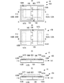
- FIG. 4 is a top view, bottom plan view, AA sectional view, and BB sectional view of the LED device 10 according to the first embodiment of the present invention.
- FIG. 3 is a side cross-sectional view taken along the line AA for explaining a manufacturing process of the light emitting element base substrate 100 of the LED device 10 according to the first embodiment of the present invention (first half).
- FIG. 4 is a side cross-sectional view of the above-mentioned AA cross-section for explaining a manufacturing process of the light-emitting element base substrate 100 of the LED device 10 according to the first embodiment of the present invention (second half).
- FIG. 7 is a plan view of the top surface of LED devices 10A to 10C according to first to third modifications of the present invention. It is an LED device which concerns on the 3rd Embodiment of this invention, Comprising: It is a figure which shows the structural example of LED device 10D, 10E which mounted two light emitting elements on the single base board for light emitting elements. It is an LED device which concerns on the 3rd Embodiment of this invention, Comprising: It is a figure which shows the structural example of LED device 10F which mounted three light emitting elements on the single base board for light emitting elements.
- FIG. 2 (A) is a plan view of the top surface of the LED device 10 according to the first embodiment of the present invention
- FIG. 2 (B) is a plan view of the bottom surface
- 2C is a cross-sectional view taken along line AA shown in FIGS. 2A and 2B
- FIG. 2D is a cross-sectional view taken along line BB shown in FIGS. 2A and 2B. is there.
- the LED device 10 includes a light emitting element 900 that is an LED element and a light emitting element base substrate 100.
- the light emitting element 900 includes an anode terminal and a cathode terminal (not shown), and the anode terminal and the cathode terminal are provided to face both ends of the casing of the light emitting element 900.
- the light emitting element base substrate 100 includes a base 101 made of a low resistance n-type silicon substrate.
- the resistivity of the substrate 101 is about 0.001 ⁇ ⁇ cm.
- the base 101 is composed of a first individual base 111 and a second individual base 112 separated by an insulating layer 105.
- Insulating layer 105 is a layer having an insulating property mainly composed of SiO 2.
- the insulating layer 105 has a shape that continues from the top surface to the bottom surface of the base 101, and faces from the first side surface (upper side surface in FIG. 2A) to the second side surface (lower side surface in FIG. 2A). ) Is a continuous shape.
- the insulating layer 105 is not parallel to the portion extending in the normal direction of the first side surface and the second side surface and the portion extending in the normal direction in a plan view, and the normal direction and a predetermined angle.
- the portions having a shape extending in the direction of forming the shape are alternately continuous.
- the insulating layer 105 is not provided in a simple straight line shape (one-dimensional shape) in a plan view, but in a shape having a plurality of bent portions (a shape extending in two-dimensional directions). Provided.
- the first individual base body 111 and the second individual base body 112 have a shape in which convex portions and concave portions are repeated in a plan view on the sides facing each other. Then, the convex portion of the first individual base body 111 fits into the concave portion of the second individual base body 112, and the convex portion of the second individual base body 112 fits into the concave portion of the first individual base body 111.
- the width (width in plan view) of the insulating layer 105 may be set as appropriate so that no leakage occurs between the first individual base 111 and the second individual base 112 in the current and voltage applied to the light emitting element 900.
- the insulating layer 105 By forming the insulating layer 105 in such a shape, when a mechanical stress such as bending or pulling is applied to the light emitting element base substrate 100, the stress applied to the insulating layer 105 becomes a compressive stress. Accordingly, it is possible to prevent the breakdown of the insulating layer 105 itself and the occurrence of breakage at the interface between the insulating layer 105 and the first individual base 111 and the interface between the insulating layer 105 and the second individual base 112. Thereby, the mechanical strength of the base substrate 100 for light emitting elements can be improved.
- a mounting electrode 102A having a predetermined pattern (rectangular in FIG. 2 in plan view) is provided.
- a barrier layer 120A made of a metal such as Ti that is difficult to thermally diffuse is provided between the first individual substrate 111 and the mounting electrode 102A.
- a first external connection electrode 103A having a predetermined pattern is provided so as to face the mounting electrode 102A.
- the mounting electrode 102A and the first external connection electrode 103A on the front surface and the back surface of the first individual substrate 111 made of a low resistance n-type silicon substrate, it is necessary to provide a via electrode or the like in the substrate. In addition, the electrodes can be electrically connected.
- a mounting electrode 102B having a predetermined pattern is provided on the surface of the second individual substrate 112.
- a second external connection electrode 103B having a predetermined pattern is provided opposite to the mounting electrode 102B.
- the mounting electrode 102B and the second external connection electrode 103B on the front and back surfaces of the second individual substrate 112 made of the low resistance n-type silicon substrate, it is necessary to provide via electrodes or the like in the substrate. In addition, the electrodes can be electrically connected.
- a p-type silicon layer 106 is provided on the surface of the first individual substrate 111.
- the p-type silicon layer 106 is a semiconductor layer having majority carriers having a polarity opposite to that of the substrate 101.
- a pn junction can be formed between the first individual base 111 and the p-type silicon layer 106. .
- the portion can function as a diode.
- the p-type silicon layer 106 is electrically connected to the wiring electrode pattern provided on the second individual substrate 112 side and electrically connected to the light emitting element 900, thereby forming a p-type silicon layer.
- 106 can be used as an electrostatic breakdown preventing layer, that is, an ESD protective layer for the light emitting element 900.
- an insulating layer 107T which is a surface-side insulating layer, is provided on the entire surface excluding the region where the mounting electrodes 102A and 102B and the p-type silicon layer 106 are provided.
- an insulating layer 107B which is a back surface side insulating layer, is provided on the entire surface except for the region where the first and second external connection electrodes 103A and 103B are provided.
- the first individual base 111 and the second individual base 112 are mounted when the light emitting element base substrate 100 is mounted on an external circuit board (not shown). Can be prevented from being short-circuited by solder or the like. Thereby, the base substrate 100 for light emitting elements excellent in reliability is realizable.
- An insulating layer 107S that is a side surface insulating layer is provided on the first side surface and the second side surface of the base 101 described above. Thereby, even if condensation or the like occurs and adheres to the side surface of the light emitting element base substrate 100, it is possible to prevent the first individual base 111 and the second individual base 112 from being short-circuited. Also with this configuration, the light emitting element base substrate 100 having excellent reliability can be realized.
- the insulating layer 107 ⁇ / b> S is provided on the entire surface of the first side surface and the second side surface, but the insulating layer may be provided only in a predetermined range so as to cover a portion where the insulating layer 105 is exposed. However, the light emitting element base substrate 100 with higher reliability can be realized when the insulating layer 107S is provided on the entire surface of the first side surface and the second side surface.
- a mounting electrode 108A and a second surface side mounting electrode 108B electrically connected to the mounting electrode 102B are provided.
- the first surface-side mounting electrode 108A is mainly provided on the mounting electrode 102A, and is provided in the region of the first individual base body 111 in a plan view.
- the second surface side mounting electrode 108B is mainly provided on the mounting electrode 102B, and is provided in the region of the second individual base body 112 in plan view.
- the second surface-side mounting electrode 108B includes an ESD connection electrode 180, and the ESD connection electrode 180 is provided so as to be electrically connected to the p-type silicon layer 106.
- One terminal (for example, an anode terminal) of the light emitting element 900 is connected to the first surface side mounting electrode 108A, and the other terminal (for example, a cathode terminal) of the light emitting element 900 is connected to the second surface side mounting electrode 108B.
- the current applied from the external circuit board to the light emitting element base substrate 100 is supplied to the light emitting element 900, and the light emitting element 900 is turned on.
- the thermal conductivity can be increased.
- a silicon semiconductor substrate generally has a thermal conductivity of 148 W / mK
- an alumina substrate that is a conventional insulating ceramic substrate has a thermal conductivity of 32 W / mK.
- a light emitting element base substrate with high mechanical strength can be realized as described above.
- the stress applied to the light emitting element due to the difference in the expansion coefficient thereof. Can be relaxed. Thereby, the reliability as an LED device can also be improved.
- the light-emitting element can be protected from static electricity because it has an ESD protection function.
- the layer having the ESD protection function is not provided in the semiconductor substrate (base), but is provided on the surface, thereby facilitating the manufacturing process.
- an insulating layer is provided on the outer surface of the base made of a low-resistance n-type silicon substrate, so that a short circuit due to an external factor between the first individual base and the second individual base constituting the base. (For example, a short circuit due to solder or condensation during mounting) can be prevented. This also realizes a highly reliable LED device.
- the barrier layer is provided, so that the metal forming the mounting electrode diffuses into the first individual substrate and the second individual substrate by the heat generated by the light emission of the light emitting element. Can be prevented. This also realizes a highly reliable LED device.
- the second surface-side mounting electrode 108B has a shape that overlaps the entire surface of the p-type silicon layer 106 in plan view, that is, a shape that covers the p-type silicon layer 106. Is provided. With such a shape, it is possible to prevent the p-type silicon layer 106 from being irradiated with light emitted from the light emitting element 900 or light of the external environment, and deterioration of characteristics due to light can be prevented. In addition, it is possible to prevent solder for mounting the light emitting element 900 from adhering to the p-type silicon layer 106. This also realizes a highly reliable LED device.
- the light emitting element base substrate 100 having such a configuration is manufactured by the following manufacturing process.
- 3 and 4 are side cross-sectional views of the above-described AA cross-section for explaining the manufacturing process of the light-emitting element base substrate 100 of the LED device 10 according to the present embodiment.
- a base substrate 110 of a low resistance n-type silicon substrate thicker than the insulating layer 105 is prepared, and a groove 150 deeper than the insulating layer 105 to be formed is formed by RIE (Reactive). Ion Etching).
- the base substrate 110 is preferably thicker than twice the thickness (height) of the insulating layer 105 to be formed.
- channel 150 is securable.
- a groove (not shown) for forming the insulating layer 107S on the side surface is also formed.
- an insulating material is embedded in the groove 150 using a method such as thermal oxidation or plasma CVD in order to form the insulating layer 105.
- a method such as thermal oxidation or plasma CVD in order to form the insulating layer 105.
- the insulating material SiO 2 , SiN x , and polysilicon are used as main materials. Note that when the insulating layer 105 is wide, a method of pouring molten glass into the groove 150 may be used. At this time, an insulating material is also embedded in a groove for forming the side insulating layer 107S.
- the surface and the back surface of the base substrate 110 are polished to expose the insulating layer 105 on both the surface and the back surface. Further, the base substrate 110 is polished so that the insulating layer 107S is exposed on the side surface. Thereby, the substrate 101 is formed.
- a p-type silicon layer (epitaxial layer) 106 is formed on the surface of the base 101 using CVD or the like.
- the p-type silicon layer 106 can also be formed by growing p-type polysilicon. Note that the thickness and width of the p-type silicon layer 106 are set to dimensions that can satisfy the ESD protection function for the light-emitting element 900.
- barrier layers 120A and 120B are formed on the surface of the substrate 101 by sputtering or vapor deposition.
- the barrier layers 120A and 120B are made of a material that hardly diffuses as described above and easily forms a good ohmic junction with the low-resistance n-type silicon substrate, such as Ti (titanium).
- the mounting electrodes 102A and 102B are formed on the surfaces of the barrier layers 120A and 120B thus formed using PVD or plating.
- a Cu (copper) layer having a predetermined thickness may be used for the mounting electrodes 102A and 102B. This prevents solder erosion at the time of mounting the light emitting element 900, makes it less susceptible to external influences such as oxidation, and the mounting electrodes 102A and 102B can be formed from a relatively inexpensive material.
- first and second external connection electrodes 103A and 103B made of a metal material such as Cu are formed on the back surface of the substrate 101.
- a method for forming the first and second external connection electrodes 103A and 103B for example, a method similar to that for the mounting electrodes 102A and 102B described above may be used.
- an insulating layer 107T is formed on the entire surface of the base 101 except for the mounting electrodes 102A and 102B and the p-type silicon layer 106 formation region.
- the insulating layer 107B is formed on the entire surface of the back surface of the base 101 except for the first and second external connection electrodes 103A and 103B.
- polyimide may be used for these insulating layers 107T and 107B.
- the first surface side mounting electrode 108A and the second surface side mounting electrode 108B are formed in a predetermined pattern on the surface on which the mounting electrodes 102A and 102B, the p-type silicon layer 106 and the insulating layer 107T are formed. To do.
- the first surface-side mounting electrode 108A and the second surface-side mounting electrode 108B are a Cu (copper) layer having a thickness of about 10 ⁇ m, a Ni (nickel) plating layer on the upper layer, and an Au (gold) plating layer on the surface. Should be realized.
- the light emitting element base substrate 100 is formed by the manufacturing process as described above, and the LED device 10 is manufactured by mounting the light emitting element 900 on the first surface side mounting electrode 108A and the second surface side mounting electrode 108B. be able to.
- the above-mentioned manufacturing process is an example, and the LED device 10 can be similarly manufactured by appropriately changing the process order.
- the light emitting element base substrate 100 ′ of the LED device of the present embodiment includes a varistor layer 106A instead of the p-type silicon layer 106 in the light emitting element base substrate 100 of the LED device 10 shown in the first embodiment. It is what was used.
- the varistor layer 106A is composed of a metal oxide film having varistor characteristics or a positive temperature coefficient thermistor element.
- the varistor layer 106A When the varistor layer 106A is used, the varistor layer 106A is provided on the insulating layer 107T provided on the surface of the first individual substrate 111. If such a varistor layer 106A is used, it has a high resistance up to a predetermined voltage, and a low resistance at a predetermined voltage or higher, so that it can function as an ESD protection element. Thereby, the ESD protection function with respect to a light emitting element is realizable, without providing an ESD protection function in a base
- an insulating layer 171T which is a surface-side insulating layer, is further provided on the entire surface except for the first surface-side mounting electrode 108A and the second surface-side mounting electrode 108B. Since the insulating layer 171T is provided on the surface of the light emitting element base substrate 101 ′, solder for mounting the light emitting element 900 on the first surface side mounting electrode 108A and the second surface side mounting electrode 108B, and the like. Can prevent short circuit. Thereby, a more reliable LED device can be realized.
- FIG. 5 is a side cross-sectional view for explaining a manufacturing process of the base substrate 100 ′ of the LED device according to the present embodiment. Since the process until the formation of the insulating layer 105, that is, the completion of the substrate 101 is the same, illustration and description are omitted.
- the insulating layers 107T and 107B are formed by the method.
- a varistor layer 106A is formed on the surface of the insulating layer 107T by using a printing method or the like. Specifically, a paste such as ZnO is printed in a predetermined pattern and baked at about 1100 ° to form the varistor layer 106A.
- barrier layers 120A and 120B and mounting electrodes 102A and 102B are formed on the surface of the base 101.
- openings are formed in the formation regions of the mounting electrodes 102A and 102B of the insulating layer 10T on the surface of the substrate 101 by etching or the like, and the barrier layers 120A and 120A are sequentially formed in the openings by the same method as in the above-described embodiment.
- 120B and mounting electrodes 102A and 102B are formed.
- connection electrode 121 that connects the mounting electrode 102B and the varistor layer 106A is formed on the surfaces of the insulating layer 107T and the mounting electrode 102B.
- This connection electrode 121 may also be formed of Cu or the like.
- connection via electrodes 122A and 122B are formed on the mounting electrodes 102A and 102B, and an insulating layer 170T is formed on the entire surface excluding the connection via electrodes 122A and 122B. .
- an opening is formed in the insulating layer 107B on the back surface of the substrate 101 in a predetermined pattern, and the first and second external connection electrodes 103A and 103B are formed in the opening.
- the manufacturing process shown in FIG. 5 is also an example.
- the mounting electrodes 102A and 102B are formed on the surface of the base 101
- the first and second external connection electrodes 103A and 103B are formed on the back surface side.
- Other similar manufacturing processes can also be used.
- FIGS. 6A to 6C are plan views of the top surfaces of the LED devices 10A to 10C according to the first to third modifications of the present invention.
- the LED devices 10A to 10C shown in FIGS. 6A to 6C are different from the LED device 10 of the first embodiment in the shape of the insulating layer, and other configurations are the same.
- the insulating layer 105A has a second individual substrate from the first individual substrate 111 side toward the second side surface in a plan view.
- the first refracting section turned back to the 112 side and the second refracting section turned back from the second individual base body 112 side to the first individual base body 111 side are provided in such a shape as to repeat alternately.
- the insulating layer 105A is provided in a zigzag shape in plan view.
- the insulating layer 105B has a second individual substrate from the first individual substrate 111 side toward the second side surface in plan view.
- the first curved portion returning to the 112 side and the second curved portion returning from the second individual base body 112 side to the first individual base body 111 side are provided in such a shape that alternately repeats.
- the insulating layer 105B is provided in a meandering shape in plan view.
- the insulating layer 105C includes a straight main portion extending in the normal direction of the first side surface and the second side surface, A sub-part having a predetermined length extending in a direction parallel to the one side surface and the second side surface.
- the sub part is provided at a plurality of locations along the direction in which the main part extends and is orthogonal to the main part.
- the light emitting element base substrate includes an insulating layer having a shape extending in a direction different from the normal direction instead of a straight line extending in the normal direction of the first side surface and the second side surface.
- the mechanical strength can be improved even if the insulating layer has another shape.
- LED devices 10D, 10E, and 10F according to a third embodiment of the present invention will be described with reference to the drawings.
- a case where one light emitting element is mounted on the light emitting element pedestal substrate is shown.
- FIG. 7 is a diagram showing a configuration example of LED devices 10D and 10E, which are LED devices according to the third embodiment of the present invention, in which two light emitting elements are mounted on a single light emitting element base substrate. is there.
- FIG. 8 is a diagram showing a configuration example of an LED device 10F according to the third embodiment of the present invention, in which three light emitting elements are mounted on a single light emitting element base substrate.
- 7 and 8 are plan views with the surface insulating layer 107T removed, the barrier layers 120A, 120B, 120C, 120C ′, 120D, 120F and the mounting electrodes 102A, 102B, 102C, 102C ′. , 102D, and 102F are provided except for the region where the surface insulating layer 107T is provided.
- external connection electrodes and an insulating layer are provided on the back surface of each light emitting element base substrate in the same manner as in the above-described embodiment.
- the insulating layer 105D is separated into two forks in the middle of extending from the first side surface to the second side surface, and the two fork portions are joined together. It has a shape that reaches two sides.
- a third individual base 113D that is insulated from both the first individual base 111D and the second individual base 112D by the insulating layer 105D is provided.
- a barrier layer 120C, a common mounting electrode 102C, and a common surface side mounting electrode 108C are provided in this order.
- the common surface side mounting electrode 108C includes ESD connection electrodes 180A and 180B.
- the ESD connection electrode 180A is electrically connected to the p-type silicon layer 106DA provided on the first individual substrate 111D, and is provided in a shape covering the p-type silicon layer 106DA in plan view.
- the ESD connection electrode 180B is electrically connected to the p-type silicon layer 106DB provided on the second individual base body 112D, and is provided in a shape covering the p-type silicon layer 106DB in plan view.
- a common external connection electrode (not shown) is provided on the back surface of the third individual base body 113D.
- the light emitting element 900A is mounted on the first surface side mounting electrode 108A and the common surface side mounting electrode 108C.
- the light emitting element 900B is mounted on the second surface side mounting electrode 108B and the common surface side mounting electrode 108C.
- the two light emitting elements 900A and 900B can be mounted on the single light emitting element base substrate 100D, and the effects as shown in the above-described embodiment can be obtained. it can.
- the insulating layers 105E1 and 105E2 are formed so as to extend from the first side surface to the second side surface, and are provided substantially in parallel at a predetermined interval. Yes. Thereby, a region sandwiched between the insulating layers 105E1 and 105E2 is provided as a third individual substrate 113E that is insulated from both the first individual substrate 111E and the second individual substrate 112E by the insulating layers 105E1 and 105E2.
- a barrier layer 120D, a common mounting electrode 102D, and a common surface side mounting electrode 108D are provided in this order.
- the common surface side mounting electrode 108D includes ESD connection electrodes 180C and 180D.
- the ESD connection electrode 180C is electrically connected to the p-type silicon layer 106DC provided on the first individual substrate 111E, and is provided in a shape covering the p-type silicon layer 106DC in plan view.
- the ESD connection electrode 180D is electrically connected to the p-type silicon layer 106DD provided on the second individual base body 112E, and is provided in a shape covering the p-type silicon layer 106DD in plan view.
- a common external connection electrode (not shown) is provided on the back surface of the third individual base body 113E.
- the light emitting element 900A is mounted on the first surface side mounting electrode 108A and the common surface side mounting electrode 108D.
- the light emitting element 900B is mounted on the second surface side mounting electrode 108B and the common surface side mounting electrode 108D.
- the two light emitting elements 900A and 900B can be mounted on the single light emitting element base substrate 100E, and the effects as shown in the above-described embodiment can be obtained. it can.
- the base is made up of the first individual base 111F and the second base by the insulating layers 105F made up of four curved portions extending from approximately the center to each side in plan view.
- the substrate is divided into four parts: an individual substrate 112F, a third individual substrate 113F, and a fourth individual substrate 114F.
- the first individual substrate 111F is provided with a barrier layer 120A, a mounting electrode 102A, and a first surface-side mounting electrode 108A in this order.
- a barrier layer 120B, a mounting electrode 102B, and a second surface side mounting electrode 108B are provided in this order on the second individual base body 112F.
- the third individual substrate 113F is provided with a barrier layer 120C ', a common mounting electrode 102C', and a common surface side mounting electrode 108C 'in this order.
- the fourth individual substrate 114F is provided with a barrier layer 120F, a mounting electrode 102F, and a fourth surface side mounting electrode 108F in this order.
- the common surface side mounting electrode 108C includes ESD connection electrodes 180F1, 180F2, and 180F3.
- the ESD connection electrode 180F1 is electrically connected to the p-type silicon layer 106E provided on the first individual substrate 111F, covers the p-type silicon layer 106E in plan view, and has an area where the light emitting element 900A can be mounted. Is provided.
- the ESD connection electrode 180F2 is electrically connected to the p-type silicon layer 106F provided on the second individual substrate 112F, covers the p-type silicon layer 106F in a plan view, and an area where the light emitting element 900B can be mounted. Is provided.
- the ESD connection electrode 180F3 is electrically connected to the p-type silicon layer 106G provided on the fourth individual base 114F, covers the p-type silicon layer 106G in plan view, and an area where the light emitting element 900C can be mounted. Is provided.
- the light emitting element 900A is mounted on the ESD connection electrode 180F1 of the first surface-side mounting electrode 108A and the common surface-side mounting electrode 108C ′.
- the light emitting element 900B is mounted on the ESD connection electrode 180F2 of the second surface side mounting electrode 108B and the common surface side mounting electrode 108C '.
- the light emitting element 900C is mounted on the ESD connection electrode 180F3 of the fourth surface side mounting electrode 108F and the common surface side mounting electrode 108C '.
- the three light emitting elements 900A, 900B, and 900C can be mounted on the single light emitting element base substrate 100F, and the effects as shown in the above-described embodiment can be obtained. be able to.
- an insulating layer 107FS which is a side surface insulating layer is provided on all side surfaces of the light emitting element base substrate 100F.
- a plurality of light emitting elements are placed on a single light emitting element base substrate, and one end of each light emitting element is connected to an electrode on a common individual substrate.
- the size can be reduced as compared with the case where each is individually provided for each light emitting element base substrate.
- an ESD protection function is realized by a pn junction or a varistor layer.
- a low concentration semiconductor layer may be formed to form a Schottky barrier diode. Further, it can be realized with a PIN diode. Further, the structure of the ESD protection function may be formed on the substrate surface.
- 10, 10A, 10B, 10C, 10D, 10E, 10PA, 10PB, 10PC LED device, 100, 100 ′, 100A, 100B, 100C, 100D, 100E, 100PA, 100PB, 100PC: light emitting element base substrate, 101, 101PA, 101PB, 101PC: Base, 102A, 102B, 102C, 102D, 102P: Mounting electrode, 102C: Common mounting electrode, 102PC: Metal electrode, 103A, 103B, 103P: External connection electrode, 104P: Via electrode, 105, 105A, 105B, 105C: insulating layer, 106, 106DA, 106DB, 106DC, 106DD, 106E, 106F, 106G: p-type silicon layer, 106A: varistor layer, 107T, 107S, 107B, 170T, 171T: insulating 108A: first surface side mounting electrode, 108B: second surface side mounting electrode, 108C,
Landscapes
- Led Device Packages (AREA)
Abstract
比較的簡素な製造工程で、放熱性に優れ、高い機械的強度を有する発光素子用台座基板、および当該発光素子用台座基板を備えたLEDデバイスを実現する。発光素子用台座基板100の基体101は、低抵抗n型シリコン基板からなり、絶縁層105によって第1個別基体111と第2個別基体112に分割される。第1個別基体111の表面に第1表面側実装用電極108Aが形成されている。第1個別基体111の裏面に第1外部接続用電極103Aが形成されている。第2個別基体112の表面に第2表面側実装用電極108Bが形成されている。第2個別基体112の裏面に第2外部接続用電極103Bが形成されている。絶縁層105は、平面視して、一直線状とは異なる形状である。
Description
本発明は、発光素子を表面に実装して搭載するための発光素子用台座基板、および当該発光素子用台座基板を備えたLEDデバイスに関する。
現在、発光ダイオード(以下、LED:Light Emitting Diode))を用いた照明装置が各種実用化されている。特に、現在多く実用化されているLEDデバイスは、一般に次に示す構造のものがある。まず、一つの構成としては、光の三原色に近い発色を有する三色の発光素子を単一の発光素子用台座基板に搭載し、保護用の透光性封止樹脂で表面を覆う構造である。また、別の構成としては、青色もしくは近紫外の発光素子を発光素子用台座基板に搭載し、蛍光もしくは燐光物質を含む封止樹脂で発光素子を覆う構造である。
これらは、ともに発光素子用台座基板上にLED素子である発光素子を実装し、樹脂で覆う構造であり、概略的には、図1に示すような各構造からなる。図1(A),(B),(C)は、従来のLEDデバイスの代表的な構造例を示す側面断面図である。
図1(A)のLEDデバイス10PAは、発光素子900と、発光素子用台座基板100PAとを有する。発光素子用台座基板100PAは、底板と該底板の外周に沿って形成された側壁とからなる凹部を有する箱状の基体101PAを備える。基体101PAは、絶縁性セラミックスからなる。当該基体101PAの底板の凹部側の表面には、発光素子900を実装するための実装用電極102Pが形成されている。基体101PAの底板における凹部側とは反対側の表面には、外部接続用電極103Pが形成されている。基体101PAの底板には、実装用電極102Pと外部接続用電極103Pとを電気的に接続するビア電極104Pが形成されている。これら基体101PA、実装用電極102P、外部接続用電極103P、ビア電極104Pにより発光素子用台座基板100PAが構成される。発光素子900は、基体101PAの凹部内に配置され、実装用電極102Pに実装されている。この凹部には、封止樹脂901が充填されている。このため、発光素子900が封止樹脂901により覆われている。
図1(B)のLEDデバイス10PBは、発光素子900と、発光素子用台座基板100PBとを有する。発光素子用台座基板100PBは、平板状の基体101PBを備える。基体101PBの表面には、発光素子900を実装するための実装用電極102Pが形成されている。基体101PBの裏面には、外部接続用電極103Pが形成されている。基体101PBには、実装用電極102Pと外部接続用電極103Pとを電気的に接続するビア電極104Pが形成されている。これら基体101PB、実装用電極102P、外部接続用電極103P、ビア電極104Pにより発光素子用台座基板100PBが構成される。発光素子900は、基体101PBの表面に配置され、実装用電極102Pに実装されている。発光素子用台座基板100PBの表面には、発光素子900を覆うように、封止樹脂901が設けられている。
図1(C)のLEDデバイス10PCは、発光素子900と、発光素子用台座基板100PCとを有する。発光素子用台座基板100PCは、底板と該底板の外周に沿って形成された側壁とからなる凹部を有する箱状の基体101PCを備える。基体101PCは、耐熱性樹脂からなる。基体101PCの底板には、凹部側の表面と凹部側とは反対側の表面とに露出する、発光素子900を実装するための実装用電極102PCが配設されている。これら基体101PC、実装用電極102PCにより発光素子用台座基板100PCが構成される。発光素子900は、基体101PCの凹部内に配置され、実装用電極102PCに実装されている。この凹部には、封止樹脂901が充填されている。このため、発光素子900が封止樹脂901により覆われている。
これらのLEDデバイスでは、発光素子が発する熱を効果的に外部の回路基板に放熱することが必要であり、これを実現する方法として、特許文献1には、放熱特性の良好なシリコン半導体基板や金属基板を、発光素子用台座基板の基体に用いている。
また、発光素子の静電破壊を防止するために、ESD保護素子を備えるLEDデバイスもある。例えば、特許文献2では、発光素子用台座基板の基体を半導体基板で形成し、当該半導体基板内にESD保護素子を形成している。
特許文献1に示すLEDデバイスにおいて、発光素子用台座基板の基体に低抵抗シリコン基板を用いる場合には、発光素子の二端子が接続される実装用電極が絶縁されていなければならないため、低抵抗シリコン基板を二つの領域に電気的に分離しなければならない。このため、特許文献1では、低抵抗シリコン基板の中央部付近に絶縁分離用の絶縁層を直線状に形成している。具体的には、例えば低抵抗シリコン基板にシリコン酸化物層からなる絶縁層を形成する。
しかしながら、シリコンと比較してシリコン酸化物層は機械的強度が弱く、シリコンとシリコン酸化物層との界面での剥離等が生じやすく、信頼性に劣るものとなる。また、発光素子用台座基板の基体に高抵抗シリコン基板を用いる場合、発光素子を実装する実装用電極とLEDデバイスを外部回路基板へ実装する外部接続用電極とを接続するビア電極を設けなければならず、製造プロセスが増加するとともに、製造コストが高くなる可能性もある。
また、特許文献2に記載のように発光素子用台座基板の基体である半導体基板内にESD保護素子を形成する場合、半導体基板内にpn接合を形成する必要が生じ、基体の形成プロセスが増加するとともに、製造コストが高くなる可能性もある。
本発明の目的は、比較的簡素な製造工程で、放熱性に優れ、高い機械的強度を有する発光素子用台座基板、および当該発光素子用台座基板を備えたLEDデバイスを実現することにある。
この発明は、発光素子を外部回路基板へ接続するために利用する発光素子用台座基板に関する。本発明に係る発光素子用台座基板は、低抵抗の半導体基板からなる基体と、該基体をそれぞれが互いに絶縁された第1個別基体および第2個別基体に分割する絶縁層と、第1個別基体の表面に設けられた第1表面側実装用電極と、第1個別基体の裏面に設けられた第1外部接続用電極と、第2個別基体の表面に設けられた第2表面側実装用電極と、第2個別基体の裏面に設けられた第2外部接続用電極とを備える。絶縁層は、平面視して、一直線状とは異なる形状である。
この構成では、第1表面側実装用電極に発光素子の1つの端子が接続され、第2表面側実装用電極に発光素子の他の端子が接続される態様で使用される。基体が低抵抗の半導体基板からなるので、第1個別基体に形成された第1表面側実装用電極と第1外部接続用電極とが電気的に接続され、第2個別基体に形成された第2表面側実装用電極と第2外部接続用電極とが電気的に接続される。ここで、第1個別基体と第2個別基体とが絶縁層によって絶縁されているので、第1表面側実装用電極と第2表面側実装用電極とは電気的に接続されない。これにより、第1外部接続用電極、第1個別基体、第1表面側実装用電極、発光素子、第2表面側実装用電極、第2個別基体、および第2外部接続用電極の経路で電気信号が低損失で伝送される。さらに、基体に半導体基板を用いることで放熱性が高い。また、さらに、絶縁層が一直線状でなく、例えば図2に示すように、それぞれ平行でない複数の方向への延びる個別部分が連続的に接続される形状であるので、発光素子用台座基板に引っ張りや曲げの応力が加わっても、絶縁層に係る応力は、圧縮応力となる。したがって、絶縁層や絶縁層と第1個別基体および第2個別基体との界面での破断破壊の発生を防止することができる。
また、この発明の発光素子用台座基板では、第1個別基体の表面に設けられている静電破壊防止層を備えることが好ましい。
この構成では、静電破壊防止層が設けられているため、発光素子用台座基板はESD保護機能を有する。さらに、この構成では、第1個別基体の表面に静電破壊防止層が設けられているため、従来のように基体内に静電破壊防止層を形成するよりも容易な製造プロセスで製造が可能になる。
また、この発明の発光素子用台座基板では、第2表面側実装用電極は第1個別基体の表面に至るように設けられており、静電破壊防止層は、平面視して、第2表面側実装用電極に対して全体が重なり合うように、第2表面側実装用電極と第1個別基体の表面との間に設けられていることが好ましい。
この構成では、静電破壊防止層を外部環境から保護することができる。これにより、外部環境(継続的な光の照射等)による静電破壊防止層のESD特性劣化を防止することができる。
また、この発明の発光素子用台座基板では、静電破壊防止層は、基体と逆極性の多数キャリアを有する半導体層であることが好ましい。
この構成では、静電破壊防止層の一例を示しており、例えば半導体基板として、n型のシリコン基板を用いた場合に、静電破壊防止層としてp型のシリコン層を形成する。これにより、静電破壊防止層と半導体基板との界面でpn接合が実現され、ESD保護素子として機能する。
また、この発明の発光素子用台座基板では、静電破壊防止層は、バリスタ層であることが好ましい。
この構成では、静電破壊防止層の一例を示しており、所定電圧以下では高抵抗で、所定電圧を超えると低抵抗になるバリスタ特性を有する金属酸化膜もしくは正特性サーミスタ素子などでバリスタ層を構成することができる。この構成であっても、ESD保護素子を実現できる。
また、この発明の発光素子用台座基板では、静電破壊防止層は、基体と同極性で基体よりも低濃度キャリアからなる低濃度半導体層であることが好ましい。
この構成では、静電破壊防止層の一例を示しており、n型のシリコン基板を用いた場合に、静電破壊防止層としてキャリア濃度の低いn型のシリコン層である低濃度半導体層を形成する。これにより、静電破壊防止層と基体とでショットキーバリアダイオードが実現され、ESD保護素子として機能する。
また、この発明の発光素子用台座基板では、基体の外側面に設けられている側面絶縁層を備えることが好ましい。
この構成では、側面絶縁層を備えることで、結露等により基体の側面を介して第1個別基体と第2個別基体とが短絡することを防止できる。
また、この発明の発光素子用台座基板では、第1表面側実装用電極および第2表面側実装用電極と基体との間には、第1表面側実装用電極および第2表面側実装用電極を形成する金属の拡散を防止するバリア層を備えることが好ましい。
この構成では、第1表面側実装用電極および前記第2表面側実装用電極を形成する金属が基体内に熱拡散することを防止でき、発光素子を発光させて使用し続けた場合の経年劣化を防止できる。
また、この発明の発光素子用台座基板では、基体の表面には、第1表面側実装用電極および第2表面側実装用電極の少なくとも一部が非形成領域となる表面側絶縁層が設けられていることが好ましい。
この構成では、基体の表面における発光素子を電気的に接続する部分を除いて、絶縁層が形成されるので、結露等の外的要因や、発光素子を半導体基板へ実装する際の接合部材(ハンダ等の蝋材)による第1個別基体と第2個別基体との短絡を防止できる。
また、この発明の発光素子用台座基板では、基体の裏面には、第1外部接続用電極および第2外部接続用電極の少なくとも一部が非形成領域となる裏面側絶縁層が設けられていることが好ましい。
この構成では、基体の裏面における外部回路基板へ接続する部分を除いて、絶縁層が形成されるので、結露等の外的要因や、当該発光素子用台座基板を外部回路基板へ実装する際の接合部材(ハンダ等の蝋材)による第1個別基体と第2個別基体との短絡を防止できる。
また、この発明では、上述の発光素子用台座基板と、第1表面側実装用電極と第2表面側実装用電極とにアノード電極とカソード電極がそれぞれ接続された発光素子と、を備えるLEDデバイスを実現する。
この構成では、上述の構成からなる発光素子用台座基板を用いることで、製造プロセスが容易で且つ特性や信頼性に優れるLEDデバイスを実現できる。
また、この発明は、複数の発光素子を外部回路基板へ接続するために利用する発光素子用台座基板に関する。この発光素子用台座基板は、低抵抗の半導体基板からなる基体と、該基体を、それぞれが互いに絶縁された少なくとも第1個別基体、第2個別基体、第3個別基体に分割する絶縁層と、を備える。発光素子用台座基板は、第1個別基体の表面に設けられた第1表面側実装用電極と、第1個別基体の裏面に設けられた第1外部接続用電極と、第2個別基体の表面に設けられた第2表面側実装用電極と、第2個別基体の裏面に設けられた第2外部接続用電極と、第3個別基体の表面に設けられた共通表面側実装用電極と、第3個別基体の裏面に設けられた共通外部接続用電極と、を備える。そして、この発明の発光素子用台座基板では、絶縁層における前記個別基体の間に位置する部分は、平面視して、一直線状とは異なる形状である。
この構成では、上述の単一の発光素子を外部回路基板へ接続する発光素子用台座基板の構成を、複数の発光素子を外部回路基板へ接続する発光素子用台座基板に適用したものである。このように、複数の発光素子を実装する発光素子用台座基板であっても、上述の単一の発光素子を実装する発光素子用台座基板と同様に、絶縁層や絶縁層と各個別基体との界面での破断破壊の発生を防止することができる。
また、この発明の発光素子用台座基板では、第1個別基体の表面に、共通表面側実装用電極に接続されている第1静電破壊防止層を備え、第2個別基体の表面に、共通表面側実装用電極に接続されている第2静電破壊防止層を備えることが好ましい。
この構成では、上述の単一の発光素子を実装する発光素子用台座基板と同様に、実装される各発光素子の静電破壊を防止できる。
また、この発明の発光素子用台座基板では、基体の外側面に設けられている側面絶縁層を備えることが好ましい。
この構成では、上述の単一の発光素子を実装する発光素子用台座基板と同様に、結露等により基体の側面を介して各個別基体間が短絡することを防止できる。
また、この発明では、上述の発光素子用台座基板と、第1の端子が共通表面側実装用電極に接続され、第2の端子が共通表面側実装用電極以外の各表面側実装用電極に接続されている、複数の発光素子と、を備えることで、LEDデバイスを実現する。
この構成では、上述の構成からなる発光素子用台座基板を用いることで、製造プロセスが容易で且つ特性や信頼性に優れる、複数の発光素子を備えるLEDデバイスを実現できる。この際、共通の個別基体および表面側実装用電極を用いることで、LEDデバイスを小型化できる。
この発明によれば、比較的簡素な製造工程で、放熱性に優れ、高い機械的強度を有する発光素子用台座基板を実現できる。そして、当該発光素子用台座基板を用いることで、信頼性に優れるLEDデバイスを実現できる。
本発明の第1の実施形態に係るLEDデバイスおよび当該LEDデバイスに用いられる発光素子用台座基板について図を参照して説明する。
図2(A)は、本発明の第1の実施形態に係るLEDデバイス10の天面の平面図であり、図2(B)は底面の平面図である。図2(C)は、図2(A),(B)に示すA-A断面図であり、図2(D)は、図2(A),(B)に示すB-B断面図である。
LEDデバイス10は、LED素子である発光素子900と、発光素子用台座基板100とを備える。発光素子900は図示しないアノード端子とカソード端子とを備え、アノード端子とカソード端子は、当該発光素子900の筐体の両端に対向して設けられている。
発光素子用台座基板100は、低抵抗n型シリコン基板からなる基体101を備える。基体101の抵抗率は、約0.001Ω・cmである。基体101は、絶縁層105によって分離された第1個別基体111と第2個別基体112とから構成される。
絶縁層105は、SiO2を主成分とする絶縁性を有する層である。絶縁層105は、基体101の天面から底面まで連続する形状であり、対向する第1側面(図2(A)の上側の側面)から第2側面(図2(A)の下側の側面)まで連続する形状である。
絶縁層105は、平面視して、第1側面および第2側面の法線方向に延びる形状の部分と、当該法線方向に延びる形状の部分に対して平行ではなく、法線方向と所定角を成す方向に延びる形状の部分とが、交互に連続する形状からなる。これにより、絶縁層105は、平面視して、単純な一直線状(一次元的な形状)で設けられるのではなく、複数の屈曲部を有する形状(二次元的な複数方向に延びる形状)で設けられる。
このような形状とすることで、第1個別基体111および第2個別基体112は、互いに対向する側において、平面視して、凸部と凹部が繰り返される形状となる。そして、第1個別基体111の凸部が第2個別基体112の凹部に嵌り込み、第2個別基体112の凸部が第1個別基体111の凹部に嵌り込む形状となる。
なお、絶縁層105の幅(平面視した幅)は、発光素子900に与える電流、電圧において第1個別基体111、第2個別基体112間でリークが生じないように適宜設定すればよい。
絶縁層105をこのような形状とすることで、発光素子用台座基板100に曲げや引っ張り等の機械的応力が加わった場合に、絶縁層105に加わる応力が圧縮応力となる。したがって、絶縁層105自体の破壊や、絶縁層105と第1個別基体111との界面および絶縁層105と第2個別基体112との界面での破断破壊の発生を防止することができる。これにより、発光素子用台座基板100の機械的強度を向上させることができる。
第1個別基体111の表面には、所定パターン(図2では平面視して長方形)からなる実装用電極102Aが設けられている。この際、第1個別基体111と実装用電極102Aとの間には、Ti等の熱拡散しにくい金属からなるバリア層120Aが設けられている。
第1個別基体111の裏面には、実装用電極102Aに対向して、所定パターン(図2では平面視して長方形)からなる第1外部接続用電極103Aが設けられている。
このように、低抵抗n型シリコン基板からなる第1個別基体111の表面と裏面に、それぞれ実装用電極102Aと第1外部接続用電極103Aを設けることで、基体内にビア電極等を設ける必要なく、これら電極間を電気的に接続することができる。
第2個別基体112の表面には、所定パターン(図2では平面視して長方形)からなる実装用電極102Bが設けられている。この際、第2個別基体112と実装用電極102Bとの間には、Ti等の熱拡散しにくい金属からなるバリア層120Bが設けられている。
第2個別基体112の裏面には、実装用電極102Bに対向して、所定パターン(図2では平面視して長方形)からなる第2外部接続用電極103Bが設けられている。
このように、低抵抗n型シリコン基板からなる第2個別基体112の表面と裏面に、それぞれ実装用電極102Bと第2外部接続用電極103Bを設けることで、基体内にビア電極等を設ける必要なく、これら電極間を電気的に接続することができる。
第1個別基体111の表面には、p型シリコン層106が設けられている。p型シリコン層106は、基体101と逆極性の多数キャリアを有する半導体層である。このように、低抵抗n型シリコン基板からなる第1個別基体111の表面にp型シリコン層106を配設することで、第1個別基体111とp型シリコン層106とでpn接合を形成できる。このようにpn接合が形成されることで、当該箇所はダイオードとして機能させることができる。したがって、後述するように、第2個別基体112側に設けられ、発光素子900に電気的に接続されている配線電極パターンにp型シリコン層106を電気的に接続することで、p型シリコン層106を発光素子900に対する静電破壊防止層すなわちESD保護層として利用することができる。
基体101の表面には、上述の実装用電極102A,102B、p型シリコン層106が設けられている領域を除く全面に表面側絶縁層である絶縁層107Tが設けられている。
基体101の裏面には、上述の第1,第2外部接続用電極103A,103Bが設けられている領域を除く全面に裏面側絶縁層である絶縁層107Bが設けられている。このように、基体101の裏面に絶縁層107Bを設けることで、当該発光素子用台座基板100を外部回路基板(図示せず)に実装する際に、第1個別基体111と第2個別基体112とが半田などにより短絡することを防止できる。これにより、信頼性に優れる発光素子用台座基板100を実現できる。
基体101の上述の第1側面、第2側面には、側面絶縁層である絶縁層107Sが設けられている。これにより、結露等が生じて発光素子用台座基板100の側面に付着しても、第1個別基体111と第2個別基体112とが短絡することを防止できる。この構成によっても、信頼性に優れる発光素子用台座基板100を実現できる。なお、図2では、第1側面と第2側面の全面に絶縁層107Sが設けられているが、絶縁層105が露出する箇所を覆うように、所定範囲だけ絶縁層が設けられてもよい。ただし、第1側面と第2側面の全面に絶縁層107Sが設けられる方が、より信頼性の高い発光素子用台座基板100を実現できる。
発光素子用台座基板100の実装用電極102A,102B、p型シリコン層106、絶縁層107Tが設けられている部分の表面には、実装用電極102Aに電気的に接続されている第1表面側実装用電極108A、および実装用電極102Bに電気的に接続されている第2表面側実装用電極108Bが設けられている。
第1表面側実装用電極108Aは、主として実装用電極102A上に設けられており、平面視して第1個別基体111の領域内に設けられている。
第2表面側実装用電極108Bは、主として実装用電極102B上に設けられており、平面視して第2個別基体112の領域内に設けられている。ただし、第2表面側実装用電極108Bは、ESD用接続電極180を備えており、当該ESD用接続電極180は、p型シリコン層106に電気的に接続されるように設けられている。
このような第1表面側実装用電極108Aに発光素子900の一方端子(例えばアノード端子)が接続され、第2表面側実装用電極108Bに発光素子900の他方端子(例えばカソード端子)が接続される。これにより、外部回路基板から発光素子用台座基板100に与えられた電流が発光素子900に供給され、発光素子900が点灯する。
以上のように本実施形態の構成を用いれば、発光素子用台座基板にビア電極を設けなくても、外部回路基板から発光素子へ電流の供給ができ、LEDデバイスの製造プロセスを簡略化することができる。さらに、発光素子用台座基板の基体に低抵抗n型シリコン基板を用いていることで、熱伝導率を高くすることができる。例えば、シリコン半導体基板は、一般に熱伝導率が148W/mKであり、従来の絶縁性セラミックス基板であるアルミナ基板は熱伝導率が32W/mKであるので、従来よりも高い熱伝導率を実現できる。これにより、発光素子(LED素子)の発光により生じる熱を、効果的に外部回路基板へ放熱することができる。これにより、発光素子が高出力型であっても、発光素子の熱による劣化の発生を防止することができ、発光素子の長寿命化が可能になる。
また、本実施形態に示す絶縁層の構造を用いることで、上述のように、機械的強度の高い発光素子用台座基板を実現できる。これにより、発光素子(LED素子)への通電、非通電を繰り返すことによる発光素子と発光素子用台座基板の加熱冷却が生じても、これらの膨張係数の差により発光素子に印加される応力を緩和することができる。これにより、LEDデバイスとしての信頼性も向上することができる。
さらに、本実施形態の構成を用いれば、ESD保護機能を有するので、発光素子を静電気から保護することができる。さらに、ESD保護機能を有する層が、半導体基板(基体)内に設けられず、表面に設けられることで、製造プロセスが容易になる。
さらに、本実施形態の構成を用いれば、低抵抗n型シリコン基板からなる基体の外面に絶縁層が設けられることで、基体を構成する第1個別基体と第2個別基体間の外部要因による短絡(例えば実装時のハンダや結露による短絡)を防止できる。これによっても、信頼性の高いLEDデバイスを実現することができる。
また、本実施形態の構成を用いれば、バリア層が設けられていることで、発光素子の発光による熱で、実装用電極を形成する金属が、第1個別基体、第2個別基体に拡散することを防止できる。これによっても、信頼性の高いLEDデバイスを実現することができる。
なお、上述の説明で具体的な構成は示していないが、第2表面側実装用電極108Bは、平面視してp型シリコン層106の全面に重なる形状、すなわちp型シリコン層106を覆う形状で設けられている。このような形状とすることで、p型シリコン層106に発光素子900から発した光や外部環境の光が照射されることを防止でき、光による特性劣化を防止できる。また、発光素子900を実装するためのハンダがp型シリコン層106に付着することを防止できる。これによっても、信頼性の高いLEDデバイスを実現することができる。
このような構成からなる発光素子用台座基板100は、次に示す製造プロセスで製造される。図3、図4は、本実施形態に係るLEDデバイス10の発光素子用台座基板100の製造プロセスを説明するための上述のA-A断面の側面断面図である。
まず、図3(A)に示すように、絶縁層105の高さよりも厚い低抵抗n型シリコン基板のベース基体110を用意し、形成すべき絶縁層105よりも深い溝150を、RIE(Reactive Ion Etching)などにより形成する。この際、ベース基体110は、形成すべき絶縁層105の厚さ(高さ)の2倍よりも厚いことが好ましい。このような態様にすることで、溝150を形成する際のベース基体110の強度を確保することができる。なお、この際、側面の絶縁層107Sを形成するための溝(図示せず)も形成しておく。
次に、図3(B)に示すように、絶縁層105を形成するために、熱酸化やプラズマCVD等の工法を用いて絶縁材料を溝150に埋め込む。具体的には、絶縁材料としては、SiO2、SiNx、ポリシリコンを主原料として用いる。なお、絶縁層105の幅が広い場合には、溶融ガラスを溝150内に流し込む方法を用いてもよい。また、この際、側面の絶縁層107Sを形成するための溝にも絶縁材料を埋め込む。
次に、図3(C)に示すように、ベース基体110の表面および裏面を研磨し、表面および裏面の双方で絶縁層105を露出させる。また、側面に絶縁層107Sが露出するように、ベース基体110を研磨する。これにより、基体101が形成される。
次に、図4(A)に示すように、基体101の表面に、CVD等を用いて、p型シリコン層(エピタキシャル層)106を形成する。なお、p型のポリシリコンを成長させることで、p型シリコン層106を形成することもできる。なお、p型シリコン層106の厚さおよび幅は、発光素子900に対するESD保護機能を充足できる寸法に設定されている。
次に、図4(B)に示すように、基体101の表面に、スパッタリング法や蒸着法により、バリア層120A,120Bを形成する。バリア層120A,120Bは、上述のように熱拡散し難く、低抵抗n型シリコン基板に対して良好なオーミック接合を形成しやすい材料、例えばTi(チタン)等を用いる。
このように形成されたバリア層120A,120Bの表面に、PVDやメッキ法を用いて、実装用電極102A,102Bを形成する。実装用電極102A,102Bには、所定厚みのCu(銅)層を用いるとよい。これにより、発光素子900の実装時のハンダ食われ等を防止し、酸化等の外的影響を受けにくく、比較的安価な材料で実装用電極102A,102Bを形成することができる。
次に、図4(C)に示すように、基体101の裏面に、Cu等の金属材料からなる第1,第2外部接続用電極103A,103Bを形成する。当該第1,第2外部接続用電極103A,103Bの形成方法は、例えば、上述の実装用電極102A,102Bと同様の方法を用いればよい。
次に、図4(D)に示すように、基体101の表面における実装用電極102A,102B、p型シリコン層106の形成領域を除く全面に絶縁層107Tを形成する。同様に、基体101の裏面における第1,第2外部接続用電極103A,103Bの形成領域を除く全面に絶縁層107Bを形成する。なお、これらの絶縁層107T,107Bにはポリイミドを用いればよい。
次に、実装用電極102A,102B、p型シリコン層106および絶縁層107Tが形成された面の表面に、第1表面側実装用電極108Aおよび第2表面側実装用電極108Bを所定パターンで形成する。第1表面側実装用電極108Aおよび第2表面側実装用電極108Bは、10μm程度の厚みのCu(銅)層、その上層のNi(ニッケル)メッキ層、さらにその表面のAu(金)メッキ層で実現するとよい。これにより、発光素子900の実装時のハンダ食われ等を防止し、酸化等の外的影響を受けにくく、比較的安価な材料で第1表面側実装用電極108Aおよび第2表面側実装用電極108Bを形成することができる。
以上のような製造プロセスで発光素子用台座基板100を形成し、第1表面側実装用電極108Aおよび第2表面側実装用電極108Bに発光素子900を実装することで、LEDデバイス10を製造することができる。なお、上述の製造プロセスは一例であり、プロセス順序を適宜入れ替えることでも同様に、LEDデバイス10を製造することができる。
次に、本発明の第2の実施形態に係るLEDデバイスについて、図を参照して説明する。なお、本実施形態のLEDデバイスの発光素子用台座基板100’は、第1の実施形態に示したLEDデバイス10の発光素子用台座基板100におけるp型シリコン層106に代えて、バリスタ層106Aを用いたものである。バリスタ層106Aは、バリスタ特性を有する金属酸化膜もしくは正特性サーミスタ素子により構成されている。
バリスタ層106Aを用いる場合、当該バリスタ層106Aは、第1個別基体111の表面に設けられた絶縁層107T上に設けられる。このようなバリスタ層106Aを用いれば、所定電圧までは高抵抗であり、所定電圧以上で低抵抗になるので、ESD保護素子として機能させることができる。これにより、上述の実施形態と同様に、基体内にESD保護機能が設けられることなく、発光素子に対するESD保護機能を実現することができる。
また、本実施形形態では、第1表面側実装用電極108Aおよび第2表面側実装用電極108Bを除く、全面にさらに表面側絶縁層である絶縁層171Tが設けられている。このような発光素子用台座基板101’の表面に絶縁層171Tが設けられることで、発光素子900を第1表面側実装用電極108Aおよび第2表面側実装用電極108Bに実装する際の半田などによる短絡を防止できる。これにより、より信頼性の高いLEDデバイスを実現することができる。
図5は、本実施形態に係るLEDデバイスの台座基板100’の製造プロセスを説明するための側面断面図である。なお、絶縁層105の形成工程すなわち基体101の完成までは同じであるので、図示および説明は省略する。
絶縁層105により第1個別基体111と第2個別基体112とが分離された基体101が完成すると、図5(A)に示すように、基体101の表裏面に、上述の実施形態と同様の方法により、絶縁層107T,107Bを形成する。
次に、図5(B)に示すように、印刷法等を用いて、絶縁層107Tの表面にバリスタ層106Aを形成する。具体的は、ZnO等のペーストを所定パターンで印刷し、1100°程度で焼成することで、バリスタ層106Aを形成する。
次に、図5(C)に示すように、基体101の表面に、バリア層120A,120B、実装用電極102A,102Bを形成する。この際、例えば、基体101の表面の絶縁層10Tの実装用電極102A,102B形成領域にエッチング等により開口を形成し、当該開口に、上述の実施形態と同様の方法により、順次バリア層120A,120B、実装用電極102A,102Bを形成する。
次に、図5(D)に示すように、絶縁層107Tおよび実装用電極102Bの表面に、実装用電極102Bとバリスタ層106Aとを接続する接続用電極121を形成する。この接続用電極121もCu等で形成すればよい。
次に、図5(E)に示すように、実装用電極102A,102B上に接続用ビア電極122A,122Bを形成し、当該接続用ビア電極122A,122Bを除く全面に絶縁層170Tを形成する。
次に、図5(F)に示すように、接続用ビア電極122A,122Bにそれぞれ接続される所定パターンの表面電極123A,123Bを形成し、当該表面電極123A,123Bを除く全面に絶縁層171Tを形成する。そして、表面電極123A,123Bに発光素子900(図示せず)の各端子が接続される。
次に、図5(G)に示すように、基体101の裏面の絶縁層107Bを所定パターンで開口を形成し、当該開口に第1,第2外部接続用電極103A,103Bを形成する。
このような構成及び製造プロセスを用いても、第1の実施形態と同様の作用効果を得ることができる。
なお、図5に示す製造プロセスも一例であり、例えば、基体101の表面に実装用電極102A,102Bを形成する際に、裏面側に第1,第2外部接続用電極103A,103Bを形成する等、類似する他の製造プロセスを用いることもできる。
ところで、上述の各実施形態で示した絶縁層105は、次に示すような形状であってもよい。図6(A)~(C)は、本発明の第1~第3の変形例に係るLEDデバイス10A~10Cの天面の平面図である。図6(A)~(C)に示すLEDデバイス10A~10Cは、第1の実施形態のLEDデバイス10と絶縁層の形状が異なるものであり、その他の構成は同じである。
図6(A)に示すLEDデバイス10Aの発光素子用台座基板100Aでは、絶縁層105Aは、平面視して、第1側面から第2側面に向かって第1個別基体111側から第2個別基体112側へ切り返す第1屈折部と第2個別基体112側から第1個別基体111側に切り返す第2屈折部が交互に繰り返すような形状で設けられている。言い換えれば、絶縁層105Aは、平面視して、ジグザグ形状に設けられている。
図6(B)に示すLEDデバイス10Bの発光素子用台座基板100Bでは、絶縁層105Bは、平面視して、第1側面から第2側面に向かって第1個別基体111側から第2個別基体112側へ戻る第1湾曲部と第2個別基体112側から第1個別基体111側に戻る第2湾曲部が交互に繰り返すような形状で設けられている。言い換えれば、絶縁層105Bは、平面視して、蛇行形状に設けられている。
図6(C)に示すLEDデバイス10Cの発光素子用台座基板100Cでは、絶縁層105Cは、平面視して、第1側面および第2側面の法線方向に延びる一直線状の主部と、第1側面および第2側面と平行な方向に延びる所定長さの副部とを備える。副部は、主部に直交し、主部の延びる方向に沿って、複数箇所設けられている。
絶縁層がこれら図6(A),(B),(C)に示すような形状であっても、単に1直線状の形状からなる絶縁層よりも機械的強度を向上させることができる。このように、平面視して、第1側面および第2側面の法線方向に延びる一直線状ではなく、当該法線方向とは異なる方向に延びる形状の絶縁層を備える発光素子用台座基板であれば、絶縁層が他の形状であっても、機械的強度を向上させることができる。
次に、本発明の第3の実施形態に係るLEDデバイス10D,10E,10Fについて、図を参照して説明する。上述の説明では、発光素子用台座基板上に一個の発光素子を実装する場合を示したが、本実施形態では、単一の発光素子用台座基板上に複数の発光素子を実装するLEDデバイスについて説明する。図7は、本発明の第3の実施形態に係るLEDデバイスであって、単一の発光素子用台座基板上に二個の発光素子を実装したLEDデバイス10D,10Eの構成例を示す図である。図8は、本発明の第3の実施形態に係るLEDデバイスであって、単一の発光素子用台座基板上に三個の発光素子を実装したLEDデバイス10Fの構成例を示す図である。なお、図7、図8は、表面絶縁層107Tを取り除いた状態での平面図であり、バリア層120A,120B,120C,120C’,120D,120Fおよび実装用電極102A,102B,102C,102C’,102D,102Fが設けられている領域を除き、表面絶縁層107Tが設けられている。また、図示していないが、各発光素子用台座基板の裏面には、外部接続用電極および絶縁層が上述の実施形態と同様に設けられている。
図7(A)に示すLEDデバイス10Dの発光素子用台座基板100Dでは、絶縁層105Dは第1側面から第2側面側に延びる途中で二股に分離し、さらにこの二股の部分が結合して第2側面に達する形状からなる。これにより、絶縁層105Dによって第1個別基体111Dと第2個別基体112Dとの双方と絶縁された第3個別基体113Dが設けられている。
第3個別基体113Dの表面には、バリア層120C、共通実装用電極102C、共通表面側実装用電極108Cが、この順で設けられている。
共通表面側実装用電極108Cは、ESD用接続電極180A,180Bを備えている。ESD用接続電極180Aは、第1個別基体111D上に設けられたp型シリコン層106DAに電気的に接続され、平面視して当該p型シリコン層106DAを覆う形状で設けられている。ESD用接続電極180Bは、第2個別基体112D上に設けられたp型シリコン層106DBに電気的に接続され、平面視して当該p型シリコン層106DBを覆う形状で設けられている。
第3個別基体113Dの裏面には、共通外部接続用電極(図示せず)が設けられている。
発光素子900Aは、第1表面側実装用電極108Aと共通表面側実装用電極108Cに実装される。発光素子900Bは、第2表面側実装用電極108Bと共通表面側実装用電極108Cに実装される。このような構成とすることで、二個の発光素子900A,900Bを単一の発光素子用台座基板100D上に実装することができ、上述の実施形態に示したような作用効果を得ることができる。
図7(B)に示すLEDデバイス10Eの発光素子用台座基板100Eでは、絶縁層105E1,105E2が第1側面から第2側面まで亘るような形状で、所定間隔を空けて略平行に設けられている。これにより、絶縁層105E1,105E2に挟まれる領域が、絶縁層105E1,105E2によって第1個別基体111E、第2個別基体112Eとの双方と絶縁された第3個別基体113Eとして設けられる。
第3個別基体113Eの表面には、バリア層120D,共通実装用電極102D、共通表面側実装用電極108Dが、この順で設けられている。
共通表面側実装用電極108Dは、ESD用接続電極180C,180Dを備えている。ESD用接続電極180Cは、第1個別基体111E上に設けられたp型シリコン層106DCに電気的に接続され、平面視して当該p型シリコン層106DCを覆う形状で設けられている。ESD用接続電極180Dは、第2個別基体112E上に設けられたp型シリコン層106DDに電気的に接続され、平面視して当該p型シリコン層106DDを覆う形状で設けられている。
第3個別基体113Eの裏面には、共通外部接続用電極(図示せず)が設けられている。
発光素子900Aは、第1表面側実装用電極108Aと共通表面側実装用電極108Dに実装される。発光素子900Bは、第2表面側実装用電極108Bと共通表面側実装用電極108Dに実装される。このような構成とすることで、二個の発光素子900A,900Bを単一の発光素子用台座基板100E上に実装することができ、上述の実施形態に示したような作用効果を得ることができる。
図8に示すLEDデバイス10Eの発光素子用台座基板100Eでは、平面視した略中央から各側面まで達する四つの湾曲型の部分からなる絶縁層105Fにより、基体が、第1個別基体111F、第2個別基体112F、第3個別基体113F,および第4個別基体114Fの四つに分割されている。
第1個別基体111Fには、バリア層120A、実装用電極102A、第1表面側実装用電極108Aが、この順で設けられている。第2個別基体112Fには、バリア層120B、実装用電極102B、第2表面側実装用電極108Bが、この順で設けられている。
第3個別基体113Fには、バリア層120C’、共通実装用電極102C’、共通表面側実装用電極108C’が、この順で設けられている。
第4個別基体114Fには、バリア層120F、実装用電極102F、第4表面側実装用電極108Fが、この順で設けられている。
共通表面側実装用電極108C’は、ESD用接続電極180F1,180F2,180F3を備えている。ESD用接続電極180F1は、第1個別基体111F上に設けられたp型シリコン層106Eに電気的に接続され、平面視して当該p型シリコン層106Eを覆い、発光素子900Aを実装可能な面積で設けられている。ESD用接続電極180F2は、第2個別基体112F上に設けられたp型シリコン層106Fに電気的に接続され、平面視して当該p型シリコン層106Fを覆い、発光素子900Bを実装可能な面積で設けられている。
ESD用接続電極180F3は、第4個別基体114F上に設けられたp型シリコン層106Gに電気的に接続され、平面視して当該p型シリコン層106Gを覆い、発光素子900Cを実装可能な面積で設けられている。
発光素子900Aは、第1表面側実装用電極108Aと共通表面側実装用電極108C’のESD用接続電極180F1に実装される。発光素子900Bは、第2表面側実装用電極108Bと共通表面側実装用電極108C’のESD用接続電極180F2に実装される。発光素子900Cは、第4表面側実装用電極108Fと共通表面側実装用電極108C’のESD用接続電極180F3に実装される。このような構成とすることで、三個の発光素子900A,900B,900Cを単一の発光素子用台座基板100F上に実装することができ、上述の実施形態に示したような作用効果を得ることができる。
また図8のLEDデバイス10Fでは、発光素子用台座基板100Fの全側面に側面絶縁層である絶縁層107FSが設けられている。これにより、上述の実施形態と同様に信頼性の高い発光素子用台座基板を実現できる。
また、本実施形態に示すように、複数の発光素子を単一の発光素子用台座基板上に載置し、共通の個別基体上の電極に各発光素子の一方端を接続する構成とすることで、それぞれが発光素子用台座基板毎に個別に設けられるよりも小型化することができる。
なお、上述の説明では、pn接合やバリスタ層でESD保護機能を実現する例を示したが、n型シリコン基板からなる基体の表面に、当該基体よりも低濃度キャリアからなるn型シリコン層である低濃度半導体層を形成し、ショットキーバリアダイオードを形成するようにしてもよい。さらには、PINダイオードでも実現可能である。また、それらのESD保護機能の構造を基体表面に形成してもよい。
10,10A,10B,10C,10D,10E,10PA,10PB,10PC:LEDデバイス、100,100’,100A,100B,100C,100D,100E,100PA,100PB,100PC:発光素子用台座基板、101,101PA,101PB,101PC:基体、102A,102B,102C,102D,102P:実装用電極、102C:共通実装用電極、102PC:金属電極、103A,103B,103P:外部接続用電極、104P:ビア電極、105,105A,105B,105C:絶縁層、106,106DA,106DB,106DC,106DD,106E,106F,106G:p型シリコン層、106A:バリスタ層、107T,107S,107B,170T,171T:絶縁層、108A:第1表面側実装用電極、108B:第2表面側実装用電極、108C,108D:共通表面側実装用電極、110:ベース基体、111,111A,111B,111C,111D,111E,111F:第1個別基体、112,112A,112B,112C,112D,112E,112F:第2個別基体、113D,113E,113F:第3個別基体、114F:第4個別基体、120A,120B,120C,120D:バリア層、121:接続用電極、122A、122B:接続用ビア電極、150:溝、180,180A,180B,180D,180E,180F1,180F2,180F3:ESD用接続電極、900,900A,900B,900C:発光素子、901:封止樹脂
Claims (15)
- 低抵抗の半導体基板からなる基体と、
該基体を、それぞれが互いに絶縁された第1個別基体および第2個別基体に分割する絶縁層と、
前記第1個別基体の表面に設けられた第1表面側実装用電極と、
前記第1個別基体の裏面に設けられた第1外部接続用電極と、
前記第2個別基体の表面に設けられた第2表面側実装用電極と、
前記第2個別基体の裏面に設けられた第2外部接続用電極と、を備え、
前記絶縁層は、平面視して、一直線状とは異なる形状である、発光素子用台座基板。 - 請求項1に記載の発光素子用台座基板であって、
前記第1個別基体の表面に設けられている静電破壊防止層を備える、発光素子用台座基板。 - 請求項2に記載の発光素子用台座基板であって、
第2表面側実装用電極は前記第1個別基体の表面に至るように設けられており、
前記静電破壊防止層は、平面視して、前記第2表面側実装用電極に対して全体が重なり合うように、前記第2表面側実装用電極と前記第1個別基体の表面との間に設けられている、発光素子用台座基板。 - 請求項2または請求項3に記載の発光素子用台座基板であって、
前記静電破壊防止層は、前記基体と逆極性の多数キャリアを有する半導体層である、発光素子用台座基板。 - 請求項2または請求項3に記載の発光素子用台座基板であって、
前記静電破壊防止層は、バリスタ層である、発光素子用台座基板。 - 請求項2または請求項3に記載の発光素子用台座基板であって、
前記静電破壊防止層は、前記基体と同極性で前記基体よりも低濃度キャリアからなる低濃度半導体層である、発光素子用台座基板。 - 請求項1乃至請求項6のいずれかに記載の発光素子用台座基板であって、
前記基体の外側面に設けられている側面絶縁層を備える、発光素子用台座基板。 - 請求項1乃至請求項7のいずれかに記載の発光素子用台座基板であって、
前記第1表面側実装用電極および前記第2表面側実装用電極と前記基体との間には、前記第1表面側実装用電極および前記第2表面側実装用電極を形成する金属の拡散を防止するバリア層を備える、発光素子用台座基板。 - 請求項1乃至請求項8のいずれかに記載の発光素子用台座基板であって、
前記基体の表面には、前記第1表面側実装用電極および前記第2表面側実装用電極の少なくとも一部が非形成領域となる表面側絶縁層が設けられている、発光素子用台座基板。 - 請求項1乃至請求項9のいずれかに記載の発光素子用台座基板であって、
前記基体の裏面には、前記第1外部接続用電極および第2外部接続用電極の少なくとも一部が非形成領域となる裏面側絶縁層が設けられている、発光素子用台座基板。 - 請求項1乃至請求項10のいずれかに記載の発光素子用台座基板と、
前記第1表面側実装用電極と前記第2表面側実装用電極とにアノード電極とカソード電極がそれぞれ接続された発光素子と、を備えるLEDデバイス。 - 低抵抗の半導体基板からなる基体と、
該基体を、
それぞれが互いに絶縁された少なくとも第1個別基体、第2個別基体、第3個別基体に分割する絶縁層と、
前記第1個別基体の表面に設けられた第1表面側実装用電極と、
前記第1個別基体の裏面に設けられた第1外部接続用電極と、
前記第2個別基体の表面に設けられた第2表面側実装用電極と、
前記第2個別基体の裏面に設けられた第2外部接続用電極と、
前記第3個別基体の表面に設けられた共通表面側実装用電極と、
前記第3個別基体の裏面に設けられた共通外部接続用電極と、を備え、
前記絶縁層における前記個別基体の間に位置する部分は、平面視して、一直線状とは異なる形状である、発光素子用台座基板。 - 請求項12に記載の発光素子用台座基板であって、
前記第1個別基体の表面に、前記共通表面側実装用電極に接続されている第1静電破壊防止層を備え、
前記第2個別基体の表面に、前記共通表面側実装用電極に接続されている第2静電破壊防止層を備える、発光素子用台座基板。 - 請求項12または請求項13に記載の発光素子用台座基板であって、
前記基体の外側面に設けられている側面絶縁層を備える、発光素子用台座基板。 - 請求項12乃至請求項14のいずれかに記載の発光素子用台座基板と、
第1の端子が前記共通表面側実装用電極に接続され、
第2の端子が前記共通表面側実装用電極以外の各表面側実装用電極に接続されている、複数の発光素子と、を備えるLEDデバイス。
Priority Applications (4)
| Application Number | Priority Date | Filing Date | Title |
|---|---|---|---|
| CN201280009530.1A CN103380502B (zh) | 2011-03-24 | 2012-03-21 | 发光元件用基座基板以及led器件 |
| EP12760167.2A EP2690677A4 (en) | 2011-03-24 | 2012-03-21 | BASIC SUBSTRATE FOR A LIGHT-EMITTING ELEMENT AND LED DEVICE |
| JP2013505977A JP5590220B2 (ja) | 2011-03-24 | 2012-03-21 | 発光素子用台座基板およびledデバイス |
| US14/029,635 US9240535B2 (en) | 2011-03-24 | 2013-09-17 | Light-emitting-element mount substrate and LED device |
Applications Claiming Priority (2)
| Application Number | Priority Date | Filing Date | Title |
|---|---|---|---|
| JP2011065970 | 2011-03-24 | ||
| JP2011-065970 | 2011-03-24 |
Related Child Applications (1)
| Application Number | Title | Priority Date | Filing Date |
|---|---|---|---|
| US14/029,635 Continuation US9240535B2 (en) | 2011-03-24 | 2013-09-17 | Light-emitting-element mount substrate and LED device |
Publications (1)
| Publication Number | Publication Date |
|---|---|
| WO2012128270A1 true WO2012128270A1 (ja) | 2012-09-27 |
Family
ID=46879415
Family Applications (1)
| Application Number | Title | Priority Date | Filing Date |
|---|---|---|---|
| PCT/JP2012/057121 Ceased WO2012128270A1 (ja) | 2011-03-24 | 2012-03-21 | 発光素子用台座基板およびledデバイス |
Country Status (5)
| Country | Link |
|---|---|
| US (1) | US9240535B2 (ja) |
| EP (1) | EP2690677A4 (ja) |
| JP (1) | JP5590220B2 (ja) |
| CN (1) | CN103380502B (ja) |
| WO (1) | WO2012128270A1 (ja) |
Families Citing this family (8)
| Publication number | Priority date | Publication date | Assignee | Title |
|---|---|---|---|---|
| KR20130096094A (ko) * | 2012-02-21 | 2013-08-29 | 엘지이노텍 주식회사 | 발광소자 패키지, 발광 소자 패키지 제조방법 및 이를 구비한 조명 시스템 |
| KR102188993B1 (ko) * | 2013-11-15 | 2020-12-10 | 삼성디스플레이 주식회사 | 광원 유닛 및 이를 포함하는 백라이트 어셈블리 |
| US10546816B2 (en) * | 2015-12-10 | 2020-01-28 | Nexperia B.V. | Semiconductor substrate with electrically isolating dielectric partition |
| KR102601579B1 (ko) | 2015-12-16 | 2023-11-13 | 삼성전자주식회사 | 발광소자 실장용 회로 기판 및 이를 이용한 반도체 발광소자 패키지 |
| AT16541U1 (de) * | 2017-03-22 | 2019-12-15 | Zumtobel Lighting Gmbh | Lichtemittierende Anordnung mit lichtemittierendem Halbleiterelement |
| US10910540B2 (en) | 2017-04-04 | 2021-02-02 | Signify Holding B.V. | Solid state light emitter die having a heat spreader between a plurality lead frame |
| CN110829733B (zh) * | 2019-10-24 | 2022-02-01 | 珠海凯邦电机制造有限公司 | 一种控制板、电机和空调系统 |
| US20220384252A1 (en) * | 2021-05-26 | 2022-12-01 | Texas Instruments Incorporated | Through trench isolation for die |
Citations (8)
| Publication number | Priority date | Publication date | Assignee | Title |
|---|---|---|---|---|
| JPH11251644A (ja) * | 1998-02-27 | 1999-09-17 | Matsushita Electron Corp | 半導体発光装置 |
| JP2001015815A (ja) | 1999-04-28 | 2001-01-19 | Sanken Electric Co Ltd | 半導体発光装置 |
| JP2003197972A (ja) | 2001-09-27 | 2003-07-11 | Kokuren Koden Kagi Kofun Yugenkoshi | 高輝度発光ダイオード |
| JP2005223016A (ja) * | 2004-02-03 | 2005-08-18 | Fuji Electric Device Technology Co Ltd | 半導体装置 |
| JP2006190951A (ja) * | 2004-12-29 | 2006-07-20 | Ind Technol Res Inst | 発光ダイオードパッケージ及びその製造プロセス |
| JP2008034530A (ja) * | 2006-07-27 | 2008-02-14 | Stanley Electric Co Ltd | Ledパッケージ、それを用いた発光装置およびledパッケージの製造方法 |
| JP2010182773A (ja) * | 2009-02-04 | 2010-08-19 | Shinko Electric Ind Co Ltd | 配線基板、電子装置及び電子装置実装構造 |
| JP2010283267A (ja) * | 2009-06-08 | 2010-12-16 | Sanken Electric Co Ltd | 発光装置及びその製造方法 |
Family Cites Families (14)
| Publication number | Priority date | Publication date | Assignee | Title |
|---|---|---|---|---|
| JP2985691B2 (ja) * | 1994-03-23 | 1999-12-06 | 株式会社デンソー | 半導体装置 |
| JP3256951B2 (ja) | 1995-11-09 | 2002-02-18 | 日亜化学工業株式会社 | 発光ダイオード |
| JP3656316B2 (ja) | 1996-04-09 | 2005-06-08 | 日亜化学工業株式会社 | チップタイプled及びその製造方法 |
| JP3217322B2 (ja) | 1999-02-18 | 2001-10-09 | 日亜化学工業株式会社 | チップ部品型発光素子 |
| JP2003060243A (ja) * | 2001-08-17 | 2003-02-28 | Matsushita Electric Ind Co Ltd | 複合発光素子 |
| JP2003218398A (ja) * | 2002-01-18 | 2003-07-31 | Citizen Electronics Co Ltd | 表面実装型発光ダイオード及びその製造方法 |
| JP2005210057A (ja) * | 2003-12-24 | 2005-08-04 | Kyocera Corp | 発光素子収納用パッケージ、発光装置および照明装置 |
| US7279724B2 (en) * | 2004-02-25 | 2007-10-09 | Philips Lumileds Lighting Company, Llc | Ceramic substrate for a light emitting diode where the substrate incorporates ESD protection |
| KR100587019B1 (ko) * | 2005-02-25 | 2006-06-08 | 삼성전기주식회사 | 모니터용 포토다이오드 일체형 발광 다이오드 패키지 |
| KR100593937B1 (ko) | 2005-03-30 | 2006-06-30 | 삼성전기주식회사 | Si기판을 이용한 LED 패키지 및 그 제조방법 |
| JP3914954B1 (ja) | 2006-05-24 | 2007-05-16 | 株式会社エレメント電子 | 発光装置およびその製造方法 |
| KR100854328B1 (ko) * | 2006-07-07 | 2008-08-28 | 엘지전자 주식회사 | 발광 소자 패키지 및 그 제조방법 |
| JP2008270327A (ja) | 2007-04-17 | 2008-11-06 | Matsushita Electric Ind Co Ltd | 静電気対策部品およびこれを用いた発光ダイオードモジュール |
| US7883910B2 (en) * | 2009-02-03 | 2011-02-08 | Industrial Technology Research Institute | Light emitting diode structure, LED packaging structure using the same and method of forming the same |
-
2012
- 2012-03-21 WO PCT/JP2012/057121 patent/WO2012128270A1/ja not_active Ceased
- 2012-03-21 CN CN201280009530.1A patent/CN103380502B/zh active Active
- 2012-03-21 JP JP2013505977A patent/JP5590220B2/ja active Active
- 2012-03-21 EP EP12760167.2A patent/EP2690677A4/en not_active Withdrawn
-
2013
- 2013-09-17 US US14/029,635 patent/US9240535B2/en active Active
Patent Citations (8)
| Publication number | Priority date | Publication date | Assignee | Title |
|---|---|---|---|---|
| JPH11251644A (ja) * | 1998-02-27 | 1999-09-17 | Matsushita Electron Corp | 半導体発光装置 |
| JP2001015815A (ja) | 1999-04-28 | 2001-01-19 | Sanken Electric Co Ltd | 半導体発光装置 |
| JP2003197972A (ja) | 2001-09-27 | 2003-07-11 | Kokuren Koden Kagi Kofun Yugenkoshi | 高輝度発光ダイオード |
| JP2005223016A (ja) * | 2004-02-03 | 2005-08-18 | Fuji Electric Device Technology Co Ltd | 半導体装置 |
| JP2006190951A (ja) * | 2004-12-29 | 2006-07-20 | Ind Technol Res Inst | 発光ダイオードパッケージ及びその製造プロセス |
| JP2008034530A (ja) * | 2006-07-27 | 2008-02-14 | Stanley Electric Co Ltd | Ledパッケージ、それを用いた発光装置およびledパッケージの製造方法 |
| JP2010182773A (ja) * | 2009-02-04 | 2010-08-19 | Shinko Electric Ind Co Ltd | 配線基板、電子装置及び電子装置実装構造 |
| JP2010283267A (ja) * | 2009-06-08 | 2010-12-16 | Sanken Electric Co Ltd | 発光装置及びその製造方法 |
Non-Patent Citations (1)
| Title |
|---|
| See also references of EP2690677A4 |
Also Published As
| Publication number | Publication date |
|---|---|
| US20140014986A1 (en) | 2014-01-16 |
| US9240535B2 (en) | 2016-01-19 |
| EP2690677A4 (en) | 2014-11-12 |
| JPWO2012128270A1 (ja) | 2014-07-24 |
| CN103380502B (zh) | 2016-10-12 |
| CN103380502A (zh) | 2013-10-30 |
| EP2690677A1 (en) | 2014-01-29 |
| JP5590220B2 (ja) | 2014-09-17 |
Similar Documents
| Publication | Publication Date | Title |
|---|---|---|
| JP5590220B2 (ja) | 発光素子用台座基板およびledデバイス | |
| US10608144B2 (en) | Electrode pad structure of a light emitting diode | |
| JP5864289B2 (ja) | Ledおよび関連アセンブリの一体化熱拡散器 | |
| JP5200301B2 (ja) | 発光素子パッケージ及び発光素子パッケージアレイ | |
| EP1398839B1 (en) | Light emitting device comprising light emitting diode chip | |
| JP5710532B2 (ja) | 半導体発光装置及びその製造方法 | |
| US8866165B2 (en) | Light emitting apparatus | |
| CN113644177B (zh) | 发光二极管及发光装置 | |
| CN105359284A (zh) | Led装置 | |
| JP6260640B2 (ja) | 発光素子 | |
| TWI612695B (zh) | 半導體發光裝置 | |
| JP2011159812A (ja) | 発光装置 | |
| CN112802953B (zh) | 一种发光二极管及制备方法 | |
| TWI399761B (zh) | Varistors and light - emitting devices | |
| KR20120003465A (ko) | 광전 소자 조립체 | |
| US9153744B2 (en) | Light emitting element | |
| JP2007266092A (ja) | バリスタ及び発光装置 | |
| JP4600309B2 (ja) | バリスタ及び発光装置 | |
| JP2023003236A (ja) | 発光モジュール及びその製造方法 | |
| JP7344433B2 (ja) | 発光素子 | |
| JP7784328B2 (ja) | 半導体発光素子、半導体発光装置及び半導体発光装置モジュール | |
| JP2020150097A (ja) | 発光装置、発光モジュール及びその製造方法 | |
| CN112259573B (zh) | 微型发光二极管显示器 | |
| US10439117B2 (en) | Optical device | |
| JP2023147570A (ja) | 発光素子及び発光装置 |
Legal Events
| Date | Code | Title | Description |
|---|---|---|---|
| 121 | Ep: the epo has been informed by wipo that ep was designated in this application |
Ref document number: 12760167 Country of ref document: EP Kind code of ref document: A1 |
|
| ENP | Entry into the national phase |
Ref document number: 2013505977 Country of ref document: JP Kind code of ref document: A |
|
| NENP | Non-entry into the national phase |
Ref country code: DE |