WO2012131761A1 - Système de traitement d'informations et procédé de traitement du système de traitement d'informations - Google Patents
Système de traitement d'informations et procédé de traitement du système de traitement d'informations Download PDFInfo
- Publication number
- WO2012131761A1 WO2012131761A1 PCT/JP2011/001843 JP2011001843W WO2012131761A1 WO 2012131761 A1 WO2012131761 A1 WO 2012131761A1 JP 2011001843 W JP2011001843 W JP 2011001843W WO 2012131761 A1 WO2012131761 A1 WO 2012131761A1
- Authority
- WO
- WIPO (PCT)
- Prior art keywords
- control unit
- power supply
- mcu
- port
- gpio
- Prior art date
- Legal status (The legal status is an assumption and is not a legal conclusion. Google has not performed a legal analysis and makes no representation as to the accuracy of the status listed.)
- Ceased
Links
Images


Classifications
-
- G—PHYSICS
- G06—COMPUTING OR CALCULATING; COUNTING
- G06F—ELECTRIC DIGITAL DATA PROCESSING
- G06F11/00—Error detection; Error correction; Monitoring
- G06F11/07—Responding to the occurrence of a fault, e.g. fault tolerance
- G06F11/16—Error detection or correction of the data by redundancy in hardware
- G06F11/20—Error detection or correction of the data by redundancy in hardware using active fault-masking, e.g. by switching out faulty elements or by switching in spare elements
- G06F11/202—Error detection or correction of the data by redundancy in hardware using active fault-masking, e.g. by switching out faulty elements or by switching in spare elements where processing functionality is redundant
- G06F11/2023—Failover techniques
- G06F11/2028—Failover techniques eliminating a faulty processor or activating a spare
-
- G—PHYSICS
- G06—COMPUTING OR CALCULATING; COUNTING
- G06F—ELECTRIC DIGITAL DATA PROCESSING
- G06F11/00—Error detection; Error correction; Monitoring
- G06F11/07—Responding to the occurrence of a fault, e.g. fault tolerance
- G06F11/16—Error detection or correction of the data by redundancy in hardware
- G06F11/20—Error detection or correction of the data by redundancy in hardware using active fault-masking, e.g. by switching out faulty elements or by switching in spare elements
- G06F11/2053—Error detection or correction of the data by redundancy in hardware using active fault-masking, e.g. by switching out faulty elements or by switching in spare elements where persistent mass storage functionality or persistent mass storage control functionality is redundant
- G06F11/2089—Redundant storage control functionality
- G06F11/2092—Techniques of failing over between control units
-
- G—PHYSICS
- G06—COMPUTING OR CALCULATING; COUNTING
- G06F—ELECTRIC DIGITAL DATA PROCESSING
- G06F1/00—Details not covered by groups G06F3/00 - G06F13/00 and G06F21/00
- G06F1/26—Power supply means, e.g. regulation thereof
- G06F1/30—Means for acting in the event of power-supply failure or interruption, e.g. power-supply fluctuations
-
- G—PHYSICS
- G06—COMPUTING OR CALCULATING; COUNTING
- G06F—ELECTRIC DIGITAL DATA PROCESSING
- G06F11/00—Error detection; Error correction; Monitoring
- G06F11/07—Responding to the occurrence of a fault, e.g. fault tolerance
- G06F11/16—Error detection or correction of the data by redundancy in hardware
- G06F11/20—Error detection or correction of the data by redundancy in hardware using active fault-masking, e.g. by switching out faulty elements or by switching in spare elements
- G06F11/202—Error detection or correction of the data by redundancy in hardware using active fault-masking, e.g. by switching out faulty elements or by switching in spare elements where processing functionality is redundant
- G06F11/2038—Error detection or correction of the data by redundancy in hardware using active fault-masking, e.g. by switching out faulty elements or by switching in spare elements where processing functionality is redundant with a single idle spare processing component
Definitions
- the disclosed technology relates to an information processing system and a processing method of the information processing system.
- An active processing device having a first nonvolatile memory for storing first software, and second software connected to the active processing device and synchronized with the first software
- An information processing system having a standby processing device having a second nonvolatile memory for storing The active processing device is: When the first software stored in the first non-volatile memory is processed and the first software stored in the first non-volatile memory is instructed to update, A first control unit for updating software stored in the first nonvolatile memory;
- the preliminary processing apparatus is: A second control unit for processing the second software stored in the second nonvolatile memory; A power supply unit that turns on power to the second control unit in accordance with an activation instruction from the outside when an abnormality is detected in the active processing unit; An information processing system is provided.
- the standby control unit when an abnormality is detected in the active processing apparatus, the standby control unit is powered on in accordance with an external start instruction. For this reason, it is possible to maintain the consistency of the software used in the current system without always turning on the standby system. Therefore, power saving of the entire information processing system can be achieved.
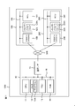
- FIG. 1 is a diagram illustrating an example of a hardware configuration of an information processing system according to the present embodiment.
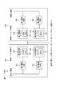
- FIG. 2 is a diagram showing the configuration of the control unit in the present embodiment.
- FIG. 3 is a diagram illustrating a power-on state during normal operation of the control unit in the present embodiment.
- FIG. 4 is a diagram for explaining a part of the internal configuration of the control unit in the present embodiment.
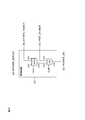
- FIG. 5 is a diagram for explaining a part of the internal configuration of the control circuit in this embodiment.
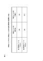
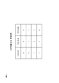
- FIG. 6 is a diagram for explaining a truth table of the exclusive OR circuit of the control circuit in this embodiment.
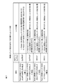
- FIG. 7 is a diagram for explaining the relationship between the GPIO signal of the control unit and the register value in this embodiment.
- FIG. 1 is a diagram illustrating an example of a hardware configuration of an information processing system according to the present embodiment.
- FIG. 2 is a diagram showing the configuration of the control unit in the present embodiment.
- FIG. 3 is a diagram illustrating a power-
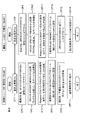
- FIG. 8 is a sequence diagram showing a startup process after the apparatus power of the control unit in this embodiment is turned on.
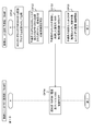
- FIG. 9 is a sequence diagram showing processing when a failure occurs in the control unit in the present embodiment.
- FIG. 10 is a sequence diagram illustrating processing when a failure occurs in the control unit according to this embodiment.
- FIG. 1 is a diagram illustrating an example of a hardware configuration of an information processing system in the present embodiment.
- the information processing system 1000 includes an information processing apparatus 10, a control unit 100, and a control unit 200.
- the information processing system 1000 includes a network 500 that connects the information processing apparatus 10 and the control unit 100 and connects the information processing apparatus 10 and the control unit 200.
- the control unit 100 and the control unit 200 have the same configuration.
- the same components as those described in the control unit 100 are denoted by the same reference numerals, and description thereof is omitted.
- the information processing apparatus 10 includes a CPU (Central Processing Unit) 11, a memory 12, a PSU (Power Supply Unit) 13, a fan unit 14, a communication interface 15, and a bus 16.
- the CPU 11, the memory 12, the PSU 13, the fan unit 14, and the communication interface 15 are connected to each other via a bus 16.
- the CPU 11 executes various processes of the information processing apparatus 10.
- the memory 12 temporarily stores at least a part of an OS (Operating System) program executed by the CPU 11, an application program, and a program for controlling the information processing apparatus 10.
- the memory 12 stores various data necessary for processing in the CPU 11.
- the program 12A may be held in a storage medium other than the memory 12.
- the program 12A is stored in a “portable physical storage medium” such as a flexible disk (FD), a CD-ROM, an MO disk, a DVD disk, a magneto-optical disk, and an IC card inserted into the information processing apparatus 10, for example.
- the program 12A is a disk device provided inside or outside the information processing apparatus 10, or “another computer (or connected to the information processing apparatus 10 via a LAN (Local Area Network), a network, a public line, the Internet, a WAN, etc. (or Server) ”is stored in a storage medium (not shown).
- the CPU 11 reads the program 12A from the memory 12 and executes the program 12A.
- the PSU 13 supplies a DC voltage to the CPU 11, the memory 12, the fan unit 14, and the communication interface 15 of the information processing apparatus 10.
- the fan unit 14 cools the CPU 11, the memory 12, the PSU 13, and the communication interface 15 of the information processing apparatus 10.
- the communication interface 15 is provided for the information processing apparatus 10 to connect to the control unit 100 and the control unit 200 via the network 500.
- the communication interface 15 provides an interface function for transmitting and receiving data between the CPU 11 and the memory 12.
- the control unit 100 includes an MCU (Microcontroller Unit) 141, a USB memory 123 as an example of a memory, a midplane connector 150, and a bus 160.
- the MCU 141, the USB memory 123, and the midplane connector 150 are connected to each other via a bus 160.
- the control unit 100 has the same configuration as the control unit 200, and can perform the same operation equivalent to each other.
- the control unit 100 has a function of detecting an internal failure that occurs in the control unit 100. The detection result of the internal failure is transmitted to the control unit 200 via the midplane connector 150 and the network 500.
- the control unit 200 is connected to the information processing apparatus 10 instead of the control unit 100, so that power control for the CPU 11, the memory 12, the PSU 13, the fan unit 14, and the communication interface 15 of the information processing apparatus 10 is performed. Initialization and monitoring can be performed.
- the MCU 141 executes various processes of the control unit 100.
- the MCU 141 performs power control, initialization, and monitoring for the CPU 11, the memory 12, the PSU 13, the fan unit 14, and the communication interface 15 of the information processing apparatus 10.
- the MCU 141 serving as the first control unit processes the software 123A stored in the USB memory 123 that is a non-volatile memory, and instructs to update any of the software 123A stored in the USB memory 123. If there is, the software 123A stored in the USB memory 123 and instructed to be updated is updated.
- the USB memory 123 stores at least a part of an OS program executed by the MCU 141, an application program, and software 123A for controlling the control unit 100.
- the USB memory 123 stores various data necessary for processing in the MCU 141.
- the USB memory 123 stores error log information of the CPU 11, the memory 12, the fan unit 14, and the communication interface 15 of the information processing apparatus 10.
- the USB memory 123 stores setting information including configuration information that can be arbitrarily set by the user of the information processing apparatus 10. Further, the USB memory 123 stores FRU (Field Replacement Unit) information in the CPU 11, the memory 12, the PSU 13, the fan unit 14, and the communication interface 15 of the information processing apparatus 10.
- the USB memory 123 stores various backup information in the CPU 11 and the memory 12 of the information processing apparatus 10.
- the USB 123 stores firmware that detects an error of the control unit 100. Further, the USB memory 123 stores a log in which the cause of failure of the control unit 100 and the control unit 200 is recorded.
- the USB memory 123 is duplicated with the USB memory 223 in order to ensure that data stored in the USB memory 123 is prevented from being damaged.
- the USB memory 123 stores the same data and program as the data stored in the USB memory 223 and the software 223A.
- the midplane connector 150 is provided for the control unit 100 to connect to the information processing apparatus 10 and the control unit 200 via the network 500.
- the midplane connector 150 transmits and receives data between the control unit 100 and the information processing apparatus 10 or between the control unit 100 and the control unit 200.
- the control unit 200 includes an MCU 241, a USB memory 223, and a midplane connector 250.
- the MCU 241, USB memory 223, and midplane connector 250 are connected to each other via a bus 260.
- the control unit 200 has the same configuration as the control unit 100, and can perform the same operation equivalent to each other.
- the control unit 200 has a function of detecting an internal failure that occurs in the own device. The detection result of the internal failure is transmitted to the control unit 100 via the midplane connector 250 and the network 500.
- the control unit 100 connects to the information processing apparatus 10 instead of the control unit 200, so that power control for the CPU 11, the memory 12, the PSU 13, the fan unit 14, and the communication interface 15 of the information processing apparatus 10 is performed. Initialization and monitoring can be performed.
- the MCU 241 as the second control unit when the abnormality of the control unit 100 as the active processing device is detected by the CPLD as the detection unit, the USB memory 223 as the non-volatile memory when the MCU 241 is activated.
- the software 223A stored in is processed.
- the USB memory 223 is duplicated with the USB memory 123 in order to ensure that data stored in the USB memory 223 is prevented from being damaged.
- the USB memory 223 stores the same data and program as the data stored in the USB memory 123 and the software 123A. That is, the information processing system 1000 includes nonvolatile memories 123 and 223 that store software 123A and 223A, an active processing device 100, and a standby processing device 200.
- FIG. 2 is a diagram showing the configuration of the control unit 100 and the control unit 200 in the present embodiment.
- the same components as those described with reference to FIG. 2 are identical with reference to FIG. 1 and the same components as those described with reference to FIG. 2;
- the control unit 100 includes a first power supply circuit 110, a first power supply system device 120, a second power supply circuit 130, and a second power supply system device 140.
- the control unit 100 includes a first power supply circuit 110 and a second power supply circuit 130 that are separated into two systems. In the example of FIG. 2, the control unit 100 operates as an active system.
- the first power supply circuit 110 is connected to the apparatus main power supply.
- the first power supply circuit 110 supplies a DC voltage to the first power supply system device 120.
- the first power supply circuit 110 supplies a DC voltage to the first power supply system device 120 when the control unit 100 operates as an active system.
- the first power supply system device 120 is supplied with a DC voltage by the first power supply circuit 110.
- the first power supply system device 120 includes, for example, a USB memory 123.
- the first power supply system device 120 is always powered on by the first power supply circuit 110 in order to multiplex data with the USB memory 223 of the control unit 200.
- the first power supply device 120 is powered on by the first power supply circuit 110 regardless of the active / standby system.
- the second power supply circuit 130 is connected to the apparatus main power supply in the same manner as the first power supply circuit 110.
- the second power supply circuit 130 is a circuit that supplies a DC voltage to the second power supply system device 140.
- the second power supply circuit 130 supplies a DC voltage to the second power supply system device 140 when the control unit 100 operates as an active system. When the control unit 100 operates as a standby system, the second power supply circuit 130 is not turned on.
- the second power supply system device 140 is supplied with a DC voltage by the second power supply circuit 130.
- the second power supply system device 140 includes, for example, an MCU 141.
- the second power supply system device 140 is connected to other control units 200 to monitor and control the CPU 11, the memory 12, the PSU 13, the fan unit 14, and the communication interface 15 that are control target units of the information processing apparatus 10. Includes devices used to communicate.
- the second power supply system device 140 is powered on when the control unit 100 operates as an active system.
- the control unit 200 includes a first power supply circuit 210, a first power supply system device 220, a second power supply circuit 230, and a second power supply system device 240. Similar to the control unit 100, the control unit 200 includes a first power supply circuit 210 and a second power supply circuit 230 that are separated into two systems. The control unit 200 operates as a standby system in the example of FIG.
- the first power supply circuit 210 is connected to the apparatus main power supply.
- the first power supply circuit 210 supplies a DC voltage to the first power supply system device 220.
- the first power supply circuit 210 supplies a DC voltage to the first power supply system device 220 even when the control unit 200 operates as a standby system.
- the first power supply device 220 is supplied with a DC voltage by the first power supply circuit 210.
- the first power supply system device 220 includes, for example, a USB memory 223. Since the first power supply system device 220 multiplexes data with the USB memory 123 of the control unit 100, the first power supply circuit 210 is always powered on even when the control unit 200 operates as a standby system.
- the second power supply circuit 230 is connected to the apparatus main power supply in the same manner as the first power supply circuit 210.
- the second power supply circuit 230 is a circuit that supplies a DC voltage to the second power supply system device 240.
- the second power supply circuit 230 does not supply a DC voltage to the second power supply system device 240 when the control unit 200 operates as a standby system.
- the second power supply system device 240 is supplied with a DC voltage by the second power supply circuit 230.
- the second power supply system device 240 includes, for example, an MCU 241.
- the second power supply system device 240 is connected to other control units 100 in order to monitor and control the CPU 11, the memory 12, the PSU 13, the fan unit 14, and the communication interface 15 that are control target units of the information processing apparatus 10. Includes devices used to communicate.
- the second power supply system device 240 is not turned on when the control unit 200 operates as a standby system.
- FIG. 3 is a diagram illustrating a power-on state during normal operation of the control unit 100 and the control unit 200 in the present embodiment.
- the normal operation indicates a case where the control unit 100 operates as an active system and the control unit 200 operates as a standby system.
- the same components as those described in FIGS. 1 and 2 are denoted by the same reference numerals, and description thereof is omitted.
- the control unit 100 when the control unit 100 operates as the active system, the first power supply system device 120 and the second power supply system device 140 are powered on.
- the control unit 200 when the control unit 200 operates as a standby system, the first power system device 220 is powered on and the second power system device 240 is not powered. That is, when the control unit 200 operates as a standby system, power is not turned on except for devices necessary for data synchronization with the control unit 100 operating as an active system.
- FIG. 4 is a diagram for explaining a part of the internal configuration of the control unit 100 and the control unit 200 in this embodiment.
- the same components as those described in FIGS. 1 to 3 are denoted by the same reference numerals, and description thereof is omitted.
- the control unit 100 includes a first power supply circuit 110, a control circuit 121, a GPIO (General Purpose Input Output: general purpose input / output) 122, a USB (Universal Serial Bus) memory 123, a USB switch 124, a second power supply circuit 130, an MCU 141, and BOOT. It has an FMEM (Flash Memory) 143, a CPLD (Configurable Programmable Logic Device) 144, a peripheral device 145, and a midplane connector 150. In FIG. 4, the control unit 100 operates as an active system.
- the first power supply system device 120 described above with reference to FIG. 2 includes a control circuit 121, a GPIO 122, a USB memory 123, and a USB switch 124. As described above with reference to FIG. 2, the first power supply system device 120 is supplied with a DC voltage by the first power supply circuit 110. 2 includes the MCU 141, the BOOT FMEM 143, the CPLD 144, and the peripheral device 145. As described above with reference to FIG. 2, the second power supply system device 140 is supplied with a DC voltage by the second power supply circuit 130.
- the control circuit 121 is connected to the GPIO 122 of the control unit 100, the second power supply circuit 130, the control circuit 221, the GPIO 222, and the CPLD 244 of the control unit 200 through a bus.
- the control circuit 121 instructs the second power supply circuit 130 to turn on and off the power based on the instructions from the GPIO 122, the GPIO 222, and the CPLD 244 via the bus.
- the GPIO 122 is connected to the MCU 141 by I2C (Inter-Integrated Circuit).
- the GPIO 122 sets Port 0, Port 1, Port 2, and Port 3 based on an instruction from the MCU 141 via I2C.
- the GPIO 122 has a built-in register for storing the settings of Port 0, Port 1, Port 2, and Port 3.
- Port 0 of the GPIO 122 is connected to the control circuit 121 by a bus.
- Port 1 of GPIO 122 is connected to Port 2 of GPIO 222 of control unit 200 by a bus.
- Port 2 of the GPIO 122 is connected to Port 1 of the GPIO 222 of the control unit 200 via the midplane connector 150 and the midplane connector 250 by a bus.
- Port 3 of the GPIO 122 is connected to the CPLD 244 of the control unit 200 via the midplane connector 150 and the midplane connector 250 by a bus.
- the USB memory 123 is connected to the USB switch 124 by USB 2.0.
- the USB memory 123 transmits and receives stored data to and from the USB switch 124 via USB 2.0.
- the USB switch 124 is connected to the CPLD 244 of the control unit 200 through the midplane connector 150 and the midplane connector 250 by Port Assign Interface.
- Port Assign Interface is an input signal for setting Port 0 or Port 1 of the USB switch 124.
- the USB switch 124 is connected to the MCU 141 by I2C.
- Port 0 of the USB switch 124 is connected to the MCU 141 by USB 2.0.
- Port 1 of the USB switch 124 is connected to the MCU 241 of the control unit 200 by the USB 2.0 via the midplane connector 150 and the midplane connector 250.
- the MCU 141 is connected to the midplane connector 150 by a bus.
- the MCU 141 is connected to Port 0 of the USB switch 124 by USB 2.0.
- the MCU 141 is connected to Port 1 of the USB switch 224 of the control unit 200 via the midplane connector 150 and the midplane connector 250 by USB 2.0.
- the MCU 141 is connected to the BOOT FMEM 143 and the CPLD 144 by a bus.
- the MCU 141 has a built-in GPIO.
- the BOOT FMEM 143 is connected to the MCU 141 via a bus.
- the BOOT FMEM 143 stores a startup program for the MCU 141.
- the boot program stored in the BOOT FMEM 143 incorporates a program for initializing the peripheral device 145.
- the boot program stored in the BOOT FMEM 143 includes a process of reading the setting information of Port 0, Port 1, Port 2, and Port 3 stored in the register of the GPIO 122 by the MCU 141 and confirming what the MCU 141 activation factor is. Note that the process after the MCU 141 is activated is changed depending on the cause of the MCU 141 activation.
- CPLD 144 is connected to MCU 141 by a bus.
- the CPLD 144 is connected to the USB switch 224 of the control unit 200 through the midassign connector 150 and the midplane connector 250 by Port Assign Interface.
- the CPLD 144 is connected to the Port 3 of the GPIO 222 of the control unit 200 via the midplane connector 150 and the midplane connector 250 by a bus.
- the CPLD 144 incorporates a watchdog timer that is a circuit for monitoring the operation status of the MCU 141.
- the CPLD 144 determines that an operation error has occurred in the MCU 141 when there is no response from the MCU 141 for a predetermined time or more when the MCU 141 is activated or in operation.
- the CPLD 144 After determining that an operation abnormality has occurred in the MCU 141, the CPLD 144 asserts an MCU 141 reset signal or an interrupt (NMI-maskable interrupt: NMI) signal to the USB switch 224 and the Port 3 of the GPIO 222. That is, the CPLD 144 detects the occurrence of an abnormality in the MCU 141 that is the first control unit.
- NMI NMI-maskable interrupt
- Peripheral devices 145 include NIC (Network Interface Card), Hub (concentrator), I2C Controller, DRAM (Dynamic Random Access Memory, MRAM (Magnetorism EDM), MRAM (Magnetic Resistive Random Memory LED). Includes Erasable Programmable Read Only Memory).
- the peripheral device 145 is a device used for managing and controlling the information processing apparatus 10.
- the midplane connector 150 is a connector for connecting the control unit 100 to the information processing apparatus 10 and the control unit 200.
- the midplane connector 150 receives a signal corresponding to the slot position from the slot # 0 of the information processing system 1000.
- the midplane connector 150 transmits to the MCU 141 an identification signal for identifying whether the control unit 100 is an active system or a standby system to the connected control unit 100.
- the MCU 141 When the power is turned on by the second power supply circuit 130, the MCU 141 reads the MCU 141 activation program stored in the BOOT FMEM 143 and activates the MCU 141.
- the MCU 141 executes a program for initializing the peripheral device 145 stored in the BOOT FMEM 143 when the MCU 141 is activated, and initializes the peripheral device 145.
- the MCU 141 executes processing for reading out the setting information of Port 0, Port 1, Port 2, and Port 3 stored in the register of the GPIO 122 among the programs stored in the BOOT FMEM 143 by the MCU 141.
- the MCU 141 confirms what is the activation factor of the MCU 141 from the setting information of Port 0, Port 1, Port 2, and Port 3 stored in the register of the GPIO 122. Based on the identification signal input from the midplane connector 150, the MCU 141 recognizes whether the control unit 100 is an active system or a standby system.
- the MCU 141 may become uncontrollable, and the watchdog timer of the CPLD 144 may time out without detecting a heartbeat from the MCU 141.
- the CPLD 144 switches from the connection of the MCU 141 by the Port 1 of the USB switch 224 to the connection by the MCU 241 by the Port 0 via the Port Assign Interface.
- the MCU 241 can be connected to the USB memory 223 via the USB switch 224.
- the control unit 200 includes a first power circuit 210, a control circuit 221, a GPIO 222, a USB memory 223, a USB switch 224, a second power circuit 230, an MCU 241, a BOOT FMEM 243, a CPLD 244, a peripheral device 245, and a midplane connector 250. Note that the control unit 200 operates as a standby system. In the control unit 200, the same components as those described in the control unit 100 are denoted by the same reference numerals, and the description thereof is omitted.
- the first power supply system device 220 described above with reference to FIG. 2 includes a control circuit 221, a GPIO 222, a USB memory 223, and a USB switch 224.
- the first power supply device 220 is supplied with a DC voltage by the first power supply circuit 210 as described above with reference to FIG. 2 includes the MCU 241, the BOOT FMEM 243, the CPLD 244, and the peripheral device 245.
- the second power supply system 240 is supplied with a DC voltage by the second power supply circuit 230.
- the control circuit 221 is connected to the GPIO 222 of the control unit 200, the second power supply circuit 230, the GPIO 122 of the control unit 100, and the CPLD 144 via a bus.
- the control circuit 221 instructs the second power supply circuit 230 to turn on and off based on instructions from the GPIO 222, the GPIO 122, and the CPLD 144 via the bus. That is, the control circuit 221 that is a start control unit outputs a start instruction to the MCU 241 that is a second control unit.
- the GPIO 222 is connected to the MCU 241 by I2C.
- the GPIO 222 sets Port 0, Port 1, Port 2, and Port 3 based on an instruction from the MCU 241 via the I2C.
- the GPIO 222 has a built-in register for storing the settings of Port 0, Port 1, Port 2, and Port 3.
- Port 0 of the GPIO 222 is connected to the control circuit 221 by a bus.
- Port 1 of the GPIO 222 is connected to the control circuit 121 and the Port 2 of the GPIO 122 via the midplane connector 150 and the midplane connector 250 by a bus.
- Port 2 of GPIO 222 is connected to Port 1 of GPIO 122 via a midplane connector 150 and a midplane connector 250 by a bus.
- Port 3 of the GPIO 222 is connected to the CPLD 144 by a bus via the midplane connector 150 and the midplane connector 250.
- the USB memory 223 is connected to the USB switch 224 by USB 2.0.
- the USB memory 223 transmits and receives data stored in the USB memory 223 with the USB switch 224 via the USB 2.0.
- the USB switch 224 is connected to the CPLD 144 of the control unit 100 through the midplane connector 150 and the midplane connector 250 by Port Assign Interface.
- Port Assign Interface is an input signal for setting Port 0 or Port 1 of the USB switch 224.
- the USB switch 224 is connected to the MCU 241 through I2C.
- Port 0 of the USB switch 224 is connected to the MCU 241 via USB 2.0.
- Port 1 of the USB switch 224 is connected to the MCU 141 via the USB 2.0 via the midplane connector 150 and the midplane connector 250.
- the MCU 241 is connected to the midplane connector 250 by a bus.
- the MCU 241 is connected to Port 0 of the USB switch 224 by USB 2.0.
- the MCU 241 is connected to Port 1 of the USB switch 124 via the midplane connector 150 and the midplane connector 250 by USB 2.0.
- the MCU 241 is connected to the BOOT FMEM 243 and the CPLD 244 by a bus.
- the MCU 241 has a built-in GPIO.
- the BOOT FMEM 243 is connected to the MCU 241 via a bus.
- the BOOT FMEM 243 stores an activation program for the MCU 241.
- the boot program stored in the BOOT FMEM 243 incorporates a program for initializing the peripheral device 245.
- the boot program stored in the BOOT FMEM 243 includes processing for reading out the setting information of Port 0, Port 1, Port 2, and Port 3 stored in the register of the GPIO 222 by the MCU 241 and confirming what is the cause of the MCU 241. Note that the processing after the MCU 241 is activated is changed depending on what is the activation factor of the MCU 241.
- CPLD 244 is connected to MCU 241 by a bus.
- the CPLD 244 is connected to the USB switch 124 via the midplane connector 150 and the midplane connector 250 by the Port Assign Interface.
- the CPLD 244 is connected to the Port 3 of the GPIO 122 via the midplane connector 150 and the midplane connector 250 by a bus.
- the CPLD 244 has a built-in watchdog timer that is a circuit for monitoring the operation status of the MCU 241.
- the CPLD 244 determines that an operation abnormality has occurred in the MCU 241 when there is no response from the MCU 241 for a predetermined time or more when the MCU 241 is activated or in operation. After determining that an abnormal operation has occurred in the MCU 241, the CPLD 244 asserts a reset signal or interrupt (NMI) signal of the MCU 241 to the USB switch 124 and Port 3 of the GPIO 222.
- NMI reset signal or interrupt
- Peripheral devices 245 include NIC, Hub, I2C Controller, DRAM, MRAM, Sensor, LED controller, and E2PROM.
- the peripheral device 245 is a device used for managing and controlling the information processing apparatus 10, similarly to the peripheral device 145 of the control unit 100.
- the midplane connector 250 is a connector that connects the control unit 200 to the information processing apparatus 10 and the control unit 100.
- a signal corresponding to the slot position is input from Slot # 1 of the information processing system 1000.
- the midplane connector 250 transmits, to the MCU 241, an identification signal for identifying whether the control unit 200 is an active system or a standby system to the connected control unit 200.
- the MCU 241 When the power is turned on by the second power supply circuit 230, the MCU 241 reads the MCU 241 activation program stored in the BOOT FMEM 243 and activates the MCU 241. The MCU 241 executes a program for initializing the peripheral device 245 stored in the BOOT FMEM 243 when the MCU 241 is activated, and initializes the peripheral device 245. The MCU 241 executes a process of reading out setting information of Port 0, Port 1, Port 2, and Port 3 stored in the register of the GPIO 222 among the programs stored in the BOOT FMEM 243 by the MCU 241 when the MCU 241 is activated.
- the MCU 241 confirms what is the activation factor of the MCU 241 from the setting information of Port 0, Port 1, Port 2, and Port 3 stored in the GPIO 222 register. The MCU 241 recognizes whether the control unit 100 is the active system or the standby system based on the identification signal input from the midplane connector 250.
- the MCU 241 may become uncontrollable, and the watchdog timer of the CPLD 244 may time out without being able to detect the heartbeat from the MCU 241.
- the CPLD 244 is connected to the Port 1 of the USB switch 124 via the Port Assign Interface.
- the MCU 241 is switched from the connection by the MCU 241 to the connection by the MCU 141 by Port 1.
- Port 0 of the USB switch 124 By connecting Port 0 of the USB switch 124 to the MCU 141, the MCU 141 can be connected to the USB memory 123 via the USB switch 124.
- FIG. 5 is a diagram for explaining the internal configuration of the control circuit 121 in this embodiment.
- the same components as those described in FIGS. 1 to 4 are denoted by the same reference numerals, and description thereof is omitted.
- control circuit 121 includes an exclusive OR circuit 121A and an OR circuit 121B.
- the exclusive OR circuit 121A has a terminal X1, a terminal X2, and a terminal X3.
- the terminal X1 is connected to Port 0 of the GPIO 122.
- the terminal X2 is connected to Port 2 of the GPIO 122 and Port 1 of the GPIO 222 of the control unit 200.
- the terminal X3 is connected to the terminal Y1 of the OR circuit 121B.
- the OR circuit 121B has a terminal Y1, a terminal Y2, and a terminal Y3.
- the terminal Y1 is connected to the terminal X3 of the exclusive OR circuit 121A.
- the terminal Y2 is connected to the Port 3 of the GPIO 122 and the CPLD 244 of the control unit 200.
- the terminal Y3 is connected to the second power supply circuit 130.
- the POWER_ENABLE signal is input from the Port 0 of the GPIO 122 to the terminal X1.
- the POWER_ENABLE signal is a signal output for asserting a valid signal of the second power supply circuit 130 of the control unit 100. The assertion of a signal means that the signal is set to a high level.
- the OTHER_ENABLE signal is input from the GPIO 222 of the control unit 200 to the terminal X2.
- the OTHER_ENABLE signal is a signal output from the control unit 200 to turn on the second power supply circuit 130 of the control unit 100 when an error occurs in the control unit 200.
- the terminal Y2 receives a WDT_ENABLE signal from the CPLD 244 of the control unit 200.
- the WDT_ENABLE signal is a signal output to turn on the power of the second power supply circuit 130 of the control unit 100 from the watchdog timer built in the CPLD 244 of the control unit 200.
- the terminal Y3 outputs a POWER_ON signal to the second power supply circuit 130 of the control unit 100.
- the POWER_ON signal is a signal output to turn on the power supply of the second power supply circuit 130 of the control unit 100.
- FIG. 6 is a diagram for explaining a truth table of the exclusive OR circuit 121A of the control circuit 121 in this embodiment.
- the truth table in FIG. 6 is a table in which all input / output relationships of the exclusive OR circuit 121A are represented by truth values.
- FIG. 7 is a diagram for explaining the relationship between the signal of the GPIO 122 of the control unit 100 and the register value stored in the GPIO 122 in this embodiment.
- the GPIO 122 changes the settings of Port 0, Port 1, Port 2, and Port 3 built in the GPIO 122 based on an instruction from the MCU 141.
- a signal output from Port 0 of the GPIO 122 corresponds to a POWER_ENABLE signal output to the control circuit 121.
- a signal for turning on the power of second power supply circuit 130 of control unit 100 is output from Port 0 of GPIO 122.
- a signal for turning off the power of the second power supply circuit 130 of the control unit 100 is output from the Port 0 of the GPIO 122.
- the signal output from Port 1 of GPIO 122 corresponds to the OTHER_ENABLE signal output to the control circuit 221 of the control unit 200.
- a Normal signal indicating a normal state without an error is output from the Port 1 of the GPIO 122 to the control circuit 221 of the control unit 200.
- the register value of Port 1 of the GPIO 122 is set to “1”
- an error has occurred in the control unit 100, so that an Error signal indicating that the power supply of the second power supply circuit 130 of the control unit 200 is turned on is displayed on the GPIO 122. It is output from Port 1 to the control circuit 221 of the control unit 200.
- the signal input to Port 2 of GPIO 122 corresponds to the OTHER_ENABLE signal input from Port 1 of GPIO 222 of control unit 200.
- the register value of Port 2 of GPIO 122 is set to “0”, it indicates that a Normal signal indicating a normal state without error is input from Port 1 of GPIO 222 to Port 2 of GPIO 122.
- the register value of Port 2 of the GPIO 122 is set to “1”
- an error has occurred in the control unit 100 when the control unit 200 operates as an active system, so that the power supply of the second power supply circuit 130 of the control unit 100 is An Error signal indicating that the switch is turned on indicates that Port 1 of the GPIO 222 is input to Port 2 of the GPIO 122.
- a signal input to Port 3 of GPIO 122 corresponds to a WDT_ENABLE signal input from CDLD 244 of control unit 200.
- the register value of Port 3 of GPIO 122 is set to “0”, it indicates that a Normal signal indicating a normal state without error has been input to Port 3 of GPIO 122 from CDLD 244 of control unit 200.
- the register value of Port 3 of the GPIO 122 is set to “1”, an error has occurred in the control unit 200 when the control unit 200 operates as an active system, so the power supply of the second power supply circuit 130 of the control unit 100 is An error signal indicating that the signal is turned on is input from the CDLD 244 of the control unit 200 to the Port 3 of the GPIO 122.
- FIG. 8 is a sequence diagram showing processing during normal operation of the control unit 100 and the control unit 200 in the present embodiment.
- the same components as those described in FIGS. 1 to 7 are denoted by the same reference numerals, and the description thereof is omitted.
- the control unit 100 operates as an active system.
- the control unit 200 operates as a standby system.
- the first power supply circuit 110 of the control unit 100 when the main power supply of the control unit 100 is turned on (OP1), the first power supply circuit 110 of the control unit 100 is turned on (OP2).
- the first power supply circuit 110 powers on the first power supply system device 120.
- “High” (1) is asserted to the POWER_ENABLE signal output from Port 0 of the GPIO 122 (OP2).
- power is turned on to the second power supply circuit 130 of the control unit 100 (OP2).
- the second power supply circuit 130 turns on the second power supply system device 140.
- the register values of GPIO 122 are POWER_ENABLE: 1, OTHER_ENABLE: 0, WDT_ENABLE: 0, and POWER_ON: 1.
- the MCU 141 of the control unit 100 reads the activation program stored in the BOOT FMEM 143 (OP3).
- the MCU 141 initializes the peripheral device 145 (OP3).
- the MCU 141 recognizes that the control unit 100 is the active system based on the Slot # 0 identification signal input from the midplane connector 150 (OP4).
- the MCU 141 sets the port setting on the upstream side of the USB switch 124 of the control unit 100 to Port 0 (OP5). That is, the MCU 141 sets the port setting on the side from the USB switch 124 to the MCU 141 to Port 0 (OP5).
- the MCU 141 starts dual writing of data and programs to the USB memory 123 of the control unit 100 and the USB memory 223 of the control unit 200 (OP6).
- the control unit 100 shifts to a normal operation business (OP7).
- the normal operation business indicates an operation business in which the control unit 100 operates as an active system and the control unit 200 operates as a standby system.
- the control unit 200 When the apparatus main power is turned on (OP8), the control unit 200 is turned on to the first power supply circuit 210 of the control unit 200 (OP9).
- the first power supply circuit 210 powers on the first power supply system device 220.
- “High” (1) is asserted to the POWER_ENABLE signal output from Port 0 of the GPIO 222 (OP9).
- power is turned on to the second power supply circuit 230 of the control unit 200 (OP9).
- the second power supply circuit 230 powers on the second power supply system device 240.
- the MCU 241 of the control unit 200 reads the activation program stored in the BOOT FMEM 243 and activates it (OP10).
- the MCU 241 initializes the peripheral device 245 (OP10).
- the MCU 241 recognizes that the control unit 200 is a standby system based on the Slot # 1 identification signal input from the midplane connector 250 (OP11).
- the MCU 241 sets the port setting on the upstream side of the USB switch 224 of the control unit 200 to Port 1 (OP12). That is, the MCU 241 sets the port setting on the side from the USB switch 224 to the MCU 241 to Port 1 (OP12).
- the MCU 241 controls the GPIO 222 via the I2C, and asserts “Low” (0) to the POWER_EN signal output from the Port 0 of the GPIO 222 (OP13).
- the register values of GPIO 222 are POWER_ENABLE: 0, OTHER_ENABLE: 0, WDT_ENABLE: 0, and POWER_ON: 0.
- FIGS. 9 to 10 are sequence diagrams showing processing when a failure occurs in the control unit 100 in this embodiment.
- the processing shown in A of FIG. 9 continues to A of FIG. 9 to 10, the same reference numerals are given to the same components as those described in FIGS. 1 to 8, and the description thereof will be omitted.
- the control unit 100 operates as an active system.
- the control unit 200 operates as a standby system.
- the CPLD 144 determines whether the MCU 141 has become uncontrollable using the watchdog timer built in the CPLD 144 ( OP22). Specifically, the CPLD 144 determines that an operation abnormality has occurred in the MCU 141 when there is no response from the MCU 141 for a predetermined time or more when the MCU 141 is activated or in operation.
- the MCU 141 When the MCU 141 has not become uncontrollable (OP22 N), the MCU 141 reads the firmware stored in the USB memory 123 and detects an error of the control unit 100 (OP23).
- the CPLD 144 of the control unit 100 turns on the power of the second power supply circuit 230 of the control unit 200 (OP27). Specifically, as a process after an abnormal operation occurs in the MCU 141 and the watchdog timer of the CPLD 144 cannot detect a heartbeat from the MCU 141 and times out, a signal for the CPLD 144 to turn on the power of the control unit 200 ( WDT_ENABLE) is asserted. Since the MCU 141 cannot be controlled, the power supply to the second power supply circuit 230 and the second power supply system device 240 of the control unit 200 is performed by the CPLD 144.
- the process of turning on the power to the second power supply circuit 230 and the second power supply system 240 of the control unit 200 when the MCU 141 has become uncontrollable (OP22 Y) will be described.
- the CPLD 144 asserts “High” (1) to the WDT_ENABLE signal output to the control circuit 221 of the control unit 200.
- “High” (1) is asserted in the POWER_ON signal output from the control circuit 221 to the second power supply circuit 230. Therefore, power is turned on to the second power supply circuit 230 of the control unit 200.
- the register values of GPIO 222 are POWER_ENABLE: 0, OTHER_ENABLE: 0, WDT_ENABLE: 1 and POWER_ON: 1.
- the MCU 141 detects the error of the control unit 100 (OP23), and then reads the firmware stored in the USB memory 123 to identify the faulty part of the control unit 100 (OP24). Next, the MCU 141 records the specified failure location of the control unit 100 in the USB memory 123 and the USB memory 223 that is duplicated with the USB memory 123 (OP24). Next, the MCU 141 controls the GPIO 122 of the control unit 100 to turn on the power of the second power system device 240 of the control unit 200 (OP25). Specifically, “High” (1) is asserted to the OTHER_ENABLE signal output from the Port 1 of the GPIO 122 to the control circuit 221 of the control unit 200. Next, the second power supply circuit 230 of the control unit 200 is turned on (OP25). The register values of GPIO 122 are POWER_ENABLE: 0, OTHER_ENABLE: 1, WDT_ENABLE: 0, and POWER_ON: 1.
- the MCU 141 accesses the USB switch 224 of the control unit 200 via the Port Assign Interface and changes the setting of the USB switch 224 (OP26). After changing the setting of the USB switch 224, the MCU 241 of the control unit 200 can access the USB memory 223 (OP26). Specifically, the MCU 141 sets Port 1 of the USB switch 224 to Port 0.
- the CPLD 144 turns on the power supply of the second power supply circuit 230 of the control unit 200 (OP27).
- the CPLD 144 accesses the USB switch 224 of the control unit 200 via the Port Assign Interface and changes the setting of the USB switch 224 (OP28). That is, the CPLD 144 detects an abnormality of the MCU 141 serving as the first control unit, accesses the USB switch 224, and changes the setting of the USB switch 224.
- the MCU 241 of the control unit 200 can access the USB memory 223 (OP28). Specifically, the CPLD 144 sets Port 1 of the USB switch 224 to Port 0.
- the MCU 241 of the control unit 200 reads and starts the startup program stored in the BOOT FMEM 243 (OP31).
- the MCU 241 reads the register values of the GPIO 222, Port 0, Port 1, Port 2, and Port 3, and confirms the activation factor of the MCU 241.
- the MCU 241 is activated when the MCU 141 has become uncontrollable (OP22 Y)
- the MCU 241 reads and activates the activation program (OP31), it reads Port 0, Port 1, Port 2, and Port 3 of the register of the GPIO 222, and confirms the activation factor of the MCU 141.
- “High” (1) is asserted to WDT_ENABLE output from the CPLD 144 to the GPIO 222. Therefore, “High” (1) is set in Port 3 of the register of the GPIO 222.
- “Low” (0) is set in Port 0, Port 1 and Port 2 of the GPIO 222 register.
- the MCU 241 controls the GPIO 222 via the I2C, and sends a POWER_ENABLE signal from the control circuit 221 to the second power supply circuit 230. Assert. Even if the WDT_ENABLE signal from the CPLD 144 is negated by asserting the POWER_ENABLE signal, the power supply of the second power supply circuit 230 is not cut off. For this reason, the power supply of the second power supply circuit 230 is maintained in the ON state. Since the power supply of the second power supply circuit 230 is maintained in the ON state, power can be supplied to the second power supply system device 240. Signal negation refers to invalidating a signal.
- the MCU 241 reads and starts the startup program stored in the BOOT FMEM 243 (OP31), and then reads a log recording the register value of the GPIO 222 and the failure factor of the control unit 100 recorded in the USB memory 223 (OP32). .
- the MCU 241 specifies the failure factor of the control unit 100 from the log in which the failure factor of the control unit 100 is recorded (OP32).
- the MCU 241 controls the GPIO 222 of the control unit 200 and turns off the power supply of the second power supply circuit 130 of the failed control unit 100 (OP33). That is, the MCU 241 that is the second control unit outputs the activation instruction to the MCU 241 and then the control unit 121 that is the activation control unit of the control unit 100 that is the active processing apparatus, the MCU 241 An instruction to disconnect the second power supply circuit 130 which is a power supply is output. Specifically, the MCU 241 asserts “High” (1) of the OTHER_ENABLE signal output from the Port 1 of the GPIO 222 to the Port 2 of the GPIO 122 of the control unit 100 via the I2C.
- the standby control unit 200 After the power of the second power supply circuit 130 of the failed control unit 100 is turned off, the standby control unit 200 becomes the active system.
- the control unit 200 that has become the active system starts monitoring and controlling the CPU 11, the memory 12, the PSU 13, the fan unit 14, and the communication interface 15 of the information processing apparatus 10 that is the control target unit group (OP35).
- the power supply of the second power supply system device 240 of the control unit 200 is cut off, so that the power consumption of the control unit 200 that is a standby system can be reduced.
- the power consumption can be reduced by about 90% as compared with the control unit 100 of the current system.
- the second power supply circuit 230 that is the power source of the MCU 241 that is the standby control unit is set in accordance with an activation instruction from the outside. throw into. Therefore, it is possible to maintain the consistency of the software 123A used in the current system without always turning on the second power supply circuit 230 that is a standby power supply. Therefore, power saving of the entire information processing system 1000 can be achieved.
- Information processing apparatus 11 CPU 12 memory 13 PSU 14 fan unit 15 communication interface 16 bus 100, 200 control unit 110, 210 first power supply circuit 120, 220 first power supply system device 121, 221 control circuit 121A exclusive OR circuit 121B OR circuit 122, 222 GPIO 123, 223 USB memory 124, 224 USB switch 130, 230 Second power supply circuit 140, 240 Second power supply system device 141, 241 MCU 143, 243 BOOT FMEM 144, 244 CPLD 145, 245 Peripheral device 150, 250 Midplane connector 160, 260 Bus 500 Network 1000 Information processing system
Landscapes
- Engineering & Computer Science (AREA)
- Theoretical Computer Science (AREA)
- Physics & Mathematics (AREA)
- General Engineering & Computer Science (AREA)
- General Physics & Mathematics (AREA)
- Quality & Reliability (AREA)
- Power Sources (AREA)
- Hardware Redundancy (AREA)
Abstract
[Problème] Produire un système de traitement d'informations et un procédé de traitement de système de traitement d'informations tels qu'il soit possible d'obtenir une consommation d'énergie réduite du système de traitement d'informations dans son ensemble. [Solution] Un système de traitement d'informations comprend un dispositif de traitement du courant, comprenant en outre une première mémoire non volatile qui contient un premier logiciel, et un dispositif de traitement de veille qui est connecté au dispositif de traitement du courant, comprenant en outre une seconde mémoire non volatile qui contient un second logiciel qui est synchronisé avec le premier logiciel. Le dispositif de traitement du courant comprend en outre une première unité de commande qui traite le premier logiciel qui est contenu dans la première mémoire non volatile, et si une instruction est émise pour actualiser le premier logiciel qui est contenu dans la première mémoire non volatile, effectue l'actualisation du logiciel qui est contenu dans la première mémoire non volatile.
Priority Applications (3)
| Application Number | Priority Date | Filing Date | Title |
|---|---|---|---|
| PCT/JP2011/001843 WO2012131761A1 (fr) | 2011-03-28 | 2011-03-28 | Système de traitement d'informations et procédé de traitement du système de traitement d'informations |
| JP2013506822A JP5682703B2 (ja) | 2011-03-28 | 2011-03-28 | 情報処理システム及び情報処理システムの処理方法 |
| US14/035,282 US9547567B2 (en) | 2011-03-28 | 2013-09-24 | Information processing system and processing method for information processing system |
Applications Claiming Priority (1)
| Application Number | Priority Date | Filing Date | Title |
|---|---|---|---|
| PCT/JP2011/001843 WO2012131761A1 (fr) | 2011-03-28 | 2011-03-28 | Système de traitement d'informations et procédé de traitement du système de traitement d'informations |
Related Child Applications (1)
| Application Number | Title | Priority Date | Filing Date |
|---|---|---|---|
| US14/035,282 Continuation US9547567B2 (en) | 2011-03-28 | 2013-09-24 | Information processing system and processing method for information processing system |
Publications (1)
| Publication Number | Publication Date |
|---|---|
| WO2012131761A1 true WO2012131761A1 (fr) | 2012-10-04 |
Family
ID=46929613
Family Applications (1)
| Application Number | Title | Priority Date | Filing Date |
|---|---|---|---|
| PCT/JP2011/001843 Ceased WO2012131761A1 (fr) | 2011-03-28 | 2011-03-28 | Système de traitement d'informations et procédé de traitement du système de traitement d'informations |
Country Status (3)
| Country | Link |
|---|---|
| US (1) | US9547567B2 (fr) |
| JP (1) | JP5682703B2 (fr) |
| WO (1) | WO2012131761A1 (fr) |
Cited By (1)
| Publication number | Priority date | Publication date | Assignee | Title |
|---|---|---|---|---|
| CN110554879A (zh) * | 2019-07-26 | 2019-12-10 | 深圳震有科技股份有限公司 | 一种基于处理器的烧录方法、系统和计算机设备 |
Families Citing this family (5)
| Publication number | Priority date | Publication date | Assignee | Title |
|---|---|---|---|---|
| CN105912488B (zh) * | 2016-05-20 | 2019-02-05 | 英业达科技有限公司 | 计算机装置及其控制方法 |
| CN110618909B (zh) * | 2019-09-27 | 2021-03-26 | 苏州浪潮智能科技有限公司 | 基于i2c通讯的故障定位方法、装置、设备及存储介质 |
| CN111767242B (zh) * | 2020-05-28 | 2022-04-15 | 西安广和通无线软件有限公司 | Pcie设备控制方法、装置、计算机设备和存储介质 |
| CN113986804B (zh) * | 2021-10-26 | 2024-10-29 | 超越科技股份有限公司 | 国产嵌入式系统计算机与外设的通信方法、计算机及介质 |
| US11855533B2 (en) * | 2022-01-20 | 2023-12-26 | Atemitech Corporation | Power supply device communicable with system and method for supplying power to system through switch thereof |
Citations (6)
| Publication number | Priority date | Publication date | Assignee | Title |
|---|---|---|---|---|
| JPH0713787A (ja) * | 1993-06-15 | 1995-01-17 | Fujitsu Ltd | 情報処理装置 |
| JP2003167752A (ja) * | 2001-11-29 | 2003-06-13 | Nec Yonezawa Ltd | プログラム更新システム、プログラム更新方法、および、プログラム更新プログラム |
| JP2007087269A (ja) * | 2005-09-26 | 2007-04-05 | Nec Saitama Ltd | ソフトウェア更新システム、更新方法、及び、プログラム |
| WO2008152790A1 (fr) * | 2007-06-12 | 2008-12-18 | Panasonic Corporation | Dispositif de commande multiprocesseur, procédé de commande multiprocesseur et circuit de commande multiprocesseur |
| JP2009205409A (ja) * | 2008-02-27 | 2009-09-10 | Nec Corp | 冗長構成システム、該冗長構成システムに用いられる情報管理方法及び情報管理制御プログラム |
| JP2010146087A (ja) * | 2008-12-16 | 2010-07-01 | Hitachi Ltd | 系切替計算機システムの管理方法 |
Family Cites Families (11)
| Publication number | Priority date | Publication date | Assignee | Title |
|---|---|---|---|---|
| JPS62191299A (ja) | 1986-02-17 | 1987-08-21 | Tokyo Keiki Co Ltd | 船舶用自動操舵装置 |
| JPH04362744A (ja) * | 1991-06-10 | 1992-12-15 | Oki Electric Ind Co Ltd | 二重化システムの系切替え制御装置 |
| JP3117666B2 (ja) * | 1997-09-10 | 2000-12-18 | 三菱電機株式会社 | コールドスタンバイ型二重系システム |
| US6058490A (en) * | 1998-04-21 | 2000-05-02 | Lucent Technologies, Inc. | Method and apparatus for providing scaleable levels of application availability |
| US6715101B2 (en) * | 2001-03-15 | 2004-03-30 | Hewlett-Packard Development Company, L.P. | Redundant controller data storage system having an on-line controller removal system and method |
| JP2005267111A (ja) * | 2004-03-17 | 2005-09-29 | Hitachi Ltd | 記憶制御システム及び記憶制御システムの制御方法 |
| JP4462024B2 (ja) * | 2004-12-09 | 2010-05-12 | 株式会社日立製作所 | ディスク引き継ぎによるフェイルオーバ方法 |
| US7661018B2 (en) * | 2006-12-21 | 2010-02-09 | International Business Machines Corporation | Method, apparatus and program storage device for providing automatic recovery from premature reboot of a system during a concurrent upgrade |
| JP2008217225A (ja) * | 2007-03-01 | 2008-09-18 | Hitachi Ltd | ブレードサーバシステム |
| JP4572250B2 (ja) * | 2008-09-11 | 2010-11-04 | 株式会社日立製作所 | 計算機切り替え方法、計算機切り替えプログラム及び計算機システム |
| JP2012018556A (ja) * | 2010-07-08 | 2012-01-26 | Hitachi Ltd | 計算機システム及び計算機システムの系切替制御方法 |
-
2011
- 2011-03-28 JP JP2013506822A patent/JP5682703B2/ja active Active
- 2011-03-28 WO PCT/JP2011/001843 patent/WO2012131761A1/fr not_active Ceased
-
2013
- 2013-09-24 US US14/035,282 patent/US9547567B2/en active Active
Patent Citations (6)
| Publication number | Priority date | Publication date | Assignee | Title |
|---|---|---|---|---|
| JPH0713787A (ja) * | 1993-06-15 | 1995-01-17 | Fujitsu Ltd | 情報処理装置 |
| JP2003167752A (ja) * | 2001-11-29 | 2003-06-13 | Nec Yonezawa Ltd | プログラム更新システム、プログラム更新方法、および、プログラム更新プログラム |
| JP2007087269A (ja) * | 2005-09-26 | 2007-04-05 | Nec Saitama Ltd | ソフトウェア更新システム、更新方法、及び、プログラム |
| WO2008152790A1 (fr) * | 2007-06-12 | 2008-12-18 | Panasonic Corporation | Dispositif de commande multiprocesseur, procédé de commande multiprocesseur et circuit de commande multiprocesseur |
| JP2009205409A (ja) * | 2008-02-27 | 2009-09-10 | Nec Corp | 冗長構成システム、該冗長構成システムに用いられる情報管理方法及び情報管理制御プログラム |
| JP2010146087A (ja) * | 2008-12-16 | 2010-07-01 | Hitachi Ltd | 系切替計算機システムの管理方法 |
Cited By (1)
| Publication number | Priority date | Publication date | Assignee | Title |
|---|---|---|---|---|
| CN110554879A (zh) * | 2019-07-26 | 2019-12-10 | 深圳震有科技股份有限公司 | 一种基于处理器的烧录方法、系统和计算机设备 |
Also Published As
| Publication number | Publication date |
|---|---|
| JPWO2012131761A1 (ja) | 2014-07-24 |
| US20140025989A1 (en) | 2014-01-23 |
| US9547567B2 (en) | 2017-01-17 |
| JP5682703B2 (ja) | 2015-03-11 |
Similar Documents
| Publication | Publication Date | Title |
|---|---|---|
| US10360114B2 (en) | Hardware recovery systems | |
| CN106852175B (zh) | 可配置易失性存储器数据保存触发器 | |
| JP5682703B2 (ja) | 情報処理システム及び情報処理システムの処理方法 | |
| CN107526665B (zh) | 机箱管理系统及机箱管理方法 | |
| US8898517B2 (en) | Handling a failed processor of a multiprocessor information handling system | |
| US9195553B2 (en) | Redundant system control method | |
| US8745437B2 (en) | Reducing impact of repair actions following a switch failure in a switch fabric | |
| US20110010706A1 (en) | System and Method for Providing Redundancy for Management Controller | |
| US20190204887A1 (en) | Backup power supply method and apparatus | |
| JP2000311035A (ja) | データ処理システムにプロセッサをホットプラグする方法およびシステム | |
| US12511215B2 (en) | Power source consumption management apparatus for four-way server | |
| US9619348B2 (en) | Method, medium, system, and apparatus for supplying power at the time of power outage | |
| CN119336398B (zh) | 基本输入输出系统的监控系统、方法、装置、设备、介质 | |
| CN110673867A (zh) | Cpld在线升级方法、装置及系统 | |
| CN119718996A (zh) | 热插拔的控制方法、热插拔系统、介质及程序产品 | |
| US20110083029A1 (en) | Controller | |
| CN110308935B (zh) | 电子装置及其操作方法 | |
| CN110083491A (zh) | 一种bios初始化方法、装置、设备及存储介质 | |
| US20240193104A1 (en) | Computer system with flexible architecture | |
| US20070033315A1 (en) | Enhanced CPU RASUM feature in ISS servers | |
| CN110096224B (zh) | 存储器子系统中的功率控制 | |
| US8738829B2 (en) | Information system for replacing failed I/O board with standby I/O board | |
| KR101775326B1 (ko) | 제어 대상 단말을 제어 및 모니터링하는 방법 및 이를 수행하는 상세 제어 장치 | |
| CN116189730A (zh) | 为存储器提供备电的方法和相关设备 | |
| JP4165423B2 (ja) | コアi/oカードを実装したシステムボード |
Legal Events
| Date | Code | Title | Description |
|---|---|---|---|
| 121 | Ep: the epo has been informed by wipo that ep was designated in this application |
Ref document number: 11862318 Country of ref document: EP Kind code of ref document: A1 |
|
| ENP | Entry into the national phase |
Ref document number: 2013506822 Country of ref document: JP Kind code of ref document: A |
|
| NENP | Non-entry into the national phase |
Ref country code: DE |
|
| 122 | Ep: pct application non-entry in european phase |
Ref document number: 11862318 Country of ref document: EP Kind code of ref document: A1 |