WO2012132765A1 - 電子材料用Cu-Si-Co系銅合金及びその製造方法 - Google Patents
電子材料用Cu-Si-Co系銅合金及びその製造方法 Download PDFInfo
- Publication number
- WO2012132765A1 WO2012132765A1 PCT/JP2012/055436 JP2012055436W WO2012132765A1 WO 2012132765 A1 WO2012132765 A1 WO 2012132765A1 JP 2012055436 W JP2012055436 W JP 2012055436W WO 2012132765 A1 WO2012132765 A1 WO 2012132765A1
- Authority
- WO
- WIPO (PCT)
- Prior art keywords
- stage
- copper alloy
- mass
- concentration
- alloy according
- Prior art date
- Legal status (The legal status is an assumption and is not a legal conclusion. Google has not performed a legal analysis and makes no representation as to the accuracy of the status listed.)
- Ceased
Links
Images


Classifications
-
- C—CHEMISTRY; METALLURGY
- C22—METALLURGY; FERROUS OR NON-FERROUS ALLOYS; TREATMENT OF ALLOYS OR NON-FERROUS METALS
- C22C—ALLOYS
- C22C9/00—Alloys based on copper
-
- H—ELECTRICITY
- H01—ELECTRIC ELEMENTS
- H01B—CABLES; CONDUCTORS; INSULATORS; SELECTION OF MATERIALS FOR THEIR CONDUCTIVE, INSULATING OR DIELECTRIC PROPERTIES
- H01B1/00—Conductors or conductive bodies characterised by the conductive materials; Selection of materials as conductors
- H01B1/02—Conductors or conductive bodies characterised by the conductive materials; Selection of materials as conductors mainly consisting of metals or alloys
- H01B1/026—Alloys based on copper
-
- C—CHEMISTRY; METALLURGY
- C22—METALLURGY; FERROUS OR NON-FERROUS ALLOYS; TREATMENT OF ALLOYS OR NON-FERROUS METALS
- C22C—ALLOYS
- C22C1/00—Making non-ferrous alloys
- C22C1/02—Making non-ferrous alloys by melting
-
- C—CHEMISTRY; METALLURGY
- C22—METALLURGY; FERROUS OR NON-FERROUS ALLOYS; TREATMENT OF ALLOYS OR NON-FERROUS METALS
- C22C—ALLOYS
- C22C9/00—Alloys based on copper
- C22C9/06—Alloys based on copper with nickel or cobalt as the next major constituent
-
- C—CHEMISTRY; METALLURGY
- C22—METALLURGY; FERROUS OR NON-FERROUS ALLOYS; TREATMENT OF ALLOYS OR NON-FERROUS METALS
- C22F—CHANGING THE PHYSICAL STRUCTURE OF NON-FERROUS METALS AND NON-FERROUS ALLOYS
- C22F1/00—Changing the physical structure of non-ferrous metals or alloys by heat treatment or by hot or cold working
- C22F1/08—Changing the physical structure of non-ferrous metals or alloys by heat treatment or by hot or cold working of copper or alloys based thereon
-
- H—ELECTRICITY
- H01—ELECTRIC ELEMENTS
- H01B—CABLES; CONDUCTORS; INSULATORS; SELECTION OF MATERIALS FOR THEIR CONDUCTIVE, INSULATING OR DIELECTRIC PROPERTIES
- H01B1/00—Conductors or conductive bodies characterised by the conductive materials; Selection of materials as conductors
- H01B1/02—Conductors or conductive bodies characterised by the conductive materials; Selection of materials as conductors mainly consisting of metals or alloys
-
- H—ELECTRICITY
- H01—ELECTRIC ELEMENTS
- H01B—CABLES; CONDUCTORS; INSULATORS; SELECTION OF MATERIALS FOR THEIR CONDUCTIVE, INSULATING OR DIELECTRIC PROPERTIES
- H01B5/00—Non-insulated conductors or conductive bodies characterised by their form
- H01B5/02—Single bars, rods, wires, or strips
Definitions
- the present invention relates to a precipitation hardening type copper alloy, and more particularly to a Cu—Si—Co based copper alloy suitable for use in various electronic parts.
- Copper alloys for electronic materials used in various electronic parts such as connectors, switches, relays, pins, terminals, and lead frames are required to have both high strength and high conductivity (or thermal conductivity) as basic characteristics. Is done. In recent years, high integration and miniaturization / thinning of electronic components have been rapidly progressing, and the level of demand for copper alloys used in electronic device components has been increased accordingly.
- the amount of precipitation hardening type copper alloys is increasing instead of conventional solid solution strengthened copper alloys such as phosphor bronze and brass as copper alloys for electronic materials.
- precipitation-hardened copper alloys by aging the supersaturated solid solution that has undergone solution treatment, fine precipitates are uniformly dispersed, increasing the strength of the alloy and reducing the amount of solid solution elements in the copper. Electrical conductivity is improved. For this reason, a material excellent in mechanical properties such as strength and spring property and having good electrical conductivity and thermal conductivity can be obtained.
- Cu-Ni-Si copper alloys commonly called Corson alloys
- Corson alloys are representative copper alloys that have relatively high electrical conductivity, strength, and bending workability, and are currently active in the industry. It is one of the alloys being developed. In this copper alloy, strength and electrical conductivity are improved by precipitating fine Ni—Si intermetallic compound particles in a copper matrix.
- Patent Document 1 a Cu—Co—Si based alloy having mechanical and electrical characteristics suitable as a copper alloy for electronic materials and uniform mechanical characteristics is obtained.
- the invention describes a copper alloy invention for electronic materials having a grain size of 15 to 30 ⁇ m and an average of the difference between the maximum crystal grain size and the minimum crystal grain size per observation field 0.5 mm 2 is 10 ⁇ m or less.
- Step 1 of melt casting an ingot having the desired composition; Perform hot rolling after heating at ⁇ 950 ° C. to 1050 ° C. for 1 hour or longer, set the temperature at the end of hot rolling to 850 ° C. or higher, and cool at an average cooling rate from 850 ° C. to 400 ° C. to 15 ° C./s or higher.
- Step 2 and -Cold rolling step 3 with a working degree of 70% or more;
- an object of the present invention is to provide a Cu—Si—Co alloy having an improved spring limit value. Another object of the present invention is to provide a method for producing such a Cu—Si—Co alloy.
- the present invention completed on the basis of the above knowledge includes, in one aspect, Co: 0.5 to 2.5 mass%, Si: 0.1 to 0.7 mass%, with the balance being Cu and inevitable impurities.
- Diffraction peak intensity of ⁇ 111 ⁇ Cu surface with respect to ⁇ 200 ⁇ Cu surface by ⁇ scanning at ⁇ 35 ° as a result of X-ray diffraction pole figure measurement based on rolled surface, which is a copper alloy for electronic materials Among them, a copper alloy having a peak height at a ⁇ angle of 90 ° is 2.5 times or more that of standard copper powder.
- the copper alloy according to the present invention Formula a: ⁇ 55 ⁇ (Co concentration) 2 + 250 ⁇ (Co concentration) + 520 ⁇ YS ⁇ ⁇ 55 ⁇ (Co concentration) 2 + 250 ⁇ (Co concentration) +370, and Formula A: 60 ⁇ (Co concentration) + 400 ⁇ Kb ⁇ 60 ⁇ (Co concentration) +275 (In the formula, the unit of Co concentration is mass%, YS is 0.2% proof stress, and Kb is a spring limit value.) Meet.
- the copper alloy according to the present invention is 500 MPa or more, and the relationship between Kb and YS is Formula C: 0.43 ⁇ YS + 215 ⁇ Kb ⁇ 0.23 ⁇ YS + 215 (Where YS is 0.2% proof stress and Kb is the spring limit).
- the ratio Co / Si of the mass concentration of Co to the mass concentration of Si satisfies 3 ⁇ Co / Si ⁇ 5.
- the copper alloy according to the present invention further contains less than 1.0% by mass of Ni.
- the copper alloy according to the present invention is further selected from the group consisting of Cr, Mg, P, As, Sb, Be, B, Mn, Sn, Ti, Zr, Al, Fe, Zn, and Ag. At least one kind is contained in a maximum of 2.0% by mass in total.
- Step 1 of melt casting a copper alloy ingot having any of the above compositions Step 2 of performing hot rolling after heating at -900 ° C or higher and 1050 ° C or lower for 1 hour or longer; -Cold rolling process 3; Step 4 of performing solution treatment at ⁇ 850 ° C. or more and 1050 ° C. or less, and cooling at an average cooling rate up to 400 ° C. at 10 ° C.
- a first aging treatment step 5 in which the temperature difference of the stage is 20 to 80 ° C. and the temperature difference of the second stage and the third stage is 20 to 180 ° C. -Cold rolling process 6;
- a second aging treatment step 7 which is performed at ⁇ 100 ° C. or more and less than 350 ° C. for 1 to 48 hours; It is a manufacturing method of the copper alloy including performing sequentially.
- the method for producing a copper alloy according to the present invention further includes a pickling and / or polishing step 8 after step 7.
- the present invention is a copper drawn product made of the copper alloy according to the present invention.
- the present invention is an electronic component including the copper alloy according to the present invention.
- a Cu—Si—Co alloy for electronic materials having excellent strength, conductivity, and spring limit values is provided.
- Addition amounts of Co and Si Co and Si form an intermetallic compound by performing an appropriate heat treatment, and can increase the strength without deteriorating the electrical conductivity. If the addition amounts of Co and Si are less than Co: 0.5% by mass and Si: less than 0.1% by mass, the desired strength cannot be obtained. If it exceeds 7% by mass, the effect of increasing the strength is saturated, and further, bending workability and hot workability deteriorate. Therefore, the addition amounts of Co and Si were set to Co: 0.5 to 2.5 mass% and Si: 0.1 to 0.7 mass%. The addition amounts of Co and Si are preferably Co: 1.0 to 2.0 mass% and Si: 0.2 to 0.6 mass%.
- the Co / Si ratio in the alloy composition is preferably controlled in the range of 3 ⁇ Co / Si ⁇ 5, and more preferably in the range of 3.7 ⁇ Co / Si ⁇ 4.7.
- Ni of Ni is re-dissolved by solution treatment or the like, but a compound with Si is generated at the time of subsequent aging precipitation, and the strength is increased without much loss of conductivity.
- Ni concentration is 1.0% by mass or more, Ni that cannot be fully aged is dissolved in the matrix phase and the electrical conductivity is lowered. Therefore, Ni can be added to the Cu—Si—Co alloy according to the present invention in an amount of less than 1.0 mass%.
- the added amount Cr of Cr preferentially precipitates at the grain boundaries in the cooling process during melt casting, so that the grain boundaries can be strengthened, cracks during hot working are less likely to occur, and yield reduction can be suppressed. That is, Cr that has precipitated at the grain boundaries during melt casting is re-dissolved by solution treatment or the like, but during subsequent aging precipitation, precipitated particles having a bcc structure mainly composed of Cr or a compound with Si are generated. Of the amount of Si added, Si that has not contributed to aging precipitation suppresses the increase in conductivity while solid-dissolved in the matrix phase, but the silicide forming element Cr is added to further precipitate silicide.
- the amount of dissolved Si can be reduced, and the electrical conductivity can be increased without impairing the strength.
- Cr concentration exceeds 0.5% by mass, especially 2.0% by mass, coarse second-phase particles are easily formed, which impairs product characteristics. Therefore, Cr can be added up to 2.0 mass% at maximum in the Cu—Si—Co alloy according to the present invention.
- the effect is small if it is less than 0.03% by mass, it is preferably added in an amount of 0.03 to 0.5% by mass, more preferably 0.09 to 0.3% by mass.
- the effect of addition is exhibited mainly by solid solution in the matrix phase, but further effects can be exhibited by inclusion in the second phase particles.
- the total concentration of Mg, Mn, Ag, and P exceeds 0.5% by mass, particularly 2.0% by mass, the effect of improving characteristics is saturated and manufacturability is impaired. Therefore, in the Cu—Si—Co based alloy according to the present invention, one or more selected from Mg, Mn, Ag and P in total is 2.0 mass% in total, preferably 1.5 mass in total. % Can be added.
- the effect is small if it is less than 0.01% by mass, it is preferable to add 0.01 to 1.0% by mass in total, more preferably 0.04 to 0.5% by mass in total.
- the addition of a small amount improves product properties such as strength, stress relaxation properties, and plating properties without impairing electrical conductivity.
- the effect of addition is exhibited mainly by solid solution in the matrix.
- the total amount of Sn and Zn exceeds 2.0% by mass, the effect of improving characteristics is saturated and manufacturability is impaired. Therefore, the Cu—Si—Co alloy according to the present invention can be added with one or two selected from Sn and Zn at a maximum of 2.0 mass% in total.
- the amount is less than 0.05% by mass, the effect is small. Therefore, it is preferable to add 0.05 to 2.0% by mass in total, and more preferably 0.5 to 1.0% by mass in total.
- Addition amounts of As, Sb, Be, B, Ti, Zr, Al, and Fe As, Sb, Be, B, Ti, Zr, Al, and Fe are also adjusted according to required product characteristics. This improves product properties such as conductivity, strength, stress relaxation properties, and plating properties.
- the effect of addition is exhibited mainly by solid solution in the parent phase, but it can also be exhibited by forming the second phase particles having a new composition or contained in the second phase particles. However, if the total amount of these elements exceeds 2.0% by mass, the effect of improving characteristics is saturated and manufacturability is impaired.
- one or two or more selected from As, Sb, Be, B, Ti, Zr, Al, and Fe are added up to 2.0 mass% in total. Can be added. However, since the effect is small if it is less than 0.001% by mass, it is preferable to add 0.001 to 2.0% by mass in total, more preferably 0.05 to 1.0% by mass in total.
- the productivity is increased.
- the total of these is preferably set to 2.0% by mass or less, and more preferably 1.5% by mass or less because they are easily damaged.
- the reason why the spring limit value is improved by controlling the peak height at the ⁇ angle of 90 ° at the diffraction peak of the ⁇ 111 ⁇ Cu surface is not necessarily clear and is only an estimate, but the first aging treatment is performed in three stages.
- the peak height ratio at a ⁇ angle of 90 ° is preferably 2.8 times or more, more preferably 3.0 times or more.
- the pure copper standard powder is defined as a copper powder having a purity of 99.5% with a 325 mesh (JIS Z8801).
- the peak height at a ⁇ angle of 90 ° at the diffraction peak of the ⁇ 111 ⁇ Cu surface is measured by the following procedure. Focusing on a certain diffractive surface ⁇ hkl ⁇ Cu, with respect to the 2 ⁇ value of the focused ⁇ hkl ⁇ Cu surface (fixing the scanning angle 2 ⁇ of the detector), ⁇ -axis scanning is performed in steps to obtain the angle ⁇ value.
- the measurement method in which the sample is scanned on the ⁇ axis in-plane rotation (rotation) from 0 to 360 °
- pole figure measurement In the XRD pole figure measurement of the present invention, the direction perpendicular to the sample surface is defined as ⁇ 90 °, which is used as a measurement reference.
- the pole figure is measured by the reflection method ( ⁇ : ⁇ 15 ° to 90 °).
- the copper alloy according to the present invention is Formula a: ⁇ 55 ⁇ (Co concentration) 2 + 250 ⁇ (Co concentration) + 520 ⁇ YS ⁇ ⁇ 55 ⁇ (Co concentration) 2 + 250 ⁇ (Co concentration) +370, and Formula A: 60 ⁇ (Co concentration) + 400 ⁇ Kb ⁇ 60 ⁇ (Co concentration) +275 (In the formula, the unit of Co concentration is mass%, YS is 0.2% proof stress, and Kb is a spring limit value.) Can be met.
- Formula a ′ ⁇ 55 ⁇ (Co concentration) 2 + 250 ⁇ (Co concentration) + 500 ⁇ YS ⁇ ⁇ 55 ⁇ (Co concentration) 2 + 250 ⁇ (Co concentration) +380
- Formula A ′ 60 ⁇ (Co concentration) + 390 ⁇ Kb ⁇ 60 ⁇ (Co concentration) +285
- the formula a ⁇ 55 ⁇ (Co concentration) 2 + 250 ⁇ (Co concentration) + 490 ⁇ YS ⁇ ⁇ 55 ⁇ (Co concentration) 2 + 250 ⁇ (Co concentration) +390
- Formula A 60 ⁇ (Co concentration) + 380 ⁇ Kb ⁇ 60 ⁇ (Co concentration) +295
- the unit of Co concentration is mass%
- YS is 0.2% proof stress
- Kb is a spring limit value.
- the copper alloy according to the present invention has YS of 500 MPa or more, and the relationship between Kb and YS is Formula C: 0.43 ⁇ YS + 215 ⁇ Kb ⁇ 0.23 ⁇ YS + 215 (In the formula, YS is 0.2% proof stress, and Kb is the spring limit value.) Can be met.
- YS is 500 MPa or more
- the relationship between Kb and YS is Formula C ′: 0.43 ⁇ YS + 205 ⁇ Kb ⁇ 0.23 ⁇ YS + 225
- the formula c 0.43 ⁇ YS + 195 ⁇ Kb ⁇ 0.23 ⁇ YS + 235 (In the formula, YS is 0.2% proof stress, and Kb is the spring limit value.) Can be met.
- the copper alloy according to the present invention has a YS of 500 to 800 MPa, typically 600 to 760 MPa.
- a Corson copper alloy In a general manufacturing process of a Corson copper alloy, first, an atmospheric melting furnace is used to melt raw materials such as electrolytic copper, Si, and Co to obtain a molten metal having a desired composition. Then, this molten metal is cast into an ingot. Thereafter, hot rolling is performed, and cold rolling and heat treatment are repeated to finish a strip or foil having a desired thickness and characteristics.
- Heat treatment includes solution treatment and aging treatment. In the solution treatment, heating is performed at a high temperature of about 700 to about 1050 ° C., so that the second phase particles are dissolved in the Cu matrix and at the same time the Cu matrix is recrystallized. The solution treatment may be combined with hot rolling.
- the second phase particles heated in the temperature range of about 350 to about 600 ° C. for 1 hour or more and solid-dissolved by the solution treatment are precipitated as fine particles of nanometer order.
- This aging treatment increases strength and conductivity.
- cold rolling may be performed before and / or after aging.
- strain relief annealing low temperature annealing
- grinding, polishing, shot blast pickling and the like for removing oxide scale on the surface are appropriately performed.
- the copper alloy according to the present invention also undergoes the manufacturing process described above, but in order for the properties of the finally obtained copper alloy to be in the range specified by the present invention, hot rolling, solution treatment and aging treatment are performed. It is important that the conditions are strictly controlled.
- the Cu-Co-Si-based alloy of the present invention actively adds Co, which is difficult to control the second phase particles as an essential component for age precipitation hardening. This is because. This is because Co forms second-phase particles with Si, but the generation and growth rate is sensitive to the holding temperature and cooling rate during the heat treatment.
- the purpose of the solution treatment is to increase the age-hardening ability after the solution treatment by solidifying the crystallized particles during melt casting and the precipitated particles after hot rolling.
- the holding temperature and time during the solution treatment and the cooling rate after holding are important. In the case where the holding time is constant, if the holding temperature is increased, the crystallized particles at the time of melting and casting and the precipitated particles after hot rolling can be dissolved.
- the cooling after the solution treatment is preferably rapid cooling. Specifically, after solution treatment at 850 ° C. to 1050 ° C., it is effective to cool to 400 ° C. with an average cooling rate of 10 ° C./second or more, preferably 15 ° C. or more, more preferably 20 ° C./second or more. .
- the upper limit is not particularly defined, but is 100 ° C. or less per second due to equipment specifications.
- the “average cooling rate” is a value (° C./second) obtained by measuring the cooling time from the solution temperature to 400 ° C. and calculating “(solution temperature ⁇ 400) (° C.) / Cooling time (second)”. ).
- the Cu—Co—Si based alloy according to the present invention it is effective to perform a mild aging treatment in two stages after the solution treatment and to perform cold rolling between the two aging treatments. is there. Thereby, coarsening of the precipitate is suppressed, and a good distribution state of the second phase particles can be obtained. This is considered to ultimately lead to the crystal orientation unique to the copper alloy according to the present invention.
- the present inventor has found that the spring limit value is remarkably improved when the first aging treatment immediately after the solution treatment is aged in three stages under the following specific conditions.
- improved the balance between strength and conductivity by performing multi-stage aging it is said that by strictly controlling the number of stages, temperature, time, and cooling rate of multi-stage aging, the spring limit value is significantly improved. It was a surprise. According to the inventor's experiment, such an effect could not be obtained by one-stage aging or two-stage aging, and sufficient effects could not be obtained even if only the second aging treatment was aged three stages. It was.
- the reason why the spring limit value is remarkably improved by adopting the three-stage aging is considered as follows.
- the first aging treatment to three-stage aging, the second-phase particles precipitated in the first and second stages grow and the second-phase particles precipitate in the third stage. It is thought that the organization becomes difficult to develop.
- the first stage of heating at a material temperature of 480 to 580 ° C. for 1 to 12 hours is performed.
- the purpose of the first stage is to increase the strength and conductivity by nucleation and growth of the second phase particles.
- the volume fraction of the second phase particles is small, and it is difficult to obtain desired strength and conductivity.
- the volume fraction of the second phase particles increases, but it tends to coarsen and decrease in strength. Becomes stronger.
- the cooling rate is set to 0.1 ° C./min or more and the aging temperature of the second stage is shifted.
- the reason for setting such a cooling rate is to prevent the second-phase particles precipitated in the first stage from growing excessively.
- the cooling rate is too high, the undershoot increases, so it is preferable to set the cooling rate to 100 ° C./min or less.
- the cooling rate here is measured by (first stage aging temperature ⁇ second stage aging temperature) (° C.) / (Cooling time from first stage aging temperature to second stage aging temperature (minutes)).
- the second stage of heating at a material temperature of 430 to 530 ° C. for 1 to 12 hours is performed.
- the second phase particles precipitated in the first stage are grown in a range that contributes to strength, and the second phase particles are newly precipitated in the second stage (deposited in the first stage).
- the purpose is to increase strength and electrical conductivity by being smaller than the second phase particles.
- the second phase particles precipitated in the first stage hardly grow, so that it is difficult to increase the conductivity. Since the second phase particles cannot be newly deposited, the strength and conductivity cannot be increased. On the other hand, when heated until the material temperature exceeds 530 ° C., or when the heating time exceeds 12 hours, the second phase particles precipitated in the first stage grow too much and become coarse, and the strength decreases. .
- the temperature difference between the first stage and the second stage should be 20 to 80 ° C.
- the cooling rate is set to 0.1 ° C./min or more and the aging temperature of the third stage is shifted to.
- the cooling rate is preferably 100 ° C./min or less.
- the cooling rate here is measured by (second-stage aging temperature-third-stage aging temperature) (° C) / (cooling time from second-stage aging temperature to third-stage aging temperature (minutes)).
- the third stage of heating is performed at a material temperature of 300 to 430 ° C. for 4 to 30 hours.
- the purpose of the third stage is to slightly grow the second phase particles precipitated in the first and second stages and to newly generate second phase particles.
- the material temperature in the third stage is less than 300 ° C. or the heating time is less than 4 hours, the second phase particles precipitated in the first stage and the second stage cannot be grown. Since the second phase particles cannot be generated, it is difficult to obtain desired strength, conductivity, and spring limit value. On the other hand, when heated until the material temperature exceeds 430 ° C. or when the heating time exceeds 30 hours, the second phase particles precipitated in the first and second stages grow too much and become coarse. It is difficult to obtain desired strength and spring limit value.
- the temperature difference between the second stage and the third stage should be 20 to 180 ° C.
- each step is performed within a temperature fluctuation range of 10 ° C. or less.
- Cold rolling is performed after the first aging treatment.
- insufficient age hardening in the first aging treatment can be supplemented by work hardening.
- the degree of processing at this time is 10 to 80%, preferably 15 to 50% in order to reach a desired strength level.
- the spring limit value decreases.
- the fine particles precipitated in the first aging treatment are sheared by dislocations and re-dissolved to lower the conductivity.
- the second aging treatment is held for a long period of time at a temperature lower than the conditions normally performed in order to restore the conductivity and the spring limit value. This is to enhance both the effect of suppressing the precipitation rate and rearrangement of dislocations in the alloy system containing Co.
- An example of the second aging treatment condition is 1 to 48 hours in a temperature range of 100 ° C. or more and less than 350 ° C., more preferably 1 to 12 hours in a temperature range of 200 ° C. or more and 300 ° C. or less.
- the Cu—Si—Co based alloy of the present invention can be processed into various copper products, such as plates, strips, tubes, rods and wires, and the Cu—Si—Co based copper alloy according to the present invention is a lead. It can be used for electronic parts such as frames, connectors, pins, terminals, relays, switches, and foil materials for secondary batteries.
- a copper alloy containing each additive element shown in Table 1 and the balance consisting of copper and impurities was melted at 1300 ° C. in a high-frequency melting furnace and cast into a 30 mm thick ingot. Next, this ingot was heated at 1000 ° C. for 3 hours, and then hot-rolled to a plate thickness of 10 mm, and cooled rapidly after the hot rolling was completed. Next, chamfering was performed to a thickness of 9 mm for removing scale on the surface, and then a plate having a thickness of 0.13 mm was formed by cold rolling. Next, a solution treatment was performed at 850 ° C. to 1050 ° C. for 120 seconds, followed by cooling. The cooling conditions were water cooling with an average cooling rate from the solution temperature to 400 ° C.
- the first aging treatment was performed under the conditions described in Table 1 in an inert atmosphere.
- the material temperature in each stage was maintained within the set temperature ⁇ 3 ° C. described in Table 1. Thereafter, it was cold-rolled to 0.1 mm, and finally subjected to a second aging treatment at 300 ° C. for 3 hours in an inert atmosphere to produce each test piece.
- the electrical conductivity (EC;% IACS) was determined by volume resistivity measurement using a double bridge.
- the spring limit value As for the spring limit value, a repetitive deflection test was performed in accordance with JIS H3130, and the surface maximum stress was measured from the bending moment in which permanent strain remained.
- the peak height ratio at a ⁇ angle of 90 ° was determined by the above-described measurement method using a Rigaku model RINT-2500V X-ray diffractometer.
- Table 2 shows the test results for each specimen.
- Comparative Example No. 8 Comparative Example No. 19-23
- Comparative Example No. Examples 25 to 33 are examples in which the first aging is performed by two-stage aging.
- Comparative Example No. 7 is an example in which the first aging is performed by one-step aging.
- Comparative Example No. 5 is an example in which the first stage aging time was short.
- Comparative Example No. 11 is an example in which the aging time of the first stage was long.
- Comparative Example No. 1 is an example in which the aging temperature in the first stage was low. Comparative Example No.
- Comparative Example 15 is an example in which the aging temperature in the first stage was high.
- Comparative Example No. 6 is an example in which the second stage aging time was short.
- Comparative Example No. 10 is an example in which the aging time of the second stage is long.
- Comparative Example No. 3 is an example in which the aging temperature in the second stage was low.
- Comparative Example No. 14 is an example in which the aging temperature in the second stage was high.
- Comparative Example No. 2 and Comparative Example No. 9 is an example in which the aging time of the third stage was short.
- Comparative Example No. 12 is an example in which the aging time of the third stage is long.
- Comparative Example No. 4 is an example in which the aging temperature in the third stage was low. Comparative Example No.
- Comparative Example No. 13 is an example in which the aging temperature in the third stage was high.
- Comparative Example No. 16 is an example in which the cooling rate from the second stage to the third stage was low.
- Comparative Example No. 17 is an example in which the cooling rate from the first stage to the second stage was low.
- the peak height ratio at a ⁇ angle of 90 ° is less than 2.5, and it can be seen that the balance of strength, conductivity, and spring limit value is inferior to the examples.
- Comparative Example No. No. 18 has a ⁇ height of 90 ° and a peak height ratio of 2.5 or more. However, since the Co concentration and the Si concentration were low, the balance of strength, conductivity, and spring limit value was inferior to that of the inventive example.
- Comparative Example 24 has a peak height ratio of ⁇ angle 90 ° of 2.5 or more and is excellent in the balance of strength, conductivity, and spring limit value. Despite an increase of 5%, the characteristics are almost the same, which is a problem in terms of manufacturing cost.
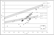
- FIG. 1 is a plot of YS on the x-axis and Kb on the y-axis, and a plot of Co mass% concentration (Co) on the x-axis and YS on the y-axis.
- FIG. 3 is a graph plotting the Co mass% concentration (Co) on the x-axis and Kb on the y-axis. 1 that the copper alloy according to the example satisfies the relationship of 0.43 ⁇ YS + 215 ⁇ Kb ⁇ 0.23 ⁇ YS + 215.
- the formula a ⁇ 55 ⁇ (Co concentration) 2 + 250 ⁇ (Co concentration) + 520 ⁇ YS ⁇ ⁇ 55 ⁇ (Co concentration) 2 + 250 ⁇ (Co concentration) +370
- FIG. 3 shows that the copper alloy according to the example can satisfy the formula A: 60 ⁇ (Co concentration) + 400 ⁇ Kb ⁇ 60 ⁇ (Co concentration) +275.
Landscapes
- Chemical & Material Sciences (AREA)
- Engineering & Computer Science (AREA)
- Materials Engineering (AREA)
- Mechanical Engineering (AREA)
- Metallurgy (AREA)
- Organic Chemistry (AREA)
- Physics & Mathematics (AREA)
- Thermal Sciences (AREA)
- Crystallography & Structural Chemistry (AREA)
- Conductive Materials (AREA)
- Non-Insulated Conductors (AREA)
- Powder Metallurgy (AREA)
Priority Applications (5)
| Application Number | Priority Date | Filing Date | Title |
|---|---|---|---|
| US14/006,735 US9478323B2 (en) | 2011-03-28 | 2012-03-02 | Cu—Si—Co-based copper alloy for electronic materials and method for producing the same |
| EP12764206.4A EP2692878B1 (en) | 2011-03-28 | 2012-03-02 | Cu-si-co-base copper alloy for electronic materials and method for producing same |
| CN201280007476.7A CN103339273B (zh) | 2011-03-28 | 2012-03-02 | 电子材料用Cu-Si-Co系铜合金及其制造方法 |
| PH1/2013/502008A PH12013502008A1 (en) | 2011-03-28 | 2012-03-02 | Cu-co-si-based copper alloy for electronic materials and the method for producing the same |
| KR1020137019104A KR101802009B1 (ko) | 2011-03-28 | 2012-03-02 | 전자 재료용 Cu-Si-Co 계 구리 합금 및 그 제조 방법 |
Applications Claiming Priority (2)
| Application Number | Priority Date | Filing Date | Title |
|---|---|---|---|
| JP2011-070685 | 2011-03-28 | ||
| JP2011070685A JP5451674B2 (ja) | 2011-03-28 | 2011-03-28 | 電子材料用Cu−Si−Co系銅合金及びその製造方法 |
Publications (1)
| Publication Number | Publication Date |
|---|---|
| WO2012132765A1 true WO2012132765A1 (ja) | 2012-10-04 |
Family
ID=46930512
Family Applications (1)
| Application Number | Title | Priority Date | Filing Date |
|---|---|---|---|
| PCT/JP2012/055436 Ceased WO2012132765A1 (ja) | 2011-03-28 | 2012-03-02 | 電子材料用Cu-Si-Co系銅合金及びその製造方法 |
Country Status (8)
| Country | Link |
|---|---|
| US (1) | US9478323B2 (ko) |
| EP (1) | EP2692878B1 (ko) |
| JP (1) | JP5451674B2 (ko) |
| KR (1) | KR101802009B1 (ko) |
| CN (1) | CN103339273B (ko) |
| PH (1) | PH12013502008A1 (ko) |
| TW (2) | TWI448569B (ko) |
| WO (1) | WO2012132765A1 (ko) |
Families Citing this family (10)
| Publication number | Priority date | Publication date | Assignee | Title |
|---|---|---|---|---|
| JP4677505B1 (ja) * | 2010-03-31 | 2011-04-27 | Jx日鉱日石金属株式会社 | 電子材料用Cu−Ni−Si−Co系銅合金及びその製造方法 |
| JP5441876B2 (ja) * | 2010-12-13 | 2014-03-12 | Jx日鉱日石金属株式会社 | 電子材料用Cu−Ni−Si−Co系銅合金及びその製造方法 |
| JP5451674B2 (ja) | 2011-03-28 | 2014-03-26 | Jx日鉱日石金属株式会社 | 電子材料用Cu−Si−Co系銅合金及びその製造方法 |
| JP4799701B1 (ja) * | 2011-03-29 | 2011-10-26 | Jx日鉱日石金属株式会社 | 電子材料用Cu−Co−Si系銅合金条及びその製造方法 |
| JP5595961B2 (ja) * | 2011-03-30 | 2014-09-24 | Jx日鉱日石金属株式会社 | 電子材料用Cu−Ni−Si系銅合金及びその製造方法 |
| US10270142B2 (en) * | 2011-11-07 | 2019-04-23 | Energizer Brands, Llc | Copper alloy metal strip for zinc air anode cans |
| JP5802150B2 (ja) * | 2012-02-24 | 2015-10-28 | 株式会社神戸製鋼所 | 銅合金 |
| KR102104822B1 (ko) | 2017-08-28 | 2020-04-27 | (재)남해마늘연구소 | 마늘 함유 김스낵 제조방법 |
| KR102005332B1 (ko) * | 2019-04-09 | 2019-10-01 | 주식회사 풍산 | 굽힘가공성이 우수한 Cu-Co-Si-Fe-P계 구리 합금 및 그 제조 방법 |
| CN112921257B (zh) * | 2021-01-25 | 2022-02-01 | 安德伦(重庆)材料科技有限公司 | 一种无铍高强度铜合金零件的热处理方法及其成形方法 |
Citations (4)
| Publication number | Priority date | Publication date | Assignee | Title |
|---|---|---|---|---|
| JPH0711363A (ja) * | 1993-06-29 | 1995-01-13 | Toshiba Corp | 高強度・高導電性銅合金部材及びその製造方法 |
| WO2007148712A1 (ja) * | 2006-06-23 | 2007-12-27 | Ngk Insulators, Ltd. | 銅基圧延合金及びその製造方法 |
| JP2008056977A (ja) * | 2006-08-30 | 2008-03-13 | Mitsubishi Electric Corp | 銅合金及びその製造方法 |
| JP2010236071A (ja) | 2009-03-31 | 2010-10-21 | Nippon Mining & Metals Co Ltd | 電子材料用Cu−Co−Si系銅合金及びその製造方法 |
Family Cites Families (30)
| Publication number | Priority date | Publication date | Assignee | Title |
|---|---|---|---|---|
| US7182823B2 (en) | 2002-07-05 | 2007-02-27 | Olin Corporation | Copper alloy containing cobalt, nickel and silicon |
| KR20060120276A (ko) * | 2004-03-12 | 2006-11-24 | 수미도모 메탈 인더스트리즈, 리미티드 | 동 합금 및 그 제조방법 |
| EP1873267B1 (en) | 2005-03-24 | 2014-07-02 | JX Nippon Mining & Metals Corporation | Copper alloy for electronic material |
| JP4068626B2 (ja) | 2005-03-31 | 2008-03-26 | 日鉱金属株式会社 | 電子材料用Cu−Ni−Si−Co−Cr系銅合金及びその製造方法 |
| JP4566048B2 (ja) | 2005-03-31 | 2010-10-20 | 株式会社神戸製鋼所 | 曲げ加工性に優れた高強度銅合金板及びその製造方法 |
| JP4408275B2 (ja) | 2005-09-29 | 2010-02-03 | 日鉱金属株式会社 | 強度と曲げ加工性に優れたCu−Ni−Si系合金 |
| JP2007169765A (ja) | 2005-12-26 | 2007-07-05 | Furukawa Electric Co Ltd:The | 銅合金とその製造方法 |
| JP5028657B2 (ja) | 2006-07-10 | 2012-09-19 | Dowaメタルテック株式会社 | 異方性の少ない高強度銅合金板材およびその製造法 |
| JP5085908B2 (ja) * | 2006-10-03 | 2012-11-28 | Jx日鉱日石金属株式会社 | 電子材料用銅合金及びその製造方法 |
| JP4215093B2 (ja) | 2006-10-26 | 2009-01-28 | 日立電線株式会社 | 圧延銅箔およびその製造方法 |
| JP4285526B2 (ja) | 2006-10-26 | 2009-06-24 | 日立電線株式会社 | 圧延銅箔およびその製造方法 |
| US7789977B2 (en) | 2006-10-26 | 2010-09-07 | Hitachi Cable, Ltd. | Rolled copper foil and manufacturing method thereof |
| JP2008266787A (ja) | 2007-03-28 | 2008-11-06 | Furukawa Electric Co Ltd:The | 銅合金材およびその製造方法 |
| JP4937815B2 (ja) | 2007-03-30 | 2012-05-23 | Jx日鉱日石金属株式会社 | 電子材料用Cu−Ni−Si−Co系銅合金及びその製造方法 |
| JP4466688B2 (ja) * | 2007-07-11 | 2010-05-26 | 日立電線株式会社 | 圧延銅箔 |
| WO2009041197A1 (ja) | 2007-09-28 | 2009-04-02 | Nippon Mining & Metals Co., Ltd. | 電子材料用Cu-Ni-Si-Co系銅合金及びその製造方法 |
| EP2248921A4 (en) | 2008-01-31 | 2011-03-16 | Furukawa Electric Co Ltd | COPPER ALLOY MATERIAL FOR ELECTRICAL / ELECTRONIC COMPONENT AND METHOD FOR PRODUCING THE COPPER ALLOY MATERIAL |
| JP4837697B2 (ja) | 2008-03-31 | 2011-12-14 | Jx日鉱日石金属株式会社 | 電子材料用Cu−Ni−Si−Co系銅合金及びその製造方法 |
| JP4440313B2 (ja) | 2008-03-31 | 2010-03-24 | 日鉱金属株式会社 | 電子材料用Cu−Ni−Si−Co−Cr系合金 |
| JP4596490B2 (ja) | 2008-03-31 | 2010-12-08 | Jx日鉱日石金属株式会社 | 電子材料用Cu−Ni−Si−Co系銅合金及びその製造方法 |
| JP5224415B2 (ja) | 2008-07-31 | 2013-07-03 | 古河電気工業株式会社 | 電気電子部品用銅合金材料とその製造方法 |
| KR101331339B1 (ko) | 2008-12-01 | 2013-11-19 | 제이엑스 닛코 닛세키 킨조쿠 가부시키가이샤 | 전자 재료용 Cu-Ni-Si-Co 계 구리 합금 및 그 제조 방법 |
| JP5261161B2 (ja) | 2008-12-12 | 2013-08-14 | Jx日鉱日石金属株式会社 | Ni−Si−Co系銅合金及びその製造方法 |
| JP5468798B2 (ja) | 2009-03-17 | 2014-04-09 | 古河電気工業株式会社 | 銅合金板材 |
| JP4677505B1 (ja) | 2010-03-31 | 2011-04-27 | Jx日鉱日石金属株式会社 | 電子材料用Cu−Ni−Si−Co系銅合金及びその製造方法 |
| JP4672804B1 (ja) | 2010-05-31 | 2011-04-20 | Jx日鉱日石金属株式会社 | 電子材料用Cu−Co−Si系銅合金及びその製造方法 |
| JP4601085B1 (ja) | 2010-06-03 | 2010-12-22 | Jx日鉱日石金属株式会社 | Cu−Co−Si系銅合金圧延板及びそれを用いた電気部品 |
| JP5441876B2 (ja) * | 2010-12-13 | 2014-03-12 | Jx日鉱日石金属株式会社 | 電子材料用Cu−Ni−Si−Co系銅合金及びその製造方法 |
| JP5451674B2 (ja) | 2011-03-28 | 2014-03-26 | Jx日鉱日石金属株式会社 | 電子材料用Cu−Si−Co系銅合金及びその製造方法 |
| JP4799701B1 (ja) * | 2011-03-29 | 2011-10-26 | Jx日鉱日石金属株式会社 | 電子材料用Cu−Co−Si系銅合金条及びその製造方法 |
-
2011
- 2011-03-28 JP JP2011070685A patent/JP5451674B2/ja active Active
-
2012
- 2012-03-02 KR KR1020137019104A patent/KR101802009B1/ko active Active
- 2012-03-02 US US14/006,735 patent/US9478323B2/en active Active
- 2012-03-02 CN CN201280007476.7A patent/CN103339273B/zh active Active
- 2012-03-02 EP EP12764206.4A patent/EP2692878B1/en active Active
- 2012-03-02 WO PCT/JP2012/055436 patent/WO2012132765A1/ja not_active Ceased
- 2012-03-02 PH PH1/2013/502008A patent/PH12013502008A1/en unknown
- 2012-03-23 TW TW101110071K patent/TWI448569B/zh active
- 2012-03-23 TW TW101110071A patent/TWI516617B/zh active
Patent Citations (4)
| Publication number | Priority date | Publication date | Assignee | Title |
|---|---|---|---|---|
| JPH0711363A (ja) * | 1993-06-29 | 1995-01-13 | Toshiba Corp | 高強度・高導電性銅合金部材及びその製造方法 |
| WO2007148712A1 (ja) * | 2006-06-23 | 2007-12-27 | Ngk Insulators, Ltd. | 銅基圧延合金及びその製造方法 |
| JP2008056977A (ja) * | 2006-08-30 | 2008-03-13 | Mitsubishi Electric Corp | 銅合金及びその製造方法 |
| JP2010236071A (ja) | 2009-03-31 | 2010-10-21 | Nippon Mining & Metals Co Ltd | 電子材料用Cu−Co−Si系銅合金及びその製造方法 |
Non-Patent Citations (1)
| Title |
|---|
| See also references of EP2692878A4 |
Also Published As
| Publication number | Publication date |
|---|---|
| TWI448569B (zh) | 2014-08-11 |
| TWI516617B (zh) | 2016-01-11 |
| EP2692878A4 (en) | 2014-09-10 |
| CN103339273A (zh) | 2013-10-02 |
| JP2012201977A (ja) | 2012-10-22 |
| EP2692878A1 (en) | 2014-02-05 |
| TW201241195A (en) | 2012-10-16 |
| US9478323B2 (en) | 2016-10-25 |
| KR20130109209A (ko) | 2013-10-07 |
| KR101802009B1 (ko) | 2017-11-27 |
| JP5451674B2 (ja) | 2014-03-26 |
| EP2692878B1 (en) | 2018-12-26 |
| PH12013502008A1 (en) | 2016-01-15 |
| US20140014240A1 (en) | 2014-01-16 |
| CN103339273B (zh) | 2016-02-17 |
Similar Documents
| Publication | Publication Date | Title |
|---|---|---|
| JP4677505B1 (ja) | 電子材料用Cu−Ni−Si−Co系銅合金及びその製造方法 | |
| JP5451674B2 (ja) | 電子材料用Cu−Si−Co系銅合金及びその製造方法 | |
| JP5441876B2 (ja) | 電子材料用Cu−Ni−Si−Co系銅合金及びその製造方法 | |
| JP4799701B1 (ja) | 電子材料用Cu−Co−Si系銅合金条及びその製造方法 | |
| JP5506806B2 (ja) | 電子材料用Cu−Ni−Si−Co系銅合金及びその製造方法 | |
| JP6385383B2 (ja) | 銅合金板材および銅合金板材の製造方法 | |
| WO2009122869A1 (ja) | 電子材料用Cu-Ni-Si-Co系銅合金及びその製造方法 | |
| JP6222885B2 (ja) | 電子材料用Cu−Ni−Si−Co系銅合金 | |
| JP2012229467A (ja) | 電子材料用Cu−Ni−Si系銅合金 | |
| JP5524901B2 (ja) | 電子材料用Cu−Ni−Si−Co系銅合金 | |
| JP2016183418A (ja) | 電子材料用Cu−Ni−Si−Co系銅合金 | |
| JP5595961B2 (ja) | 電子材料用Cu−Ni−Si系銅合金及びその製造方法 | |
| JP2012229469A (ja) | 電子材料用Cu−Si−Co系銅合金及びその製造方法 | |
| JP5623960B2 (ja) | 電子材料用Cu−Ni−Si系銅合金条及びその製造方法 |
Legal Events
| Date | Code | Title | Description |
|---|---|---|---|
| WWE | Wipo information: entry into national phase |
Ref document number: 201280007476.7 Country of ref document: CN |
|
| 121 | Ep: the epo has been informed by wipo that ep was designated in this application |
Ref document number: 12764206 Country of ref document: EP Kind code of ref document: A1 |
|
| ENP | Entry into the national phase |
Ref document number: 20137019104 Country of ref document: KR Kind code of ref document: A |
|
| WWE | Wipo information: entry into national phase |
Ref document number: 14006735 Country of ref document: US |
|
| NENP | Non-entry into the national phase |
Ref country code: DE |
|
| WWE | Wipo information: entry into national phase |
Ref document number: 2012764206 Country of ref document: EP |