WO2012133367A1 - 導電積層体およびタッチパネル - Google Patents
導電積層体およびタッチパネル Download PDFInfo
- Publication number
- WO2012133367A1 WO2012133367A1 PCT/JP2012/057860 JP2012057860W WO2012133367A1 WO 2012133367 A1 WO2012133367 A1 WO 2012133367A1 JP 2012057860 W JP2012057860 W JP 2012057860W WO 2012133367 A1 WO2012133367 A1 WO 2012133367A1
- Authority
- WO
- WIPO (PCT)
- Prior art keywords
- layer
- conductive
- protective layer
- mass
- cross
- Prior art date
- Legal status (The legal status is an assumption and is not a legal conclusion. Google has not performed a legal analysis and makes no representation as to the accuracy of the status listed.)
- Ceased
Links
Images



Classifications
-
- C—CHEMISTRY; METALLURGY
- C08—ORGANIC MACROMOLECULAR COMPOUNDS; THEIR PREPARATION OR CHEMICAL WORKING-UP; COMPOSITIONS BASED THEREON
- C08J—WORKING-UP; GENERAL PROCESSES OF COMPOUNDING; AFTER-TREATMENT NOT COVERED BY SUBCLASSES C08B, C08C, C08F, C08G or C08H
- C08J7/00—Chemical treatment or coating of shaped articles made of macromolecular substances
- C08J7/04—Coating
- C08J7/043—Improving the adhesiveness of the coatings per se, e.g. forming primers
-
- B—PERFORMING OPERATIONS; TRANSPORTING
- B32—LAYERED PRODUCTS
- B32B—LAYERED PRODUCTS, i.e. PRODUCTS BUILT-UP OF STRATA OF FLAT OR NON-FLAT, e.g. CELLULAR OR HONEYCOMB, FORM
- B32B27/00—Layered products comprising a layer of synthetic resin
- B32B27/06—Layered products comprising a layer of synthetic resin as the main or only constituent of a layer, which is next to another layer of the same or of a different material
- B32B27/08—Layered products comprising a layer of synthetic resin as the main or only constituent of a layer, which is next to another layer of the same or of a different material of synthetic resin
-
- B—PERFORMING OPERATIONS; TRANSPORTING
- B32—LAYERED PRODUCTS
- B32B—LAYERED PRODUCTS, i.e. PRODUCTS BUILT-UP OF STRATA OF FLAT OR NON-FLAT, e.g. CELLULAR OR HONEYCOMB, FORM
- B32B27/00—Layered products comprising a layer of synthetic resin
- B32B27/12—Layered products comprising a layer of synthetic resin next to a fibrous or filamentary layer
-
- B—PERFORMING OPERATIONS; TRANSPORTING
- B32—LAYERED PRODUCTS
- B32B—LAYERED PRODUCTS, i.e. PRODUCTS BUILT-UP OF STRATA OF FLAT OR NON-FLAT, e.g. CELLULAR OR HONEYCOMB, FORM
- B32B27/00—Layered products comprising a layer of synthetic resin
- B32B27/30—Layered products comprising a layer of synthetic resin comprising vinyl (co)polymers; comprising acrylic (co)polymers
- B32B27/302—Layered products comprising a layer of synthetic resin comprising vinyl (co)polymers; comprising acrylic (co)polymers comprising aromatic vinyl (co)polymers, e.g. styrenic (co)polymers
-
- B—PERFORMING OPERATIONS; TRANSPORTING
- B32—LAYERED PRODUCTS
- B32B—LAYERED PRODUCTS, i.e. PRODUCTS BUILT-UP OF STRATA OF FLAT OR NON-FLAT, e.g. CELLULAR OR HONEYCOMB, FORM
- B32B27/00—Layered products comprising a layer of synthetic resin
- B32B27/30—Layered products comprising a layer of synthetic resin comprising vinyl (co)polymers; comprising acrylic (co)polymers
- B32B27/308—Layered products comprising a layer of synthetic resin comprising vinyl (co)polymers; comprising acrylic (co)polymers comprising acrylic (co)polymers
-
- B—PERFORMING OPERATIONS; TRANSPORTING
- B32—LAYERED PRODUCTS
- B32B—LAYERED PRODUCTS, i.e. PRODUCTS BUILT-UP OF STRATA OF FLAT OR NON-FLAT, e.g. CELLULAR OR HONEYCOMB, FORM
- B32B27/00—Layered products comprising a layer of synthetic resin
- B32B27/36—Layered products comprising a layer of synthetic resin comprising polyesters
-
- B—PERFORMING OPERATIONS; TRANSPORTING
- B32—LAYERED PRODUCTS
- B32B—LAYERED PRODUCTS, i.e. PRODUCTS BUILT-UP OF STRATA OF FLAT OR NON-FLAT, e.g. CELLULAR OR HONEYCOMB, FORM
- B32B7/00—Layered products characterised by the relation between layers; Layered products characterised by the relative orientation of features between layers, or by the relative values of a measurable parameter between layers, i.e. products comprising layers having different physical, chemical or physicochemical properties; Layered products characterised by the interconnection of layers
- B32B7/04—Interconnection of layers
- B32B7/12—Interconnection of layers using interposed adhesives or interposed materials with bonding properties
-
- C—CHEMISTRY; METALLURGY
- C08—ORGANIC MACROMOLECULAR COMPOUNDS; THEIR PREPARATION OR CHEMICAL WORKING-UP; COMPOSITIONS BASED THEREON
- C08J—WORKING-UP; GENERAL PROCESSES OF COMPOUNDING; AFTER-TREATMENT NOT COVERED BY SUBCLASSES C08B, C08C, C08F, C08G or C08H
- C08J7/00—Chemical treatment or coating of shaped articles made of macromolecular substances
- C08J7/04—Coating
- C08J7/042—Coating with two or more layers, where at least one layer of a composition contains a polymer binder
- C08J7/0423—Coating with two or more layers, where at least one layer of a composition contains a polymer binder with at least one layer of inorganic material and at least one layer of a composition containing a polymer binder
-
- C—CHEMISTRY; METALLURGY
- C08—ORGANIC MACROMOLECULAR COMPOUNDS; THEIR PREPARATION OR CHEMICAL WORKING-UP; COMPOSITIONS BASED THEREON
- C08J—WORKING-UP; GENERAL PROCESSES OF COMPOUNDING; AFTER-TREATMENT NOT COVERED BY SUBCLASSES C08B, C08C, C08F, C08G or C08H
- C08J7/00—Chemical treatment or coating of shaped articles made of macromolecular substances
- C08J7/04—Coating
- C08J7/044—Forming conductive coatings; Forming coatings having anti-static properties
-
- C—CHEMISTRY; METALLURGY
- C08—ORGANIC MACROMOLECULAR COMPOUNDS; THEIR PREPARATION OR CHEMICAL WORKING-UP; COMPOSITIONS BASED THEREON
- C08J—WORKING-UP; GENERAL PROCESSES OF COMPOUNDING; AFTER-TREATMENT NOT COVERED BY SUBCLASSES C08B, C08C, C08F, C08G or C08H
- C08J7/00—Chemical treatment or coating of shaped articles made of macromolecular substances
- C08J7/04—Coating
- C08J7/046—Forming abrasion-resistant coatings; Forming surface-hardening coatings
-
- G—PHYSICS
- G06—COMPUTING OR CALCULATING; COUNTING
- G06F—ELECTRIC DIGITAL DATA PROCESSING
- G06F3/00—Input arrangements for transferring data to be processed into a form capable of being handled by the computer; Output arrangements for transferring data from processing unit to output unit, e.g. interface arrangements
- G06F3/01—Input arrangements or combined input and output arrangements for interaction between user and computer
- G06F3/03—Arrangements for converting the position or the displacement of a member into a coded form
- G06F3/041—Digitisers, e.g. for touch screens or touch pads, characterised by the transducing means
-
- G—PHYSICS
- G06—COMPUTING OR CALCULATING; COUNTING
- G06F—ELECTRIC DIGITAL DATA PROCESSING
- G06F3/00—Input arrangements for transferring data to be processed into a form capable of being handled by the computer; Output arrangements for transferring data from processing unit to output unit, e.g. interface arrangements
- G06F3/01—Input arrangements or combined input and output arrangements for interaction between user and computer
- G06F3/03—Arrangements for converting the position or the displacement of a member into a coded form
- G06F3/041—Digitisers, e.g. for touch screens or touch pads, characterised by the transducing means
- G06F3/0412—Digitisers structurally integrated in a display
-
- G—PHYSICS
- G06—COMPUTING OR CALCULATING; COUNTING
- G06F—ELECTRIC DIGITAL DATA PROCESSING
- G06F3/00—Input arrangements for transferring data to be processed into a form capable of being handled by the computer; Output arrangements for transferring data from processing unit to output unit, e.g. interface arrangements
- G06F3/01—Input arrangements or combined input and output arrangements for interaction between user and computer
- G06F3/03—Arrangements for converting the position or the displacement of a member into a coded form
- G06F3/041—Digitisers, e.g. for touch screens or touch pads, characterised by the transducing means
- G06F3/045—Digitisers, e.g. for touch screens or touch pads, characterised by the transducing means using resistive elements, e.g. a single continuous surface or two parallel surfaces put in contact
-
- H—ELECTRICITY
- H01—ELECTRIC ELEMENTS
- H01B—CABLES; CONDUCTORS; INSULATORS; SELECTION OF MATERIALS FOR THEIR CONDUCTIVE, INSULATING OR DIELECTRIC PROPERTIES
- H01B5/00—Non-insulated conductors or conductive bodies characterised by their form
- H01B5/14—Non-insulated conductors or conductive bodies characterised by their form comprising conductive layers or films on insulating-supports
-
- H—ELECTRICITY
- H05—ELECTRIC TECHNIQUES NOT OTHERWISE PROVIDED FOR
- H05K—PRINTED CIRCUITS; CASINGS OR CONSTRUCTIONAL DETAILS OF ELECTRIC APPARATUS; MANUFACTURE OF ASSEMBLAGES OF ELECTRICAL COMPONENTS
- H05K1/00—Printed circuits
- H05K1/02—Details
-
- B—PERFORMING OPERATIONS; TRANSPORTING
- B32—LAYERED PRODUCTS
- B32B—LAYERED PRODUCTS, i.e. PRODUCTS BUILT-UP OF STRATA OF FLAT OR NON-FLAT, e.g. CELLULAR OR HONEYCOMB, FORM
- B32B2260/00—Layered product comprising an impregnated, embedded, or bonded layer wherein the layer comprises an impregnation, embedding, or binder material
- B32B2260/02—Composition of the impregnated, bonded or embedded layer
- B32B2260/021—Fibrous or filamentary layer
-
- B—PERFORMING OPERATIONS; TRANSPORTING
- B32—LAYERED PRODUCTS
- B32B—LAYERED PRODUCTS, i.e. PRODUCTS BUILT-UP OF STRATA OF FLAT OR NON-FLAT, e.g. CELLULAR OR HONEYCOMB, FORM
- B32B2260/00—Layered product comprising an impregnated, embedded, or bonded layer wherein the layer comprises an impregnation, embedding, or binder material
- B32B2260/04—Impregnation, embedding, or binder material
- B32B2260/046—Synthetic resin
-
- B—PERFORMING OPERATIONS; TRANSPORTING
- B32—LAYERED PRODUCTS
- B32B—LAYERED PRODUCTS, i.e. PRODUCTS BUILT-UP OF STRATA OF FLAT OR NON-FLAT, e.g. CELLULAR OR HONEYCOMB, FORM
- B32B2262/00—Composition or structural features of fibres which form a fibrous or filamentary layer or are present as additives
- B32B2262/10—Inorganic fibres
- B32B2262/103—Metal fibres
-
- B—PERFORMING OPERATIONS; TRANSPORTING
- B32—LAYERED PRODUCTS
- B32B—LAYERED PRODUCTS, i.e. PRODUCTS BUILT-UP OF STRATA OF FLAT OR NON-FLAT, e.g. CELLULAR OR HONEYCOMB, FORM
- B32B2262/00—Composition or structural features of fibres which form a fibrous or filamentary layer or are present as additives
- B32B2262/10—Inorganic fibres
- B32B2262/106—Carbon fibres, e.g. graphite fibres
-
- B—PERFORMING OPERATIONS; TRANSPORTING
- B32—LAYERED PRODUCTS
- B32B—LAYERED PRODUCTS, i.e. PRODUCTS BUILT-UP OF STRATA OF FLAT OR NON-FLAT, e.g. CELLULAR OR HONEYCOMB, FORM
- B32B2307/00—Properties of the layers or laminate
- B32B2307/20—Properties of the layers or laminate having particular electrical or magnetic properties, e.g. piezoelectric
- B32B2307/202—Conductive
-
- B—PERFORMING OPERATIONS; TRANSPORTING
- B32—LAYERED PRODUCTS
- B32B—LAYERED PRODUCTS, i.e. PRODUCTS BUILT-UP OF STRATA OF FLAT OR NON-FLAT, e.g. CELLULAR OR HONEYCOMB, FORM
- B32B2307/00—Properties of the layers or laminate
- B32B2307/50—Properties of the layers or laminate having particular mechanical properties
- B32B2307/584—Scratch resistance
-
- B—PERFORMING OPERATIONS; TRANSPORTING
- B32—LAYERED PRODUCTS
- B32B—LAYERED PRODUCTS, i.e. PRODUCTS BUILT-UP OF STRATA OF FLAT OR NON-FLAT, e.g. CELLULAR OR HONEYCOMB, FORM
- B32B2457/00—Electrical equipment
- B32B2457/20—Displays, e.g. liquid crystal displays, plasma displays
- B32B2457/202—LCD, i.e. liquid crystal displays
-
- B—PERFORMING OPERATIONS; TRANSPORTING
- B32—LAYERED PRODUCTS
- B32B—LAYERED PRODUCTS, i.e. PRODUCTS BUILT-UP OF STRATA OF FLAT OR NON-FLAT, e.g. CELLULAR OR HONEYCOMB, FORM
- B32B2457/00—Electrical equipment
- B32B2457/20—Displays, e.g. liquid crystal displays, plasma displays
- B32B2457/206—Organic displays, e.g. OLED
-
- B—PERFORMING OPERATIONS; TRANSPORTING
- B32—LAYERED PRODUCTS
- B32B—LAYERED PRODUCTS, i.e. PRODUCTS BUILT-UP OF STRATA OF FLAT OR NON-FLAT, e.g. CELLULAR OR HONEYCOMB, FORM
- B32B2457/00—Electrical equipment
- B32B2457/20—Displays, e.g. liquid crystal displays, plasma displays
- B32B2457/208—Touch screens
-
- C—CHEMISTRY; METALLURGY
- C08—ORGANIC MACROMOLECULAR COMPOUNDS; THEIR PREPARATION OR CHEMICAL WORKING-UP; COMPOSITIONS BASED THEREON
- C08J—WORKING-UP; GENERAL PROCESSES OF COMPOUNDING; AFTER-TREATMENT NOT COVERED BY SUBCLASSES C08B, C08C, C08F, C08G or C08H
- C08J2433/00—Characterised by the use of homopolymers or copolymers of compounds having one or more unsaturated aliphatic radicals, each having only one carbon-to-carbon double bond, and only one being terminated by only one carboxyl radical, or of salts, anhydrides, esters, amides, imides, or nitriles thereof; Derivatives of such polymers
-
- C—CHEMISTRY; METALLURGY
- C08—ORGANIC MACROMOLECULAR COMPOUNDS; THEIR PREPARATION OR CHEMICAL WORKING-UP; COMPOSITIONS BASED THEREON
- C08J—WORKING-UP; GENERAL PROCESSES OF COMPOUNDING; AFTER-TREATMENT NOT COVERED BY SUBCLASSES C08B, C08C, C08F, C08G or C08H
- C08J2475/00—Characterised by the use of polyureas or polyurethanes; Derivatives of such polymers
- C08J2475/04—Polyurethanes
- C08J2475/14—Polyurethanes having carbon-to-carbon unsaturated bonds
Definitions
- the present invention relates to a conductive laminate. More specifically, the present invention relates to a conductive laminate used for display members such as touch panels, liquid crystal displays, organic electroluminescence, and electronic paper, and electrode members such as solar cell modules. Furthermore, the present invention relates to a touch panel using a conductive laminate.
- An electrode member is used for the touch panel, and a plurality of electrode members are used for the touch panel that enables complicated operations.
- a plurality of steps for example, a step of forming a desired pattern on the surface of the conductive layer of the electrode members, a step of bonding the electrode members together by pressing and heating, etc.
- the electrode member to be used is subjected to various energy stresses.
- a conductive laminate in which a layer made of a polymer compound having a functional group such as an amino group is laminated on a conductive thin film layer provided on a polymer substrate Patent Document 1.
- a conductive laminate in which a layer made of a polymer compound such as a cyano group is laminated on a conductive thin film layer made of a metal thin film or a conductive polymer thin film provided on a plastic substrate Patent Document 2
- a polymer Conductive lamination in which a layer made of a polymer compound having a cationic functional quaternary ammonium base or sulfone group as a hydrophilic functional group is laminated on a conductive layer containing a needle-like conductive metal oxide provided on a substrate
- Various layers such as polyester alkoxide hydrolyzate, silicone compound, etc.
- Patent Document 3 conductive layer containing spherical metal fine particles.
- transparent conductive film Patent Document 4
- specific functional group or a conductive laminate a layer comprising the polymer compound laminated to the conductive thin film layer having a skeleton structure has been proposed.
- CNT carbon nanotubes
- Patent Document 5 a conductive laminate in which a thin film layer made of polyester resin and CNT is laminated on one or both sides of a polyester film substrate (Patent Document 6), and various vinyl groups and vinylidene groups as carbon-carbon double bonds.
- a conductive laminate (Patent Documents 7, 8, and 9) is also proposed in which a thin film layer made of a resin and CNTs is laminated on one or both sides of a substrate.
- Patent Document 10 a conductive laminate using metal nanowires such as silver as a linear structure of conductive components has also been proposed (Patent Document 10), and a conductive laminate using these conductive linear structures is proposed.
- a touch panel configured by using the touch panel has also been proposed (Patent Documents 10 and 11).
- the layer laminated on the conductive layer has a functional group such as an amino group, a cyano group, a cationic quaternary ammonium base, or a sulfone group.
- a functional group such as an amino group, a cyano group, a cationic quaternary ammonium base, or a sulfone group.
- the polymer compound is used as a component, the durability against heat and humidity is inferior, so that the substrate is damaged and causes problems such as yellowing of the substrate.
- the base material is a resin base material
- a relatively low molecular weight component called an oligomer existing in the base material is heated by a plurality of steps when the electrode member is processed into a product.
- the present invention is intended to provide a conductive laminate having good durability against heat.
- the present invention employs the following configuration. That is, a conductive laminate satisfying the following (i) to (iv) in which a crosslinked layer is laminated on one surface of a substrate, and a conductive layer and a protective layer are laminated on the other surface of the substrate.
- the crosslinked layer is composed of a crosslinked polymer including a structure in which a compound having a carbon-carbon double bond group contributing to two or more polymerization reactions in the structure undergoes a polymerization reaction;
- the mass content of the unit structure (> C ⁇ C ⁇ : formula 24) of the carbon-carbon double bond group in the structure derived from the carbon-carbon double bond group with respect to the mass is 9 to 26 mass%.
- the crosslinked layer has a thickness of 50 nm to 1 ⁇ m.
- the conductive layer includes a conductive component having a network structure including a linear structure.
- the protective layer has an average thickness t of 70 nm to 1 ⁇ m.
- the present invention also includes a touch panel using the above conductive laminate.
- a conductive laminate having good durability against heat can be provided.
- the conductive laminate of the present invention can be suitably used for touch panel applications.
- the conductive laminate of the present invention can also be suitably used for electrode members used in displays such as liquid crystal displays, organic electroluminescence displays, electronic paper, and solar cell modules.
- the cross-linked layer 4 is laminated on one surface of the substrate 1, and the conductive layer 2 and the protective layer 3 are laminated on the other surface of the substrate. It has a configuration. Each layer satisfies the following conditions (i) to (iv).
- the crosslinked layer is composed of a crosslinked polymer including a structure in which a compound having a carbon-carbon double bond group contributing to two or more polymerization reactions in the structure undergoes a polymerization reaction, and the total mass of the crosslinked layer
- the mass content of the unit structure (> C ⁇ C ⁇ : formula 24) of the carbon-carbon double bond group in the structure derived from the carbon-carbon double bond group is 9 to 26 mass%.
- the crosslinked layer has a thickness of 50 nm to 1 ⁇ m.
- the conductive layer includes a conductive component having a network structure including a linear structure.
- the protective layer has an average thickness t of 70 nm to 1 ⁇ m.
- the conductive layer in the present invention is a layer containing a conductive component having a network structure made of a linear structure.
- the conductive component has a network structure including a linear structure, when the amount of the linear structure is equal to or less than a certain value, there may be a region where the linear structure does not exist in the plane. Even if such a region exists, if a linear structure exists continuously and uniformly in the plane and conductivity can be exhibited between any two points by forming a network, a conductive layer is formed. It shall be. That is, in such a case, a layered region formed by a linear structure (including a region where no scattered linear structure exists) is defined as a conductive layer.
- the surface of the protective layer is present on the substrate side compared to the surface of the linear structure (when viewed from the protective layer side, There may be a case where the linear structure is partially buried.
- the conductive layer is defined from the surface of the substrate to the outermost layer of the linear structure.
- the protective layer is defined as the protective layer from the outermost layer of the linear structure to the outermost surface of the laminate in the part with the linear structure, and from the surface of the substrate to the outermost surface of the laminate in the part without the linear structure.
- the crosslinked layer is obtained by polymerizing a composition containing a compound having a carbon-carbon double bond group that contributes to two or more polymerization reactions in the structure in the above specific range. Since it is obtained and forms a dense cross-linked structure, it is presumed that the free volume of the cross-linked layer is reduced and the movement of the oligomer is suppressed.
- a structure in which a compound having a carbon-carbon double bond group contributing to the polymerization reaction with respect to the total mass of the cross-linked layer is used as an index of the density of the cross-linked structure of the cross-linked layer (hereinafter referred to as carbon-carbon double bond group).
- the cross-linking unit structure mass content is less than 9% by mass, the number of cross-linking points starting from the structure derived from the carbon-carbon double bond group is reduced, and the density of the cross-linked structure of the cross-linked layer is reduced. It is presumed that the effect of reducing the volume is not sufficient, and the effect of suppressing the migration of the oligomer cannot be obtained.
- the cross-linking unit structure mass content is larger than 26% by mass, there are too many cross-linking points, and stress relaxation in the cross-linked layer accompanying cross-linking cannot be performed, and for example, curling or flatness of the conductive laminate is deteriorated. Invite.
- the network structure of the linear structures in the conductive layer is defective (for example, due to defective conductive contacts between the linear structures or bending of the linear structures themselves) Damage) and the like, the electrical conductivity decreases, making it difficult to achieve a desired surface resistance value. Therefore, when the cross-linking unit structure mass content is 9% by mass to 26% by mass, the cross-linked structure is densely formed, the free volume of the cross-linked layer is reduced, and the conductivity that satisfies both suppression of oligomer precipitation and surface conductivity is achieved. It can be a laminate.
- the cross-linking unit structure mass content is preferably in the range of 19% by mass to 24% by mass, and more preferably in the range of 21% by mass to 24% by mass, the effect of suppressing oligomer precipitation is easily obtained, and the thickness of the cross-linked layer is increased. Is preferable because the thickness can be reduced.
- the thickness of the cross-linked layer is 50 nm to 1 ⁇ m.
- a conductive layer is formed on the surface opposite to the cross-linked layer through the base material.
- the conductive layer is a layer containing a conductive component having a network structure made of a linear structure.
- the linear structure forms a network structure with respect to the conductive layer surface, so that the linear structure is present even if there is a sparse part where the linear structure does not exist. Since electricity flows through the portion where the body exists, the resistance value of the surface of the conductive laminate as a whole is sufficiently low and there is no problem at a practical level.
- the conductive layer contains a conductive component having a network structure composed of a linear structure.
- a step of forming a desired pattern as an electrode member on the conductive layer is necessary. That is, the conductive layer has a conductive component that remains conductive by patterning (hereinafter referred to as a conductive region) and a region that is electrically insulated after the conductive component is removed (hereinafter referred to as an insulating region). And are formed. If the insulating region has insufficient electrical insulation, problems such as a short circuit occur when used as an electrode member, and it cannot be used as an electrode member.
- the conductive layer is made of a metal or a conductive metal oxide such as ITO
- the conductivity of the conductive region but for the insulating region, sufficient insulation is required unless all the conductive layers are removed. Therefore, the base material must be exposed in the insulating region. In that case, for the conductive region, the conductive layer prevents oligomer precipitation to some extent, but for the insulating region, oligomer precipitation cannot be suppressed.
- the conductive component is a linear structure, it is presumed that the effect of suppressing oligomer precipitation and electrical insulation are easily compatible due to the effects described later.
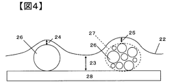
- the protective layer thickness 23 in the portion where the linear structure does not exist is thicker than the protective layer thickness 24 or 25 in the portion where the linear structure exists as shown in FIG. Become.
- the protective layer is eroded by the removal component (for example, acid component or base component) in the removal agent. Since the speed does not change depending on the location of the protective layer, when the protective layer in the portion where the thin linear structure exists is removed, the protective layer remains in the other portions.
- the removal component that has penetrated into the protective layer reaches the linear structure in a short time in the portion where the linear structure exists, and the erosion selectively proceeds in the long axis direction of the linear structure, thereby
- the rate at which the structure is removed is greater than the rate at which the surrounding protective layer is removed. Therefore, at the time of patterning, only the linear structure can be removed leaving the protective layer. That is, it is presumed that oligomer precipitation can be suppressed because the surface of the base material is covered with the protective layer without being exposed even in the insulating region from which the linear structure as the conductive component is removed.
- the average thickness t of the protective layer is less than 70 nm, the time until the removal component completely penetrates into the protection layer and the linear structure is shortened. Since only the linear structure cannot be selectively removed and the protective layer is also removed together, the base material is easily exposed and the effect of suppressing oligomer precipitation cannot be obtained.
- the average thickness t of the protective layer is 70 nm or more, the protective layer can be left even after patterning, and oligomer precipitation can be suppressed.
- the average thickness t of the protective layer is greater than 1 ⁇ m, the conductive structure (in the present invention, the side on which the conductive layer and the protective layer are laminated) has a reduced linear structure on the surface layer.
- the average thickness t of the protective layer is 1 ⁇ m or less, it is possible to obtain a conductive laminate that does not hinder the conductivity of the conductive component and does not have an abnormal increase in resistance value or poor conduction.
- the average thickness t of the protective layer is preferably 100 nm to 500 nm, more preferably 100 nm to 400 nm, and most preferably 150 nm to 350 nm.
- the protective layer When the average thickness t of the protective layer is 100 nm to 500 nm, the protective layer remains sufficiently after patterning, and the effect of preventing oligomer precipitation is high. When the average thickness t of the protective layer is from 100 nm to 400 nm, it is easier to obtain a low surface resistance value while having the effect of preventing oligomer precipitation. Further, when the average thickness t of the protective layer is 150 nm to 350 nm, the conductive laminate tends to have a low surface resistance stably even if the conductivity of the conductive component is somewhat high.
- the average thickness t of the protective layer is obtained as follows. After embedding the observation part of the sample with ice or an epoxy resin that has a stronger adhesion than ice, use a rotary microtome manufactured by Nihon Microtome Research Co., Ltd. and set a diamond knife at a 3 ° knife inclination angle. And cut in a direction perpendicular to the film plane. Next, the cross section of the obtained film was appropriately adjusted in image contrast using a field emission scanning electron microscope (JSM-6700-F manufactured by JEOL Ltd.) at an acceleration voltage of 3.0 kV and an observation magnification of 10,000 to 100,000. Adjust and observe.
- JSM-6700-F manufactured by JEOL Ltd.
- the protective layer thickness 23 portion where the protective layer thickness is thick
- An arbitrary five points of the protective layer thickness 25 (the portion where the protective layer thickness is thin) on the apex of the aggregate composed of the shaped structures are measured (calculated from the magnification) and averaged to obtain the average thickness t of the protective layer. .
- a magnification that can secure 3 significant figures is selected, and the value is calculated by rounding off the 4th digit.
- the cross-linked layer suppresses oligomer precipitation on the surface of one side of the substrate
- the protective layer suppresses oligomer precipitation on the other side of the substrate. is doing.
- the protective layer remains and the surface of the base material is not exposed, so that precipitation of oligomers during heating can be effectively suppressed and good durability against heat can be achieved.
- the crosslinked layer in the present invention includes a structure derived from a carbon-carbon double bond group.
- the functional group containing a carbon-carbon double bond group that contributes to the polymerization reaction include allyl group, acryloyl group, methacryloyl group, acryloyloxy group, methacryloyloxy group, methacryl group, acrylamide group, methacrylamide group, and arylidene group. , Allylidine group, vinyl ether group and the like.
- a halogen element for example, fluorine or chlorine
- a substituent having an aromatic ring for example, a phenyl group or a naphthyl group
- a vinyl fluoride group Vinylidene fluoride groups, vinyl chloride groups, vinylidene chloride groups, styryl groups having a phenyl group (benzene ring) as an aromatic ring, isopropenyl group, isopentenyl group, butadienyl group (for example, CH 2 ⁇ C (R 1 ) —C (R 2 ) ⁇ CH—, CH 2 ⁇ C (R 1 ) —C ( ⁇ CH 2 ) — (R 1 , R 2 is H or CH 3 )))
- a group selected from a group and a methacryloyloxy group can be preferably used.
- a carbonyl group having higher stability than an acryloyloxy group having an ester group (—COO—) that may become a hydrolysis base point due to moisture in the air that has obtained thermal energy during heating a carbonyl group having only (—CO—) is most preferred because it is more durable against heat and can easily provide an oligomer precipitation inhibiting effect.
- Examples of the compound having a carbon-carbon double bond group that contributes to the polymerization reaction in the structure include pentaerythritol triacrylate, pentaerythritol trimethacrylate, pentaerythritol tetraacrylate, pentaerythritol tetramethacrylate, pentaerythritol ethoxy.
- Triacrylate pentaerythritol ethoxytrimethacrylate, pentaerythritol ethoxytetraacrylate, pentaerythritol ethoxytetramethacrylate, dipentaerythritol triacrylate, dipentaerythritol trimethacrylate, dipentaerythritol tetraacrylate, dipentaerythritol tetramethacrylate, dipentaerythritol pentaacrylate Dipentaellis Tall pentamethacrylate, dipentaerythritol hexaacrylate, dipentaerythritol hexamethacrylate, trimethylolpropane triacrylate, trimethylolpropane trimethacrylate, trimethylolpropane ethoxytriacrylate, trimethylolpropane ethoxytrimethacrylate, ditrimethylolpropane triacrylate,
- triacrylate, trimethacrylate, tetraacrylate, tetramethacrylate, pentaacrylate, pentamethacrylate, hexaacrylate, hexahexacyclic skeleton such as cyclopropane ring, cyclobutane ring, cyclopentane ring and cyclohexane ring are partly included in the molecular structure.
- a methacrylate etc. are also mentioned.
- a compound obtained by modifying a partial structure of the above compound for example, 2-hydroxypropanoic acid-modified pentaerythritol triacrylate modified with 2-hydroxypropanoic acid, 2-hydroxypropanoic acid-modified pentaerythritol trimethacrylate, 2-hydroxypropanoic acid Modified pentaerythritol tetraacrylate, 2-hydroxypropanoic acid modified pentaerythritol tetramethacrylate, silicone triacrylate with silicone skeleton, silicone trimethacrylate, silicone tetraacrylate, silicone tetramethacrylate, silicone pentaacrylate, silicone pentamethacrylate, silicone hexa Examples include acrylate and silicone hexamethacrylate.
- those having other skeletons together with vinyl groups and / or vinylidene groups in the skeleton such as urethane triacrylate, urethane trimethacrylate, urethane tetraacrylate, urethane tetramethacrylate, urethane pentaacrylate, urethane pentamethacrylate, urethane hexaacrylate having a urethane skeleton , Urethane hexamethacrylate; polyether triacrylate having ether skeleton, polyether trimethacrylate, polyether tetraacrylate, polyether tetramethacrylate, polyether pentaacrylate, polyether pentamethacrylate, polyether hexaacrylate, polyether hexamethacrylate; epoxy Epoxy triacrylate having a skeleton derived from Xyltrimethacrylate, Epoxytetraacrylate, Epoxytetramethacrylate, Epoxypenta
- compositions in which one or more of these are mixed, or an oligomer in which two or more of these are copolymerized can be used. It is not something.
- Commercially available products include, for example, the light acrylate series, light ester series, epoxy ester series, urethane acrylate AH series, urethane acrylate AT series, urethane acrylate UA series, manufactured by Kyoeisha Chemical Co., Ltd., Daicel Cytec Co., Ltd.
- EBECRYL registered trademark
- PETIA PETIA
- TMPTA TMPEOTA
- OTA 480 DPHA
- PETA-K Furu Cure (registered trademark) series manufactured by Soken Chemical Co., Ltd., "LIODURAS (Ryoduras) manufactured by Toyo Ink Manufacturing Co., Ltd. ) (Registered trademark) "series, Forseed (registered trademark) series manufactured by China Paint Co., Ltd., EXP series manufactured by Matsui Kagaku Co., Ltd., and the like.
- the cross-linking unit structure mass content of the cross-linking layer is determined as follows. First, the crosslinked layer is peeled off from the sample, and the crosslinked layer is dissolved in a soluble solvent. If necessary, select a separable method from general chromatography such as silica gel column chromatography, gel permeation chromatography, liquid high-performance chromatography, etc. After separation and purification, it is subjected to the following qualitative analysis and quantitative analysis.
- the analysis method is first performed by combining the analysis methods of the group (1), and when there is a component that cannot be detected by the analysis method, the analysis method of the group (2) is combined.
- the analysis method for each group is applied in order from the one shown above, and the following method is used when there are components that cannot be detected by the previous method.
- the method described above is used preferentially, and the method capable of measuring with fewer combinations is preferentially applied.
- XRD X-ray diffraction
- ND neutron diffraction
- LEED low-energy electron diffraction
- RHEED fast reflection electron diffraction
- AAS ultraviolet photoelectron spectroscopy
- UPS ultraviolet photoelectron spectroscopy
- AES Auger electron spectroscopy
- XPS X-ray photoelectron spectroscopy
- XRF X-ray fluorescence elemental analysis
- ICP-AES inductively coupled plasma emission spectroscopy
- EPMA electron microanalysis
- PIXE Charged particle excitation X-ray spectroscopy
- RBS or LEIS low energy ion scattering spectroscopy
- MEIS medium energy ion scattering spectroscopy
- ISS or HEIS high energy ion scattering spectroscopy
- GPC gel permeation chromatography
- TEM-EDX scanning electron microscope-energy dispersive X-ray Light analysis
- TBE 1,1,2,2-tetrabromoethane
- the thickness of the cross-linked layer in the conductive laminate of the present invention is 50 nm to 1 ⁇ m. If the thickness of the cross-linked layer is 50 nm to 1 ⁇ m, the network structure of the linear structure due to curling of the laminate or deterioration of the planarity (for example, defective conductive contact between the linear structures or the linear structure itself) A laminate having both suppression of oligomer precipitation during heating and surface conductivity can be obtained. When the thickness of the cross-linked layer is less than 50 nm, the total movement distance of the oligomer is shortened in the thickness direction, and the oligomer is precipitated.
- the thickness of the cross-linked layer in the present invention is an average thickness measured by a method described later.
- the thickness of the crosslinked layer is preferably 50 nm to 800 nm, more preferably 80 nm to 500 nm, more preferably 100 nm to 350 nm.
- the thickness of the cross-linked layer is determined as follows. After embedding the observation part of the sample with ice or an epoxy resin that has a stronger adhesion than ice, use a rotary microtome manufactured by Nihon Microtome Research Co., Ltd. Set and cut in a direction perpendicular to the film plane. Next, the cross section of the obtained film was appropriately adjusted in image contrast using a field emission scanning electron microscope (JSM-6700-F manufactured by JEOL Ltd.) at an acceleration voltage of 3.0 kV and an observation magnification of 10,000 to 100,000. Adjust and observe.
- JSM-6700-F manufactured by JEOL Ltd.
- the thickness is measured (calculated from the magnification) at 15 points of the boundary obtained by dividing the crosslinked layer into 16 equal parts in the direction perpendicular to the thickness, and the thickness of the crosslinked layer is obtained by averaging.
- a magnification that can secure 3 significant figures is selected, and the value is calculated by rounding off the 4th digit.
- the conductive laminate of the present invention has a conductive layer containing a conductive component composed of a linear structure.
- the preferred lengths of the short axis and the long axis vary depending on the type of the linear structure.
- the length of the minor axis is smaller than the pattern to be formed, and the range of 1 nm to 1000 nm (1 ⁇ m) is preferable.
- Examples of the linear structure include a fibrous conductor and a needle-shaped conductor.
- fibrous conductor examples include a carbon-based fibrous conductor, a metal-based fibrous conductor, and a metal oxide-based fibrous conductor. These may be subjected to a surface treatment.
- carbon-based fibrous conductors examples include polyacrylonitrile-based carbon fiber, pitch-based carbon fiber, rayon-based carbon fiber, glassy carbon, carbon nanotube (CNT), carbon nanocoil, carbon nanowire, carbon nanofiber, and graphite fibril. Etc.
- Metallic fibrous conductors include gold, platinum, silver, nickel, silicon, stainless steel, copper, brass, aluminum, zirconium, hafnium, vanadium, niobium, tantalum, chromium, molybdenum, manganese, technetium, rhenium, iron, Examples thereof include fibrous conductors made of a simple metal selected from the group consisting of osmium, cobalt, zinc, scandium, boron, gallium, indium, silicon, germanium, tin, and magnesium, or an alloy of two or more of these.
- metal oxide based fibrous conductor examples include InO 2 , InO 2 Sn, SnO 2 , ZnO, SnO 2 —Sb 2 O 4 , SnO 2 —V 2 O 5 , TiO 2 (Sn / Sb) O 2, SiO 2.
- Fibrous conductive made of metal oxide or metal oxide composite selected from (Sn / Sb) O 2 , K 2 O—nTiO 2 — (Sn / Sb) O 2 , K 2 O—nTiO 2 —C, etc. The body is mentioned.
- the fibrous conductor also includes those obtained by coating or vapor-depositing the metal, the metal oxide, or the CNT on the surface of a non-metallic material such as plant fiber, synthetic fiber, or inorganic fiber.
- Examples of the acicular conductor include an acicular conductor such as a whisker made of a metal, a carbon-based compound, a metal oxide, or the like.
- Examples of metals include Group 2, Group 3, Group 4, Group 5, Group 6, Group 7, Group 8, Group 11, Group 12, Group 13, Group 12 in the periodic table of elements. Examples include elements belonging to Group 14 or Group 15.
- examples thereof include iron, osmium, cobalt, zinc, scandium, boron, gallium, indium, silicon, germanium, tellurium, tin, magnesium, and alloys containing these.
- Examples of the carbon-based compound include carbon nanohorn, fullerene, and graphene.
- metal oxide examples include InO 2 , InO 2 Sn, SnO 2 , ZnO, SnO 2 —Sb 2 O 4 , SnO 2 —V 2 O 5 , TiO 2 (Sn / Sb) O 2 , SiO 2 (Sn / Sb ) O 2 , K 2 O—nTiO 2 — (Sn / Sb) O 2 , K 2 O—nTiO 2 —C, and the like.
- linear structures can be used alone or in combination, and other micro- to nano-sized conductive materials may be added as necessary.
- silver nanowires or CNTs can be preferably used from the viewpoints of optical properties such as transparency and conductivity.
- the CNT will be described as an example of a linear structure.
- the CNT may be any of a single-walled CNT, a double-walled CNT, and a multilayered CNT having three or more layers.
- CNTs having a diameter of about 0.3 to 100 nm and a length of about 0.1 to 20 ⁇ m are preferably used.
- single-wall CNTs or double-wall CNTs having a diameter of 10 nm or less and a length of 1 to 10 ⁇ m are preferable.
- impurities such as amorphous carbon and catalytic metal are not contained in the aggregate of CNTs as much as possible.
- This CNT is produced by an arc discharge method, a laser ablation method, a catalytic chemical vapor phase method (a method using a catalyst having a transition metal supported on a carrier in a chemical vapor phase method), or the like.
- the catalytic chemical vapor phase method is preferable because it has good productivity and can reduce the generation of impurities such as amorphous carbon.
- a conductive layer can be formed by applying a CNT dispersion to a substrate.
- a CNT dispersion liquid it is common to perform a dispersion process by using a mixing and dispersing machine or an ultrasonic irradiation apparatus together with CNT together with a solvent.
- a dispersant it is desirable to further add a dispersant.
- the dispersant is not particularly limited as long as it can disperse CNTs.
- a polymer such as a synthetic polymer or a natural polymer may be used in terms of adhesion between the obtained conductive layer and the substrate, hardness of the conductive layer, and scratch resistance. It is preferable to select.
- Synthetic polymers used as a dispersant include, for example, polyether diol, polyester diol, polycarbonate diol, polyvinyl alcohol, partially saponified polyvinyl alcohol, acetoacetyl group-modified polyvinyl alcohol, acetal group-modified polyvinyl alcohol, butyral group-modified polyvinyl alcohol, Silanol group-modified polyvinyl alcohol, ethylene-vinyl alcohol copolymer, ethylene-vinyl alcohol-vinyl acetate copolymer resin, dimethylaminoethyl acrylate, dimethylaminoethyl methacrylate, acrylic resin, epoxy resin, modified epoxy resin, phenoxy resin, Modified phenoxy resin, phenoxy ether resin, phenoxy ester resin, fluorine resin, melamine resin, alkyd resin Phenolic resins, polyacrylamide, polyacrylic acid, polystyrene sulfonic acid, polyethylene glycol, polyvinyl
- Examples of natural polymers used as dispersants include polysaccharides such as starch, pullulan, dextran, dextrin, guar gum, xanthan gum, amylose, amylopectin, alginic acid, gum arabic, carrageenan, chondroitin sulfate, hyaluronic acid, curdlan, and chitin. , Chitosan, cellulose and derivatives thereof.
- the derivative means a compound in which a part of the functional groups has reacted, such as an esterified carboxylic acid group in the case of a compound having a carboxylic acid group. These can be used alone or in combination of two or more.
- polysaccharides and derivatives thereof are preferable because of excellent dispersibility of CNTs.
- cellulose and derivatives thereof are preferable because of high film forming ability.
- ester derivatives are preferable, and specifically, carboxymethyl cellulose and its salt are preferable.
- the compounding ratio of the CNT and the dispersant is preferably a compounding ratio that does not cause problems in adhesion to the substrate, hardness, and scratch resistance.
- the content of CNT is preferably in the range of 5% by mass to 90% by mass with respect to the entire conductive layer. More preferably, it is in the range of 35% by mass to 70% by mass. When the content of CNT is 5% by mass or more, the conductivity necessary for the touch panel is easily obtained.
- the CNT dispersion liquid when the CNT dispersion liquid is applied to the substrate surface, it becomes easy to apply the CNT dispersion uniformly without causing repelling, and as a result, a conductive laminate having a good appearance quality can be supplied with high productivity.
- a CNT content of 90% by mass or less is preferable because the dispersibility of CNTs in a solvent is good, aggregation is difficult, a good CNT coating layer is easily obtained, and productivity is good. Further, the obtained coating film is also strong, and scratches are less likely to occur during the production process, and the uniformity of the surface resistance value can be maintained, which is preferable.
- Examples of the metal or metal oxide nanowires are disclosed in JP-T-2009-505358, JP-A-2009-146747, and JP-A-2009-70660.
- a needle-like conductor such as a whisker
- WK200B, WK300R, WK500 of DENTOR WK series manufactured by Otsuka Chemical Co., Ltd.
- DENTOR TM series manufactured by Otsuka Chemical Co., Ltd.
- TM100 which is a composite compound of silicon dioxide fiber and tin and antimony oxide
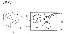
- the linear structure forms a network structure in the conductive layer as shown in FIG.
- a single fibrous conductor 6 or a collection 7 of fibrous conductors forms a contact point by overlapping to form a network structure.
- the fibrous conductor often has a straight portion and a bent portion.
- a structure called nanowire is denoted by reference numeral 8 in FIG. As shown in the figure, it is often arc-shaped.
- the acicular conductor 9 like a whisker has a linear shape.
- the linear structure forms a network structure having contacts formed by overlapping numerals 11, 12, and 13, as shown in FIG.
- the linear structure forms a network structure, the number of conductive paths in the surface direction increases, and the surface on the protective layer side of the conductive laminate can be easily adjusted to a low surface resistance value. Also, when patterning the conductive layer, the acid component in the remover travels through the network structure and selectively erodes the linear structure, making it easier for the protective layer to remain and better durability against heat. A conductive laminate having properties can be obtained.
- the network structure in the present invention is that the linear structures are in contact with each other at at least one contact, and the smallest network structure is a case where two linear structures have a certain contact. .
- the contact may be formed by any part of the linear structure, the end parts of the linear structure are in contact with each other, the terminal and the part other than the end of the linear structure are in contact, or the linear structure Portions other than the ends of the body may be in contact with each other. Moreover, the contact may be that the contact is joined or simply contacted.
- the network structure can be observed by a method described later.
- an inorganic polymer compound or an organic polymer compound is preferably used as the component of the protective layer in the present invention.
- inorganic polymer compounds include inorganic oxides.
- tetraalkoxysilanes such as tetramethoxysilane, tetraethoxysilane, tetra-n-propoxysilane, tetra-i-propoxysilane, tetra-n-butoxysilane, methyltrimethoxysilane, methyltriethoxysilane, ethyltri Methoxysilane, ethyltriethoxysilane, n-propyltrimethoxysilane, n-propyltriethoxysilane, i-propyltrimethoxysilane, i-propyltriethoxysilane, n-butyltrimethoxysilane, n-butyltriethoxysilane, n-pentyltrimethoxysilane, n-pentyltriethoxysilane, n-pent
- organic polymer compound examples include thermoplastic resins, thermosetting resins, photocurable resins, and the like, and in consideration of visible light permeability, base material heat resistance, glass transition point, film hardness, etc. You can choose.
- resins include polyester resins such as polyethylene terephthalate and polyethylene naphthalate, polycarbonate resins, acrylic resins, methacrylic resins, urethane acrylate resins, urethane methacrylate resins, epoxy resins, and polyamide resins such as nylon and benzoguanamine.
- Resins ABS resins, polyimide resins, olefin resins such as polyethylene and polypropylene, polystyrene resins, polyvinyl acetate resins, melamine resins, phenol resins, resins containing chlorine atoms such as polyvinyl chloride and polyvinylidene chloride, Fluorine atom-containing resin (for example, polyester resin, acrylic resin, methacrylic resin, epoxy resin, olefin resin such as polyethylene and polypropylene, etc.) Resin containing elemental atoms), silicone resins (linear silicone resins, silicone resin resins, linear silicone resins, copolymers of silicone resin resins and other resins, and copolymers of graft structures, Introduce various functional groups into the structure such as the terminal chain, molecular chain, and branched chain of silicone in linear silicone resin, silicone resin resin, copolymer with other resins, and copolymer of graft structure.
- silicone resins linear silicone resins, silicone resins
- Organic polymer compounds such as modified silicone resins). Further, it may be a resin obtained from a compound having a carbon-carbon double bond group that contributes to two or more polymerization reactions in the structure used for the above-mentioned crosslinked layer. Based on the application, required characteristics, productivity, and the like, a composition containing one or more of these, or an oligomer obtained by copolymerizing two or more of these can be used. It is more preferable to use a polymer compound that does not contain any of the S element, P element, metal element, metal ion, and N element constituting the functional group.
- S element, P element, and N element may have an electron pair (lone electron pair) that does not bond to other elements due to their electron orbital state, or a functional group having an ionic bond with a metal ion (for example, —ONa, -COONa, -SO 3 Na, etc.).
- the metal element may form a coordination bond.
- the durability of the protective layer against heat is reduced, or the protective layer has the above-mentioned removal agent against Resistance may be reduced. Therefore, when a polymer compound that does not contain any of these S element, P element, metal element, metal ion, and N element constituting the functional group is used, it becomes easy to increase the durability against heat and the resistance to the removing agent. It is preferable because the thickness of the protective layer can be reduced and the removal component of the removal agent can be easily changed.
- Examples of the polymer compound that does not contain any of the S element, P element, metal element, metal ion, and N element constituting the functional group include the acrylic resin, methacrylic resin, urethane acrylate resin, urethane Examples thereof include methacrylate resins, resins containing elemental fluorine (F element), silicone resins, and the like. One or more of these can be used based on the required characteristics and productivity.
- a polymer compound selected from polyfunctional urethane methacrylate polymer compounds can be preferably used.
- polyfunctional monomer and polyfunctional oligomer forming the polyfunctional acrylic polymer compound polyfunctional methacrylic polymer compound, polyfunctional urethane acrylate polymer compound, polyfunctional urethane methacrylate polymer compound, the above-mentioned cross-linked layer
- the compounds exemplified as the compounds having a carbon-carbon double bond group contributing to two or more polymerization reactions in the structure used in the above can be suitably used.
- the polymer compound constituting the protective layer has a cross-linked structure because durability against heat and resistance to a removal component of the removal agent can be further improved.
- the cross-linked structure is a state where the bonds of the components forming the protective layer are three-dimensionally connected.
- the bonding of the components constituting the protective layer becomes dense and the free volume of the protective layer is reduced.
- the effect of suppressing the migration of oligomers from the substrate and the penetration of the removed components into the protective layer It is presumed that the effect of suppressing the heat resistance increases, thereby improving the durability of the laminate to heat.
- a crosslinked structure of an organic polymer compound is preferable because flexibility and flexibility are reduced as compared with the polymer compound, the protective layer becomes brittle, and brittle fracture may easily occur during production.
- the method for converting the organic polymer compound into a crosslinked structure is shown below.
- the method shown below can be applied suitably also when laminating
- the technique include a method of heat curing using a polyfunctional monomer or polyfunctional oligomer as a raw material, and a method of photocuring by irradiation with radiation such as ultraviolet light, visible light, or electron beam.
- radiation such as ultraviolet light, visible light, or electron beam.
- thermal curing since the heat energy is the driving force of the curing reaction, if the monomers and oligomers are made more multifunctional, it may be necessary to take measures such as requiring a longer reaction time and a longer curing time.
- the photoinitiator absorbs radiation such as ultraviolet light, visible light, and electron beam, generates active species such as radical species, cation species, and anion species that are reaction initiation species, and initiates a chemical reaction. It is a substance. These may be used alone, but it is preferable to use two or more photoinitiators each having a maximum absorption wavelength value of 20 nm or more.
- the radical species is very reactive, but because of its high reactivity, the radicals are deactivated before reacting, and the formation of a crosslinked structure seems to be expected. May not progress to However, an emitter such as a lamp that emits radiation does not actually emit only a single wavelength of radiation, but emits radiation of various wavelengths. By mixing two or more photoinitiators having a difference in maximum absorption wavelength of 20 nm or more, a wider range of wavelengths can be used, and as a result, the reaction can proceed sufficiently. Furthermore, it is more effective to contain three or more photoinitiators.
- the maximum absorption wavelength here is a wavelength at which the absorption spectrum obtained by dissolving a photoinitiator in a solvent and obtained by UV-Vis spectrophotometry (UV-Vis) has a maximum value.
- UV-Vis UV-Vis spectrophotometry
- the maximum value having the highest absorbance among the plurality of maximum values is taken. If the difference in maximum absorption wavelength is less than 20 nm, there is a region where the absorption bands of the mixed photoinitiators overlap, so it is estimated that only the same effect as that of one type of photoinitiator can be obtained. Yes.
- an atmosphere substituted with an inert gas such as nitrogen or argon in order to suppress deactivation of the starting species by oxygen It is also effective to form a crosslinked structure of the protective layer under an atmosphere with a low oxygen concentration, such as under or under an oxygen-deaerated atmosphere. It is particularly preferable to form a cross-linked structure by containing two or more photoinitiators having different maximum absorption wavelength values of 20 nm or more in an atmosphere having a low oxygen concentration.
- photoinitiator examples include benzophenone photoinitiators such as benzophenone, hydroxybenzophenone and 4-phenylbenzophenone; benzoin photoinitiators such as benzyldimethyl ketal; 1-hydroxy-cyclohexyl-phenyl-ketone, 2-hydroxy-2 -Methyl-1-phenylpropan-1-one, 2-methyl 1 [4- (methylthio) phenyl] -2-morpholinopropan-1-one, 2-benzyl-2-dimethylamino-1- (4- ⁇ -hydroxyketone photoinitiators such as morpholinophenyl) -butanone and ⁇ -aminoketone photoinitiators; thioxanthone photoinitiators such as isopropylthioxanthone and 2-4-diethylthioxanthone; methylphenylglyoxylate, etc.
- benzophenone photoinitiators such as benzophenone, hydroxy
- photoinitiators include, for example, Ciba (registered trademark) IRGACURE (registered trademark) 184 (manufactured by Ciba Japan Co., Ltd.) as 1-hydroxy-cyclohexyl-phenyl-ketone, 2-methyl 1 [4- (methylthio Ciba (registered trademark) IRGACURE (registered trademark) 907 (manufactured by Ciba Japan Co., Ltd.), 2-benzyl-2-dimethylamino-1- (4-) phenyl] -2-morpholinopropan-1-one
- Examples of morpholinophenyl) -butanone-1 include Ciba (registered trademark) IRGACURE (registered trademark) 369 (manufactured by Ciba Japan Co., Ltd.).
- the static friction coefficient (hereinafter sometimes simply referred to as the static friction coefficient) between the crosslinked layer side and the protective layer side based on JIS C2151 (2006) is 0.75 or less, and JIS The dynamic friction coefficient based on C2151 (2006) (hereinafter sometimes simply referred to as the dynamic friction coefficient) is preferably 0.65 or less.
- a conductive laminate as in the present invention when laminating each layer on a substrate, unwinds the substrate wound up in a roll shape by a processing device, forms a layer on the substrate, and then rewinds the substrate. In many cases, the product is produced in a roll-to-roll form.
- the conductive laminate of the present invention is processed into an electrode member after production, processing by roll-to-roll is often employed in the same manner.
- a roll is formed in a state where the cross-linked layer side and the protective layer side of the conductive laminate are in contact with each other. Or both may be damaged.
- the portion of the scratch thus generated is a defect such as a crack in which each layer is beaten or cracked.
- the laminated thickness of the cross-linking layer and the protective layer is extremely thin at that portion, or the base material is exposed, which may be the starting point for oligomer precipitation due to heat.
- the network structure of the linear structure is destroyed and the flow of electricity is obstructed, so that the surface resistance value rises, or the scratched part can be visually recognized, resulting in a touch panel, electronic paper, etc.
- the quality of the product may be reduced.
- the static friction coefficient between the cross-linked layer side and the protective layer side is 0.75 or less and the dynamic friction coefficient is 0.65 or less.
- the conductive laminate and the product using the same can be combined with durability against heat, good conductivity, and high quality. If the static friction coefficient is greater than 0.75, the portion where the cross-linked layer and the protective layer are in contact with each other may be easily damaged at the start of operation during processing.
- the static friction coefficient is preferably 0.60 or less, and more preferably 0.55 or less.
- the dynamic friction coefficient is preferably 0.50 or less, more preferably 0.45 or less.
- the lower limit of each coefficient of friction is not particularly limited from the viewpoint of the formation of the scratches described above, but depending on the winding method and winding hardness when winding the conductive laminate on a roll, it may slip too much, making it difficult to wind or transfer. Since the roll shape is likely to collapse when the roll is tilted, a static friction coefficient of 0.08 or more and a dynamic friction coefficient of 0.05 or more are preferable.
- a method for setting the static friction coefficient and the dynamic friction coefficient in the specific range a method of mixing an additive for improving slipperiness into the cross-linked layer or the protective layer can be mentioned. Since the additive may bleed out, is it possible to react and fix the additive with the compound used when forming each layer by irradiating with radiation such as heating, ultraviolet light, visible light, or electron beam? Alternatively, it is preferable to adopt a method of selecting a compound that can form a layer satisfying each friction coefficient by the compound itself used in forming each layer. Furthermore, a method for bringing the static friction coefficient and the dynamic friction coefficient into the specific ranges may be applied to both the crosslinked layer and the protective layer. However, if the effect is manifested, it should be applied to only one of the layers.
- the linear structure which is a conductive material it is preferably applied to the crosslinked layer side.
- the additive for reducing the static friction coefficient and the dynamic friction coefficient include low molecular weight compounds / monomers / oligomers containing fluorine atoms, silicone-based low molecular weight compounds / monomers / oligomers / resins, and the like.
- monomers or oligomers such as silicone triacrylate, silicone trimethacrylate, silicone tetraacrylate, silicone tetramethacrylate, silicone pentaacrylate, silicone pentaacrylate, silicone hexaacrylate, silicone hexamethacrylate, etc., in which a silicone skeleton is introduced are used as additives.
- These additives can be fixed by reacting with the compounds used in forming each layer. Examples of such commercially available additives include EBECRYL 1360 manufactured by Daicel-Cytec Co., Ltd., X-12-2456 series manufactured by Shin-Etsu Chemical Co., Ltd., and the like.
- the conductive laminate of the present invention has a friction direction when either the cross-linked layer surface or the protective layer surface is subjected to 50 reciprocating frictions with a test white cloth cotton (Kanakin No. 3) by a method based on JIS L0849 (2004). It is preferable that the number of scratches generated in the parallel direction is 10 or less in a 2 cm square. As described above, scratches formed in the crosslinked layer and the protective layer cause deterioration in heat durability, conductivity, and quality, so the crosslinked layer or the protective layer itself is not easily damaged, that is, has high scratch resistance. A layer having scratching properties is also preferred.
- the number of scratches generated in the direction parallel to the friction direction is preferably 5 or less, more preferably 3 or less, and most preferably 0 in a 2 cm square.
- a functional group containing a carbon-carbon double bond group that contributes to the polymerization reaction among the compounds for forming a crosslinked layer or a protective layer is a molecule. Examples thereof include a method using a compound containing four or more compounds, that is, a compound having four or more functions.
- the molecular chain is fixed at that point, and it is difficult for the molecular chain to break against physical stress (in this case, 50 reciprocating friction with the attached white cloth for cotton (Kanakin No. 3)). Therefore, it is estimated that the surface scratch resistance is increased.
- examples of those that easily impart surface scratch resistance include pentaerythritol tetraacrylate, pentaerythritol tetramethacrylate, pentaerythritol ethoxytetraacrylate, pentaerythritol ethoxytetramethacrylate.
- a cyclic skeleton such as cyclopropane ring, cyclobutane ring, cyclopentane ring and cyclohexane ring in the molecular structure.
- those having other skeletons together with carbon-carbon double bond groups in the skeleton such as urethane tetraacrylate, urethane tetramethacrylate, urethane pentaacrylate, urethane pentamethacrylate, urethane hexaacrylate, urethane hexamethacrylate having a urethane skeleton; Polyether tetraacrylate, polyether tetramethacrylate, polyether pentaacrylate, polyether pentamethacrylate, polyether hexaacrylate, polyether hexamethacrylate; epoxy tetraacrylate having epoxy-derived skeleton, epoxy tetramethacrylate, epoxy pentaacrylate, epoxy Penta methacrylate, epoxy hexaacrylate, epoxy hexa Methacrylate; polyester tetraacrylate having an ester skeleton, a polyester tetramethacrylate, polyester pentaacrylate,
- the surface resistance value on the cross-linked layer side is preferably 1 ⁇ 10 13 ⁇ / ⁇ or less.
- dust and dust may adhere. This dust and dust may cause scratches and defects, which may cause deterioration in durability against heat, and may result in touch panels and electronic devices being obtained. There is a case where the quality of paper or the like is deteriorated.
- the surface resistance value on the cross-linked layer side is 1 ⁇ 10 13 ⁇ / ⁇ or less, it may cause dust or dirt even if it is not a dust-proof environment in the transport / transport process / process of the conductive laminate.
- the surface resistance value on the cross-linked layer side is preferably 1 ⁇ 10 12 ⁇ / ⁇ or less, more preferably 1 ⁇ 10 10 ⁇ / ⁇ or less.
- the surface resistance value on the cross-linked layer side is preferably 1 ⁇ 10 8 ⁇ / ⁇ or more.
- Antistatic mechanisms applicable to the present invention include (1) ionic conduction and (2) electronic conduction.
- the components of the crosslinked layer are mixed with components of cationic species, anionic species and nonionic species, or directly bonded to the components in the layer.
- the surface resistance value of the layer can be adjusted.
- the method of directly bonding to the component in the layer is preferable because the component imparting antistatic properties is less likely to bleed out or deteriorate and the initial surface resistance value can be easily maintained over a long period of time.
- Examples of commercially available components that can be used in the mixing method include, for example, Electro Stripper (registered trademark) QN, Electro Stripper (registered trademark) AC, Rheodor (registered trademark) TW-L120 manufactured by Kao Corporation, Emazol (registered trademark) L-10V, Hostastat (registered trademark) FA 14, Hostastat (registered trademark) FA 18, Hostastat (registered trademark) FA 38, Hostastat (registered trademark) FE 2, Hoststat (manufactured by Clariant Japan Co., Ltd.) (Registered trademark) FE 20, “Saftmer” (registered trademark) ST-1000 series, “Saftmer” (registered trademark) ST-2000 series, “Saftmer” (registered trademark) ST-3000 series, etc., manufactured by Mitsubishi Chemical Corporation, etc.
- Raised It is.
- Examples of commercially available components that can be used in the method of directly bonding to a part of the components contained in the cross-linked layer include Fulcure (registered trademark) HCE-022, manufactured by Soken Chemical Co., Ltd. Registered trademark) HCE-032, “LIODURAS” (registered trademark) LAS1211 manufactured by Toyo Ink Manufacturing Co., Ltd., and the like.
- the antistatic mechanism by electronic conduction of (2) is a layer to impart antistatic properties to components that conduct electricity themselves, such as metal fine particles, metal oxide fine particles, or the linear structure used in the present invention. By adding it to the surface, the surface resistance value is adjusted by the conductivity of these components.
- the linear structure that is the conductive component of the conductive layer described above may be applied as a component that conducts electricity, or antimony pentoxide, tin oxide, antimony-doped tin oxide (ATO), indium oxide, tin-doped oxidation.
- ITO Indium
- TiO Indium
- Zrconium oxide titanium oxide, zirconium oxide, barium sulfate, tin oxide, or the like doped or surface-coated with a component selected from Al, Ga, tin, phosphorus, fluorine, and ATO
- Examples of commercially available fine particle powders include, for example, Pastoran (registered trademark) TYPE-IV 4000 series, Pastoran (registered trademark) TYPE-IV 6000 series manufactured by Mitsui Mining & Smelting Co., Ltd. GK, passest AK, passest AB, 23-K and the like.
- catalyst examples include ELCOM (registered trademark) P-3501 and ELCOM (registered trademark) TO-1002ATC manufactured by Kasei Kogyo Co., Ltd.
- a conductive component is mixed with a compound that can be used in the above-mentioned crosslinked layer, for example, Fure Cure (registered trademark) LHT-11 manufactured by Soken Chemical Co., Ltd., manufactured by Toyo Ink Manufacturing Co., Ltd.
- LIODURAS (registered trademark) LASTYP series
- LIODURAS (registered trademark) LASTTYZA series
- LIODURAS (registered trademark) LASTYST series
- LIODURAS (registered trademark) LASTTYPT Series
- LIODURAS registered trademark
- the transmitted light color tone b * in the L * a * b * display color system based on JIS Z8729 (2004) when light from a C light source is incident from the cross-linked layer side is 1.5 or less.
- a touch panel or electronic paper may use a plurality of electrode members depending on its configuration and operation method.
- the display principle of the touch panel and electronic paper uses the transmitted light of the light source installed on the back of the display unit called the backlight and the reflected light of the light incident from the outside light, so when using multiple electrode members, Absorption of light by each layer of the conductive laminate or reflection of light at the interface between air and each layer may appear yellowish, which may cause deterioration in color reproducibility and image quality of displayed images.
- the transmitted light color tone b * value (C light source) is adopted as a yellowness index, and the transmitted light color tone b * value (C light source) when the light is incident from the cross-linked layer side of the conductive laminate is 1.5 or less. Even in a product including a plurality of the conductive laminates of the present invention, it is possible to prevent the color reproducibility deterioration and the image quality deterioration of the displayed image.
- the transmitted light color tone b * value (C light source) is preferably 1.0 or less, more preferably 0.5 or less. Further, the b * value (C light source) is preferably ⁇ 5.0 or more, more preferably ⁇ 4.0 or more, and further preferably ⁇ 3.0 or more.
- the b * value (C light source) of transmitted light to 1.5 or less
- it is effective to color the conductive laminate to blue, which is a complementary color of yellow, and blue-based pigments, dyes or pigments, blue
- the b * value can be lowered by adding, dispersing, compatibilizing, or bonding an additive such as a resin having a tinge.
- additives such as blue pigments, dyes, and pigments
- additives include, for example, a compound having an anthraquinone skeleton, a compound having a porphyrin skeleton, a compound having a tetraazaporphyrin skeleton, a compound having a phthalocyanine skeleton, Pigment Blue 15, 15: 3, 15: 4, 15: 6, 22, 60, 64; compounds disclosed in Japanese Patent No. 3879402 and Japanese Patent No. 4440720.
- Examples of commercially available products include, for example, Kayset (registered trademark) Blue FR, Kayase (registered trademark) Blue N, Kayase (registered trademark) Blue A-2R of Kayset (registered trademark) series manufactured by Nippon Kayaku Co., Ltd. , Kayset (registered trademark) Blue AD, and Kayase (registered trademark) Blue A-CR.
- a layer colored with these blue additives any of a base material, a crosslinked layer, a conductive layer, and a protective layer may be used, but the influence on the linear structure as a conductive material, productivity, etc. are considered. It is preferable to color the crosslinked layer.
- the preferred content of the blue-based additive varies depending on the type of additive and the thickness of the layer to be added, but the blue-based addition to the total solid content of the layer to be added (T) ( ⁇ m) and the layer to be added
- the product (T) ⁇ (A) with the mass content (A) (% by mass) of the agent is preferably 0.10 or more and 0.50 or less, more preferably 0.15 or more and 0.30 or less. is there.
- the conductive laminate of the present invention preferably has a total light transmittance of 80% or more based on JIS K7361-1 (1997) when light is incident from the conductive layer side. This is because a touch panel incorporating a conductive laminate having a total light transmittance of 80% or more exhibits excellent transparency and can clearly recognize the display on a display provided in the lower layer of the touch panel.
- the total light transmittance is preferably 85% or more, more preferably 90% or more.
- a method for increasing the total light transmittance for example, a method for increasing the total light transmittance of a substrate to be used, a method for reducing the thickness of the conductive layer, and a protective layer as an optical interference film. And the like, and the amount of the blue-based additive added as much as possible.
- a method for increasing the total light transmittance of the base material a method of reducing the thickness of the base material or a method of selecting a base material made of a material having a large total light transmittance can be mentioned.
- the material having a large total light transmittance include a highly transparent resin and glass. Even if it is a film that can be wound up with a thickness of 250 ⁇ m or less, or a substrate with a thickness of more than 250 ⁇ m, it can be preferably used as long as it is within the above-mentioned total light transmittance.
- a resin film having a thickness of 250 ⁇ m or less is preferable, more preferably 190 ⁇ m or less, still more preferably 150 nm or less, and most preferably 100 ⁇ m or less.
- the thickness of the base material is 100 ⁇ m or less, the touch panel and electronic paper using a plurality of conductive laminates as electrode members can be reduced in weight and thickness, the optical characteristics can be improved, The thinness can reduce the thermal processing temperature or shorten the thermal processing time, which may suppress oligomer precipitation during processing, and is a cost and performance advantage when making products such as touch panels and electronic paper. Is big.
- polyesters such as polyethylene terephthalate (PET) and polyethylene naphthalate (PEN), polyimide, polyphenylene sulfide, aramid, polypropylene, polyethylene, polylactic acid, polyvinyl chloride, polycarbonate, polymethacrylic acid Examples thereof include methyl, alicyclic acrylic resin, cycloolefin resin, triacetyl cellulose, and those obtained by mixing or copolymerizing these resins.
- the substrate for example, an unstretched film, a uniaxially stretched film, or a biaxially stretched film made of these resins can be applied.
- polyester films such as polyethylene terephthalate (PET) films and polyethylene naphthalate (PEN) films, and PEN are mixed and / or copolymerized.
- PET polyethylene terephthalate
- PEN polyethylene naphthalate
- As the material of the glass substrate ordinary soda glass can be used.
- a combination of these materials can be used.
- a composite substrate such as a substrate in which a resin and glass are combined and a substrate in which two or more kinds of resins are laminated may be used.
- the base material may be surface-treated as necessary.
- the surface treatment may be a glow discharge treatment, a corona discharge treatment, a plasma treatment, a flame treatment or the like, or a resin layer.
- a film having an easy-adhesion layer on the surface can also be preferably used as the substrate.
- the kind of base material is not limited to the above, and an optimal one can be selected from transparency, durability, flexibility, cost, etc. according to the application.
- the protective layer becomes an optical interference film.
- the conductive layer reflects or absorbs light depending on the physical properties of the conductive component. Therefore, in order to increase the total light transmittance of the conductive laminate, the protective layer is designed to be an optical interference film, and the average reflectance of light with a wavelength of 380 to 780 nm on the protective layer side is lowered to 4% or less. It is effective.
- the average reflectance of light having a wavelength of 380 to 780 nm on the protective layer side is preferably 3% or less, more preferably 2% or less. When the average reflectance is 4% or less, a performance with a total light transmittance of 80% or more when used for touch panel applications can be obtained with good productivity.
- the surface resistance value on the conductive layer side is preferably 1 ⁇ 10 0 ⁇ / ⁇ or more and 1 ⁇ 10 4 ⁇ / ⁇ or less, more preferably 1 ⁇ 10 1 ⁇ / ⁇ .
- the above is 1.5 ⁇ 10 3 or less.
- it can be preferably used as a conductive laminate for a touch panel. That is, when the surface resistance value is 1 ⁇ 10 0 ⁇ / ⁇ or more, power consumption can be reduced. Moreover, when the surface resistance value is 1 ⁇ 10 4 ⁇ / ⁇ or less, the influence of errors in the coordinate reading of the touch panel can be reduced.
- additives can be added to the substrate and each of the above layers within a range that does not impair the effects of the present invention.
- additives include organic and / or inorganic fine particles, crosslinking agents, flame retardants, flame retardant aids, heat stabilizers, oxidation stabilizers, leveling agents, slip activators, conductive agents, antistatic agents, and ultraviolet rays.
- Absorbers, light stabilizers, nucleating agents, dyes, fillers, dispersants, coupling agents, and the like can be used.
- a method for producing the conductive laminate of the present invention will be described with an example.
- a cross-linked layer is formed on one side of the base material, a conductive layer is formed on the other side of the base material, and a protective layer is formed on the conductive layer. It is preferable to do.
- an optimal method may be selected depending on the material to be formed. Dry methods such as vacuum deposition, EB deposition, and sputtering, casting, spin coating, dip coating, and bar coating And general methods such as spray coating, blade coating, slit die coating, gravure coating, reverse coating, screen printing, mold coating, printing transfer, and wet coating methods such as inkjet. Of these, a slit die coat that can uniformly coat the protective layer and hardly damage the lower layer, or a wet coat method using a micro gravure that can form the protective layer uniformly and with high productivity is preferable.
- a removing agent is applied on the protective layer in a portion where the conductive layer of the conductive laminate is to be removed.
- the remover has non-Newtonian fluidity, it can be applied using a known method regardless of the type, size, and shape of the conductive laminate, which is preferable.
- the coating method include screen printing method, dispenser method, stencil printing method, pad printing method, spray coating, ink jet method, micro gravure printing method, knife coating method, spin coating method, slit coating method, roll coating method, curtain Examples thereof include, but are not limited to, a coating method and a flow coating method. In order to further reduce the etching unevenness of the conductive layer, it is preferable to apply the removing agent uniformly.
- the thickness of the removal film formed by applying the removing agent is appropriately determined depending on the material and thickness of the conductive layer to be removed, the heating temperature and the heating time.
- the thickness after drying is preferably from 0.1 to 200 ⁇ m, more preferably from 2 to 200 ⁇ m.
- the conductive laminate coated with the removing agent is heat-treated at 80 ° C. or higher.
- the heat treatment temperature is preferably lower than the boiling point of components other than the solvent contained in the removal agent, and is preferably 200 ° C. or lower.
- the heat treatment means can be selected according to the purpose and application, and examples thereof include, but are not limited to, a hot plate, a hot air oven, an infrared oven, and microwave irradiation with a frequency of 300 megahertz to 3 terahertz.
- the removal agent and the dissolved or decomposed material of the conductive layer and the protective layer are removed by washing with a liquid to obtain a desired conductive pattern.
- the liquid used in the washing step is preferably one in which the resin contained in the removal agent dissolves, and specifically, ketones such as acetone, alcohols such as methanol, and organic solvents such as tetrahydrofuran are raised.
- the aqueous solution containing the said organic solvent, the basic aqueous solution containing sodium hydroxide, ethanolamine, a triethylamine, a pure water, etc. are mentioned, However It is not limited to these.
- the liquid may be heated to 25 to 100 ° C. and used.
- a remover is a solution containing an acid component or a base component.
- the linear structure of the conductive layer can be selectively removed by applying a removing agent on the protective layer.
- the acid component or the base component is preferably one or more selected from the group consisting of acids having a boiling point of 80 ° C. or higher, bases having a boiling point of 80 ° C. or higher, or compounds that generate an acid or a base by external energy.
- the remover preferably contains an acid component or a base component, a solvent, a resin, and a leveling agent.
- the removal agent is applied to a part of the protective layer on the conductive layer side, heat-treated at 80 ° C. or higher, and then washed with a liquid to selectively remove the conductive layer in the portion where the removal agent is applied. Can be removed.
- the heat treatment temperature is preferably lower than the boiling point of components other than the solvent in the removing agent, and is preferably 200 ° C. or lower.
- the boiling point is a value under atmospheric pressure, and is measured according to JIS-K5601-2-3 (1999).
- the boiling point of the acid used for the remover is preferably 100 ° C. or higher, and more preferably 200 ° C. or higher.
- an acid that does not have a clear boiling point under atmospheric pressure and starts thermal decomposition prior to vaporization when the temperature is raised is 80 ° C. or higher if the temperature at which thermal decomposition starts is 80 ° C. or higher.
- the thing whose vapor pressure in the heat processing temperature at the time of removing a conductive layer is 30 kPa or less is more preferable. Examples of the acid having a boiling point of 80 ° C.
- monocarboxylic acids such as formic acid, acetic acid, and propionic acid; dicarboxylic acids such as oxalic acid, succinic acid, tartaric acid, and malonic acid; tricarboxylic acids such as citric acid and tricarballylic acid; Alkylsulfonic acid such as methanesulfonic acid; phenylsulfonic acid such as benzenesulfonic acid; alkylbenzenesulfonic acid such as toluenesulfonic acid and dodecylbenzenesulfonic acid; phenolsulfonic acid; nitrobenzenesulfonic acid; styrenesulfonic acid; sulfone such as polystyrenesulfonic acid Acid compounds; derivatives obtained by partially fluorinating organic acids such as trifluoroacetic acid; inorganic acids such as sulfuric acid, hydrochloric acid, nitric acid and phosphoric acid. Two or more
- acids having high oxidizing power are preferable, and sulfuric acid or sulfonic acid compounds are more preferable.
- the boiling point of sulfuric acid under atmospheric pressure is 290 ° C., for example, the vapor pressure of sulfuric acid at 150 ° C. is 1.3 kPa or less, the liquid state is maintained even when heated at this temperature, and the linear structure in the conductive layer Penetrates deeply.
- sulfuric acid since sulfuric acid has a high oxidizing power, it reacts easily with the conductive layer even at a low temperature of about 80 to 200 ° C., and can be conducted without affecting the substrate by heat treatment in a shorter time than nitric acid or acetic acid. The layer can be removed.
- the sulfonic acid compound is a solid acid under atmospheric pressure, it does not evaporate.
- the vapor pressure at 150 ° C. is 1.3 kPa or less, it evaporates or sublimes even when heated at this temperature. Since the reaction is efficiently promoted during heating, the conductive layer can be removed by a short heat treatment.
- the removal agent containing a solid acid can easily control non-Newtonian fluidity, for example, a linear pattern with a small line width of about 30 ⁇ m can be formed with less variation (swell) in the line width. A pattern can be formed, which is particularly preferable.
- the boiling point of the base used for the removing agent is preferably 100 ° C. or higher, and more preferably 150 ° C. or higher.
- Bases that do not have a clear boiling point under atmospheric pressure and that start thermal decomposition prior to vaporization when the temperature rises are included in bases that have a boiling point of 80 ° C. or higher if the temperature at which thermal decomposition starts is 80 ° C. or higher.
- the thing whose vapor pressure in the heat processing temperature at the time of removing an electrically conductive film is 30 kPa or less is more preferable. Examples of the base having a boiling point of 80 ° C.
- Examples of the compound that generates acid by external energy include compounds that generate acid by irradiation with radiation such as ultraviolet rays and / or heat.
- radiation such as ultraviolet rays and / or heat.
- 4-hydroxyphenyldimethylsulfonium, sulfonium compounds such as hexafluoroantimonate and trifluoromethanesulfonate
- benzophenone compounds such as 4,4-bis (dimethylamine) benzophenone and 4,4-dichlorobenzophenone
- benzoins such as benzoin methyl ether Compounds
- phenyl ketone compounds such as 4-benzoyl-4-methyldiphenyl ketone and dibenzyl ketone
- acetophenone compounds such as 2,2-diethoxyacetophenone and 2-hydroxy-2-methylpropionphenone
- 2,4-diethylthioxanthene Thioxanthene compounds such as -9-one and 2-chlorothioxanthone
- Examples of the compound that generates a base by external energy include a compound that generates a base by irradiation with radiation such as ultraviolet rays and / or heat.
- a compound that generates a base by irradiation with radiation such as ultraviolet rays and / or heat.
- radiation such as ultraviolet rays and / or heat.
- the content of the acid component or the base component is preferably 1 to 80% by mass in the components excluding the solvent.
- the content of the acid having a boiling point of 80 ° C. or more is preferably 10 to 70% by mass, more preferably 20 to 70% by mass in the component excluding the solvent.
- the content of the base having a boiling point of 80 ° C. or higher is preferably 0.01 to 70% by mass in the components excluding the solvent.
- the content of the compound that generates an acid by external energy is preferably 0.1 to 70% by mass in the components excluding the solvent.
- the content of the compound that generates a base by external energy is preferably 1 to 80% by mass in the components excluding the solvent. However, it is not limited to this range, and can be appropriately selected depending on the molecular weight of the compound, the amount of acid or base generated, the material and film thickness of the conductive layer to be removed, the heating temperature and the heating time.
- the solvent used for the remover include acetates such as ethyl acetate and butyl acetate; ketones such as acetone, acetophenone, ethyl methyl ketone and methyl isobutyl ketone; aromatic hydrocarbons such as toluene, xylene and benzyl alcohol Alcohols such as methanol, ethanol, 1,2-propanediol, terpineol, acetyl terpineol, butyl carbitol, ethyl cellosolve, ethylene glycol, triethylene glycol, tetraethylene glycol, glycerol; triethylene glycol monobutyl ether, etc.
- acetates such as ethyl acetate and butyl acetate
- ketones such as acetone, acetophenone, ethyl methyl ketone and methyl isobutyl ketone
- aromatic hydrocarbons such as tolu
- Ethylene glycol monoalkyl ethers ethylene glycol dialkyl ethers; diethylene glycol monoalkyl ether acetates; ethylene glycol monoary Polyethylene glycol monoaryl ethers; propylene glycol monoalkyl ethers; dipropylene glycol dialkyl ethers; propylene glycol monoalkyl ether acetates; ethylene carbonate, propylene carbonate, ⁇ -butyrolactone, solvent naphtha, water, N-methyl
- Examples include pyrrolidone, dimethyl sulfoxide, hexamethylphosphoric triamide, dimethylethylene urea, N, N′-dimethylpropylene urea, and tetramethyl urea. Two or more of these may be mixed and used.
- the content of the solvent in the removing agent is preferably 1% by mass or more, more preferably 30% by mass or more, and further preferably 50% by mass or more.
- the content of the solvent is preferably 99.9% by mass or less, and more preferably 95% by mass or less.
- the removal agent preferably contains a resin.
- a resin By containing the resin, non-Newtonian fluidity can be imparted to the remover, and it can be easily applied to the conductive laminate by a known method. Moreover, the flow of the removal agent at the time of heat processing can be suppressed, and the precision of an application position can be improved.
- the resin that can be used for this purpose include polystyrene resin, polyacrylic resin, polyamide resin, polyimide resin, polymethacrylic resin, melamine resin, urethane resin, benzoguanamine resin, phenol resin, silicone resin, and fluorine resin. it can. Two or more of these may be contained.
- hydrophilic resin such as a nonionic hydrophilic resin, an anionic hydrophilic resin, an amphoteric hydrophilic resin, or a cationic hydrophilic resin
- it can be easily washed with water, an aqueous basic solution, or an organic solvent aqueous solution. It is possible to reduce the residue on the removal surface.
- hydrophilic resins include polyvinyl pyrrolidone, hydrophilic polyurethane, polyvinyl alcohol, polyethyloxazoline, polyacrylic acid, gelatin, hydroxyalkyl guar, guar gum, locust bean gum, carrageenan, alginic acid, gum arabic, and pectin.
- Xanthan gum cellulose, ethylcellulose, hydroxypropylcellulose, carboxymethylcellulose, sodium carboxymethylhydroxyethylcellulose, acrylamide copolymer, polyethyleneimine, polyaminesulfonium, polyvinylpyridine, polydialkylaminoethyl methacrylate, polydialkylaminoethyl acrylate, poly Dialkylaminoethyl methacrylamide, polydialkylaminoethyl acetate Ruamido, polyepoxy amine, polyamidoamine, dicyandiamide - formalin condensate, polydimethyl diallyl ammonium chloride, polyamine polyamide epichlorohydrin, polyvinyl amine, polyacryl amine, etc.
- a cationic resin that is not easily denatured even in the presence of an acid or under a high temperature condition and exhibits high solubility in a polar solvent is more preferable. Since the cationic resin has high solubility, the conductive layer can be removed in a short time in the step of removing the conductive layer by washing with a liquid after the heat treatment.
- cationic resin examples include polydialkylaminoethyl methacrylate, polydialkylaminoethyl acrylate, polydialkylaminoethyl methacrylamide, polydialkylaminoethyl acrylamide, polyepoxyamine, polyamidoamine, dicyandiamide-formalin condensate, polydimethyl Diallylammonium chloride, guar hydroxypropyltrimonium chloride, polyamine polyamide epichlorohydrin, polyvinylamine, polyallylamine, polyacrylamine, polyquaternium-4, polyquaternium-6, polyquaternium-7, polyquaternium-9, polyquaternium-10, polyquaternium-11, polyquaternium -16, Polyquaternium-28, Polyquaternium- 2, polyquaternium-37, polyquaternium -39, polyquaternium -51, polyquaternium -52, polyquaternium -44, polyquaternium -46, polyquaternium -
- polyquaternium-10 since polyquaternium-10 has a trimethylammonium group at the end of the side chain, the trimethylammonium group is cationized under acidic conditions, exhibits high solubility due to the action of electrostatic repulsion, and dehydration polycondensation occurs due to heating. Difficult to maintain high solvent solubility even after heating. For this reason, after the heat treatment, the conductive film can be removed in a short time in the step of removing the conductive layer by washing with a liquid, which is preferable.
- the resin content is preferably 0.01 to 80% by mass in the components excluding the solvent.
- the resin content in the remover should be as small as possible within a range that can maintain non-Newtonian fluidity, because the heating temperature required to remove the conductive layer can be kept low and the heating time can be shortened. Is more preferable.
- the viscosity of the removing agent is preferably about 2 to 500 Pa ⁇ S at 25 ° C. By setting the viscosity within such a range, a uniform coating film can be easily formed by a screen printing method.
- the viscosity of the remover can be adjusted by, for example, the contents of the solvent and the resin.
- the leveling agent used for the removing agent is preferably a compound having a property of reducing the surface tension of the removing agent to less than 50 mN / m.
- any compound having a property of reducing the surface tension to less than 50 mN / m is classified as a leveling agent even if it is a polymer compound.
- Specific examples of leveling agents include acrylic compounds such as modified polyacrylates and acrylic resins; vinyl compounds and vinyl resins having a double bond in the molecular skeleton; alkyloxysilyl groups and / or polysiloxane skeletons, etc.
- silicone compounds and silicone resins examples thereof include silicone compounds and silicone resins; fluorine compounds and fluorine resins having a fluorinated alkyl group and / or a fluorinated phenyl group. These can be appropriately selected and used depending on the material and polarity of the surface of the protective layer.
- a fluorine-based compound or a fluorine-based resin having a fluorinated alkyl group and / or a fluorinated phenyl group is particularly preferably used because of its strong ability to reduce surface tension.
- the leveling agent content is 0.001 to 0.001 in the components excluding the solvent from the balance between the surface active ability such as wettability and leveling property to the conductive laminate and the acid content of the resulting coating film. 10 mass% is preferable, 0.01 to 5 mass% is more preferable, and 0.05 to 3 mass% is more preferable.
- the removing agent When the removing agent contains an acid having a boiling point of 80 ° C. or higher or a compound that generates an acid by external energy, it preferably further contains nitrate or nitrite.
- the reaction rate between the acid and the conductive component may vary depending on the type, but by including nitrate or nitrite, the acid reacts with nitrate or nitrite during the heat treatment, and nitric acid in the system reacts. Therefore, dissolution of the conductive component can be further promoted. For this reason, the conductive layer can be removed by a short heat treatment.
- nitrate examples include lithium nitrate, sodium nitrate, potassium nitrate, calcium nitrate, ammonium nitrate, magnesium nitrate, barium nitrate, and hydrates of these nitrates.
- nitrite examples include sodium nitrite, potassium nitrite, calcium nitrite, silver nitrite, and barium nitrite. Two or more of these may be contained. Among these, in consideration of the reaction rate of nitric acid production, nitrate is preferable, and sodium nitrate or potassium nitrate is more preferable.
- the removing agent is inorganic fine particles such as titanium oxide, alumina, silica, etc .; thixotropic agent capable of imparting thixotropic properties; antistatic agent, antifoaming agent, viscosity modifier, light stabilizer, weathering agent , Additives such as heat-resistant agents, antioxidants, rust inhibitors, slip agents, waxes, mold release agents, compatibilizers, dispersants, dispersion stabilizers, rheology control agents, and the like.
- An example is given and demonstrated about the manufacturing method of a removal agent.
- the resin is added to the solvent and dissolved with sufficient stirring.
- a compound selected from an acid having a boiling point of 80 ° C. or higher, a base having a boiling point of 80 ° C. or higher, and a compound capable of generating an acid or a base by external energy, a leveling agent and, if necessary, the additive are added and stirred.
- the addition method and the addition order are not particularly limited. Stirring in each stage may be performed under heating conditions, and it is preferable to stir at 50 to 80 ° C. for the purpose of increasing the dissolution rate.
- the touch panel according to the present invention includes a single or a plurality of the conductive laminates according to the present invention, and may be mounted in combination with other members.
- Examples of the touch panel include a resistive touch panel and a capacitive touch panel.
- the touch panel of the present invention is formed by bonding and laminating a plurality of conductive laminates 14 each having a conductive layer patterned by a bonding layer 19 such as an adhesive or an adhesive.
- the base material 20 on the screen side of the touch panel and the hard coat layer 21 laminated on the surface of the base material 20 are laminated on one side of the laminate.
- Such a touch panel is used, for example, by attaching a lead wire and a drive unit, etc., and incorporating it on the front surface of the liquid crystal display.
- a ring type probe (URS probe MCP-HTP14, manufactured by Mitsubishi Chemical Corporation) is connected to form a double ring system.
- the central part of a 100 mm ⁇ 100 mm sample was measured.
- five samples were measured, and the average value was defined as a surface resistance value R 0 [ ⁇ / ⁇ ].
- each substance was concentrated and diluted as necessary to prepare samples.
- a qualitative analysis was performed to identify components contained in the sample.
- the analysis method was first performed by combining the analysis methods of the group (i), and the components that could not be detected by the analysis were analyzed by combining the analysis method of the group (ii).
- the measurement method of each group was applied in order from the one shown above, and the following measurement method was used when detection was not possible with the previous one.
- the above-mentioned ones were also used preferentially, and those that can be measured with fewer combinations were preferentially applied.
- XRD X-ray diffraction
- ND neutron diffraction
- LEED low-energy electron diffraction
- RHEED fast reflection electron diffraction
- AAS ultraviolet photoelectron spectroscopy
- UPS ultraviolet photoelectron spectroscopy
- AES Auger electron spectroscopy
- XPS X-ray photoelectron spectroscopy
- XRF X-ray fluorescence elemental analysis
- ICP-AES inductively coupled plasma emission spectroscopy
- EPMA electron microanalysis
- PIXE Charged particle excitation X-ray spectroscopy
- RBS or LEIS low energy ion scattering spectroscopy
- MEIS medium energy ion scattering spectroscopy
- ISS or HEIS high energy ion scattering spectroscopy
- GPC gel permeation chromatography
- TEM-EDX scanning electron microscope-energy dispersive X-ray Light Analysis
- TBE 1,1,2,2-tetrabromoethane
- the peak area of the peak derived from hydrogen (proton, H) of the carbon-carbon double bond group part of the functional group including the carbon-carbon double bond group, and added as an internal standard The amount of carbon-carbon double bond groups was calculated from the area ratio of the TBE to the peak area corresponding to hydrogen (proton, H), the mass of the sample measured in advance, and the concentration of the TBE internal standard solution. From this and comparison with other structures in the measurement sample calculated in the same manner, the mass content of the unit structure portion of the carbon-carbon double bond group relative to the total mass of the measurement sample was calculated.
- the carbon-carbon double bond group includes a group derived from a carbon-carbon double bond group that has been changed to another structure by reaction.
- the cantilever is a silicon single crystal
- the scanning mode is a tapping mode
- the measurement environment is a temperature of 25 ° C. and relative humidity Observation was made at 65% RH.
- each of the five points is measured (calculated from the magnification) and protected on average. The average thickness of the layer was determined. In this measurement, a magnification that can secure 3 significant digits is selected, and the value is calculated by rounding off the 4th digit.
- haze Hz after heating Five samples after heating were subjected to light incidence from the conductive layer side (protective layer side) and the haze value was measured in the same manner as before heating. An average value was calculated from the values measured for 5 samples, and this was defined as haze Hz after heating. As the haze change before and after heating, the ratio Hz / Hz 0 Initial haze Hz 0 and after heating haze Hz is evaluated as acceptable if it is 1.20 or less, Hz / Hz 0 is unacceptable to greater than 1.20 It was. Incidentally, the higher the resistance to Hz / higher Hz 0 is smaller less heat deposition of the oligomer. The most durable one has no haze change before and after heating, that is, Hz / Hz 0 is 1.0. Conversely, the greater the Hz / Hz 0, the worse the durability against heat.
- a conductive laminate in which a conductive layer was patterned was obtained as follows. A remover described later was prepared, and the remover was screen printed using a SUS # 500 mesh on the conductive laminate so that the film thickness after drying was 2.4 ⁇ m. The print pattern was a straight line having a line length of 5 cm and a line width of 500 ⁇ m. After applying the remover, put it in an infrared oven, heat-treat at 130 ° C. for 3 minutes, take it out from the oven, let it cool to room temperature, wash it with pure water at 25 ° C. for 1 minute, and remove the attached remover And the degradation product was removed.
- the substrate was drained using compressed air and then dried in an infrared oven at 80 ° C. for 1 minute to obtain a conductive laminate in which the conductive layer was patterned.
- the patterned conductive laminate was heated at 130 ° C. for 30 minutes in a thermostatic safety oven (SPHH-201 manufactured by Espec Corp.).
- SPHH-201 thermostatic safety oven
- the surface of the patterning portion was observed with an optical microscope (ECLIPSE-L200, manufactured by Nikon Corporation), and the presence or absence of oligomer precipitation on the surface of the patterning portion was observed before and after heating.
- the presence or absence of oligomer precipitation was determined by whether or not spots or spot patterns that did not exist on the surface before heating were present after heating.
- the surface was observed in the same manner using a scanning electron microscope ABT-32 manufactured by Topcon Corporation to confirm the presence or absence of oligomer precipitation. The observation is performed at an arbitrary 10 points, and the case where there is no oligomer precipitation is regarded as acceptable.
- this solution was put in a quartz cell, and an absorption spectrum at a wavelength of 200 to 900 nm at an optical path length of 1 cm using an ultraviolet-visible spectrophotometer (UV-Bis Spectrophotometer, model V-660 manufactured by JASCO Corporation). Were measured to determine the maximum absorption wavelength.
- UV-Bis Spectrophotometer model V-660 manufactured by JASCO Corporation.
- the absorption spectrum was measured three times in the same manner, and the maximum absorption wavelength was determined.
- the difference of the maximum absorption wavelength was calculated
- the maximum absorption wavelengths when there are a plurality of maximum absorption wavelengths, the following are the maximum absorption wavelengths.
- the wavelength at the maximum value with the highest absorbance was taken as the maximum absorption wavelength.
- the concentration of the photoinitiator when dissolved in the solvent is too high, the absorbance will exceed the detection limit of the device used at the maximum value with the highest absorbance, and it will be observed as if there is no such maximum value.
- the concentration of the photoinitiator was appropriately changed and the same measurement was performed, and the wavelength at the maximum value having the highest absorbance at each concentration was taken as the maximum absorption wavelength.
- Evaluation was performed using 5 samples, and the average of a total of 10 locations was calculated by rounding off the first decimal place to an integer, and the number of scratches (hereinafter simply referred to as the number of scratches) in the direction parallel to the friction direction.
- the judgment criteria in the present invention were classified into the following three stages, and the grades A and B were judged as acceptable.
- Class A The number of scratches is 2 or less.
- Class B The number of scratches is 3 or more and 10 or less.
- Class C The number of scratches is 11 or more.
- Protective layer material A A straight-chain methacrylic resin that does not contain any of the S element, P element, metal element, metal ion, and N element constituting the functional group and does not form a crosslinked structure (Foret GS-1000, manufactured by Soken Chemical Co., Ltd.) Solid content concentration 30% by mass)
- Protective layer material C A polyfunctional acrylic composition that does not contain any of the S element, P element, metal element, metal ion, and N element constituting the functional group, contains fluorine, and forms a cross-linked structure with a photoinitiator (Soken) Fur
- Protective layer material E -Polyfunctional urethane acrylate that does not contain any of the S element, P element, metal element, metal ion, and N element constituting the functional group, contains the N element in the skeletal structure, and forms a crosslinked structure with a photoinitiator Composition (Negami Kogyo Co., Ltd.
- Protective layer material F A polyfunctional acrylic / methacrylate mixed composition containing N element that forms a functional group and forming a cross-linked structure with a photoinitiator (Flucure HCE-022, manufactured by Soken Chemical Co., Ltd., solid content concentration 52.1 mass) %) (7) Protective layer material G Acrylamide t-Butyl Sulphonic Acid (also known as 2-Acrylamide-2-Methyl Propane Sulphonic Acid, 2-acrylamido-2-methylpropanesulfonic acid) and Methyl Methacrylate (also known as methyl methacrylate, 2-methyl-2-propenoic acid) Abbreviated MMA), a linear acrylic resin containing S element and not forming a cross-linked structure (solid content concentration: 100% by mass) (8) Protective layer material H ⁇ Acrylamide t-Butyl Sulfonic Acid Sodium Sait (also known as 2-Acrylamide-2-Methy
- Conductive layer A “Acicular silicon dioxide-based / ATO (antimony-doped tin oxide) composite compound conductive layer”
- this mixed solution was diluted by adding ethyl acetate so that the solid content concentration of the coating solution was 50% by mass to obtain a needle-like silicon dioxide-based / ATO composite compound-dispersed coating solution.
- This needle-like silicon dioxide-based / ATO composite compound dispersion coating liquid was applied onto a substrate using a slit die coat equipped with a SUS shim (shim thickness: 100 ⁇ m), and then dried at 120 ° C. for 5 minutes. An acicular silicon dioxide-based / ATO composite compound conductive layer was formed.
- Silver nanowires (short axis: 50 to 100 nm, long axis: 20 to 40 ⁇ m) were obtained by the method described in Example 1 (synthesis of silver nanowire) of JP-T-2009-505358.
- a silver nanowire-dispersed coating solution was obtained by the method described in Example 8 (nanowire dispersion) of JP-T-2009-505358.
- the concentration of the silver nanowire-dispersed coating liquid was adjusted so that the amount of silver nanowires relative to the entire coating liquid was 0.04% by mass.
- This silver nanowire-dispersed coating liquid whose concentration has been adjusted is applied onto a substrate using a slit die coat with a SUS shim (shim thickness: 50 ⁇ m), and then dried at 120 ° C. for 2 minutes. A conductive layer was formed.
- Conductive layer C “CNT conductive layer” (Catalyst preparation) 2.459 g of ammonium iron citrate (green) (manufactured by Wako Pure Chemical Industries, Ltd.) was dissolved in 500 mL of methanol (manufactured by Kanto Chemical Co., Inc.). To this solution, 100 g of light magnesia (Iwatani Chemical Industry Co., Ltd.) was added, stirred at room temperature for 60 minutes, dried under reduced pressure with stirring at 40 ° C. to 60 ° C. to remove methanol, and the metal salt was added to the light magnesia powder. Was obtained.
- the reactor 100 is a cylindrical quartz tube having an inner diameter of 32 mm and a length of 1200 mm.
- the reactor 100 includes a quartz sintered plate 101 at the center, an inert gas and raw material gas supply line 104 at the lower part, and an exhaust gas line 105 and a catalyst charging line 103 at the upper part.
- a heater 106 is provided that surrounds the circumference of the reactor so that the reactor can be maintained at an arbitrary temperature.
- the heater 106 is provided with an inspection port 107 so that the flow state in the apparatus can be confirmed.
- the catalyst (12 g) was taken out and charged from the sealed catalyst feeder 102 through the catalyst charging line 103, and the catalyst 108 was set on the quartz sintered plate 101. Subsequently, supply of argon gas from the source gas supply line 104 was started at 1000 mL / min. After the inside of the reactor was placed in an argon gas atmosphere, the temperature was heated to 850 ° C.
- the argon flow rate of the raw material gas supply line 104 was increased to 2000 mL / min, and fluidization of the catalyst 108 on the quartz sintered plate was started.
- methane was mixed with argon supplied from the source gas supply line 104 so that the flow rate would be 95 mL / min.
- the flow was switched to a flow of only argon gas, and the synthesis was terminated.
- the CNT composition containing the catalyst and CNTs was taken out from the reactor.
- CNT dispersion coating liquid Weigh 10 mg of CNT composition after nitric acid treatment in a 50 mL container and 10 mg of sodium carboxymethyl cellulose (Sigma, 90 kDa, 50-200 cps) as a dispersant, add distilled water to make a total amount of 10 g, Dispersion treatment was carried out under ice-cooling with an ultrasonic homogenizer output of 20 W for 20 minutes. The obtained liquid was centrifuged at 10,000 G for 15 minutes with a high-speed centrifuge, and 9 mL of the supernatant was collected.
- sodium carboxymethyl cellulose Sigma, 90 kDa, 50-200 cps
- CNT conductive layer (Formation of CNT conductive layer)
- the CNT-dispersed coating liquid was applied on a substrate using a micro gravure coater (gravure wire number 150R, gravure rotation ratio 80%), and then dried at 100 ° C. for 1 minute, and a CNT conductive layer (CNT in a CNT coating film)
- a short axis: 10 to 30 nm and a long axis: 1 to 5 ⁇ m) were formed as an aggregate.
- Conductive layer D “Silver nanoparticle conductive layer” Dispersion liquid of silver nanoparticles (short axis, long axis (particle size): 9 to 15 nm) by the method described in Examples ((2) Preparation of silver nanocolloid coating solution) in JP-A-2001-243841 Got. Next, a silver nanoparticle dispersion was applied by the method described in [Examples 1 to 8] of JP-A-2001-243841 to form a silver nanoparticle conductive layer.
- Crosslinked layer material A Polystyrene resin having a styryl group as a carbon-carbon double bond group (Styrene, Polymer (styrene, polymer) manufactured by Wako Pure Chemical Industries, Ltd.), solid content concentration: 100% by mass, cross-linking unit structure mass content: 23% by mass )
- Crosslinked layer material C An acrylic composition having an acryloyl group as a carbon-carbon double bond group (EXP8002 UV anchor agent-B manufactured by Matsuikagaku Co., Ltd., solid content concentration: 40 mass%, crosslink unit structure mass content: 12 mass%)
- Crosslinked layer material D A methacrylic composition having a methacryloyrene resin having a meth
- Crosslinked layer material F A urethane acrylate composition having an acryloyl group as a carbon-carbon double bond group (AT-600 manufactured by Kyoeisha Chemical Co., Ltd., solid content concentration: 100 mass%, cross-linking unit structure mass content: 9 mass%).
- Ciba (registered trademark)) IRGACURE (registered trademark) 369) 2.07 parts by mass (e) 0.22 parts by mass of an anthraquinone blue pigment additive (Kayaset Blue A-2R manufactured by Nippon Kayaku Co., Ltd.).
- A) Acrylic composition (Full Cure HC-6, Soken Chemical Co., Ltd., solid concentration 51% by mass) 77.80 parts by mass
- Additive B Ciba Japan Co., Ltd. Ciba (registered trademark) ) IRGACURE (registered trademark) 907) 1.87 parts by mass
- Additive C Ciba Japan Co., Ltd.
- Ciba registered trademark
- IRGACURE registered trademark
- 369 1.87 parts by mass
- Silicone acrylate 0.12 parts by mass of a slipperiness-imparting additive (EBECRYL1360, polysiloxane hexaacrylate, solid content concentration: 100% by mass, manufactured by Daicel-Cytec).
- EBECRYL1360 polysiloxane hexaacrylate, solid content concentration: 100% by mass, manufactured by Daicel-Cytec
- A) Acrylic composition (Full Cure HC-6, Soken Chemical Co., Ltd., solid concentration 51% by mass) 77.80 parts by mass
- Additive B Ciba Japan Co., Ltd. Ciba (registered trademark) ) IRGACURE (registered trademark) 907) 1.87 parts by mass
- Additive C Ciba Japan Co., Ltd.
- Ciba registered trademark
- IRGACURE registered trademark
- 369 1.87 parts by mass
- Silicone acrylate 0.40 parts by mass of slipperiness-imparting additive (EBECRYL1360, polysiloxane hexaacrylate, solid content concentration: 100% by mass, manufactured by Daicel-Cytec).
- Ciba registered trademark
- IRGACURE registered trademark
- 369 1.87 parts by mass
- Silicone acrylate Polysiloxane hexaacrylate
- Additive for slipperiness EBECRYL 1360, manufactured by Daicel Cytec Co., Ltd., solid content concentration: 100% by mass
- Crosslinked layer material N Acrylic composition having an acryloyl group as a carbon-carbon double bond group (Kyoeisha Chemical Co., Ltd.
- Cross-linked layer material O Acrylic composition having an acryloyl group as a carbon-carbon double bond group (Kyoeisha Chemical Co., Ltd.
- (b) Acrylic / urethane acrylate mixed composition (China Paint Co., Ltd.) Manufactured by Forse Seed No.
- the production method of the remover is shown below.
- 70 g of ethylene glycol manufactured by Wako Pure Chemical Industries, Ltd.
- 30 g of N, N′-dimethylpropyleneurea manufactured by Tokyo Chemical Industry Co., Ltd.
- 5 g of sodium nitrate were mixed.
- 5 g of polyquaternium-10 manufactured by ISP Japan
- 0.5 g of thixatrol MAX manufactured by Elementis Japan Co., Ltd., polyesteramide derivative
- Example 1 A polyethylene terephthalate film having a thickness of 125 ⁇ m, Lumirror (registered trademark) U48 (manufactured by Toray Industries, Inc.) was used as a substrate. Next, 100 g of the crosslinked layer material A and 1026 g of benzene were mixed and stirred to prepare a crosslinked layer coating solution. This cross-linked layer coating solution was applied using a slit die coat having a material made of SUS shim (shim thickness 50 ⁇ m) on a substrate, and then dried at 120 ° C. for 2 minutes to form a cross-linked layer having a thickness of 950 nm. .
- the conductive layer A was formed on the surface of the substrate opposite to the crosslinked layer as described above.
- 296 g of the protective layer material A and 704 g of ethyl acetate were mixed and stirred to prepare a protective layer coating solution.
- This protective layer coating solution was applied using a slit die coat with a SUS shim (shim thickness 50 ⁇ m) mounted on the conductive layer A, dried at 120 ° C. for 2 minutes, and a protective layer having a thickness of 950 nm.
- the conductive laminate of the present invention was obtained.
- Example 2 A polyethylene terephthalate film having a thickness of 125 ⁇ m, Lumirror (registered trademark) U48 (manufactured by Toray Industries, Inc.) was used as a substrate. Next, 500 g of the crosslinked layer material B and 1382 g of ethyl acetate were mixed and stirred to prepare a crosslinked layer coating solution. This cross-linked layer coating solution was applied using a slit die coat having a material made of SUS shim (shim thickness 50 ⁇ m) on the substrate, and then dried at 120 ° C. for 2 minutes to form a cross-linked layer having a thickness of 850 nm. .
- the conductive layer A was formed on the surface of the substrate opposite to the crosslinked layer as described above.
- 500 g of the protective layer material A and 1500 g of “ethyl acetate” were mixed and stirred to prepare a protective layer coating solution.
- This protective layer coating solution was formed on the conductive layer A with a shim made of SUS (shim thickness 50 ⁇ m). ) was applied using a slit die coat and dried at 120 ° C. for 2 minutes to form a protective layer having a thickness of 800 nm to obtain a conductive laminate of the present invention.
- Example 3 A polyethylene terephthalate film having a thickness of 125 ⁇ m, Lumirror (registered trademark) U48 (manufactured by Toray Industries, Inc.) was used as a substrate. Next, 300 g of the crosslinked layer material C, 764 g of toluene, and 764 g of methyl ethyl ketone were mixed and stirred to prepare a crosslinked layer coating solution.
- This cross-linked layer coating solution is applied using a slit die coat with a SUS shim (shim thickness: 50 ⁇ m) mounted on a base material, dried at 100 ° C. for 2 minutes, and then irradiated with ultraviolet rays of 1.2 J / cm 2. It was cured by irradiation to form a crosslinked layer having a thickness of 700 nm.
- the conductive layer B was formed on the surface of the substrate opposite to the crosslinked layer as described above.
- 150 g of the protective layer material B, 3.60 g of the additive A, 7.15 g of the additive B, and 1907 g of ethyl acetate were mixed and stirred to prepare a protective layer coating solution.
- the protective layer coating solution is applied on the conductive layer B using a slit die coat with a SUS shim (shim thickness: 50 ⁇ m) and dried at 120 ° C. for 2 minutes. / Cm 2 irradiation and curing were carried out to form a protective layer having a thickness of 450 nm to obtain a conductive laminate of the present invention.
- Example 4 The thickness of the protective layer coating solution was 380 nm in the same manner as in Example 3, except that the protective layer coating solution was 150 g of the protective layer material B, 3.60 g of the additive A, 7.15 g of the additive B, and 2288 g of ethyl acetate. A protective layer was formed to obtain a conductive laminate of the present invention.
- Example 5 The composition of the protective layer coating solution was 310 nm in the same manner as in Example 3, except that the protective layer material B was 150 g, the additive A was 3.60 g, the additive B was 7.15 g, and ethyl acetate was 2748 g. A protective layer was formed to obtain a conductive laminate of the present invention.
- Example 6 The thickness of the protective layer coating solution was 250 nm in the same manner as in Example 3, except that the protective layer material B was 150 g, the additive A was 3.60 g, the additive B was 7.15 g, and ethyl acetate was 3561 g. A protective layer was formed to obtain a conductive laminate of the present invention.
- Example 7 The composition of the crosslinked layer coating solution was the same as in Example 6 except that the crosslinked layer material D was 76.5 g, the additive A was 3.60 g, the additive B was 7.15 g, toluene 990 g, and ethyl acetate 990 g. Then, a cross-linked layer having a thickness of 450 nm was provided to obtain a conductive laminate of the present invention.
- Example 8 The thickness of the crosslinked layer coating solution was the same as in Example 6 except that 78.4 g of the crosslinked layer material E, 1.88 g of the additive B, 1.88 g of the additive C, and 1423 g of ethyl acetate were used. A 310 nm cross-linked layer was provided to obtain a conductive laminate of the present invention.
- Example 9 The thickness of the crosslinked layer coating solution was the same as in Example 6 except that the composition of the crosslinked layer material F was 40.0 g, the additive B was 1.88 g, the additive C was 1.88 g, and ethyl acetate was 1462 g. A 310 nm cross-linked layer was provided to obtain a conductive laminate of the present invention.
- Example 10 The thickness of the protective layer coating solution was 250 nm in the same manner as in Example 8, except that the protective layer material C was 150 g, the additive A was 3.41 g, the additive B was 6.79 g, and ethyl acetate was 3373 g. A protective layer was formed to obtain a conductive laminate of the present invention.
- Example 11 The composition of the protective layer coating solution was 77.80 g of the protective layer material B, 6.29 g of the protective layer material D, 2.07 g of the additive A, 2.07 g of the additive B, except “1916 g of ethyl acetate, In the same manner as in Example 8, a protective layer having a thickness of 250 nm was formed to obtain a conductive laminate of the present invention.
- Example 12 A protective layer having a thickness of 250 nm was formed in the same manner as in Example 8 except that the composition of the protective layer coating solution was 100 g of the protective layer material E, the additive A 3.76, and 3470 g of ethyl acetate. A conductive laminate was obtained.
- Example 13 The composition of the protective layer coating solution was 120 nm in thickness as in Example 8 except that the protective layer material F was 120 g, the additive A was 2.94 g, the additive B was 5.85 g, and ethyl acetate was 2913 g. A protective layer was formed to obtain a conductive laminate of the present invention.
- Example 14 Example except that the composition of the protective layer coating solution was 117 g of the protective layer material B, 6.63 g of the protective layer material G, 3.12 g of the additive A, 6.20 g of the additive B, and 3094 g of ethyl acetate.
- a protective layer having a thickness of 250 nm was formed to obtain a conductive laminate of the present invention.
- Example 15 Example except that the composition of the protective layer coating solution was 117 g of the protective layer material B, 6.63 g of the protective layer material H, 3.12 g of the additive A, 6.20 g of the additive B, and 3094 g of ethyl acetate.
- a protective layer having a thickness of 250 nm was formed to obtain a conductive laminate of the present invention.
- the thickness of the protective layer coating solution is 250 nm as in Example 8, except that the protective layer coating solution has 117 g of the protective layer material B, 16.58 g of the protective layer material I, 6.2 g of the additive B, and 2954 g of ethyl acetate.
- a protective layer was formed to obtain a conductive laminate of the present invention.
- Example 17 In the same manner as in Example 8, a crosslinked layer and a conductive layer were laminated. Next, the silver nanoparticle dispersion obtained by the method disclosed in the example of JP-A-2001-243841 ((2) Preparation of silver nanocolloid coating solution) is evaporated to dryness to obtain silver nanoparticles. It was.
- a protective layer coating solution 123.5 g of the protective layer material B, 3.32 g of the silver nanoparticles, 3.12 g of the additive A, 6.20 g of the additive B, and 3090 g of ethyl acetate are mixed and stirred to prepare a protective layer coating solution. did.
- the protective layer coating solution is applied on the conductive layer B using a slit die coat with a SUS shim (shim thickness: 50 ⁇ m) and dried at 120 ° C. for 2 minutes. / Cm 2 irradiation and curing were carried out to form a protective layer having a thickness of 250 nm to obtain a conductive laminate of the present invention.
- Example 18 A polyethylene terephthalate film having a thickness of 125 ⁇ m, Lumirror (registered trademark) U48 (manufactured by Toray Industries, Inc.) was used as a substrate. Subsequently, 78.4 g of the crosslinked layer material E, 1.88 g of the additive B, 1.88 g of the additive C, and 3566 g of ethyl acetate were mixed and stirred to prepare a crosslinked layer coating solution. This cross-linking layer coating solution is applied on a substrate with a micro gravure coat (gravure wire number 80R, gravure rotation ratio 100%), dried at 120 ° C. for 2 minutes, and then irradiated with ultraviolet rays of 1.2 J / cm 2. Curing was performed to form a crosslinked layer having a thickness of 70 nm.
- a micro gravure coat gravure wire number 80R, gravure rotation ratio 100%
- the conductive layer C was formed on the surface of the substrate opposite to the crosslinked layer as described above.
- 50 g of the protective layer material B, 1.20 g of the additive A, 2.38 g of the additive B, and 2370 g of ethyl acetate were mixed and stirred to prepare a protective layer coating solution.
- This protective layer coating solution is applied onto the conductive layer C by microgravure coating (gravure wire number 80R, gravure rotation ratio 100%), dried at 120 ° C. for 2 minutes, and then irradiated with ultraviolet rays at 1.2 J / cm 2. Irradiation and curing were performed to form a protective layer having a thickness of 75 nm to obtain a conductive laminate of the present invention.
- Example 19 Except for the composition of the protective layer coating solution being 77.80 g of the protective layer material B, 6.29 g of the protective layer material D, 2.07 g of the additive A, 2.07 g of the additive B, and 3825 g of ethyl acetate, In the same manner as in Example 18, a protective layer having a thickness of 75 nm was formed to obtain a conductive laminate of the present invention.
- Example 20 A crosslinked layer having a thickness of 70 nm was provided in the same manner as in Example 19 except that the composition of the crosslinked layer coating solution was 100 g of the crosslinked layer material G and 4752 g of ethyl acetate to obtain a conductive laminate of the present invention.
- Example 21 A conductive laminate of the present invention was obtained in the same manner as in Example 8, except that the conductive layer was the conductive layer E.
- Example 22 The composition of the protective layer coating solution was 77.80 g of the protective layer material B, 6.29 g of the protective layer material D, 1.38 g of the additive A, 1.38 g of the additive B, 1.38 g of the additive C, acetic acid.
- a protective layer having a thickness of 250 nm was formed in the same manner as in Example 8 except that 1916 g of ethyl was used to obtain a conductive laminate of the present invention.
- Example 23 A protective layer having a thickness of 250 nm was formed in the same manner as in Example 22 except that the additive D was used instead of the additive C to obtain a conductive laminate of the present invention.
- Example 24 A crosslinked layer having a thickness of 700 nm was provided in the same manner as in Example 22 except that the composition of the crosslinked layer coating solution was 300 g of the crosslinked layer material C, 764 g of toluene, and 764 g of methyl ethyl ketone, thereby obtaining a conductive laminate of the present invention. .
- Example 25 A cross-linked layer having a thickness of 130 nm was provided in the same manner as in Example 22 except that the composition of the cross-linked layer coating solution was 100 g of the cross-linked layer material G and 4267 g of ethyl acetate to obtain a conductive laminate of the present invention.
- the composition of the cross-linking layer coating solution is 100 g of the cross-linking layer material G and 3596 g of ethyl acetate, and this cross-linking layer coating solution is applied on the substrate by microgravure coating (gravure wire number 80R, gravure rotation ratio 100%), 120
- the conductive laminate of the present invention was prepared in the same manner as in Example 22 except that after drying at 2 ° C. for 2 minutes and curing by irradiation with ultraviolet rays of 1.2 J / cm 2 , a 90 nm thick crosslinked layer was formed. Obtained.
- Example 27 The composition of the protective layer coating solution was 77.80 g of the protective layer material B, 6.29 g of the protective layer material D, 1.38 g of the additive A, 1.38 g of the additive B, 1.38 g of the additive C, acetic acid.
- a protective layer having a thickness of 120 nm was formed in the same manner as in Example 26 except that 4086 g of ethyl was used to obtain a conductive laminate of the present invention.
- Example 28 The composition of the cross-linked layer coating solution was 77.80 g of the cross-linked layer material H, 1.88 g of the additive B, 1.88 g of the additive C, and 1423 g of ethyl acetate. In the same manner as in Example 22, a conductive laminate of the present invention was obtained.
- Example 29 The composition of the cross-linked layer coating solution was 155.6 g of the cross-linked layer material H, 3.76 g of the additive B, 3.76 g of the additive C, 1630 g of ethyl acetate, and a cross-linked layer having a thickness of 310 nm was provided. In the same manner as in Example 22, a conductive laminate of the present invention was obtained.
- Example 30 The composition of the cross-linked layer coating solution was 233.4 g of the cross-linked layer material H, 5.64 g of the additive B, 5.64 g of the additive C, and 1227 g of ethyl acetate, except that a cross-linked layer having a thickness of 310 nm was provided. In the same manner as in Example 22, a conductive laminate of the present invention was obtained.
- Example 31 The composition of the cross-linked layer coating solution was 50.0 g of the cross-linked layer material I and 2138 g of ethyl acetate, and a conductive laminate of the present invention was obtained in the same manner as in Example 22 except that a 130 nm thick cross-linked layer was provided. .
- Example 32 A conductive laminate of the present invention was obtained in the same manner as in Example 22 except that the composition of the crosslinked layer coating solution was 100 g of the crosslinked layer material I and 1735 g of ethyl acetate, and a crosslinked layer having a thickness of 310 nm was provided.
- Example 33 A polyethylene terephthalate film having a thickness of 50 ⁇ m, Lumirror (registered trademark) U48 (manufactured by Toray Industries, Inc.) was used as a substrate. Next, 300 g of the crosslinked layer material C, 764 g of toluene, and 764 g of methyl ethyl ketone were mixed and stirred to prepare a crosslinked layer coating solution.
- This cross-linked layer coating solution is applied using a slit die coat with a SUS shim (shim thickness: 50 ⁇ m) mounted on a base material, dried at 100 ° C. for 2 minutes, and then irradiated with ultraviolet rays of 1.2 J / cm 2. It was cured by irradiation to form a crosslinked layer having a thickness of 700 nm.
- the conductive layer B was formed on the surface of the substrate opposite to the crosslinked layer as described above.
- 77.80 g of the protective layer material B, 6.29 g of the protective layer material D, 1.38 g of the additive A, 1.38 g of the additive B, 1.38 g of the additive C, 1916 g of ethyl acetate The mixture was stirred to prepare a protective layer coating solution.
- the protective layer coating solution is applied on the conductive layer B using a slit die coat with a SUS shim (shim thickness: 50 ⁇ m) and dried at 120 ° C. for 2 minutes. / Cm 2 irradiation and curing were carried out to form a protective layer having a thickness of 250 nm to obtain a conductive laminate of the present invention.
- Example 34 A conductive laminate of the present invention was obtained in the same manner as in Example 33 except that the composition of the crosslinked layer coating solution was 100 g of the crosslinked layer material G and 4267 g of ethyl acetate, and a crosslinked layer having a thickness of 130 nm was provided.
- Example 35 A conductive laminate of the present invention was obtained in the same manner as in Example 33 except that the composition of the crosslinked layer coating solution was 100 g of the crosslinked layer material J and 1734 g of ethyl acetate, and a crosslinked layer having a thickness of 310 nm was provided.
- Example 36 A conductive laminate of the present invention was obtained in the same manner as in Example 33 except that the composition of the crosslinked layer coating solution was 100 g of the crosslinked layer material K and 1740 g of ethyl acetate, and a crosslinked layer having a thickness of 310 nm was provided.
- Example 37 A conductive laminate of the present invention was obtained in the same manner as in Example 33 except that the composition of the crosslinked layer coating solution was 100 g of the crosslinked layer material L and 1755 g of ethyl acetate, and a crosslinked layer having a thickness of 310 nm was provided.
- Example 38 A conductive laminate of the present invention was obtained in the same manner as in Example 22, except that the composition of the crosslinked layer coating solution was 300 g of the crosslinked layer material P and 2190 g of ethyl acetate, and a crosslinked layer having a thickness of 700 nm was provided.
- Example 2 A conductive layer and a protective layer were formed in the same manner as in Example 22, and a conductive laminate was obtained without providing only a crosslinked layer.
- Example 4 A crosslinked layer and a conductive layer were provided in the same manner as in Example 18, and a conductive laminate was obtained without providing only a protective layer.
- the conductive layer D was formed as described above on the surface of the substrate opposite to the crosslinked layer.
- 150 g of the protective layer material B, 3.60 g of the additive A, 7.15 g of the additive B, and 2748 g of ethyl acetate were mixed and stirred to prepare a protective layer coating solution.
- This protective layer coating solution is applied using a slit die coat with a SUS shim (shim thickness 50 ⁇ m) on the conductive layer D, dried at 120 ° C. for 2 minutes, and then exposed to 1.2 J of ultraviolet rays. / Cm 2 irradiation and curing were carried out to form a protective layer having a thickness of 310 nm to obtain a conductive laminate.
- Comparative Example 6 A conductive laminate was obtained in the same manner as in Comparative Example 5 except that the conductive layer was the conductive layer F.
- Example 7 A polyethylene terephthalate film having a thickness of 125 ⁇ m, Lumirror (registered trademark) U48 (manufactured by Toray Industries, Inc.) was used as a substrate. Subsequently, 78.4 g of the crosslinked layer material E, 1.88 g of the additive B, 1.88 g of the additive C, and 6752 g of ethyl acetate were mixed and stirred to prepare a crosslinked layer coating solution. This cross-linking layer coating solution is applied on a substrate with a micro gravure coat (gravure wire number 80R, gravure rotation ratio 100%), dried at 120 ° C. for 2 minutes, and then irradiated with ultraviolet rays of 1.2 J / cm 2. Curing was performed to form a crosslinked layer having a thickness of 40 nm.
- a micro gravure coat gravure wire number 80R, gravure rotation ratio 100%
- the conductive layer B was formed on the surface of the substrate opposite to the crosslinked layer as described above.
- 31.2 g of the protective layer material B, 25.16 g of the protective layer material D, 5.52 g of the additive A, 5.52 g of the additive B, 5.52 g of the additive C, 2152 g of ethyl acetate The mixture was stirred to prepare a protective layer coating solution.
- the protective layer coating solution is applied on the conductive layer B using a slit die coat with a SUS shim (shim thickness: 50 ⁇ m) and dried at 120 ° C. for 2 minutes. / Cm 2 irradiation and curing were carried out to form a protective layer having a thickness of 800 nm to obtain a conductive laminate.
- composition of the cross-linked layer coating solution was 784 g of the cross-linked layer material E, 18.8 g of the additive B, 18.8 g of the additive C, 3420 g of ethyl acetate, and Example 22 except that a cross-linked layer having a thickness of 1100 nm was provided. In the same manner, a conductive laminate was obtained.
- the composition of the protective layer coating solution was 77.80 g of the protective layer material B, 6.29 g of the protective layer material D, 1.38 g of the additive A, 1.38 g of the additive B, 1.38 g of the additive C, acetic acid.
- a conductive laminate was obtained in the same manner as in Example 8 except that 8260 g of ethyl was used and a protective layer having a thickness of 60 nm was formed.
- the composition of the protective layer coating solution was 778.0 g of the protective layer material B, 62.9 g of the protective layer material D, 13.8 g of the additive A, 13.8 g of the additive B, 13.8 g of the additive C, acetic acid.
- a conductive laminate was obtained in the same manner as in Example 8 except that 3672 g of ethyl was used and a protective layer having a thickness of 1100 nm was formed.
- composition of the cross-linking layer coating solution is 1000 g of the cross-linking layer material M and 1800 g of ethyl acetate, and this cross-linking layer coating solution is applied using a slit die coat with a SUS shim (shim thickness 50 ⁇ m) on the base material. After that, a conductive laminate was obtained in the same manner as in Example 22 except that a crosslinked layer having a thickness of 950 nm was formed by drying at 120 ° C. for 2 minutes.
- composition of the cross-linked layer coating solution was 153 g of the cross-linked layer material N, 7.20 g of the additive A, 14.3 g of the additive B, 892 g of toluene, 892 g of ethyl acetate, and a cross-linked layer having a thickness of 950 nm was provided.
- a conductive laminate was obtained.
- composition of the cross-linked layer coating solution is 15.3 g of the cross-linked layer material O, 0.72 g of the additive A, 1.43 g of the additive B, 1355 g of toluene, and 1355 g of ethyl acetate. Is coated with a micro gravure coat (gravure wire number 80R, gravure rotation ratio 100%), dried at 120 ° C. for 2 minutes, and then cured by irradiation with 1.2 J / cm 2 of ultraviolet light to form a 40 nm thick crosslinked layer.
- a conductive laminate was obtained in the same manner as Example 22 except that it was formed.
- Example 1 to 38 the heat resistance of the conductive laminate was good before and after patterning. Further, the portion where the conductive component was removed by patterning showed good electrical insulation. Among them, those having a cross-linked layer containing an acryloyl group as a carbon-carbon double bond group have less haze increase due to heat and good durability compared to those having no acryloyl group (Examples 1, 2 and 7). I was able to get sex. If the crosslinked layer contains an acryloyl group, even if the crosslinked unit structure mass content of the crosslinked layer is reduced (Examples 3 to 6), the thickness of the crosslinked layer is reduced (Examples 8 and 25 to 27).
- the portion where the conductive component is removed by patterning is good. It exhibited excellent electrical insulation and good durability against heat. Even in the case where the component of the protective layer contains the specific element, patterning is similarly performed when it has a crosslinked structure and the protective layer thickness t is in a specific range (Examples 12 to 17). The portion from which the conductive component was removed by this exhibited good electrical insulation and good durability against heat.
- the total light transmittance may be relatively low (Examples 1 to 4, 21), but it can sufficiently withstand the practical level as a conductive laminate. It was a level.
- the durability against heat may be relatively lowered (Examples 18 to 20), but it can sufficiently withstand the practical level as a conductive laminate. It was a level.
- the protective layer is crosslinked, by mixing a photoinitiator in which the difference in maximum absorption wavelength is within a specific range (Examples 22 and 24), the corresponding photoinitiator is not mixed (implementation) Compared to Examples 6 and 8) and a case where a photoinitiator having a difference in maximum absorption wavelength value outside a specific range is mixed (Example 23), resistance to a remover and durability to heat are improved.
- the non-linear structure is compared with the case where the non-linear structure component is not included (Example 8). Since the component is present in the nectar, the total light transmittance is relatively low, and the protective layer is easily eroded when the conductive component is removed, and the resistance to the remover is relatively low.
- the surface resistance value is too large to be measured and cannot be used as a conductive laminate. Further, since the protective layer is too thick, not only the protective layer but also the conductive component is not removed, so that patterning by chemical etching is impossible.
- the conductive laminate of the present invention has good durability against heat in a processing step when forming an electrode member used for a touch panel or the like.
- the electroconductive laminated body of this invention can be used also for electrode members, such as a liquid crystal display, organic electroluminescence, display relations, such as electronic paper, and a solar cell module.
- Base material 2 Conductive layer 3: Protective layer 4: Cross-linked layer 5: Conductive surface observed from a direction perpendicular to the laminated surface 6: Single fibrous conductor (an example of a linear structure) 7: Aggregate of fibrous conductors (an example of a linear structure) 8: Nanowire of metal or metal oxide (an example of a linear structure) 9: Needle-like conductor such as whisker (an example of a linear structure) 10: Conductive thin film 11: Contact formed by overlapping fibrous conductors 12: Contact formed by overlapping metal or metal oxide nanowires 13: Contact formed by overlapping acicular conductors such as whiskers : Conductive laminate 15 in which conductive layer and protective layer are patterned: Base material 16 in conductive laminate in which conductive layer and protective layer are patterned: Patterned conductive layer 17: Patterned protective layer 18: Cross-linked layer 19: Bonding layer 20 such as adhesive or pressure-sensitive adhesive 20: base material on the screen side of the touch panel 21: hard coat layer 22 laminated on the
Landscapes
- Engineering & Computer Science (AREA)
- Chemical & Material Sciences (AREA)
- Theoretical Computer Science (AREA)
- General Engineering & Computer Science (AREA)
- Human Computer Interaction (AREA)
- Polymers & Plastics (AREA)
- Organic Chemistry (AREA)
- Health & Medical Sciences (AREA)
- Medicinal Chemistry (AREA)
- Chemical Kinetics & Catalysis (AREA)
- Physics & Mathematics (AREA)
- General Physics & Mathematics (AREA)
- Microelectronics & Electronic Packaging (AREA)
- Inorganic Chemistry (AREA)
- Laminated Bodies (AREA)
- Non-Insulated Conductors (AREA)
- Position Input By Displaying (AREA)
Abstract
Description
(i)前記架橋層が、構造内に2個以上の重合反応に寄与する炭素-炭素二重結合基を有する化合物が重合反応した構造を含む架橋高分子からなり、かつ、前記架橋層の全質量に対する前記炭素-炭素二重結合基由来の構造の炭素-炭素二重結合基の単位構造(>C=C<:式量24)部分の質量含有率が9~26質量%である。
(ii)前記架橋層の厚みが50nm~1μmである。
(iii)前記導電層が線状構造体からなるネットワーク構造を有する導電成分を含む。
(iv)前記保護層の平均厚みtが70nm~1μmである。
(i)前記架橋層が、構造内に2個以上の重合反応に寄与する炭素-炭素二重結合基を有する化合物が重合反応した構造を含む架橋高分子からなり、かつ、架橋層の全質量に対する前記炭素-炭素二重結合基由来の構造の炭素-炭素二重結合基の単位構造(>C=C<:式量24)部分の質量含有率が9~26質量%である。
(ii)前記架橋層の厚みが50nm~1μmである。
(iii)前記導電層が線状構造体からなるネットワーク構造を有する導電成分を含む。
(iv)前記保護層の平均厚みtが70nm~1μmである。
ガラス基板の材質としては、通常のソーダガラスを用いることができる。
表面抵抗値は、非接触式抵抗率計(ナプソン(株)製 NC-10)を用い渦電流方式で100mm×50mmのサンプルの中央部分を測定した。検出限界を超えて表面抵抗値が得られなかった場合は、次いで以下の方法にて測定した。
いずれの方法も、5サンプルについて測定し、平均値を表面抵抗値R0[Ω/□]とした。
サンプルの観察したい部分近傍を、氷で埋包し凍結固着、もしくはエポキシ樹脂のような氷よりさらに固着力の強い成分で埋包後、日本ミクロトーム研究所(株)製ロータリー式ミクロトームを使用し、ナイフ傾斜角度3°にダイヤモンドナイフをセットしてフィルム平面に垂直な方向に切断した。次いで得られたフィルムの断面を、電界放射型走査電子顕微鏡(日本電子(株)製 JSM-6700-F)を用いて加速電圧3.0kVにて観察した。観察倍率は、2500~200000倍の範囲から、積層体の厚みが表示装置の縦方向の長さの50~90%となる倍率を選択し、画像のコントラストを適宜調節して観察した。
先ず、(1)または(2)の方法にて、導電積層体のどちらの側が架橋層側の面かを特定した。次いでサンプルから架橋層を剥離し、架橋層を溶解可能な溶剤に溶解させた。必要に応じ、シリカゲルカラムクロマトグラフィー、ゲル浸透クロマトグラフィー、液体高速クロマトグラフィー等に代表される一般的なクロマトグラフィー等を適用し、架橋層に含まれる成分を、それぞれ単一物質に分離精製して、以下の定性分析および定量分析に供した。なお、同様の方法を保護層を対象に実施し、保護層の化合物の含有元素、構造および結合様態の同定も実施することができる。
(i)核磁気共鳴分光法(1H-NMR、13C-NMR、29Si-NMR、19F-NMR)、二次元核磁気共鳴分光法(2D-NMR)、赤外分光光度法(IR)、ラマン分光法、各種質量分析法(ガスクロマトグラフィー-質量分析法(GC-MS)、熱分解ガスクロマトグラフィー-質量分析法(熱分解GC-MS)、マトリックス支援レーザー脱離イオン化質量分析(MALDI-MS)、飛行時間型質量分析法(TOF-MS)、飛行時間型マトリックス支援レーザー脱離イオン化質量分析(MALDI-TOF-MS)、ダイナミック二次イオン質量分析法(Dynamic-SIMS)、飛行時間型二次イオン質量分析法(TOF-SIMS)、その他スタティック二次イオン質量分析法(Static-SIMS)等)。
(ii)X線回折法(XRD)、中性子回折法(ND)、低速電子線回折法(LEED)、高速反射電子線回折法(RHEED)、原子吸光分析法(AAS)、紫外光電子分光法(UPS)、オージェ電子分光法(AES)、X線光電子分光法(XPS)、蛍光X線元素分析法(XRF)、誘導結合プラズマ発光分光法(ICP-AES)、電子線マイクロアナリシス法(EPMA)、荷電粒子励起X線分光法(PIXE)、低エネルギーイオン散乱分光法(RBSまたはLEIS)、中エネルギーイオン散乱分光法(MEIS)、高エネルギーイオン散乱分光法(ISSまたはHEIS)、ゲル浸透クロマトグラフィー(GPC)、透過電子顕微鏡-エネルギー分散X線分光分析(TEM-EDX)、走査電子顕微鏡-エネルギー分散X線分光分析(SEM-EDX)、ガスクロマトグラフィー(GC)その他元素分析。
(3)の方法を実施の後、得られた架橋層の剥離物もしくは分離物のうち任意の一部を分取し、質量を測定し、測定サンプルとした。その後、予め質量を測定した1,1,2,2-テトラブロモエタン(以下TBEと略す)を適宜重クロロホルム等で希釈して既知の濃度とする内標溶液を用意した。前記分取したサンプルに前記TBE内標溶液を添加し、この試験溶液を1H-NMRを用いて測定した。得られた1H-NMRスペクトルにおいて、炭素-炭素二重結合基を含む官能基の炭素-炭素二重結合基部分の水素(プロトン、H)に由来するピークのピーク面積と、内標として添加したTBEの水素(プロトン、H)に該当するピーク面積との面積比率、予め測定したサンプルの質量およびTBE内標溶液の濃度から、炭素-炭素二重結合基量を算出した。これと、同様にして算出した、測定サンプル中の他の構造との比較から、測定サンプルの全質量に対する炭素-炭素二重結合基の単位構造部分の質量含有率を算出した。なお、ここで炭素-炭素二重結合基とは、反応して他の構造に変化している炭素-炭素二重結合基由来の基も含む。
先ず、(1)または(2)の方法にて、導電積層体のどちらの側が架橋層側の面かを特定した。(2)と同様にして、導電積層体をフィルム平面に垂直な方向に切断した。次いで得られた断面の架橋層の部分を、電界放射型走査電子顕微鏡(日本電子(株)製 JSM-6700-F)を用いて加速電圧3.0kV、観察倍率10000~100000倍にて、画像のコントラストを適宜調節して各倍率にて観察した。得られた断面写真から架橋層を厚みと直交する方向に16等分した境界の15箇所において厚みを測定し、平均値を求めた。なお、本測定に当たっては、有効数字3桁が確保できる倍率を選択し、計算に当たっては、4桁目を四捨五入して値を求めた。
先ず、(1)または(2)の方法にて、導電積層体のどちらの側が架橋層側の面かを特定した。サンプルの導電層側の表面を、走査透過電子顕微鏡((株)日立ハイテクノロジーズ製 日立走査透過電子顕微鏡HD-2700)を用いて観察した。
先ず、(1)または(2)の方法にて、導電積層体のどちらの側が保護層側の面かを特定した。(2)と同様にして、フィルム平面に垂直な方向に切断した。次いで得られた断面の保護層の部分を、電界放射型走査電子顕微鏡(日本電子(株)製 JSM-6700-F)を用いて加速電圧3.0kVにて観察倍率10000~100000倍にて、画像のコントラストを適宜調節して観察した。得られた断面写真から図4に示す線状構造体が存在しない部分の保護層厚み23(前記保護層厚みが厚い部分)と、単一の線状構造体の頂点上の保護層厚み24もしくは線状構造体からなる集合体の頂点上の保護層厚み25(前記保護層厚みが薄い部分)に該当する部分について、おのおの任意の5箇所を測定(拡大倍率から計算)し、平均して保護層の平均厚みを求めた。なお、本測定に当たっては、有効数字3桁が確保できる倍率を選択し、計算に当たっては、4桁目を四捨五入して値を求めるものとする。
電界放射型走査電子顕微鏡(日本電子(株)製 JSM-6700-F)を用いて(7)と同様に断面もしくは保護層側表面を観察し、線状構造体の部分と線状構造体が積層していない部分の画像のコントラストを適宜調節して観察した。なお、rとtの大小の判断は、断面観察から線状構造体の径rを測定し(7)より求めたtと比較した。
濁度計(曇り度計)NDH2000(日本電色工業(株)製)を用いてJIS K7361-1(1997)に基づいて、導電積層体の厚み方向のヘイズ値を、導電層側(保護層側)から光を入射させて測定した。5サンプルについて測定した値から平均値を算出し、これを初期ヘイズHz0とした。次いで、5サンプルとも安全扉つき恒温器セーフティーオーブン(エスペック(株)製 SPHH-201)にて130℃で30分間加熱した。加熱後の5サンプルを、加熱前と同様に、導電層側(保護層側)から光を入射させてヘイズ値を測定した。5サンプルについて測定した値から平均値を算出し、これを加熱後ヘイズHzとした。加熱前後のヘイズ変化として、前記初期ヘイズHz0と加熱後ヘイズHzとの比Hz/Hz0が1.20以下である場合を合格とし、Hz/Hz0が1.20より大きい場合を不合格とした。なお、Hz/Hz0が小さいほどオリゴマーの析出が少なく熱に対する耐久性が高いことを意味する。最も耐久性が良いものは加熱前後でのヘイズ変化がない、すなわちHz/Hz0が1.0である。逆にHz/Hz0が大きいほど熱に対する耐久性が悪いことを意味する。
(i)以下のようにして、導電層がパターニングされた導電積層体を得た。
後述する除去剤を用意し、導電積層体上にSUS#500メッシュを用いて、除去剤を乾燥後の膜厚が2.4μmとなるようにスクリーン印刷した。印刷パターンは、ライン長5cm、ライン幅500μmの直線ラインとした。除去剤を塗布後、赤外線オーブンに入れ、130℃で3分間加熱処理し、オーブンから取り出し室温まで放冷した後、25℃の純水を用いて1分間洗浄を行い、付着している除去剤および分解物を除去した。そして、前記基板を圧空を用いて水切りしてから、赤外線オーブンで80℃1分間乾燥し、導電層がパターニングされた導電積層体を得た。
(ii)次いで、パターニングされた導電積層体を恒温器セーフティーオーブン(エスペック(株)製 SPHH-201)にて130℃で30分間加熱した。パターニング部分の表面を光学顕微鏡((株)ニコン製 ECLIPSE-L200)にて観察し、加熱前後でのパターニング部分表面のオリゴマーの析出有無を観察した。なお、オリゴマーの析出有無は、加熱前の表面に存在していなかった斑点や斑点模様が、加熱後に存在するか否かで判断した。光学顕微鏡でオリゴマーが観察できなかった場合は、トプコン社製走査型電子顕微鏡ABT-32を用いて、同様に表面を観察し、オリゴマーの析出有無を確認した。任意の10点にて観察を行いオリゴマーの析出が1カ所もない場合を合格とする。
(10)にて作製した導電層がパターニングされた導電積層体を、直線パターンのライン長の両端部から、それぞれ1cmの部分で切断し、中央を該直線パターン(エッチングライン)で仕切られた3cm×10cmの導電積層体を得た。そして、エッチングラインの右側と左側に絶縁抵抗計(三和電気計器(株)製、EA709DA-1)の探針をあて、直流25V印加で10MΩ以上の電気抵抗を示した場合を合格、10MΩ未満の電気抵抗を示した場合を不合格とした。
(10)にて作製した導電層がパターニングされた導電積層体のパターニング部分を、(7)または(8)に記載と同様の方法、もしくは走査透過電子顕微鏡((株)日立ハイテクノロジーズ製 日立走査透過電子顕微鏡HD-2700)にて観察した。(6)にて判別した導電成分が確認できない場合を合格(導電成分の残存無し)、確認できる場合を不合格(導電成分の残存有り)とした。
(3)と同様のいずれかの方法にて保護層の成分を分離精製し、各種成分の内、光開始剤に該当する化合物のみを抽出した。光開始剤に該当するかしないかが不明な場合は、放射線を照射し、ラジカル種、カチオン種、アニオン種のいずれかが発生する化合物を光開始剤とした。次いで、光開始剤を溶解可能な溶剤に溶解させた。次いで、この溶液を石英セル中に入れ、紫外可視分光光度計(UV-Bis Spectrophotometer、日本分光(株)製 V-660型)を用いて、光路長1cmにて、波長200~900nmにおける吸収スペクトルを測定し、極大吸収波長を求めた。
濁度計(曇り度計)NDH2000(日本電色工業(株)製)を用いてJIS K7361-1(1997)に基づいて、導電積層体の厚み方向の全光線透過率を、導電層側から光を入射させて測定した。5サンプルについて測定した値から平均値を算出し、これを全光線透過率とした。
JIS C2151(2006)に準拠し、2枚の導電積層体の架橋層側と保護層側を接触させた状態で200gの荷重をかけて摩擦係数を評価した。10サンプルについて静摩擦係数および動摩擦係数を求め、10サンプルの平均値を、それぞれ静摩擦係数および動摩擦係数とした。
JIS L0849(2004)に準拠し、導電積層体の架橋層側と保護層側の表面を試験用添付白布 綿(カナキン3号)によって50往復摩擦した。次いで摩擦面のうち任意の2cm四方を2箇所選び、各箇所を摩擦面に対し10°方向から、蛍光灯で照らしながら、摩擦方向と平行方向(摩擦方向に対し±10°以内)の傷を目視観察し、長さ0.5mm以上の傷を数えた。5サンプルにて評価を行い、計10箇所の平均を小数第1位を四捨五入して整数で求め、摩擦方向と平行方向に傷の数(以下単に傷の数と記す)とした。本発明における判定基準は、下記の3段階に分類し、A、B級であれば合格と判定した。
A級:傷の数が2個以下。
B級:傷の数が3以上10個以下。
C級:傷の数が11個以上。
導電積層体の架橋層側からC光源による光を入射した際の透過率を、JIS Z8729(2004)に基づき、分光光度計(島津製作所製、UV-3150)を用いて測定した。C光源で2゜視野の380~780nmにおける透過率スペクトルを1nm間隔で測定し、XYZ(CIE1976)表色系の透過色度計算結果にて透過光色調b*値を測定した。5サンプルにて測定し、5サンプルの透過光色調b*値の平均値を透過光色調b*値(C光源)とした。
[保護層]
(1)保護層材料A
・S元素、P元素、金属元素、金属イオン、および、官能基を構成するN元素をいずれも含まず、架橋構造を形成しない直鎖メタクリル系樹脂(綜研化学(株)製 フォレットGS-1000、固形分濃度30質量%)
(2)保護層材料B
・S元素、P元素、金属元素、金属イオン、および、官能基を構成するN元素をいずれも含まず、光開始剤により架橋構造を形成する多官能アクリル系組成物(綜研化学(株)製 フルキュアーHC-6、固形分濃度51質量%)
(3)保護層材料C
・S元素、P元素、金属元素、金属イオン、および、官能基を構成するN元素をいずれも含まず、フッ素を含有し、光開始剤により架橋構造を形成する多官能アクリル系組成物(綜研化学(株)製 フルキュアーUAF-1、固形分濃度48.4質量%)
(4)保護層材料D
・S元素、P元素、金属元素、金属イオンおよび官能基を構成するN元素をいずれも含まず、骨格構造内にN元素を含み、光開始剤により架橋構造を形成する多官能アクリル系/ウレタンアクリレート系混合組成物(中国塗料(株)製 フォルシードNo.420C、固形分濃度50質量%)
(5)保護層材料E
・S元素、P元素、金属元素、金属イオン、および、官能基を構成するN元素をいずれも含まず、骨格構造内にN元素を含み、光開始剤により架橋構造を形成する多官能ウレタンアクリレート系組成物(根上工業(株)製 アートレジンUN-904M、固形分濃度80質量%)
(6)保護層材料F
・官能基を形成するN元素を含み、光開始剤により架橋構造を形成する多官能アクリル系/メタクリレート系混合組成物(綜研化学(株)製 フルキュアーHCE-022、固形分濃度52.1質量%)
(7)保護層材料G
・Acrylamide t-Butyl Sulfonic Acid(別名2-Acrylamide-2-Methyl Propane Sulfonic Acid、2-アクリルアミド-2-メチルプロパンスルホン酸)およびMethyl Methacrylate(別名メタクリル酸メチル、2-メチル-2-プロペン酸メチル、略名MMA)を共重合して得られた、S元素を含み、架橋構造を形成しない直鎖アクリル系樹脂(固形分濃度100質量%)
(8)保護層材料H
・Acrylamide t-Butyl Sulfonic Acid Sodium Sait(別名2-Acrylamide-2-Methyl Propane Sulfonic Acid Sodium Sait、2-アクリルアミド-2-メチルプロパンスルホン酸ナトリウム)およびMethyl Methacrylate(別名メタクリル酸メチル、2-メチル-2-プロペン酸メチル、略名MMA)を共重合して得られたS元素および金属イオンを含み、架橋構造を形成しない直鎖アクリル系樹脂(固形分濃度100質量%)
(9)保護層材料I
・特開2008-222848号公報の実施例1に記載の方法で得た、P元素を含み、光開始剤により架橋構造を形成する多官能アクリル系樹脂と下記添加剤Aとを含有した組成物(固形分濃度40質量%)。
(10)添加剤A
・極大吸収波長240nmの光重合開始剤(チバ・ジャパン(株)製 Ciba(登録商標)IRGACURE(登録商標)184)
(11)添加剤B
・極大吸収波長300nmの光重合開始剤(チバ・ジャパン(株)製 Ciba(登録商標)IRGACURE(登録商標)907)
(12)添加剤C
・極大吸収波長320nmの光重合開始剤(チバ・ジャパン(株)製 Ciba(登録商標)IRGACURE(登録商標)369)
(13)添加剤D
・極大吸収波長250nmの光重合開始剤(チバ・ジャパン(株)製 Ciba(登録商標)IRGACURE(登録商標)651)。
(1)導電層A「針状二酸化ケイ素系・ATO(アンチモンドープ酸化錫)複合化合物導電層」
バインダー成分として前記保護層材料A(アクリル系樹脂)、導電成分として針状形状の二酸化ケイ素系・ATO(アンチモンドープ酸化錫)複合化合物(大塚化学(株)製 デントール(登録商標)TM100、短軸:700~900nm、長軸:15~25μm)を用い、固形分全体に対する導電成分量が60質量%となるように混合(固形分混合比:バインダー成分/導電成分=40質量%/60質量%)した。次いでこの混合液に塗料固形分濃度50質量%となるように酢酸エチルを加えて希釈し、針状二酸化ケイ素系・ATO複合化合物分散塗液を得た。この針状二酸化ケイ素系・ATO複合化合物分散塗液を、材質がSUSのシム(シム厚み100μm)を装着したスリットダイコートを使用して基材上に塗布した後、120℃で5分間乾燥し、針状二酸化ケイ素系・ATO複合化合物導電層を形成した。
特表2009-505358号公報の例1(銀ナノワイヤーの合成)に記載されている方法にて銀ナノワイヤー(短軸:50~100nm、長軸:20~40μm)を得た。次いで、同特表2009-505358号公報の例8(ナノワイヤー分散)に記載されている方法にて銀ナノワイヤー分散塗液を得た。この銀ナノワイヤー分散塗液を、塗液全体に対する銀ナノワイヤー量が0.04質量%となるように濃度調整した。この濃度調整した銀ナノワイヤー分散塗液を、材質がSUSのシム(シム厚み50μm)を装着したスリットダイコートを使用して基材上に塗布した後、120℃で2分間乾燥し、銀ナノワイヤー導電層を形成した。
(触媒調製)
クエン酸アンモニウム鉄(緑色)(和光純薬工業(株)製)2.459gをメタノール(関東化学(株)製)500mLに溶解した。この溶液に、軽質マグネシア(岩谷化学工業(株)製)を100g加え、室温で60分間攪拌し、40℃から60℃で攪拌しながら減圧乾燥してメタノールを除去し、軽質マグネシア粉末に金属塩が担持された触媒を得た。
図5の概略図で示す流動床縦型反応装置でCNTを合成した。反応器100は内径32mm、長さは1200mmの円筒形石英管である。反応器100は、中央部に石英焼結板101を具備し、下部には、不活性ガスおよび原料ガス供給ライン104、上部には排ガスライン105および、触媒投入ライン103を具備する。さらに、反応器を任意温度に保持できるように、反応器の円周を取り囲む加熱器106を具備する。加熱器106には装置内の流動状態が確認できるよう点検口107が設けられている。
50mLの容器に硝酸処理後のCNT組成物を10mg(乾燥時換算)および分散剤としてカルボキシメチルセルロースナトリウム(シグマ社製90kDa,50-200cps)10mgを量りとり、蒸留水を加えて総量を10gにし、超音波ホモジナイザー出力20W、20分間で氷冷下分散処理した。得られた液を高速遠心分離機にて10000G、15分遠心し、上清9mLを採取した。この操作を複数回繰り返し得た上清145mLにエタノール5mLを加え、コーターで塗布可能なCNT濃度約0.1質量%のCNT分散塗液(CNTと分散剤の配合比1対1)を得た。このCNT分散塗液を石英ガラスに塗布および乾燥したCNT導電層の屈折率は1.82であった。
前記CNT分散塗液をマイクログラビアコーター(グラビア線番150R、グラビア回転比80%)を用いて基材上に塗布した後、100℃で1分間乾燥し、CNT導電層(CNT塗膜でのCNT集合体として短軸:10~30nm、長軸:1~5μm)を形成した。
特開2001-243841号公報の実施例((2)銀ナノコロイド塗布液の調製)に記載されている方法にて銀ナノ微粒子(短軸、長軸(粒径):9~15nm)分散液を得た。次いで、同特開2001-243841号公報の[実施例1~8]に記載されている方法にて銀ナノ微粒子分散液を塗布し、銀ナノ微粒子導電層を形成した。
特開2001-243841号公報の実施例((2)銀ナノコロイド塗布液の調製)に記載されている方法にて得た銀ナノ微粒子分散液に、特表2009-505358号公報の例8(ナノワイヤー分散)に記載されている方法にて得た銀ナノワイヤー分散塗液を、銀ナノ微粒子と銀ナノワイヤーの質量比が銀ナノ微粒子/銀ナノワイヤー=8/2となるように混合し、銀ナノワイヤー/銀ナノ微粒子混合分散液を得た。次いで、同特開2001-243841号公報の[実施例1~8]に開示されている方法にて銀ナノワイヤー/銀ナノ微粒子混合分散液を基材上に塗布および乾燥し、銀ナノワイヤー/銀ナノ微粒子導電層を形成した。
組成In2O2/SnO2=90/10のインジウム・錫酸化物ターゲットを用いて、真空度10-4Torrにてアルゴン/酸素混合ガス導入のもとスパッタリング法にて、厚み250nmのITO(酸化インジウム錫)薄膜導電層を基材上に形成した。
(1)架橋層材料A
・炭素-炭素二重結合基としてスチリル基を有するポリスチレン樹脂(和光純薬工業(株)製 Styrene,Polymer(スチレン,ポリマー)、固形分濃度100質量%、架橋単位構造質量含有率=23質量%)
(2)架橋層材料B
・炭素-炭素二重結合基としてメタクリロイル基を有するメタクリル系樹脂(綜研化学(株)製 フォレットGS-1000、固形分濃度30質量%、架橋単位構造質量含有率=24質量%)
(3)架橋層材料C
・炭素-炭素二重結合基としてアクリロイル基を有するアクリル系組成物(マツイカガク(株)製 EXP8002UVアンカー剤-B、固形分濃度40質量%、架橋単位構造質量含有率=12質量%)
(4)架橋層材料D
・炭素-炭素二重結合基としてメタクリロイル基を有するメタクリル系組成物(共栄社化学(株)製 ライトエステルTMP、固形分濃度100質量%、架橋単位構造質量含有率=20質量%)
(5)架橋層材料E
・炭素-炭素二重結合基としてアクリロイル基を有するアクリル系組成物(綜研化学(株)製 フルキュアーHC-6、固形分濃度51質量%、架橋単位構造質量含有率=24質量%)
(6)架橋層材料F
・炭素-炭素二重結合基としてアクリロイル基を有するウレタンアクリレート系組成物(共栄社化学(株)製 AT-600、固形分濃度100質量%、架橋単位構造質量含有率=9質量%)。
・炭素-炭素二重結合基としてアクリロイル基を有する下記(a)~(d)からなる組成物(架橋単位構造質量含有率=22質量%)
(a)アクリル系組成物(綜研化学(株)製 フルキュアーHC-6、固形分濃度51質量%)77.80質量部
(b)アクリル系/ウレタンアクリレート系混合組成物(中国塗料(株)製 フォルシードNo.420C、固形分濃度50質量%)6.29質量部
(c)添加剤B(チバ・ジャパン(株)製 Ciba(登録商標)IRGACURE(登録商標)907)2.07質量部
(d)添加剤C(チバ・ジャパン(株)製 Ciba(登録商標)IRGACURE(登録商標)369)2.07質量部。
・炭素-炭素二重結合基としてアクリロイル基およびメタクリロイル基を有する多官能アクリル系/メタクリレート系混合組成物(綜研化学(株)製 フルキュアーHCE-032、固形分濃度51.4質量%、架橋単位構造質量含有率=26質量%)
(9)架橋層材料I
・炭素-炭素二重結合基としてアクリロイル基を有する下記(a)~(e)からなる混合組成物(青色素添加剤の含有量は(a)、(b)の総固形分量に対し、0.5質量%、架橋単位構造質量含有率=22質量%)
(a)アクリル系組成物(綜研化学(株)製 フルキュアーHC-6、固形分濃度51質量%)77.80質量部
(b)アクリル系/ウレタンアクリレート系混合組成物(中国塗料(株)製 フォルシードNo.420C、固形分濃度50質量%)6.29質量部。
(c)添加剤B(チバ・ジャパン(株)製 Ciba(登録商標)IRGACURE(登録商標)907)2.07質量部
(d)添加剤C(チバ・ジャパン(株)製 Ciba(登録商標)IRGACURE(登録商標)369)2.07質量部
(e)アントラキノン系青色素添加剤(日本化薬(株)製 Kayaset Blue A-2R)0.22質量部。
・炭素-炭素二重結合基としてアクリロイル基を有する下記(a)~(d)からなる混合組成物(滑り性付与添加剤の含有量は(a)の総固形分量に対し、0.3質量%、架橋単位構造質量含有率=23質量%)
(a)アクリル系組成物(綜研化学(株)製 フルキュアーHC-6、固形分濃度51質量%)77.80質量部
(b)添加剤B(チバ・ジャパン(株)製 Ciba(登録商標)IRGACURE(登録商標)907)1.87質量部
(c)添加剤C(チバ・ジャパン(株)製 Ciba(登録商標)IRGACURE(登録商標)369)1.87質量部
(d)シリコーンアクリレート系滑り性付与添加剤(ダイセル・サイテック(株)製 EBECRYL1360、ポリシロキサンヘキサアクリレート、固形分濃度100質量%)0.12質量部。
・炭素-炭素二重結合基としてアクリロイル基を有する下記(a)~(d)からなる混合組成物(滑り性付与添加剤の含有量は(a)の総固形分量に対し、1.0質量%、架橋単位構造質量含有率=23質量%)
(a)アクリル系組成物(綜研化学(株)製 フルキュアーHC-6、固形分濃度51質量%)77.80質量部
(b)添加剤B(チバ・ジャパン(株)製 Ciba(登録商標)IRGACURE(登録商標)907)1.87質量部
(c)添加剤C(チバ・ジャパン(株)製 Ciba(登録商標)IRGACURE(登録商標)369)1.87質量部
(d)シリコーンアクリレート系滑り性付与添加剤(ダイセル・サイテック(株)製 EBECRYL1360、ポリシロキサンヘキサアクリレート、固形分濃度100質量%)0.40質量部。
・炭素-炭素二重結合基としてアクリロイル基を有する下記(a)~(d)からなる混合組成物(滑り性付与添加剤の含有量は(a)の総固形分量に対し、3.0質量%、架橋単位構造質量含有率=23質量%)
(a)アクリル系組成物(綜研化学(株)製 フルキュアーHC-6、固形分濃度51質量%)77.80質量部
(b)添加剤B(チバ・ジャパン(株)製 Ciba(登録商標)IRGACURE(登録商標)907)1.87質量部
(c)添加剤C(チバ・ジャパン(株)製 Ciba(登録商標)IRGACURE(登録商標)369)1.87質量部
(d)シリコーンアクリレート系(ポリシロキサンヘキサアクリレート)滑り性付与添加剤(ダイセル・サイテック(株)製 EBECRYL1360、固形分濃度100質量%)1.19質量部。
・炭素-炭素二重結合基を含有しないポリエステル変性シリコーン系(末端水酸基(ヒドロキシル基)ポリエステル変性ジメチルポリシロキサン)組成物(信越化学(株)製 X-22-8300、固形分濃度25質量%、架橋単位構造質量含有率=0質量%)
(14)架橋層材料N
・炭素-炭素二重結合基としてアクリロイル基を有するアクリル系組成物(共栄社化学(株)製 ライトアクリレートBP-10EA、固形分濃度100質量%、架橋単位構造質量含有率=6質量%)
(15)架橋層材料O
・炭素-炭素二重結合基としてアクリロイル基を有するアクリル系組成物(共栄社化学(株)製 ライトアクリレートPE-4A、固形分濃度100質量%、架橋単位構造質量含有率=27質量%)
(16)架橋層材料P
・炭素-炭素二重結合基としてアクリロイル基を有する下記(a)~(e)からなる混合組成物(青顔料添加剤の含有量は(a)、(b)の総固形分量に対し、0.3質量%、架橋単位構造質量含有率=22質量%)
(a)アクリル系組成物(綜研化学(株)製 フルキュアーHC-6、固形分濃度51質量%)77.80質量部
(b)アクリル系/ウレタンアクリレート系混合組成物(中国塗料(株)製 フォルシードNo.420C、固形分濃度50質量%)6.29質量部
(c)添加剤B(チバ・ジャパン(株)製 Ciba(登録商標)IRGACURE(登録商標)907)2.07質量部
(d)添加剤C(チバ・ジャパン(株)製 Ciba(登録商標)IRGACURE(登録商標)369)2.07質量部
(e)青顔料添加剤(ピグメントブルー15:6)0.15質量部。
除去剤(酸を含有する除去剤)の製法を以下に示す。
容器にエチレングリコール(和光純薬工業(株)製)70g、N,N’-ジメチルプロピレン尿素(東京化成工業(株)製)30gおよび硝酸ナトリウム5gを入れて混合した。これに、ポリクオタニウム-10(ISPジャパン製)5gとチキソ剤としてチクサトロールMAX(エレメンティスジャパン(株)製、ポリエステルアミド誘導体)0.5gを加え、オイルバスで60℃に加熱しながら30分間撹拌した。
厚み125μmのポリエチレンレテフタレートフィルム、ルミラー(登録商標)U48(東レ(株)製)を基材として用いた。次いで、前記架橋層材料A 100g、ベンゼン 1026gを混合、撹拌し、架橋層塗布液を調製した。この架橋層塗布液を、基材上に材質がSUSのシム(シム厚み50μm)を装着したスリットダイコートを使用して塗布した後、120℃で2分間乾燥し、厚み950nmの架橋層を形成した。
次いで、前記保護層材料A 296g、酢酸エチル 704gを混合、撹拌し、保護層塗布液を調製した。この保護層塗布液を、前記導電層Aの上に材質がSUSのシム(シム厚み50μm)を装着したスリットダイコートを使用して塗布した後、120℃で2分間乾燥し、厚み950nmの保護層を形成し、本発明の導電積層体を得た。
厚み125μmのポリエチレンレテフタレートフィルム、ルミラー(登録商標)U48(東レ(株)製)を基材として用いた。次いで、前記架橋層材料B 500g、酢酸エチル 1382gを混合、撹拌し、架橋層塗布液を調製した。この架橋層塗布液を、基材上に材質がSUSのシム(シム厚み50μm)を装着したスリットダイコートを使用して塗布した後、120℃で2分間乾燥し、厚み850nmの架橋層を形成した。
次いで、前記保護層材料A 500g、「酢酸エチル 1500gを混合、撹拌し、保護層塗布液を調製した。この保護層塗布液を、前記導電層Aの上に材質がSUSのシム(シム厚み50μm)を装着したスリットダイコートを使用して塗布した後、120℃で2分間乾燥し、厚み800nmの保護層を形成し、本発明の導電積層体を得た。
厚み125μmのポリエチレンレテフタレートフィルム、ルミラー(登録商標)U48(東レ(株)製)を基材として用いた。次いで、前記架橋層材料C 300g、トルエン 764g、メチルエチルケトン 764gを混合、撹拌し、架橋層塗布液を調製した。この架橋層塗布液を、基材上に材質がSUSのシム(シム厚み50μm)を装着したスリットダイコートを使用して塗布し、100℃で2分間乾燥した後、紫外線を1.2J/cm2照射して硬化させ、厚み700nmの架橋層を形成した。
次いで、前記保護層材料B 150g、前記添加剤A 3.60g、前記添加剤B 7.15g、酢酸エチル 1907gを混合、撹拌し、保護層塗布液を調製した。この保護層塗布液を、前記導電層Bの上に材質がSUSのシム(シム厚み50μm)を装着したスリットダイコートを使用して塗布し、120℃で2分間乾燥した後、紫外線を1.2J/cm2照射して硬化させ、厚み450nmの保護層を形成し、本発明の導電積層体を得た。
保護層塗布液の組成を前記保護層材料B 150g、前記添加剤A 3.60g、前記添加剤B 7.15g、酢酸エチル 2288gとしたこと以外は、実施例3と同様にして、厚み380nmの保護層を形成し、本発明の導電積層体を得た。
保護層塗布液の組成を前記保護層材料B 150g、前記添加剤A 3.60g、前記添加剤B 7.15g、酢酸エチル 2748gとしたこと以外は、実施例3と同様にして、厚み310nmの保護層を形成し、本発明の導電積層体を得た。
保護層塗布液の組成を前記保護層材料B 150g、前記添加剤A 3.60g、前記添加剤B 7.15g、酢酸エチル 3561gとしたこと以外は、実施例3と同様にして、厚み250nmの保護層を形成し、本発明の導電積層体を得た。
架橋層塗布液の組成を前記架橋層材料D 76.5g、前記添加剤A 3.60g、前記添加剤B 7.15g、トルエン 990g、酢酸エチル 990gとしたこと以外は、実施例6と同様にして、厚み450nmの架橋層を設け、本発明の導電積層体を得た。
架橋層塗布液の組成を前記架橋層材料E 78.4g、前記添加剤B 1.88g、前記添加剤C 1.88g、酢酸エチル 1423gとしたこと以外は、実施例6と同様にして、厚み310nmの架橋層を設け、本発明の導電積層体を得た。
架橋層塗布液の組成を前記架橋層材料F 40.0g、前記添加剤B 1.88g、前記添加剤C 1.88g、酢酸エチル 1462gとしたこと以外は、実施例6と同様にして、厚み310nmの架橋層を設け、本発明の導電積層体を得た。
保護層塗布液の組成を前記保護層材料C 150g、前記添加剤A 3.41g、前記添加剤B 6.79g、酢酸エチル 3373gとしたこと以外は、実施例8と同様にして、厚み250nmの保護層を形成し、本発明の導電積層体を得た。
保護層塗布液の組成を前記保護層材料B 77.80g、前記保護層材料D 6.29g、前記添加剤A 2.07g、前記添加剤B 2.07g「酢酸エチル 1916gとしたこと以外は、実施例8と同様にして、厚み250nmの保護層を形成し、本発明の導電積層体を得た。
保護層塗布液の組成を前記保護層材料E 100g、前記添加剤A 3.76、酢酸エチル 3470gとしたこと以外は、実施例8と同様にして、厚み250nmの保護層を形成し、本発明の導電積層体を得た。
保護層塗布液の組成を前記保護層材料F 120g、前記添加剤A 2.94g、前記添加剤B 5.85g、酢酸エチル 2913gとしたこと以外は、実施例8と同様にして、厚み250nmの保護層を形成し、本発明の導電積層体を得た。
保護層塗布液の組成を前記保護層材料B 117g、前記保護層材料G 6.63g、前記添加剤A 3.12g、前記添加剤B 6.20g、酢酸エチル 3094gとしたこと以外は、実施例8と同様にして、厚み250nmの保護層を形成し、本発明の導電積層体を得た。
保護層塗布液の組成を前記保護層材料B 117g、前記保護層材料H 6.63g、前記添加剤A 3.12g、前記添加剤B 6.20g、酢酸エチル 3094gとしたこと以外は、実施例8と同様にして、厚み250nmの保護層を形成し、本発明の導電積層体を得た。
保護層塗布液の組成を前記保護層材料B 117g、前記保護層材料I 16.58g、前記添加剤B 6.2g、酢酸エチル 2954gとしたこと以外は、実施例8と同様にして、厚み250nmの保護層を形成し、本発明の導電積層体を得た。
実施例8と同様に、架橋層および導電層を積層した。次いで、特開2001-243841号公報の実施例((2)銀ナノコロイド塗布液の調製)に開示されている方法にて得た銀ナノ微粒子分散液を蒸発乾固し、銀ナノ微粒子を得た。
厚み125μmのポリエチレンレテフタレートフィルム、ルミラー(登録商標)U48(東レ(株)製)を基材として用いた。次いで、前記架橋層材料E 78.4g、前記添加剤B 1.88g、前記添加剤C 1.88g、酢酸エチル 3566gを混合、撹拌し、架橋層塗布液を調製した。この架橋層塗布液を、基材上にマイクログラビアコート(グラビア線番80R、グラビア回転比100%)で塗布し、120℃で2分間乾燥した後、紫外線を1.2J/cm2照射して硬化させ、厚み70nmの架橋層を形成した。
次いで、前記保護層材料B 50g、前記添加剤A 1.20g、前記添加剤B 2.38g、酢酸エチル 2370gを混合、撹拌し、保護層塗布液を調製した。この保護層塗布液を、前記導電層Cの上にマイクログラビアコート(グラビア線番80R、グラビア回転比100%)で塗布し、120℃で2分間乾燥した後、紫外線を1.2J/cm2照射して硬化させ、厚み75nmの保護層を形成し、本発明の導電積層体を得た。
保護層塗布液の組成を前記保護層材料B 77.80g、前記保護層材料D 6.29g、前記添加剤A 2.07g、前記添加剤B 2.07g、酢酸エチル 3825gとしたこと以外は、実施例18と同様にして、厚み75nmの保護層を形成し、本発明の導電積層体を得た。
架橋層塗布液の組成を前記架橋層材料G 100g、酢酸エチル 4752gとしたこと以外は、実施例19と同様にして、厚み70nmの架橋層を設け、本発明の導電積層体を得た。
導電層を前記導電層Eとしたこと以外は、実施例8と同様にして、本発明の導電積層体を得た。
保護層塗布液の組成を前記保護層材料B 77.80g、前記保護層材料D 6.29g、前記添加剤A 1.38g、前記添加剤B 1.38g、前記添加剤C 1.38g、酢酸エチル 1916gとしたこと以外は、実施例8と同様にして、厚み250nmの保護層を形成し、本発明の導電積層体を得た。
前記添加剤Cの代わりに前記添加剤Dを用いた以外は、実施例22と同様にして、厚み250nmの保護層を形成し、本発明の導電積層体を得た。
架橋層塗布液の組成を前記架橋層材料C 300g、トルエン 764g、メチルエチルケトン 764gとしたこと以外は、実施例22と同様にして、厚み700nmの架橋層を設け、本発明の導電積層体を得た。
架橋層塗布液の組成を前記架橋層材料G 100g、酢酸エチル 4267gとしたこと以外は、実施例22と同様にして、厚み130nmの架橋層を設け、本発明の導電積層体を得た。
架橋層塗布液の組成を前記架橋層材料G 100g、酢酸エチル 3596gとし、この架橋層塗布液を、基材上にマイクログラビアコート(グラビア線番80R、グラビア回転比100%)で塗布し、120℃で2分間乾燥した後、紫外線を1.2J/cm2照射して硬化させて、厚み90nmの架橋層を形成したこと以外は、実施例22と同様にして、本発明の導電積層体を得た。
保護層塗布液の組成を前記保護層材料B 77.80g、前記保護層材料D 6.29g、前記添加剤A 1.38g、前記添加剤B 1.38g、前記添加剤C 1.38g、酢酸エチル 4086gとしたこと以外は、実施例26と同様にして、厚み120nmの保護層を形成し、本発明の導電積層体を得た。
架橋層塗布液の組成を前記架橋層材料H 77.80g、前記添加剤B 1.88g、前記添加剤C 1.88g、酢酸エチル 1423gとして、厚み310nmの架橋層を形成したこと以外は、実施例22と同様にして、本発明の導電積層体を得た。
架橋層塗布液の組成を前記架橋層材料H 155.6g、前記添加剤B 3.76g、前記添加剤C 3.76g、酢酸エチル 1630gとして、厚み310nmの架橋層を設けたこと以外は、実施例22と同様にして、本発明の導電積層体を得た。
架橋層塗布液の組成を前記架橋層材料H 233.4g、前記添加剤B 5.64g、前記添加剤C 5.64g、酢酸エチル 1227gとして、厚み310nmの架橋層を設けたこと以外は、実施例22と同様にして本発明の導電積層体を得た。
架橋層塗布液の組成を前記架橋層材料I 50.0g、酢酸エチル 2138gとして、厚み130nmの架橋層を設けたこと以外は、実施例22と同様にして、本発明の導電積層体を得た。
架橋層塗布液の組成を前記架橋層材料I 100g、酢酸エチル 1735gとして、厚み310nmの架橋層を設けたこと以外は、実施例22と同様にして、本発明の導電積層体を得た。
厚み50μmのポリエチレンレテフタレートフィルム、ルミラー(登録商標)U48(東レ(株)製)を基材として用いた。次いで、前記架橋層材料C 300g、トルエン 764g、メチルエチルケトン 764gを混合、撹拌し、架橋層塗布液を調製した。この架橋層塗布液を、基材上に材質がSUSのシム(シム厚み50μm)を装着したスリットダイコートを使用して塗布し、100℃で2分間乾燥した後、紫外線を1.2J/cm2照射して硬化させ、厚み700nmの架橋層を形成した。
次いで、前記保護層材料B 77.80g、前記保護層材料D 6.29g、前記添加剤A 1.38g、前記添加剤B 1.38g、前記添加剤C 1.38g、酢酸エチル 1916gを混合、撹拌し、保護層塗布液を調製した。この保護層塗布液を、前記導電層Bの上に材質がSUSのシム(シム厚み50μm)を装着したスリットダイコートを使用して塗布し、120℃で2分間乾燥した後、紫外線を1.2J/cm2照射して硬化させ、厚み250nmの保護層を形成し、本発明の導電積層体を得た。
架橋層塗布液の組成を前記架橋層材料G 100g、酢酸エチル 4267gとして、厚み130nmの架橋層を設けたこと以外は、実施例33と同様にして本発明の導電積層体を得た。
架橋層塗布液の組成を前記架橋層材料J 100g、酢酸エチル 1734gとして、厚み310nmの架橋層を設けたこと以外は、実施例33と同様にして、本発明の導電積層体を得た。
架橋層塗布液の組成を前記架橋層材料K 100g、酢酸エチル 1740gとして、厚み310nmの架橋層を設けたこと以外は、実施例33と同様にして本発明の導電積層体を得た。
架橋層塗布液の組成を前記架橋層材料L 100g、酢酸エチル 1755gとして、厚み310nmの架橋層を設けたこと以外は、実施例33と同様にして、本発明の導電積層体を得た。
架橋層塗布液の組成を前記架橋層材料P 300g、酢酸エチル 2190gとして、厚み700nmの架橋層を設けたこと以外は、実施例22と同様にして、本発明の導電積層体を得た。
厚み125μmのポリエチレンレテフタレートフィルム、ルミラー(登録商標)U48(東レ(株)製)を、架橋層、導電層および保護層を設けずに、各種評価を行った。
実施例22と同様に導電層および保護層を形成し、架橋層のみを設けずに、導電積層体を得た。
実施例8と同様に架橋層および導電層を設け、保護層のみを設けずに、導電積層体を得た。
実施例18と同様に架橋層および導電層を設け、保護層のみを設けずに、導電積層体を得た。
厚み125μmのポリエチレンレテフタレートフィルム、ルミラー(登録商標)U48(東レ(株)製)を基材として用いた。次いで、前記架橋層材料E 78.4g、前記添加剤B 1.88g、前記添加剤C 1.88g、酢酸エチル 3566gを混合、撹拌し、架橋層塗布液を調製した。この架橋層塗布液を、基材上にマイクログラビアコート(グラビア線番80R、グラビア回転比100%)で塗布し、120℃で2分間乾燥した後、紫外線を1.2J/cm2照射して硬化させ、厚み70nmの架橋層を形成した。
次いで、前記保護層材料B 150g、前記添加剤A 3.60g、前記添加剤B 7.15g、酢酸エチル 2748gを混合、撹拌し、保護層塗布液を調製した。この保護層塗布液を、前記導電層Dの上に材質がSUSのシム(シム厚み50μm)を装着したスリットダイコートを使用して塗布し、120℃で2分間乾燥した後、紫外線を1.2J/cm2照射して硬化させ、厚み310nmの保護層を形成し、導電積層体を得た。
導電層を前記導電層Fとしたこと以外は、比較例5と同様にして、導電積層体を得た。
厚み125μmのポリエチレンレテフタレートフィルム、ルミラー(登録商標)U48(東レ(株)製)を基材として用いた。次いで、前記架橋層材料E 78.4g、前記添加剤B 1.88g、前記添加剤C 1.88g、酢酸エチル 6752gを混合、撹拌し、架橋層塗布液を調製した。この架橋層塗布液を、基材上にマイクログラビアコート(グラビア線番80R、グラビア回転比100%)で塗布し、120℃で2分間乾燥した後、紫外線を1.2J/cm2照射して硬化させ、厚み40nmの架橋層を形成した。
次いで、前記保護層材料B 311.2g、前記保護層材料D 25.16g、前記添加剤A 5.52g、前記添加剤B 5.52g、前記添加剤C 5.52g、酢酸エチル 2152gを混合、撹拌し、保護層塗布液を調製した。この保護層塗布液を、前記導電層Bの上に材質がSUSのシム(シム厚み50μm)を装着したスリットダイコートを使用して塗布し、120℃で2分間乾燥した後、紫外線を1.2J/cm2照射して硬化させ、厚み800nmの保護層を形成し、導電積層体を得た。
架橋層塗布液の組成を前記架橋層材料E 784g、前記添加剤B 18.8g、前記添加剤C 18.8g、酢酸エチル 3420gとし、厚み1100nmの架橋層を設けたこと以外は、実施例22と同様にして、導電積層体を得た。
保護層塗布液の組成を前記保護層材料B 77.80g、前記保護層材料D 6.29g、前記添加剤A 1.38g、前記添加剤B 1.38g、前記添加剤C 1.38g、酢酸エチル 8260gとし、厚み60nmの保護層を形成したこと以外は、実施例8と同様にして、導電積層体を得た。
保護層塗布液の組成を前記保護層材料B 778.0g、前記保護層材料D 62.9g、前記添加剤A 13.8g、前記添加剤B 13.8g、前記添加剤C 13.8g、酢酸エチル 3672gとし、厚み1100nmの保護層を形成したこと以外は、実施例8と同様にして、導電積層体を得た。
架橋層塗布液の組成を前記架橋層材料M 1000g、酢酸エチル 1800gとし、この架橋層塗布液を、基材上に材質がSUSのシム(シム厚み50μm)を装着したスリットダイコートを使用して塗布した後、120℃で2分間乾燥させて、厚み950nmの架橋層を形成したこと以外は、実施例22と同様にして、導電積層体を得た。
架橋層塗布液の組成を前記架橋層材料N 153g、前記添加剤A 7.20g、前記添加剤B 14.3g、トルエン 892g、酢酸エチル 892gとして、厚み950nmの架橋層を設けたこと以外は、実施例22と同様にして、導電積層体を得た。
架橋層塗布液の組成を前記架橋層材料O153g、前記添加剤A7.20g、前記添加剤B 14.3g、トルエン 2915g、酢酸エチル 2915gとして、厚み310nmの架橋層を設けたこと以外は、実施例33と同様にして、導電積層体を得た。
架橋層塗布液の組成を前記架橋層材料O 15.3g、前記添加剤A 0.72g、前記添加剤B 1.43g、トルエン 1355g、酢酸エチル 1355gとし、この架橋層塗布液を、基材上にマイクログラビアコート(グラビア線番80R、グラビア回転比100%)で塗布し、120℃で2分間乾燥した後、紫外線を1.2J/cm2照射して硬化させて、厚み40nmの架橋層を形成したこと以外は、実施例22と同様にして、導電積層体を得た。


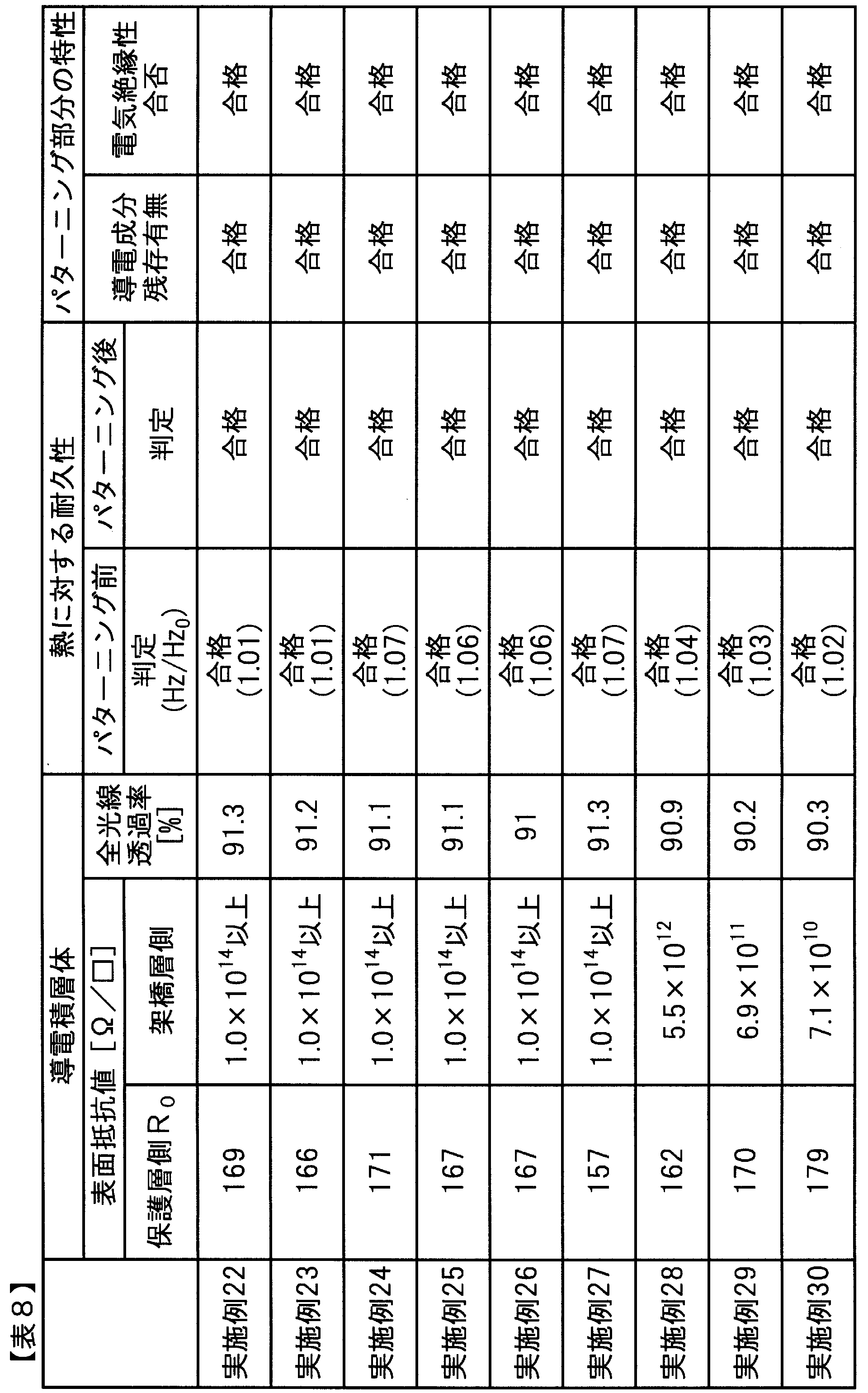


2:導電層
3:保護層
4:架橋層
5:積層面に垂直な方向より観察した導電面
6:単一の繊維状導電体(線上構造体の一例)
7:繊維状導電体の集合体(線上構造体の一例)
8:金属や金属酸化物のナノワイヤー(線上構造体の一例)
9:ウィスカーのような針状導電体(線上構造体の一例)
10:導電性薄膜
11:繊維状導電体の重なりよって形成した接点
12:金属や金属酸化物のナノワイヤーの重なりよって形成した接点
13:ウィスカーのような針状導電体の重なりよって形成した接点
14:導電層および保護層がパターン化された導電積層体
15:導電層および保護層がパターン化された導電積層体の基材
16:パターン化された導電層
17:パターン化された保護層
18:架橋層
19:接着剤や粘着剤等の接合層
20:タッチパネルの画面側の基材
21:タッチパネルの画面側の基材に積層したハードコート層
22:保護層表面
23:線状構造体が存在しない部分の保護層厚みt1
24:線状構造体の存在する部分の保護層厚みt2(単一の線状構造体の場合)
25:線状構造体の存在する部分の保護層厚みt2(線状構造体からなる集合体の場合)
26:集合体を形成する単一の線状構造体
27:線状構造体からなる集合体
28:基材
100:反応器
101:石英焼結板
102:密閉型触媒供給機
103:触媒投入ライン
104:原料ガス供給ライン
105:排ガスライン
106:加熱器
107:点検口
108:触媒
Claims (8)
- 基材の一方の面に架橋層を、基材のもう一方の面に導電層と、保護層とを積層した導電積層体であって、下記(i)~(iv)を満たす導電積層体;
(i)前記架橋層が、構造内に2個以上の重合反応に寄与する炭素-炭素二重結合基を有する化合物が重合反応した構造を含む架橋高分子からなり、かつ、前記架橋層の全質量に対する前記炭素-炭素二重結合基由来の構造の炭素-炭素二重結合基の単位構造部分の質量含有率が9~26質量%である;
(ii)前記架橋層の厚みが50nm~1μmである;
(iii)前記導電層が線状構造体からなるネットワーク構造を有する導電成分を含む;
(iv)前記保護層の平均厚みtが70nm~1μmである。 - 前記架橋層は、前記炭素-炭素二重結合基が重合反応した構造として、アクリロイル基が重合反応した構造を含む架橋高分子からなる請求項1に記載の導電積層体。
- 前記架橋層側と前記保護層側との間の、JIS C2151(2006)に基づいた静摩擦係数が0.75以下、かつ、JIS C2151(2006)に基づいた動摩擦係数が0.65以下である請求項1または2に記載の導電積層体。
- 前記架橋層面および前記保護層面のいずれかが、JIS L0849(2004)に基づいた方法にて試験用添付白布 綿(カナキン3号)によって50往復摩擦した際に、摩擦方向と平行方向に発生する傷の数が、2cm四方内に10個以下である請求項1~3のいずれかに記載の導電積層体。
- 前記架橋層側からC光源による光を入射したときのJIS Z8729(2004)に基づいたL*a*b*表示色系における透過光色調b*が1.5以下である請求項1~4のいずれかに記載の導電積層体。
- 前記架橋層側の表面抵抗値が1×10¹³Ω/□以下である請求項1~5のいずれかに記載の導電積層体。
- 前記基材の厚みが100μm以下である請求項1~6のいずれかに記載の導電積層体。
- 請求項1~7のいずれかに記載の導電積層体を用いた、タッチパネル。
Priority Applications (5)
| Application Number | Priority Date | Filing Date | Title |
|---|---|---|---|
| JP2012523537A JP5793142B2 (ja) | 2011-03-28 | 2012-03-27 | 導電積層体およびタッチパネル |
| EP12765039.8A EP2692525B1 (en) | 2011-03-28 | 2012-03-27 | Conductive laminated body and touch panel |
| KR1020137026546A KR20140009461A (ko) | 2011-03-28 | 2012-03-27 | 도전 적층체 및 터치 패널 |
| CN201280014292.3A CN103429427B (zh) | 2011-03-28 | 2012-03-27 | 导电层合体及触控面板 |
| US13/982,883 US20140008115A1 (en) | 2011-03-28 | 2012-03-27 | Conductive laminate and touch panel |
Applications Claiming Priority (2)
| Application Number | Priority Date | Filing Date | Title |
|---|---|---|---|
| JP2011069504 | 2011-03-28 | ||
| JP2011-069504 | 2011-03-28 |
Publications (1)
| Publication Number | Publication Date |
|---|---|
| WO2012133367A1 true WO2012133367A1 (ja) | 2012-10-04 |
Family
ID=46931084
Family Applications (1)
| Application Number | Title | Priority Date | Filing Date |
|---|---|---|---|
| PCT/JP2012/057860 Ceased WO2012133367A1 (ja) | 2011-03-28 | 2012-03-27 | 導電積層体およびタッチパネル |
Country Status (7)
| Country | Link |
|---|---|
| US (1) | US20140008115A1 (ja) |
| EP (1) | EP2692525B1 (ja) |
| JP (1) | JP5793142B2 (ja) |
| KR (1) | KR20140009461A (ja) |
| CN (1) | CN103429427B (ja) |
| TW (1) | TWI552871B (ja) |
| WO (1) | WO2012133367A1 (ja) |
Cited By (10)
| Publication number | Priority date | Publication date | Assignee | Title |
|---|---|---|---|---|
| JP5303069B2 (ja) * | 2011-08-03 | 2013-10-02 | 東レ株式会社 | 導電積層体、パターン化導電積層体およびそれを用いてなるタッチパネル |
| US20150111048A1 (en) * | 2013-10-17 | 2015-04-23 | Samsung Sdi Co., Ltd. | Transparent conductor and optical display including the same |
| JP2015165401A (ja) * | 2014-02-28 | 2015-09-17 | ティーピーケイ タッチ ソリューションズ(シアメン)インコーポレーテッド | 複合基板構造、及び、それを備えるタッチパネル |
| WO2015137278A1 (ja) * | 2014-03-14 | 2015-09-17 | 日立化成株式会社 | 感光性導電フィルム |
| JP2018086789A (ja) * | 2016-11-29 | 2018-06-07 | 凸版印刷株式会社 | 銀ナノ粒子積層体及び銀ナノ粒子積層体の製造方法 |
| JP2020132135A (ja) * | 2019-02-25 | 2020-08-31 | 現代自動車株式会社Hyundai Motor Company | 車両用タッチ式ボタン |
| US10795469B2 (en) * | 2013-10-16 | 2020-10-06 | Hitachi Chemical Company, Ltd. | Laminate containing conductive fiber, photosensitive conductive film, method for producing conductive pattern, conductive pattern substrate, and touch panel |
| US20200316916A1 (en) * | 2014-06-12 | 2020-10-08 | Toyo Ink Sc Holdings Co., Ltd. | Resin composition, laminate and laminate production method |
| WO2020203447A1 (ja) * | 2019-04-02 | 2020-10-08 | 東レ株式会社 | 導電層付き基材およびタッチパネル |
| JP2022143835A (ja) * | 2021-03-18 | 2022-10-03 | 日東電工株式会社 | 透明導電性フィルム |
Families Citing this family (35)
| Publication number | Priority date | Publication date | Assignee | Title |
|---|---|---|---|---|
| IN2014DN03390A (ja) | 2011-10-03 | 2015-06-05 | Hitachi Chemical Co Ltd | |
| WO2013084283A1 (ja) * | 2011-12-05 | 2013-06-13 | 日立化成株式会社 | タッチパネル用電極の保護膜の形成方法、感光性樹脂組成物及び感光性エレメント |
| WO2013084282A1 (ja) | 2011-12-05 | 2013-06-13 | 日立化成株式会社 | 樹脂硬化膜パターンの形成方法、感光性樹脂組成物及び感光性エレメント |
| KR102148154B1 (ko) * | 2013-01-22 | 2020-08-26 | 주식회사 동진쎄미켐 | 투명 전도성 막 코팅 조성물, 투명 전도성 막 및 투명 전도성 막의 제조 방법 |
| FR3010074B1 (fr) * | 2013-09-05 | 2019-08-02 | Saint-Gobain Glass France | Procede de fabrication d'un materiau comprenant un substrat muni d'une couche fonctionnelle a base d'oxyde d'etain et d'indium |
| KR102275893B1 (ko) * | 2014-03-07 | 2021-07-12 | 엘지이노텍 주식회사 | 터치 윈도우 |
| US9354659B2 (en) * | 2014-03-07 | 2016-05-31 | Lg Innotek Co., Ltd. | Touch window |
| KR102187469B1 (ko) * | 2014-03-07 | 2020-12-08 | 엘지이노텍 주식회사 | 터치 윈도우 |
| JP6526714B2 (ja) * | 2014-04-22 | 2019-06-05 | サビック グローバル テクノロジーズ ベスローテン フェンノートシャップ | ナノメートルサイズの金属粒子をポリマー表面に塗布するための紫外線硬化性転写コーティング |
| TWI486969B (zh) * | 2014-06-11 | 2015-06-01 | Nat Univ Tsing Hua | 複合導電材料的製作方法及其導電薄膜 |
| CN106661255A (zh) | 2014-08-07 | 2017-05-10 | 沙特基础工业全球技术有限公司 | 用于热成型应用的导电多层片材 |
| JP6301483B2 (ja) * | 2014-08-27 | 2018-03-28 | 富士フイルム株式会社 | 断熱フィルム、断熱フィルムの製造方法、断熱ガラスおよび窓 |
| CN105489313B (zh) * | 2014-09-17 | 2017-09-01 | 谢建德 | 高导电性基板及其制作方法 |
| CN104754263A (zh) * | 2014-11-26 | 2015-07-01 | 李正浩 | 新型智能数码屏幕 |
| KR20160087047A (ko) * | 2015-01-12 | 2016-07-21 | 삼성디스플레이 주식회사 | 표시 장치 |
| CN107205677B (zh) * | 2015-01-14 | 2020-12-25 | 东洋纺株式会社 | 伸缩性电极片、生物体信息计测用接触面 |
| TWI567757B (zh) * | 2015-06-03 | 2017-01-21 | 財團法人紡織產業綜合研究所 | 導電組成物 |
| WO2017046705A1 (en) * | 2015-09-14 | 2017-03-23 | Sabic Global Technologies B.V. | Conductive multilayer sheet for thermal forming and injection molding applications |
| KR102395991B1 (ko) * | 2015-10-29 | 2022-05-10 | 삼성전자주식회사 | 터치-지문 복합 센서를 포함하는 전자 기기 |
| ES2772256T3 (es) * | 2015-11-06 | 2020-07-07 | Meyer Burger Switzerland Ag | Láminas conductoras de polímero, celdas solares y métodos para producirlos |
| EP3427941B1 (en) * | 2016-03-11 | 2021-01-27 | Toray Industries, Inc. | Light-transmitting conductive laminate and light-transmitting conductive molded body using same |
| EP3541762B1 (en) | 2016-11-17 | 2022-03-02 | Cardinal CG Company | Static-dissipative coating technology |
| KR101801688B1 (ko) * | 2017-01-18 | 2017-11-27 | (주)이녹스첨단소재 | Oled 패널 하부 보호필름 및 이를 포함하는 oled 패널 |
| CN110325292A (zh) * | 2017-02-13 | 2019-10-11 | 泰克图斯科技公司 | 用于形成浇铸弹性体的方法 |
| FR3065652B1 (fr) * | 2017-04-27 | 2021-07-23 | Biomerieux Sa | Plaque d'analyse maldi-tof a support papier et son utilisation |
| CN109243677B (zh) * | 2018-07-27 | 2021-04-23 | 深圳市华科创智技术有限公司 | 一种透明导电膜 |
| CN109603206B (zh) * | 2018-12-09 | 2021-07-30 | 英鸿纳米科技股份有限公司 | 一种纳米纤维吸油材料 |
| JP7316071B2 (ja) * | 2019-03-18 | 2023-07-27 | 太陽ホールディングス株式会社 | 硬化性樹脂組成物、ドライフィルム、硬化物および電子部品 |
| KR102274135B1 (ko) * | 2019-04-29 | 2021-07-08 | 주식회사 아모그린텍 | 터치 스크린 패널 및 이의 제조방법 |
| CN110080857B (zh) * | 2019-05-22 | 2021-03-30 | 南通炜途汽车技术有限公司 | 一种汽车尾气除尘装置 |
| TWI759815B (zh) * | 2019-08-15 | 2022-04-01 | 國立清華大學 | 彈性導電柱體、製造方法及使用其的探針卡 |
| TW202116548A (zh) | 2019-10-28 | 2021-05-01 | 南亞塑膠工業股份有限公司 | 電子裝置外殼及其裝飾膜 |
| JP6773202B1 (ja) * | 2019-12-12 | 2020-10-21 | 東洋インキScホールディングス株式会社 | 透明導電性フィルム、光学部材、および電子機器 |
| EP4316815A4 (en) * | 2021-04-01 | 2025-04-02 | Toray Industries, Inc. | Laminate and manufacturing method of semiconductor device |
| US20260003447A1 (en) * | 2022-09-09 | 2026-01-01 | Contour Design Nordic A/S | Pointing device with flexible sleeve |
Citations (21)
| Publication number | Priority date | Publication date | Assignee | Title |
|---|---|---|---|---|
| JPH11198275A (ja) | 1998-01-16 | 1999-07-27 | Fuji Photo Film Co Ltd | 防曇用シート |
| JP2001243841A (ja) | 2000-02-29 | 2001-09-07 | Fuji Photo Film Co Ltd | 低反射透明導電性積層フイルム |
| JP2003115221A (ja) | 2001-10-05 | 2003-04-18 | Bridgestone Corp | 透明導電性フィルムとタッチパネル |
| JP3442082B2 (ja) | 1996-06-11 | 2003-09-02 | 住友大阪セメント株式会社 | 透明導電膜、低反射透明導電膜および表示装置 |
| JP3665969B2 (ja) | 2001-03-26 | 2005-06-29 | エイコス・インコーポレーテッド | カーボンナノチューブ含有フィルムの製造方法及びカーボンナノチューブ含有コーティング |
| JP2006328311A (ja) | 2005-05-30 | 2006-12-07 | Mitsubishi Rayon Co Ltd | 硬化性樹脂組成物、積層体、およびそれらの製造方法 |
| JP3879402B2 (ja) | 2000-12-28 | 2007-02-14 | ヤマハ株式会社 | 歌唱合成方法と装置及び記録媒体 |
| JP2007276322A (ja) | 2006-04-10 | 2007-10-25 | Toray Advanced Film Co Ltd | タッチパネル用透明導電性フィルム |
| JP2008222848A (ja) | 2007-03-13 | 2008-09-25 | Aica Kogyo Co Ltd | 紫外線硬化型ハードコート樹脂組成物および成形物 |
| JP2009505358A (ja) | 2005-08-12 | 2009-02-05 | カンブリオス テクノロジーズ コーポレイション | ナノワイヤに基づく透明導電体 |
| JP2009070660A (ja) | 2007-09-12 | 2009-04-02 | Kuraray Co Ltd | 透明導電膜およびその製造方法 |
| WO2009054464A1 (ja) * | 2007-10-26 | 2009-04-30 | Teijin Limited | 透明導電性積層体及び透明タッチパネル |
| JP2009146747A (ja) | 2007-12-14 | 2009-07-02 | Konica Minolta Holdings Inc | 透明補助電極フィルム及び透明補助電極フィルムの製造方法と、透明導電性フィルム及び透明導電性フィルムの製造方法 |
| JP2009155374A (ja) | 2007-12-25 | 2009-07-16 | Mitsubishi Rayon Co Ltd | 硬化性組成物、複合体、転写シート及びそれらの製造方法 |
| JP4349793B2 (ja) | 2002-11-25 | 2009-10-21 | 三菱樹脂株式会社 | 導電性樹脂積層フィルム及びその製造方法 |
| JP2009283376A (ja) | 2008-05-24 | 2009-12-03 | Kuraray Co Ltd | 電極基材、及びタッチパネル |
| JP2010507199A (ja) * | 2006-10-12 | 2010-03-04 | カンブリオス テクノロジーズ コーポレイション | ナノワイヤベースの透明導電体およびその適用 |
| JP4440720B2 (ja) | 2003-07-11 | 2010-03-24 | 旭硝子株式会社 | 光学フィルム |
| JP2010103212A (ja) * | 2008-10-22 | 2010-05-06 | Toray Ind Inc | 導電性フィルム及びそれを用いたディスプレイ用フィルター |
| JP2010205532A (ja) * | 2009-03-03 | 2010-09-16 | Konica Minolta Holdings Inc | 透明電極の製造方法、透明電極および有機エレクトロルミネッセンス素子 |
| JP2011029099A (ja) * | 2009-07-28 | 2011-02-10 | Panasonic Electric Works Co Ltd | 透明導電膜付き基材 |
Family Cites Families (8)
| Publication number | Priority date | Publication date | Assignee | Title |
|---|---|---|---|---|
| JP2005089622A (ja) * | 2003-09-18 | 2005-04-07 | Teijin Dupont Films Japan Ltd | 光学用ポリエステルフィルム |
| JP2007328092A (ja) * | 2006-06-07 | 2007-12-20 | Bridgestone Corp | 光学フィルタ、これを備えたディスプレイ及びプラズマディスプレイパネル |
| JP2007327065A (ja) * | 2007-07-31 | 2007-12-20 | Mitsubishi Polyester Film Copp | 積層ポリエステルフィルム |
| TW200923971A (en) * | 2007-09-12 | 2009-06-01 | Kuraray Co | Conductive films, conductive parts and manufacturing methods thereof |
| US7960027B2 (en) * | 2008-01-28 | 2011-06-14 | Honeywell International Inc. | Transparent conductors and methods for fabricating transparent conductors |
| JP2009252014A (ja) * | 2008-04-08 | 2009-10-29 | Kuraray Co Ltd | タッチパネル |
| JP5609008B2 (ja) * | 2009-05-12 | 2014-10-22 | コニカミノルタ株式会社 | 透明導電フィルム、透明導電フィルムの製造方法及び電子デバイス用透明電極 |
| CN101920955B (zh) * | 2009-06-09 | 2012-09-19 | 清华大学 | 碳纳米管膜保护结构及其制备方法 |
-
2012
- 2012-03-27 WO PCT/JP2012/057860 patent/WO2012133367A1/ja not_active Ceased
- 2012-03-27 US US13/982,883 patent/US20140008115A1/en not_active Abandoned
- 2012-03-27 CN CN201280014292.3A patent/CN103429427B/zh active Active
- 2012-03-27 EP EP12765039.8A patent/EP2692525B1/en not_active Not-in-force
- 2012-03-27 KR KR1020137026546A patent/KR20140009461A/ko not_active Ceased
- 2012-03-27 JP JP2012523537A patent/JP5793142B2/ja not_active Expired - Fee Related
- 2012-03-28 TW TW101110763A patent/TWI552871B/zh not_active IP Right Cessation
Patent Citations (21)
| Publication number | Priority date | Publication date | Assignee | Title |
|---|---|---|---|---|
| JP3442082B2 (ja) | 1996-06-11 | 2003-09-02 | 住友大阪セメント株式会社 | 透明導電膜、低反射透明導電膜および表示装置 |
| JPH11198275A (ja) | 1998-01-16 | 1999-07-27 | Fuji Photo Film Co Ltd | 防曇用シート |
| JP2001243841A (ja) | 2000-02-29 | 2001-09-07 | Fuji Photo Film Co Ltd | 低反射透明導電性積層フイルム |
| JP3879402B2 (ja) | 2000-12-28 | 2007-02-14 | ヤマハ株式会社 | 歌唱合成方法と装置及び記録媒体 |
| JP3665969B2 (ja) | 2001-03-26 | 2005-06-29 | エイコス・インコーポレーテッド | カーボンナノチューブ含有フィルムの製造方法及びカーボンナノチューブ含有コーティング |
| JP2003115221A (ja) | 2001-10-05 | 2003-04-18 | Bridgestone Corp | 透明導電性フィルムとタッチパネル |
| JP4349793B2 (ja) | 2002-11-25 | 2009-10-21 | 三菱樹脂株式会社 | 導電性樹脂積層フィルム及びその製造方法 |
| JP4440720B2 (ja) | 2003-07-11 | 2010-03-24 | 旭硝子株式会社 | 光学フィルム |
| JP2006328311A (ja) | 2005-05-30 | 2006-12-07 | Mitsubishi Rayon Co Ltd | 硬化性樹脂組成物、積層体、およびそれらの製造方法 |
| JP2009505358A (ja) | 2005-08-12 | 2009-02-05 | カンブリオス テクノロジーズ コーポレイション | ナノワイヤに基づく透明導電体 |
| JP2007276322A (ja) | 2006-04-10 | 2007-10-25 | Toray Advanced Film Co Ltd | タッチパネル用透明導電性フィルム |
| JP2010507199A (ja) * | 2006-10-12 | 2010-03-04 | カンブリオス テクノロジーズ コーポレイション | ナノワイヤベースの透明導電体およびその適用 |
| JP2008222848A (ja) | 2007-03-13 | 2008-09-25 | Aica Kogyo Co Ltd | 紫外線硬化型ハードコート樹脂組成物および成形物 |
| JP2009070660A (ja) | 2007-09-12 | 2009-04-02 | Kuraray Co Ltd | 透明導電膜およびその製造方法 |
| WO2009054464A1 (ja) * | 2007-10-26 | 2009-04-30 | Teijin Limited | 透明導電性積層体及び透明タッチパネル |
| JP2009146747A (ja) | 2007-12-14 | 2009-07-02 | Konica Minolta Holdings Inc | 透明補助電極フィルム及び透明補助電極フィルムの製造方法と、透明導電性フィルム及び透明導電性フィルムの製造方法 |
| JP2009155374A (ja) | 2007-12-25 | 2009-07-16 | Mitsubishi Rayon Co Ltd | 硬化性組成物、複合体、転写シート及びそれらの製造方法 |
| JP2009283376A (ja) | 2008-05-24 | 2009-12-03 | Kuraray Co Ltd | 電極基材、及びタッチパネル |
| JP2010103212A (ja) * | 2008-10-22 | 2010-05-06 | Toray Ind Inc | 導電性フィルム及びそれを用いたディスプレイ用フィルター |
| JP2010205532A (ja) * | 2009-03-03 | 2010-09-16 | Konica Minolta Holdings Inc | 透明電極の製造方法、透明電極および有機エレクトロルミネッセンス素子 |
| JP2011029099A (ja) * | 2009-07-28 | 2011-02-10 | Panasonic Electric Works Co Ltd | 透明導電膜付き基材 |
Non-Patent Citations (1)
| Title |
|---|
| See also references of EP2692525A4 |
Cited By (20)
| Publication number | Priority date | Publication date | Assignee | Title |
|---|---|---|---|---|
| JP5303069B2 (ja) * | 2011-08-03 | 2013-10-02 | 東レ株式会社 | 導電積層体、パターン化導電積層体およびそれを用いてなるタッチパネル |
| US10795469B2 (en) * | 2013-10-16 | 2020-10-06 | Hitachi Chemical Company, Ltd. | Laminate containing conductive fiber, photosensitive conductive film, method for producing conductive pattern, conductive pattern substrate, and touch panel |
| US20150111048A1 (en) * | 2013-10-17 | 2015-04-23 | Samsung Sdi Co., Ltd. | Transparent conductor and optical display including the same |
| US10115495B2 (en) * | 2013-10-17 | 2018-10-30 | Samsung Sdi Co., Ltd. | Transparent conductor and optical display including the same |
| US9760193B2 (en) | 2014-02-28 | 2017-09-12 | Tpk Touch Solutions (Xiamen) Inc. | Composite substrate structure and touch panel having the same |
| JP2015165401A (ja) * | 2014-02-28 | 2015-09-17 | ティーピーケイ タッチ ソリューションズ(シアメン)インコーポレーテッド | 複合基板構造、及び、それを備えるタッチパネル |
| US9709887B2 (en) | 2014-03-14 | 2017-07-18 | Hitachi Chemical Company, Ltd. | Photosensitive conductive film |
| JPWO2015137278A1 (ja) * | 2014-03-14 | 2017-04-06 | 日立化成株式会社 | 感光性導電フィルム |
| WO2015137278A1 (ja) * | 2014-03-14 | 2015-09-17 | 日立化成株式会社 | 感光性導電フィルム |
| US20200316916A1 (en) * | 2014-06-12 | 2020-10-08 | Toyo Ink Sc Holdings Co., Ltd. | Resin composition, laminate and laminate production method |
| JP2018086789A (ja) * | 2016-11-29 | 2018-06-07 | 凸版印刷株式会社 | 銀ナノ粒子積層体及び銀ナノ粒子積層体の製造方法 |
| JP2020132135A (ja) * | 2019-02-25 | 2020-08-31 | 現代自動車株式会社Hyundai Motor Company | 車両用タッチ式ボタン |
| JP7452987B2 (ja) | 2019-02-25 | 2024-03-19 | 現代自動車株式会社 | 車両用タッチ式ボタン |
| JP6773258B1 (ja) * | 2019-04-02 | 2020-10-21 | 東レ株式会社 | 導電層付き基材およびタッチパネル |
| TWI797437B (zh) * | 2019-04-02 | 2023-04-01 | 日商東麗股份有限公司 | 附有導電層之基材及觸控面板 |
| WO2020203447A1 (ja) * | 2019-04-02 | 2020-10-08 | 東レ株式会社 | 導電層付き基材およびタッチパネル |
| JP2022143835A (ja) * | 2021-03-18 | 2022-10-03 | 日東電工株式会社 | 透明導電性フィルム |
| KR20230142601A (ko) * | 2021-03-18 | 2023-10-11 | 닛토덴코 가부시키가이샤 | 투명 도전성 필름 |
| JP7485629B2 (ja) | 2021-03-18 | 2024-05-16 | 日東電工株式会社 | 透明導電性フィルム |
| KR102843527B1 (ko) * | 2021-03-18 | 2025-08-07 | 닛토덴코 가부시키가이샤 | 투명 도전성 필름 |
Also Published As
| Publication number | Publication date |
|---|---|
| TW201244933A (en) | 2012-11-16 |
| US20140008115A1 (en) | 2014-01-09 |
| TWI552871B (zh) | 2016-10-11 |
| JP5793142B2 (ja) | 2015-10-14 |
| EP2692525B1 (en) | 2015-10-28 |
| CN103429427A (zh) | 2013-12-04 |
| EP2692525A4 (en) | 2014-10-01 |
| CN103429427B (zh) | 2015-03-18 |
| EP2692525A1 (en) | 2014-02-05 |
| KR20140009461A (ko) | 2014-01-22 |
| JPWO2012133367A1 (ja) | 2014-07-28 |
Similar Documents
| Publication | Publication Date | Title |
|---|---|---|
| JP5793142B2 (ja) | 導電積層体およびタッチパネル | |
| JP5729298B2 (ja) | 導電積層体およびそれを用いてなるタッチパネル | |
| JP5428924B2 (ja) | 導電積層体およびそれを用いてなるタッチパネル | |
| JP5303069B2 (ja) | 導電積層体、パターン化導電積層体およびそれを用いてなるタッチパネル | |
| JP5423784B2 (ja) | 導電積層体およびその製造方法 | |
| CN103959397B (zh) | 导电层合体及使用该导电层合体而成的显示体 | |
| WO2014010270A1 (ja) | 導電積層体、パターン化導電積層体、その製造方法、および、それらを用いてなるタッチパネル | |
| JP2012183737A (ja) | 導電積層体およびそれを用いてなるタッチパネル | |
| JP2014102962A (ja) | 導電積層体、パターン化導電積層体、その製造方法、および、それらを用いてなるタッチパネル | |
| JP2013098066A (ja) | 導電積層体およびそれを用いてなるタッチパネル | |
| JP2012156094A (ja) | 導電積層体およびそれを用いてなるタッチパネル | |
| JP2013230564A (ja) | 透明導電積層体およびそれを用いてなる表示体 | |
| JP2014102963A (ja) | 導電積層体、パターン化導電積層体、その製造方法、および、それらを用いてなるタッチパネル |
Legal Events
| Date | Code | Title | Description |
|---|---|---|---|
| ENP | Entry into the national phase |
Ref document number: 2012523537 Country of ref document: JP Kind code of ref document: A |
|
| 121 | Ep: the epo has been informed by wipo that ep was designated in this application |
Ref document number: 12765039 Country of ref document: EP Kind code of ref document: A1 |
|
| WWE | Wipo information: entry into national phase |
Ref document number: 13982883 Country of ref document: US |
|
| WWE | Wipo information: entry into national phase |
Ref document number: 2012765039 Country of ref document: EP |
|
| NENP | Non-entry into the national phase |
Ref country code: DE |
|
| ENP | Entry into the national phase |
Ref document number: 20137026546 Country of ref document: KR Kind code of ref document: A |