WO2012133778A1 - 金属系粒子集合体 - Google Patents
金属系粒子集合体 Download PDFInfo
- Publication number
- WO2012133778A1 WO2012133778A1 PCT/JP2012/058599 JP2012058599W WO2012133778A1 WO 2012133778 A1 WO2012133778 A1 WO 2012133778A1 JP 2012058599 W JP2012058599 W JP 2012058599W WO 2012133778 A1 WO2012133778 A1 WO 2012133778A1
- Authority
- WO
- WIPO (PCT)
- Prior art keywords
- metal
- particle assembly
- based particle
- particles
- average
- Prior art date
- Legal status (The legal status is an assumption and is not a legal conclusion. Google has not performed a legal analysis and makes no representation as to the accuracy of the status listed.)
- Ceased
Links
Images




Classifications
-
- G—PHYSICS
- G02—OPTICS
- G02B—OPTICAL ELEMENTS, SYSTEMS OR APPARATUS
- G02B5/00—Optical elements other than lenses
- G02B5/008—Surface plasmon devices
-
- B—PERFORMING OPERATIONS; TRANSPORTING
- B82—NANOTECHNOLOGY
- B82Y—SPECIFIC USES OR APPLICATIONS OF NANOSTRUCTURES; MEASUREMENT OR ANALYSIS OF NANOSTRUCTURES; MANUFACTURE OR TREATMENT OF NANOSTRUCTURES
- B82Y20/00—Nanooptics, e.g. quantum optics or photonic crystals
-
- H—ELECTRICITY
- H10—SEMICONDUCTOR DEVICES; ELECTRIC SOLID-STATE DEVICES NOT OTHERWISE PROVIDED FOR
- H10F—INORGANIC SEMICONDUCTOR DEVICES SENSITIVE TO INFRARED RADIATION, LIGHT, ELECTROMAGNETIC RADIATION OF SHORTER WAVELENGTH OR CORPUSCULAR RADIATION
- H10F77/00—Constructional details of devices covered by this subclass
- H10F77/30—Coatings
- H10F77/306—Coatings for devices having potential barriers
- H10F77/311—Coatings for devices having potential barriers for photovoltaic cells
- H10F77/315—Coatings for devices having potential barriers for photovoltaic cells the coatings being antireflective or having enhancing optical properties
-
- H—ELECTRICITY
- H10—SEMICONDUCTOR DEVICES; ELECTRIC SOLID-STATE DEVICES NOT OTHERWISE PROVIDED FOR
- H10F—INORGANIC SEMICONDUCTOR DEVICES SENSITIVE TO INFRARED RADIATION, LIGHT, ELECTROMAGNETIC RADIATION OF SHORTER WAVELENGTH OR CORPUSCULAR RADIATION
- H10F77/00—Constructional details of devices covered by this subclass
- H10F77/40—Optical elements or arrangements
- H10F77/42—Optical elements or arrangements directly associated or integrated with photovoltaic cells, e.g. light-reflecting means or light-concentrating means
- H10F77/48—Back surface reflectors [BSR]
-
- H—ELECTRICITY
- H10—SEMICONDUCTOR DEVICES; ELECTRIC SOLID-STATE DEVICES NOT OTHERWISE PROVIDED FOR
- H10K—ORGANIC ELECTRIC SOLID-STATE DEVICES
- H10K50/00—Organic light-emitting devices
- H10K50/80—Constructional details
- H10K50/805—Electrodes
-
- H—ELECTRICITY
- H10—SEMICONDUCTOR DEVICES; ELECTRIC SOLID-STATE DEVICES NOT OTHERWISE PROVIDED FOR
- H10K—ORGANIC ELECTRIC SOLID-STATE DEVICES
- H10K50/00—Organic light-emitting devices
- H10K50/80—Constructional details
- H10K50/85—Arrangements for extracting light from the devices
-
- C—CHEMISTRY; METALLURGY
- C08—ORGANIC MACROMOLECULAR COMPOUNDS; THEIR PREPARATION OR CHEMICAL WORKING-UP; COMPOSITIONS BASED THEREON
- C08G—MACROMOLECULAR COMPOUNDS OBTAINED OTHERWISE THAN BY REACTIONS ONLY INVOLVING UNSATURATED CARBON-TO-CARBON BONDS
- C08G2261/00—Macromolecular compounds obtained by reactions forming a carbon-to-carbon link in the main chain of the macromolecule
- C08G2261/30—Monomer units or repeat units incorporating structural elements in the main chain
- C08G2261/31—Monomer units or repeat units incorporating structural elements in the main chain incorporating aromatic structural elements in the main chain
- C08G2261/314—Condensed aromatic systems, e.g. perylene, anthracene or pyrene
- C08G2261/3142—Condensed aromatic systems, e.g. perylene, anthracene or pyrene fluorene-based, e.g. fluorene, indenofluorene, or spirobifluorene
-
- C—CHEMISTRY; METALLURGY
- C08—ORGANIC MACROMOLECULAR COMPOUNDS; THEIR PREPARATION OR CHEMICAL WORKING-UP; COMPOSITIONS BASED THEREON
- C08G—MACROMOLECULAR COMPOUNDS OBTAINED OTHERWISE THAN BY REACTIONS ONLY INVOLVING UNSATURATED CARBON-TO-CARBON BONDS
- C08G2261/00—Macromolecular compounds obtained by reactions forming a carbon-to-carbon link in the main chain of the macromolecule
- C08G2261/30—Monomer units or repeat units incorporating structural elements in the main chain
- C08G2261/32—Monomer units or repeat units incorporating structural elements in the main chain incorporating heteroaromatic structural elements in the main chain
- C08G2261/322—Monomer units or repeat units incorporating structural elements in the main chain incorporating heteroaromatic structural elements in the main chain non-condensed
- C08G2261/3223—Monomer units or repeat units incorporating structural elements in the main chain incorporating heteroaromatic structural elements in the main chain non-condensed containing one or more sulfur atoms as the only heteroatom, e.g. thiophene
-
- C—CHEMISTRY; METALLURGY
- C08—ORGANIC MACROMOLECULAR COMPOUNDS; THEIR PREPARATION OR CHEMICAL WORKING-UP; COMPOSITIONS BASED THEREON
- C08G—MACROMOLECULAR COMPOUNDS OBTAINED OTHERWISE THAN BY REACTIONS ONLY INVOLVING UNSATURATED CARBON-TO-CARBON BONDS
- C08G2261/00—Macromolecular compounds obtained by reactions forming a carbon-to-carbon link in the main chain of the macromolecule
- C08G2261/30—Monomer units or repeat units incorporating structural elements in the main chain
- C08G2261/32—Monomer units or repeat units incorporating structural elements in the main chain incorporating heteroaromatic structural elements in the main chain
- C08G2261/324—Monomer units or repeat units incorporating structural elements in the main chain incorporating heteroaromatic structural elements in the main chain condensed
- C08G2261/3246—Monomer units or repeat units incorporating structural elements in the main chain incorporating heteroaromatic structural elements in the main chain condensed containing nitrogen and sulfur as heteroatoms
-
- C—CHEMISTRY; METALLURGY
- C08—ORGANIC MACROMOLECULAR COMPOUNDS; THEIR PREPARATION OR CHEMICAL WORKING-UP; COMPOSITIONS BASED THEREON
- C08G—MACROMOLECULAR COMPOUNDS OBTAINED OTHERWISE THAN BY REACTIONS ONLY INVOLVING UNSATURATED CARBON-TO-CARBON BONDS
- C08G2261/00—Macromolecular compounds obtained by reactions forming a carbon-to-carbon link in the main chain of the macromolecule
- C08G2261/30—Monomer units or repeat units incorporating structural elements in the main chain
- C08G2261/34—Monomer units or repeat units incorporating structural elements in the main chain incorporating partially-aromatic structural elements in the main chain
- C08G2261/342—Monomer units or repeat units incorporating structural elements in the main chain incorporating partially-aromatic structural elements in the main chain containing only carbon atoms
- C08G2261/3422—Monomer units or repeat units incorporating structural elements in the main chain incorporating partially-aromatic structural elements in the main chain containing only carbon atoms conjugated, e.g. PPV-type
-
- C—CHEMISTRY; METALLURGY
- C08—ORGANIC MACROMOLECULAR COMPOUNDS; THEIR PREPARATION OR CHEMICAL WORKING-UP; COMPOSITIONS BASED THEREON
- C08G—MACROMOLECULAR COMPOUNDS OBTAINED OTHERWISE THAN BY REACTIONS ONLY INVOLVING UNSATURATED CARBON-TO-CARBON BONDS
- C08G2261/00—Macromolecular compounds obtained by reactions forming a carbon-to-carbon link in the main chain of the macromolecule
- C08G2261/90—Applications
- C08G2261/95—Use in organic luminescent diodes
-
- Y—GENERAL TAGGING OF NEW TECHNOLOGICAL DEVELOPMENTS; GENERAL TAGGING OF CROSS-SECTIONAL TECHNOLOGIES SPANNING OVER SEVERAL SECTIONS OF THE IPC; TECHNICAL SUBJECTS COVERED BY FORMER USPC CROSS-REFERENCE ART COLLECTIONS [XRACs] AND DIGESTS
- Y02—TECHNOLOGIES OR APPLICATIONS FOR MITIGATION OR ADAPTATION AGAINST CLIMATE CHANGE
- Y02E—REDUCTION OF GREENHOUSE GAS [GHG] EMISSIONS, RELATED TO ENERGY GENERATION, TRANSMISSION OR DISTRIBUTION
- Y02E10/00—Energy generation through renewable energy sources
- Y02E10/50—Photovoltaic [PV] energy
- Y02E10/52—PV systems with concentrators
-
- Y—GENERAL TAGGING OF NEW TECHNOLOGICAL DEVELOPMENTS; GENERAL TAGGING OF CROSS-SECTIONAL TECHNOLOGIES SPANNING OVER SEVERAL SECTIONS OF THE IPC; TECHNICAL SUBJECTS COVERED BY FORMER USPC CROSS-REFERENCE ART COLLECTIONS [XRACs] AND DIGESTS
- Y10—TECHNICAL SUBJECTS COVERED BY FORMER USPC
- Y10T—TECHNICAL SUBJECTS COVERED BY FORMER US CLASSIFICATION
- Y10T428/00—Stock material or miscellaneous articles
- Y10T428/12—All metal or with adjacent metals
- Y10T428/12014—All metal or with adjacent metals having metal particles
-
- Y—GENERAL TAGGING OF NEW TECHNOLOGICAL DEVELOPMENTS; GENERAL TAGGING OF CROSS-SECTIONAL TECHNOLOGIES SPANNING OVER SEVERAL SECTIONS OF THE IPC; TECHNICAL SUBJECTS COVERED BY FORMER USPC CROSS-REFERENCE ART COLLECTIONS [XRACs] AND DIGESTS
- Y10—TECHNICAL SUBJECTS COVERED BY FORMER USPC
- Y10T—TECHNICAL SUBJECTS COVERED BY FORMER US CLASSIFICATION
- Y10T428/00—Stock material or miscellaneous articles
- Y10T428/24—Structurally defined web or sheet [e.g., overall dimension, etc.]
- Y10T428/24355—Continuous and nonuniform or irregular surface on layer or component [e.g., roofing, etc.]
- Y10T428/24372—Particulate matter
- Y10T428/24413—Metal or metal compound
Definitions
- the present invention is useful for improving the light emission efficiency of light emitting elements (such as organic EL (electroluminescence) elements, inorganic EL elements, inorganic LED (light emitting diode) elements), and improving the conversion efficiency of photoelectric conversion elements (solar cell elements).
- light emitting elements such as organic EL (electroluminescence) elements, inorganic EL elements, inorganic LED (light emitting diode) elements
- photoelectric conversion elements solar cell elements.
- the present invention relates to a metal particle aggregate that is a plasmonic material.
- Plasmon is a free-electron rough wave generated by collective oscillation of free electrons in a metal nanostructure.
- plasmonics In recent years, the above-mentioned technical field dealing with plasmons is called “plasmonics” and has attracted a great deal of attention and has been actively researched. Such research has been conducted on light-emitting elements using localized plasmon resonance phenomenon of metal nanoparticles. Including those for the purpose of improving luminous efficiency and improving the conversion efficiency of photoelectric conversion elements (solar cell elements).
- Patent Document 1 Japanese Patent Application Laid-Open No. 2007-139540
- Patent Document 2 Japanese Patent Application Laid-Open No. 08-271431
- Patent Document 3 International Publication No. 2005/033335
- Patent Document 3 utilize the localized plasmon resonance phenomenon.
- a technique for enhancing fluorescence is disclosed.
- T. Fukuura and M. Kawasaki “Long Range Enhancement of Molecular Fluorescence by Closely Packed Submicro-scale Ag Islands”, e-Journal of Surface Science and Nanotechnology, 2009, 7, 653
- Non-Patent Document 1 Studies on localized plasmon resonance by silver nanoparticles are shown.
- JP 2007-139540 A Japanese Patent Application Laid-Open No. 08-271431 International Publication No. 2005/033335
- an object of the present invention is to provide a novel plasmon material (plasmonic material) exhibiting extremely strong plasmon resonance.
- Patent Document 1 paragraphs 0010 to 0011
- the particle size is about 500 nm.
- the luminous efficiency ⁇ is theoretically about 1
- such a silver particle does not exhibit a light emission enhancing action in practice.
- the reason why such large silver particles show almost no light emission enhancement is because the surface free electrons in the silver particles are so large that the bipolars seen in general nanoparticles (relatively small nanoparticles) This is presumably because child-type localized plasmons hardly occur.
- the enhancement effect by plasmons can be dramatically improved.
- the present invention includes the following.
- the metal-based particles have an average particle diameter in the range of 200 to 1600 nm, an average height in the range of 55 to 500 nm, and an aspect ratio defined by a ratio of the average particle diameter to the average height of 1 to 8 In the range of In the absorption spectrum in the visible light region, all of the metal particles made of the same particle size, the same height and the same material as the average particle diameter are within the range of 1 to 2 ⁇ m.
- a metal-based particle assembly film multilayer substrate comprising a substrate and a film made of the metal-based particle assembly according to any one of [1] to [4], which is stacked on the substrate.
- An optical element comprising a body film laminated substrate.
- An optical element comprising a film laminated substrate.
- the light absorption layer is a concept including, for example, a light absorption layer that is an active layer of a photoelectric conversion element (solar cell element) and a light emission layer that is an active layer of a light emitting element.
- the metal-based particle assembly and the metal-based particle assembly film-laminated substrate of the present invention exhibit extremely strong plasmon resonance as compared with conventional plasmon materials.
- Such metal-based particle assembly and metal-based particle assembly film laminated substrate of the present invention are extremely useful as an enhancement element for optical elements including light-emitting elements, photoelectric conversion elements (solar cell elements), and the like. Luminous efficiency and conversion efficiency can be significantly improved.
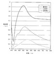
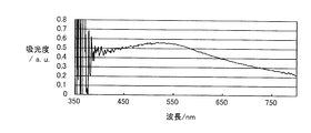
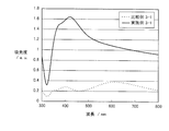
- FIG. 2 is an absorption spectrum of the metal-based particle assembly film laminated substrate obtained in Example 1 and Comparative Examples 1 and 2.
- FIG. 4 is an absorption spectrum of the metal-based particle assembly film laminated substrate obtained in Example 2. It is a schematic flowchart which shows the manufacturing method of a reference metal type particle aggregate. It is a SEM image (20000 times and 50000 times scale) when the reference metal type particle assembly film in a reference metal type particle assembly film lamination substrate is seen from right above. It is a figure explaining the absorption-spectrum measuring method using the objective lens (100 times) of a microscope. It is the absorption spectrum of the metal type particle assembly film
- FIG. 6 is an SEM image (10,000 times scale) when the metal-based particle assembly film in the metal-based particle assembly film laminated substrate obtained in Comparative Example 3-1 is viewed from directly above.
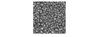
- 3 is an AFM image of a metal-based particle assembly film in a metal-based particle assembly film laminated substrate obtained in Comparative Example 3-1.
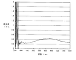
- FIG. 5 is an absorption spectrum of the metal-based particle assembly film laminated substrate obtained in Example 3-1 and Comparative Example 3-1 by a measuring method using an integrating sphere spectrophotometer.
- FIG. 6 is an absorption spectrum of the metal-based particle assembly film laminated substrate obtained in Comparative Example 3-1 by a measuring method using a microscope objective lens (100 times).
- FIG. 6 is an SEM image (10,000 times and 50000 times scale) when the metal-based particle assembly film in the metal-based particle assembly film laminated substrate obtained in Comparative Example 9-1 is viewed from directly above.
- 7 is an AFM image of a metal-based particle assembly film in a metal-based particle assembly film laminated substrate obtained in Comparative Example 9-1.
- FIG. 6 is an absorption spectrum of the metal-based particle assembly film laminated substrate obtained in Comparative Example 9-1.
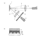
- FIG. 19A is a schematic diagram showing a measurement system of an emission spectrum of a photoexcited light emitting device
- FIG. 19B is a schematic cross-sectional view showing a photoexcited light emitting device having a metal-based particle assembly film and an insulating layer.
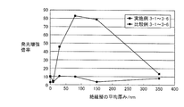
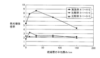
- FIG. 6 is a diagram comparing the light emission enhancing effect of the photoexcited light emitting devices of Examples 3-1 to 3-6 and the light emission enhancing effect of the photoexcited light emitting devices of Comparative Examples 3-1 to 3-6.
- the light emission enhancement effect in the light excitation light emitting devices of Examples 4-1 to 4-5 is compared with the light emission enhancement effect in the light excitation light emission devices of Comparative Examples 5-1 to 5-5 and Comparative Examples 9-1 to 9-5.
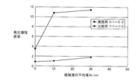
- FIG. FIG. 6 is a diagram comparing the light emission enhancing effect of the photoexcited light emitting devices of Examples 5-1 to 5-3 and the light emission enhancing effect of the photoexcited light emitting devices of Comparative Examples 7-1 to 7-3.
- the metal-based particle aggregate of the present invention is a particle aggregate in which 30 or more metal-based particles are two-dimensionally arranged apart from each other.
- the metal-based particles constituting the aggregate have an aspect ratio defined by the ratio of the average particle diameter to the average height within an average particle diameter of 200 to 1600 nm, an average height of 55 to 500 nm. It is in the range of 1-8.
- the metal-based particle assembly of the present invention comprises a metal-based particle composed of the same material as the average particle diameter, the same height as the average particle, and the same material in the absorption spectrum in the visible light region.
- the absorbance at the maximum wavelength of the peak on the longest wavelength side is larger than that of the reference metal particle aggregate arranged so that the distance between the particles is all within the range of 1 to 2 ⁇ m. high.
- the metal-based particle assembly film laminated substrate of the present invention is obtained by laminating (carrying) the metal-based particle assembly on a substrate.
- the average particle diameter and average height of the metal-based particle aggregate are “same” as that of the reference metal-based particle aggregate means that the difference in average particle diameter is within a range of ⁇ 5 nm, This means that the difference in thickness is within a range of ⁇ 10 nm.
- a plasmon resonance peak (hereinafter also referred to as a plasmon peak) is observed as a peak in the ultraviolet to visible region, and the absorbance value at the maximum wavelength of the plasmon peak is The strength of plasmon resonance of the plasmon material can be evaluated roughly.
- the plasmon material (metal-based particle assembly and metal-based particle assembly film laminated substrate) of the present invention has an absorbance at the maximum wavelength of the peak on the longest wavelength side in the visible light region which is such a plasmon peak.
- the size and shape of the metal particles constituting the metal particle aggregate and the average distance between the metal particles are important in the plasmon material of the present invention.
- the characteristics relating to the absorbance can be expressed by controlling the size and shape of the metal-based particles and / or the average distance between the metal-based particles.
- the absorption spectrum of the metal-based particle aggregate is measured in a state of being laminated on a glass substrate (that is, as a metal-based particle aggregate film-laminated glass substrate) by an absorptiometry.
- the absorption spectrum is on the back side of the metal-based particle assembly film laminated glass substrate (on the side opposite to the metal-based particle assembly film), and is in the ultraviolet to visible light region from the direction perpendicular to the substrate surface.
- the reference metal-based particle aggregate is an average particle diameter of the metal-based particle aggregate that is an object of absorption spectrum measurement, a metal particle A having the same particle size, height, and the same material as the average height. Is a metal-based particle aggregate arranged so that all the distances are within the range of 1 to 2 ⁇ m, and is large enough to measure the absorption spectrum using the above-mentioned microscope in the state of being laminated on the glass substrate. It is what you have.
- the absorbance at the maximum wavelength of the peak on the longest wavelength side between the metal particle aggregate to be measured for absorption spectrum and the reference metal particle aggregate is used as a comparison target.
- the absorption spectrum of each of the metal-based particle assembly and the reference metal-based particle assembly is obtained, and the absorbance at the maximum wavelength of the peak on the longest wavelength side in each absorption spectrum is expressed as the respective coverage (metal-based). The value divided by the coverage of the substrate surface by the particles is calculated and compared.
- the absorption spectrum of the metal-based particle aggregate of the present invention is measured by an absorptiometry in a state where it is stacked on a substrate (glass substrate) (that is, as a metal-based particle assembly film laminated glass substrate), visible light is obtained.
- the absorbance at the maximum wavelength of the plasmon peak on the longest wavelength side in the region can be 1 or more, further 1.5 or more, and even more preferably about 2.
- the plasmon material (metal particle aggregate and metal particle aggregate film laminated substrate) of the present invention is capable of two-dimensionally transferring a specific number or more of relatively large metal particles in which the metal particle aggregate has a specific shape.
- the plasmon resonance may have the following special features due to having a structure spaced apart from each other.
- the action range of plasmon resonance (the range in which the plasmon enhances) can be significantly extended. That is, in the plasmon material of the present invention in which 30 or more metal particles having a predetermined shape are two-dimensionally arranged, the range of plasmon resonance can be significantly extended by the interaction of the individual metal particles. Such an elongation effect is also considered to be expressed by the interaction between the localized plasmons of the metal-based particles.
- the factors of the light emission enhancing action are as follows: 1) The electric field in the vicinity of the particles is enhanced by the occurrence of localized plasmons in the metal nanoparticles (first). Induction of greater luminescence than the luminescent dipole of the excited molecule by exciting the vibrational mode of free electrons in the metal nanoparticle by energy transfer from the excited molecule. There are two factors: a dipole occurs in the metal nanoparticle, which increases the emission quantum efficiency itself (second factor).
- the distance between the metal nanoparticles and the excited molecule is It is necessary that the energy transfer by the Dexter mechanism, which is direct movement, does not occur, and is within the range in which the energy transfer of the Förster mechanism appears, which is approximately 1 nm to 10 nm. This is because the occurrence of the luminescence-induced dipole is based on Förster energy transfer theory (see Non-Patent Document 1 above).
- the distance between the metal nanoparticle and the molecule to be excited is closer within the range of 1 nm to 10 nm, the luminescence-induced dipole is more likely to occur and the emission enhancement effect is enhanced.
- the luminescence enhancement effect gradually weakens due to the fact that the localized plasmon resonance does not effectively affect, and when the energy transfer of the Förster mechanism is exceeded (generally, at a distance of about 10 nm or more).
- the distance between the metal nanoparticles effective for obtaining an effective light emission enhancement effect and the excited molecule is set to 10 nm or less.
- a light-emitting element or a photoelectric conversion element usually has an active layer (for example, a light-emitting layer of a light-emitting element or a light absorption layer of a photoelectric conversion element) having a thickness of several tens of nm or more. Even if it can be arranged close to or in the active layer, the direct enhancement effect by localized plasmon resonance can be obtained only in a small part of the active layer.
- the range of plasmon resonance which was conventionally limited to the range of about the Forster distance (about 10 nm or less), to about several hundred nm, for example.
- the extension of the plasmon resonance operating range as described above is extremely advantageous for enhancing optical elements such as light emitting elements and photoelectric conversion elements (solar electronic elements). That is, it is possible to reinforce the entire active layer (such as a light emitting layer in a light emitting element or a light absorbing layer in a photoelectric conversion element) having a thickness of usually several tens of nanometers or more by greatly extending the working range. Thereby, the enhancement effect (emission efficiency, conversion efficiency, etc.) of the optical element can be remarkably improved.
- the plasmon material has to be arranged so that the distance from the active layer is within the range of the Förster distance.
- the distance from the active layer is within the range of the Förster distance.
- 10 nm Can be enhanced by plasmon resonance even if they are arranged at a position several tens of nm (for example, 20 nm) or even several hundred nm apart.
- a plasmon material metal particle aggregate
- the plasmon material In a conventional light emitting device using a plasmon material, the plasmon material has to be disposed very close to the light emitting layer, and the distance between the plasmon material and the light extraction surface is greatly separated, so that the generated light is incident on the light extraction surface. In the meantime, most of the light is totally reflected at the interfaces of the various light-emitting element constituent layers that pass therethrough, and the light extraction efficiency may become extremely small.
- the maximum wavelength of the plasmon peak shows a unique shift depending on the average particle diameter of the metal-based particles and the average distance between the particles. Specifically, the maximum wavelength of the plasmon peak on the longest wavelength side in the visible light region shifts to the short wavelength side (blue shift) as the average particle size of the metal-based particles is increased with a constant average distance between the particles. ) Similarly, as the average particle size of the large metal particles is kept constant and the average distance between the particles is reduced (when the metal particles are arranged more densely), the plasmon peak on the longest wavelength side in the visible light region is reduced. The maximum wavelength shifts to the short wavelength side. This unique phenomenon is due to the Mie scattering theory generally accepted for plasmon materials (according to this theory, the maximum wavelength of the plasmon peak shifts to the longer wavelength side (red shift) as the particle size increases). It is contrary.
- the unique blue shift as described above also has a structure in which a specific number or more of relatively large metal particles having a specific shape are arranged two-dimensionally apart from each other in the metal particle aggregate of the present invention. This is considered to be due to the interaction between the local plasmons of the metal-based particles.
- the metal-based particle aggregate of the present invention (stacked on a glass substrate) has the longest absorption spectrum in the visible light region measured by absorptiometry depending on the shape of the metal-based particles and the distance between the particles.
- the plasmon peak on the wavelength side can exhibit a maximum wavelength in a wavelength region of 350 to 550 nm, for example.
- the metal-based particle assembly of the present invention typically has a size of about 30 to 500 nm (for example 30 to 30 nm) as compared with the case where the metal-based particles are arranged with a sufficiently long inter-particle distance (for example 1 ⁇ m). 250 nm).
- the plasmon material of the present invention in which the maximum wavelength of the plasmon peak is blue-shifted compared with the conventional one is extremely advantageous in the following points. That is, while there is a strong demand for a blue (or near-wavelength region, hereinafter the same) luminescent material (especially a blue phosphorescent material) that exhibits high luminous efficiency, development of such a material that can withstand practical use is currently underway. Even when using a blue light emitting material having a relatively low luminous efficiency by applying the plasmon material of the present invention having a plasmon peak in a blue wavelength region as an enhancement element to a light emitting element, for example, The luminous efficiency can be increased to a sufficient level. Further, when applied to a photoelectric conversion element (solar cell element), for example, by blue shifting the resonance wavelength, a wavelength region that could not be used in the active layer itself can be used effectively, and conversion efficiency can be improved. .
- a photoelectric conversion element solar cell element
- the metal-based particles constituting the metal-based particle assembly and the metal-based particle assembly film laminated substrate are nanoparticles or aggregates thereof, a plasmon peak is observed in the ultraviolet to visible region in the absorption spectrum measurement by absorptiometry.
- a plasmon peak is observed in the ultraviolet to visible region in the absorption spectrum measurement by absorptiometry.
- noble metals such as gold, silver, copper, platinum, and palladium are preferable, and silver is more preferable because it is inexpensive and has low absorption (small imaginary part of dielectric function at visible light wavelength).
- the average particle diameter of the metal-based particles is in the range of 200 to 1600 nm, and the above-mentioned characteristics related to absorbance (characteristic that the absorbance at the maximum wavelength of the plasmon peak on the longest wavelength side is larger than that of the reference metal-based particle aggregate
- it is preferably in the range of 200 to 1200 nm, more preferably 250 to 500 nm, and still more preferably 300 to 500 nm.
- it is extremely important in the present invention to use relatively large metal-based particles, and by forming an aggregate in which a predetermined number (30) or more of large metal particles are two-dimensionally arranged. Therefore, it is possible to realize extremely strong plasmon resonance, further significantly extending the range of action of plasmon resonance, and shifting the plasmon peak to the short wavelength side.
- the average particle size of the metal-based particles referred to here is a random selection of 10 particles in the SEM observation image directly above the metal-based particle aggregate (film) in which the metal-based particles are two-dimensionally arranged.
- Randomly draw 5 tangent diameters in each particle image (however, any straight line with a tangent diameter can only pass through the inside of the particle image, one of which goes only inside the particle and is the longest drawn straight line)
- the average value of the 10 selected particle sizes when the average value is the particle size of each particle.
- the tangent diameter is defined as a perpendicular line connecting the interval (projection image) of a particle between two parallel lines in contact with it (Nikkan Kogyo Shimbun, “Particle Measurement Technology”, 1994, page 5). .
- the average height of the metal-based particles is in the range of 55 to 500 nm, and in order to effectively obtain the above characteristics relating to absorbance, and further the above characteristics (1) to (2), preferably 55 to 300 nm. Preferably, it is in the range of 70 to 150 nm.
- the average height of the metal-based particles is 10 particles when 10 particles are randomly selected in the AFM observation image of the metal-based particle aggregate (film) and the heights of these 10 particles are measured. It is an average value of measured values.
- the aspect ratio of the metal-based particles is in the range of 1 to 8, and preferably 2 to 8, more preferably, in order to effectively obtain the above-mentioned characteristics relating to absorbance, and further the above-mentioned characteristics (1) to (2). Is in the range of 2.5-8.
- the aspect ratio of the metal-based particles is defined by the ratio of the average particle diameter to the average height (average particle diameter / average height).
- the metallic particles may be spherical, but preferably have a flat shape with an aspect ratio exceeding 1.
- the metal particles preferably have a smooth curved surface, and more preferably have a flat shape with a smooth curved surface. Some minute irregularities (roughness) may be included, and in this sense, the metal-based particles may be indefinite.
- the size and shape (average particle diameter, average height, aspect ratio) of the metal particles constituting the metal particle aggregate should be as uniform as possible. Is preferred. That is, by making the size and shape of the metal-based particles uniform, the plasmon peak is sharpened, and accordingly, the absorbance of the plasmon peak on the longest wavelength side tends to be larger than that of the reference metal-based particle aggregate. Become.
- the reduction in the variation in size and shape between the metal-based particles is also advantageous from the viewpoint of the uniformity of the intensity of plasmon resonance in the plane of the metal-based particle aggregate (film). However, even if there is some variation in the particle size, it is not preferable that the distance between the large particles is increased, and it is preferable that the interaction between the large particles is facilitated by filling the space between the small particles.
- the metal-based particles have an average distance (hereinafter also referred to as an average inter-particle distance) of 1 to 150 nm with the adjacent metal-based particles. It is preferable that they are arranged so as to be inside. More preferably, it is in the range of 1 to 100 nm, still more preferably 1 to 50 nm, and particularly preferably 1 to 20 nm.
- the metal-based particles densely as described above, the interaction between the localized plasmons of the metal-based particles is effectively generated, and the above-mentioned characteristics relating to the absorbance, and further the characteristics (1) to (2) described above are achieved. It can be expressed effectively.
- the average interparticle distance is less than 1 nm, electron transfer based on the Dexter mechanism occurs between particles, which is disadvantageous in terms of deactivation of localized plasmons.
- the average inter-particle distance here is selected by selecting 30 particles at random in an SEM observation image from directly above a metal particle aggregate (film) in which metal particles are two-dimensionally arranged. For each particle, it is the average value of the interparticle distances of these 30 particles when the interparticle distance between adjacent particles is determined.
- the inter-particle distance between adjacent particles is a value obtained by measuring the distances between all adjacent particles (the distance between the surfaces) and averaging them.
- the number of metal particles contained in the metal particle aggregate (film) is 30 or more, preferably 50 or more.
- the number of metal particles contained in the metal particle aggregate in light of the general element area of the optical element can be, for example, 300 or more, or even 17500 or more.
- the number density of the metal particles in the metal particle aggregate (film) is preferably 7 particles / ⁇ m 2 or more, and more preferably 15 particles / ⁇ m 2 or more.
- the metal-based particles are insulated from each other, in other words, non-conductive (non-conductive as a metal-based particle assembly film) between adjacent metal-based particles.
- non-conductive non-conductive as a metal-based particle assembly film
- the metal-based particles are reliably separated from each other and no conductive substance is interposed between the metal-based particles.
- the substrate used for the metal-based particle assembly film laminated substrate of the present invention is preferably a non-conductive substrate from the viewpoint of ensuring non-conductivity of the metal-based particle assembly film.
- a non-conductive substrate glass, various inorganic insulating materials (SiO 2 , ZrO 2 , mica, etc.) and various plastic materials can be used.
- SiO 2 , ZrO 2 , mica, etc. various inorganic insulating materials
- plastic materials can be used.
- the metal-based particle assembly film laminated substrate further includes an insulating layer covering the surface of each metal-based particle.
- an insulating layer is preferable not only for ensuring the non-conductivity (non-conductivity between metal-based particles) of the metal-based particle assembly film described above, but also for the following reasons. It is also preferable when applied to. That is, in an optical element such as a light-emitting element driven by electric energy, a current flows in each layer constituting the light-emitting element. However, if a current flows in the metal-based particle assembly film, a light emission enhancement effect by plasmon resonance can be sufficiently obtained. There is a risk of not being able to.
- the material constituting the insulating layer is not particularly limited as long as it has good insulating properties.
- SiO 2 or Si 3 N 4 Etc. can be used.
- the thickness of the insulating layer is not particularly limited as long as desired insulating properties are ensured, but an active layer when applied to an optical element as described later (for example, a light emitting layer of a light emitting element or a light absorbing layer of a photoelectric conversion element). Since the distance between the metal particle aggregate film and the metal-based particle assembly film is preferably as short as possible, the thinner the film, the better as long as the desired insulation is ensured.
- the plasmon material (metal particle aggregate and metal particle aggregate film laminated substrate) of the present invention is extremely useful as an enhancement element for optical elements such as light emitting elements and photoelectric conversion elements (solar cell elements).
- optical elements such as light emitting elements and photoelectric conversion elements (solar cell elements).
- the plasmon material of the present invention exhibits extremely strong plasmon resonance, and further, since the action range of plasmon resonance (range where the plasmon enhances the effect) is significantly extended, for example, 10 nm or more, It is possible to enhance the entire active layer (e.g., a light emitting layer in a light emitting element or a light absorbing layer in a photoelectric conversion element) having a thickness of 20 nm or more and even more. Further, as described above, the active layer disposed at a position separated by, for example, 10 nm, further several tens of nm (for example, 20 nm), or even several hundred nm or more can be enhanced extremely effectively.
- the active layer e.g., a light emitting layer in a light emitting element or a light absorbing layer in a photoelectric conversion element
- the distance between the active layer and the metal-based particle aggregate is preferably 100 nm or less, more preferably 20 nm or less, and further preferably 10 nm or less.
- the maximum wavelength of the emission wavelength (for example, in the case of a light-emitting element) or the absorption wavelength (for example in the case of a photoelectric conversion element) exhibited by the active layer matches or is close to the maximum wavelength of the plasmon peak of the metal-based particle assembly film. .
- the maximum wavelength of the plasmon peak of the metal-based particle assembly film can be controlled by adjusting the metal species, average particle diameter, average height, aspect ratio, and / or average interparticle distance of the metal-based particles constituting the metal-based particle assembly film.
- the light emitting layer is, for example, 1) composed of a monomolecular film in which dye molecules are arranged in a plane, 2) composed of a matrix doped with dye molecules, 3) composed of a light emitting low molecule, 4) It can be made of a light-emitting polymer.
- the light emitting layer of 1) can be obtained by a method of removing the solvent after spin-coating the dye molecule-containing liquid.
- the dye molecule include rhodamine 101, rhodamine 110, rhodamine 560, rhodamine 6G, rhodamine B, rhodamine 640, rhodamine 700 and other rhodamine dyes sold by Exciton, Coumarin 503 sold by Exciton, etc. Including coumarin pigments.
- the light emitting layer of 2) can be obtained by a method of removing a solvent after spin-coating a liquid containing a dye molecule and a matrix material.
- a transparent polymer such as polyvinyl alcohol or polymethyl methacrylate can be used.
- Specific examples of the dye molecule can be the same as those in the light emitting layer of 1).
- the light emitting layer 3) can be obtained by a dry or wet film forming method including a spin coating method and a vapor deposition method.
- Specific examples of the light-emitting small molecule include tris (8-quinolinolato) aluminum complex [tris (8-hydroxyquinoline) aluminum complex; Alq 3 ], bis (benzoquinolinolato) beryllium complex [BeBq] and the like.
- the light emitting layer of 4) can be obtained by a wet film forming method using a light emitting polymer-containing liquid such as a spin coat method.
- a light emitting polymer-containing liquid such as a spin coat method.
- Specific examples of the light emitting polymer include ⁇ -conjugated polymers such as F8BT [poly (9,9-dioctylfluorene-alt-benzothiadiazole)], poly (p-phenylene vinylene), and polyalkylthiophene.
- the plasmon material (metal particle aggregate and metal particle aggregate film laminated substrate) of the present invention can be produced by the following method.
- a bottom-up method for growing metal-based particles from a small seed on a substrate (2) A method in which a metal particle having a predetermined shape is coated with a protective layer made of an amphiphilic material having a predetermined thickness and then formed into a film on a substrate by an LB (Langmuir Broadgett) film method, (3) In addition, a method of post-processing a thin film produced by vapor deposition or sputtering, a resist process, an etching process, a casting method using a dispersion liquid in which metal particles are dispersed, and the like.
- a step of growing metal-based particles (hereinafter also referred to as a particle growth step) on a substrate adjusted to a predetermined temperature at a very low speed.
- a particle growth step a step of growing metal-based particles (hereinafter also referred to as a particle growth step) on a substrate adjusted to a predetermined temperature at a very low speed.
- 30 or more metal-based particles are two-dimensionally arranged apart from each other, and the metal-based particles have a shape within a predetermined range (average particle diameter of 200 to 1600 nm, average height of 55 to 500 nm and aspect ratio of 1 to 8), more preferably a metal particle aggregate layer (thin film) having an average interparticle distance (1 to 150 nm) within a predetermined range can be obtained with good control. it can.
- the rate at which the metal-based particles are grown on the substrate is preferably less than 1 nm / min, more preferably 0.5 nm / min or less in terms of average height growth rate.
- the average height growth rate here can also be referred to as an average deposition rate or an average thickness growth rate of metal-based particles.
- Average height of metal particles / Metal particle growth time (metal material supply time) Defined by The definition of “average height of metal particles” is as described above.
- the temperature of the substrate in the grain growth step is preferably in the range of 100 to 450 ° C., more preferably 200 to 450 ° C., further preferably 250 to 350 ° C., particularly preferably 300 ° C. or in the vicinity thereof (about 300 ° C. ⁇ 10 ° C. ).
- a production method including a particle growth step of growing metal-based particles at an average height growth rate of less than 1 nm / min on a substrate whose temperature is adjusted within a range of 100 to 450 ° C., it is supplied at the initial stage of particle growth.
- a plurality of island-shaped structures made of metal-based materials are formed, and these island-shaped structures grow together with the supply of further metal-based materials, and merge with surrounding island-shaped structures.
- a metal particle aggregate layer in which particles having a relatively large average particle diameter are densely arranged is formed. Therefore, a metal-based particle assembly layer comprising metal-based particles controlled to have a shape within a predetermined range (average particle diameter, average height, and aspect ratio), and more preferably with an average interparticle distance within a predetermined range. It can be manufactured.
- the average height growth rate, substrate temperature, and / or metal-based particle growth time (metal-based material supply time)
- the average particle diameter, average height, and aspect of the metal-based particles grown on the substrate It is also possible to control the ratio and / or the average interparticle distance within a predetermined range.
- conditions other than the substrate temperature and the average height growth rate in the particle growth step can be selected relatively freely.
- the metal-based particle assembly layer can be formed efficiently.
- the average height growth rate is 1 nm / min or more, or when the substrate temperature is lower than 100 ° C. or higher than 450 ° C., the surrounding island-like structure and the continuum are formed before the island-like structure grows greatly. It is not possible to obtain a metal-based aggregate composed of large-sized metal particles that are formed and completely separated from each other, or a metal-based aggregate composed of metal-based particles having a desired shape cannot be obtained. (For example, the average height, average interparticle distance, and aspect ratio deviate from the desired ranges).
- the pressure at the time of growing metal-based particles is not particularly limited as long as it is a pressure capable of particle growth, but is usually less than atmospheric pressure.
- the lower limit of the pressure is not particularly limited, but is preferably 6 Pa or more, more preferably 10 Pa or more, and further preferably 30 Pa or more because the average height growth rate can be easily adjusted within the above range.
- a specific method for growing metal-based particles on the substrate is not particularly limited as long as the particles can be grown at an average height growth rate of less than 1 nm / min. it can.
- a metal-based particle assembly layer can be grown relatively easily, and an average height growth rate of less than 1 nm / min can be easily maintained. Therefore, direct current (DC) sputtering is used. It is preferable.
- the sputtering method is not particularly limited, and a direct current argon ion sputtering method in which argon ions generated by an ion gun or plasma discharge are accelerated by an electric field and irradiated onto a target can be used. Other conditions such as a current value, a voltage value, and a substrate-target distance in the sputtering method are appropriately adjusted so that particle growth is performed at an average height growth rate of less than 1 nm / min.
- a metal-based particle aggregate layer composed of metal-based particles having a shape within a predetermined range (average particle diameter, average height, and aspect ratio)
- the average particle size growth rate is preferably set to less than 5 nm, but the average height growth rate is less than 1 nm / min. In general, the average particle size growth rate is less than 5 nm.
- the average particle size growth rate is more preferably 1 nm / min or less.
- the average grain size growth rate is the following formula: Average particle size of metal particles / Metal particle growth time (metal material supply time) Defined by The definition of “average particle diameter of metal-based particles” is as described above.
- the growth time of metal-based particles in the particle growth step is at least a shape in which the metal-based particles supported on the substrate are in a predetermined range, and more preferably an average interparticle distance within the predetermined range. It is the time to reach and less than the time within which the shape within the predetermined range and the average interparticle distance start to deviate. For example, even if particle growth is performed at an average height growth rate and a substrate temperature within the above predetermined range, if the growth time is extremely long, the amount of the metal-based material loaded becomes too large and separated from each other. It does not become an aggregate of arranged metal-based particles, but becomes a continuous film, or the average particle diameter and average height of the metal-based particles become too large.
- the particle growth process is stopped at an appropriate time.
- a time setting can be obtained, for example, by conducting a preliminary experiment in advance.
- the average height growth rate and the substrate temperature, and the relationship between the shape of the metal-based particles and the average distance between the particles in the obtained metal-based particle aggregate can be performed.
- the time until the thin film made of the metal-based material grown on the substrate exhibits conductivity is obtained in advance by a preliminary experiment.
- the particle growth process may be stopped until this time is reached.
- the substrate surface on which the metal-based particles are grown is preferably as smooth as possible, and more preferably smooth at the atomic level.
- the smoother the substrate surface the easier it is for the growing metal-based particles to coalesce with other neighboring metal-based particles due to the thermal energy received from the substrate, so a film made of larger-sized metal-based particles is formed. It tends to be easily obtained.
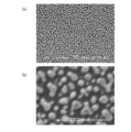
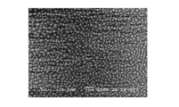
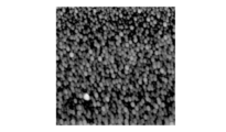
- FIG. 1 is an SEM image when the metal-based particle assembly film in the obtained metal-based particle assembly film laminated substrate is viewed from directly above.
- FIG. 1A is an enlarged image on a 10000 times scale
- FIG. 1B is an enlarged image on a 50000 times scale.
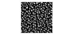
- FIG. 2 is an AFM image showing the metal-based particle assembly film in the obtained metal-based particle assembly film laminated substrate.
- VN-8010 manufactured by Keyence Corporation was used (the same applies hereinafter).
- the size of the image shown in FIG. 2 is 5 ⁇ m ⁇ 5 ⁇ m.
- the average particle diameter based on the above definition of the silver particles constituting the metal-based particle assembly of this example was determined to be 335 nm, and the average interparticle distance was 16.7 nm.
- the average height was determined to be 96.2 nm. From these, the aspect ratio (average particle diameter / average height) of the silver particles is calculated to be 3.48, and it can be seen from the acquired image that the silver particles have a flat shape. Furthermore, it can be seen from the SEM image that the metal-based particle aggregate of this example has about 6.25 ⁇ 10 10 (about 25 particles / ⁇ m 2 ) silver particles.
- Example 2 A silver nanoparticle aqueous dispersion (manufactured by Mitsubishi Paper Industries, Ltd., silver nanoparticle concentration: 25% by weight) was diluted with pure water so that the silver nanoparticle concentration was 2% by weight. Next, 1% by volume of a surfactant was added to the silver nanoparticle aqueous dispersion and stirred well, and then 80% by volume of acetone was added to the obtained silver nanoparticle aqueous dispersion at room temperature. Was sufficiently stirred to prepare a silver nanoparticle coating solution.
- the silver nanoparticle coating solution was spin-coated at 1000 rpm on a 1 mm-thick soda glass substrate whose surface was wiped with acetone, and then left for 1 minute in the atmosphere, and then in an electric furnace at 550 ° C. for 40 seconds. Baked.
- the above-mentioned silver nanoparticle coating solution is again spin-coated at 1000 rpm on the formed silver nanoparticle layer, and then left in the air for 1 minute, and then baked in an electric furnace at 550 ° C. for 40 seconds.
- a metal-based particle assembly film laminated substrate was obtained.
- FIG. 3 is an SEM image when the metal-based particle assembly film in the obtained metal-based particle assembly film laminated substrate is viewed from directly above.
- FIG. 3A is an enlarged image on a 10000 times scale
- FIG. 3B is an enlarged image on a 50000 times scale.
- FIG. 4 is an AFM image showing the metal-based particle assembly film in the obtained metal-based particle assembly film laminated substrate. The size of the image shown in FIG. 4 is 5 ⁇ m ⁇ 5 ⁇ m.
- the average particle diameter based on the above definition of the silver particles constituting the metal-based particle assembly of this example was determined to be 293 nm and the average interparticle distance was 107.8 nm.
- the average height was determined to be 93.0 nm. From these, the aspect ratio (average particle diameter / average height) of the silver particles is calculated to be 3.15, and it can be seen from the acquired image that the silver particles have a flat shape. Furthermore, it can be seen from the SEM image that the metal-based particle assembly of this example has about 3.13 ⁇ 10 10 (about 12.5 particles / ⁇ m 2 ) silver particles.
- the metal-based particle assembly film laminated substrate of Comparative Example 1 has substantially the same particle shape, aspect ratio, and average interparticle distance as Example 1 except that the average height of the metal-based particles is about 10 nm.
- the metal-based particle assembly film laminated substrate of Example 2 had substantially the same particle shape, aspect ratio, and average interparticle distance as Example 1 except that the average height of the metal-based particles was about 30 nm. .
- FIG. 5 is an absorption spectrum measured by absorptiometry of the metal-based particle assembly film laminated substrate obtained in Example 1 and Comparative Examples 1 and 2.
- Non-patent literature K. Lance Kelly, et al., "The Optical Properties of Metal Nanoparticles: The Influence of Size, Shape, and Dielectric Environment", The Journal of Physical Chemistry B, 2003, 107, 668)
- the flat silver particles as in Example 1 generally have a plasmon peak around 550 nm when the average particle size is 200 nm, and around 650 nm when the average particle size is 300 nm. (All are silver particles alone).
- the metal-based particle assembly film laminated substrate of Example 1 has a visible light region as shown in FIG. 5 even though the average particle size of silver particles constituting the metal-based particle assembly film-laminated substrate is about 300 nm (335 nm). It can be seen that the maximum wavelength of the plasmon peak on the longest wavelength side is shifted to the short wavelength side in the vicinity of about 450 nm. This phenomenon is characteristic when the silver particles are large particles having the predetermined shape as described in Example 1 and are arranged very densely at the predetermined average interparticle distance. is there. Such a phenomenon is difficult to reasonably interpret only by the presence of plasmon interaction occurring in each particle due to the proximity of the particles.
- the maximum wavelength of the plasmon peak depends on the average particle diameter of the metal-based particles.
- Comparative Examples 1 and 2 have a plasmon peak considerably longer than that of Example 1 due to the small average particle size, and the maximum wavelengths are about 510 nm and about 470 nm, respectively.
- Example 1 the absorbance at the maximum wavelength of the plasmon peak on the longest wavelength side in the visible light region is about 1.9, which is extremely higher than those in Comparative Examples 1 and 2. From this, the metal-based particles of Example 1 It can be seen that the aggregate exhibits extremely strong plasmon resonance.
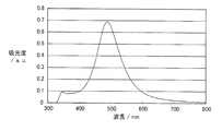
- FIG. 6 shows an absorption spectrum measured by the absorptiometry of the metal-based particle assembly film laminated substrate obtained in Example 2.
- the maximum wavelength of the plasmon peak on the longest wavelength side in the visible light region was 488 nm.
- the absorption spectra shown in FIG. 5 and FIG. 6 are from the back side of the metal-based particle assembly film laminated substrate (on the side opposite to the metal-based particle assembly film) and from the direction perpendicular to the substrate surface. It is a substrate having the same thickness and material as the substrate of the metal particle assembly film laminated substrate and the intensity I of transmitted light in all directions irradiated with incident light in the visible light region and transmitted to the metal particle assembly film side. Then, the same incident light is irradiated from the direction perpendicular to the surface of the substrate on which the metal-based particle assembly film is not stacked, and the transmitted light intensity I 0 in all directions transmitted from the opposite side of the incident surface is It was obtained by measuring using an integrating sphere spectrophotometer.
- a substrate on which a reference metal-based particle assembly was laminated was produced.
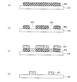
- a resist (ZEP520A, manufactured by Nippon Zeon Co., Ltd.) was spin-coated on approximately the entire surface of a soda glass substrate 100 having a length of 5 cm and a width of 5 cm (FIG. 7A).
- the thickness of the resist 400 was about 120 nm.
- a circular opening 401 was formed in the resist 400 by electron beam lithography (FIG. 7B).
- the diameter of the circular opening 401 was about 350 nm.
- the distance between the centers of the adjacent circular openings 401 was set to about 1500 nm.
- a silver film 201 was deposited on the resist 400 having the circular opening 401 by a vacuum deposition method (FIG. 7C).
- the film thickness of the silver film 201 was about 100 nm.
- the substrate having the silver film 201 is dipped in NMP (N-methyl-2-pyrrolidone, manufactured by Tokyo Chemical Industry Co., Ltd.), and left on the ultrasonic device for 1 minute at room temperature to form a film on the resist 400 and the resist 400.
- the resulting silver film 201 was peeled off, and only the silver film 201 (silver particles) in the circular opening 401 remained on the soda glass substrate 100 to obtain a reference metal-based particle assembly film laminated substrate (FIG. 7). (D)).
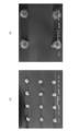
- FIG. 8 is an SEM image when the reference metal-based particle assembly film in the obtained reference metal-based particle assembly film laminated substrate is viewed from directly above.
- FIG. 8A is an enlarged image on a 20000 times scale
- FIG. 8B is an enlarged image on a 50000 times scale.
- the average particle diameter based on the above definition of the silver particles constituting the reference metal-based particle assembly film was determined to be 333 nm, and the average interparticle distance was 1264 nm.
- the average height was determined to be 105.9 nm from the separately acquired AFM image. Further, from the SEM image, it was found that the reference metal-based particle aggregate had about 62500 silver particles.
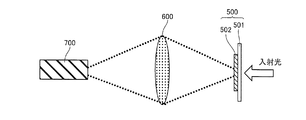
- the absorption spectrum of the metal-based particle assembly film laminated substrate of Example 1 was measured by the measurement method using the microscope objective lens (100 ⁇ ) described above. Specifically, referring to FIG. 9, the metal-based particle assembly film laminated substrate 500 is visible on the substrate 501 side (the side opposite to the metal-based particle assembly film 502) from a direction perpendicular to the substrate surface. Incident light in the light region was irradiated. Then, the transmitted light that has passed through the metal-based particle assembly film 502 side and has reached 100 times the objective lens 600 is condensed by the objective lens 600, and this condensed light is detected by the spectrophotometer 700 to obtain an absorption spectrum. Got.
- the spectrophotometer 700 was an ultraviolet-visible spectrophotometer “MCPD-3000” manufactured by Otsuka Electronics Co., Ltd., and the objective lens 600 was a “BD Plan 100 / 0.80 ELWD” manufactured by Nikon.
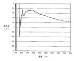
- the results are shown in FIG.
- the maximum wavelength of the plasmon peak on the longest wavelength side in the visible light region was about 450 nm as in the absorption spectrum of FIG.
- the peak maximum wavelength on the longest wavelength side in the visible light region was 654 nm. It was.
- the peak maximum wavelength on the longest wavelength side in the visible light region is blue-shifted by about 200 nm compared to the reference metal-based particle assembly film laminated substrate.
- FIG. 11 is an absorption spectrum of the metal-based particle assembly film laminated substrate of Example 2 by a measurement method using a microscope objective lens (100 ⁇ ). Since the metal-based particle aggregate of Example 2 has a larger average particle size of the metal-based particles than the metal-based particle aggregate of Comparative Example 3-1, the plasmon peak of the metal-based particle aggregate of Example 2 is Compared to Comparative Example 3-1, it appears reasonably from the Mie scattering theory that it appears on the longer wavelength side. However, actually, the plasmon peak of the metal-based particle assembly of Example 2 appeared on the short wavelength side as much as 100 nm or more as compared with Comparative Example 3-1. From this, it is reasonable that the maximum particle wavelength of the plasmon peak in Example 2 is shifted to the short wavelength side in the range of 30 to 500 nm as compared to the reference metal-based particle assembly. Is suggested.
- the metal-based particle assembly film multilayer substrate of Example 1 has an absorbance at the maximum wavelength of the peak on the longest wavelength side in the visible light region of 1.744 (FIG. 10), and the reference metal-based particle assembly film multilayer substrate. was 0.033.
- the absorbance / coverage was calculated by dividing the absorbance obtained from the absorption spectrum by the coverage of the substrate surface with metal particles, which is a parameter corresponding to the number of metal particles.
- the absorbance / coverage of the metal-based particle assembly film laminated substrate of Example 1 is 2.04 (coverage 85.3%), and the absorbance / coverage of the reference metal-based particle assembly film laminated substrate is 0.84. (Coverage 3.9%).
- Example 3-1 By growing silver particles under substantially the same conditions as in Example 1, the same metal-based particle assembly film as in Example 1 was formed on a 0.5 mm thick soda glass substrate. This metal-based particle assembly film had the same particle shape and average interparticle distance as in Example 1 except that the average height of the metal-based particles was 66.1 nm.
- a coumarin-based light emitting layer solution was spin-coated at 3000 rpm on the metal-based particle assembly film to form an extremely thin (monomolecular film scale) coumarin-based light emitting layer, thereby obtaining a light emitting device.
- a solution for a coumarin-based light emitting layer was prepared as follows. First, a coumarin dye (Exciton Coumarin 503) was dissolved in ethanol to obtain a 5 mM coumarin solution. Separately, an organic spin-on-glass (SOG) material (“OCD T-7 5500T” manufactured by Tokyo Ohka Kogyo Co., Ltd.) was diluted to 33% by volume with ethanol. The 33 volume% organic SOG material diluted solution, 5 mM coumarin solution, and ethanol were mixed so that the volume ratio was 1: 5: 5 to obtain a coumarin light emitting layer solution.
- SOG organic spin-on-glass
- Example 3-2> By growing silver particles under the same conditions as in Example 3-1, the metal-based particle assembly film described in Example 3-1 was formed on a 0.5 mm thick soda glass substrate. Immediately thereafter, the SOG solution was spin-coated on the metal-based particle assembly film, and an insulating layer having an average thickness of 10 nm was laminated. As the SOG solution, an organic SOG material “OCD T-7 5500T” manufactured by Tokyo Ohka Kogyo Co., Ltd. diluted with ethanol was used. “Average thickness” means the average thickness when formed on a metal-based particle assembly film having surface irregularities, and was measured as the thickness when the SOG solution was directly spin-coated on a soda glass substrate.
- Example 3-1 the same coumarin-based light emitting layer solution as used in Example 3-1 was spin-coated at 3000 rpm to obtain an extremely thin (monomolecular film) A coumarin-based light emitting layer was formed to obtain a light emitting device.
- Example 3-3 A light emitting device was obtained in the same manner as in Example 3-2 except that the average thickness of the insulating layer was 30 nm.
- Example 3-4> A light emitting device was obtained in the same manner as in Example 3-2 except that the average thickness of the insulating layer was 80 nm.
- Example 3-5 A light emitting device was obtained in the same manner as in Example 3-2 except that the average thickness of the insulating layer was 150 nm.
- Example 3-6 A light emitting device was obtained in the same manner as in Example 3-2 except that the average thickness of the insulating layer was 350 nm.
- ⁇ Comparative Example 3-1> A silver nanoparticle aqueous dispersion (manufactured by Mitsubishi Paper Industries, Ltd., silver nanoparticle concentration: 25 wt%) was diluted with pure water so that the silver nanoparticle concentration was 6 wt%. Next, 1% by volume of a surfactant was added to the silver nanoparticle aqueous dispersion and stirred well, and then 80% by volume of acetone was added to the obtained silver nanoparticle aqueous dispersion at room temperature. And sufficiently mixed to prepare a silver nanoparticle coating solution.
- FIG. 12 is an SEM image of the metal-based particle assembly film in the metal-based particle assembly film laminated substrate obtained in Comparative Example 3-1, viewed from directly above, and is an enlarged image of 10000 times scale.
- FIG. 13 is an AFM image showing the metal-based particle assembly film in the metal-based particle assembly film laminated substrate obtained in Comparative Example 3-1. The size of the image shown in FIG. 13 is 5 ⁇ m ⁇ 5 ⁇ m.
- the average particle diameter based on the above definition of the silver particles constituting the metal-based particle assembly of Comparative Example 3-1 was determined to be 278 nm, and the average interparticle distance was 195.5 nm.
- the average height was determined to be 99.5 nm from the AFM image shown in FIG. From these, the aspect ratio (average particle diameter / average height) of the silver particles is calculated to be 2.79, and it can be seen from the acquired image that the silver particles have a flat shape. Furthermore, it can be seen from the SEM image that the metal-based particle assembly of Comparative Example 3-1 has about 2.18 ⁇ 10 10 (about 8.72 particles / ⁇ m 2 ) silver particles.
- FIG. 14 shows an absorption spectrum of the metal-based particle assembly film laminated substrate obtained in Example 3-1 and Comparative Example 3-1 by the measurement method using the above-mentioned integrating sphere spectrophotometer.
- FIG. 15 shows an absorption spectrum of the metal-based particle assembly film-laminated substrate obtained in Comparative Example 3-1 by a measurement method using a microscope objective lens (100 ⁇ ).
- the absorbance at the maximum wavelength of the peak on the longest wavelength side in the visible light region obtained from the absorption spectrum of FIG. 15 is 0.444, and the coverage of the substrate surface with metal-based particles is 53.2%.
- Absorbance / coverage is calculated as 0.83. This absorbance / coverage is smaller than that of the reference metal-based particle assembly film laminated substrate.
- the peak wavelength of the absorption spectrum of Example 3-1 (the maximum wavelength of the plasmon peak on the longest wavelength side) is blue-shifted compared to the peak wavelength of the absorption spectrum of Comparative Example 3-1. And it turns out that the plasmon peak in the longest wavelength side sharpens, and the light absorbency in the maximum wavelength has become high.
- Example 3-1 a coumarin light emitting layer was formed on the metal particle aggregate film to obtain a light emitting device.
- Comparative Example 3-2 The metal-based particle assembly film described in Comparative Example 3-1 was formed on a 1 mm thick soda glass substrate by the same method as Comparative Example 3-1. Immediately thereafter, the SOG solution was spin-coated on the metal-based particle assembly film, and an insulating layer having an average thickness of 10 nm was laminated. As the SOG solution, an organic SOG material “OCD T-7 5500T” manufactured by Tokyo Ohka Kogyo Co., Ltd. diluted with ethanol was used.
- Example 3-2 a coumarin-based light emitting layer was formed on the outermost surface of the metal-based particle assembly film having the above insulating layer to obtain a light emitting device.
- Example 4-1 In the same manner as in Example 3-1, the metal-based particle assembly film described in Example 3-1 was formed on a 0.5 mm thick soda glass substrate.
- Alq 3 light emitting layer solution was spin-coated on the metal-based particle assembly film to form an Alq 3 light emitting layer having an average thickness of 30 nm.
- the Alq 3 light emitting layer solution was prepared by dissolving Alq 3 (Sigma-Aldrich Tris- (8-hydroxyquinoline) aluminum) in chloroform so that the concentration was 0.5 wt%.
- Example 4-2 After forming a metal-based particle assembly film having an insulating layer with an average thickness of 10 nm by the same method as in Example 3-2, an Alq 3 light emitting layer with an average thickness of 30 nm was formed by the same method as in Example 4-1. A light emitting device was obtained.
- Example 4-3 A light emitting device was obtained in the same manner as in Example 4-2, except that the average thickness of the insulating layer was 30 nm.
- Example 4-4> A light emitting device was obtained in the same manner as in Example 4-2, except that the average thickness of the insulating layer was 80 nm.
- Example 4-5 A light emitting device was obtained in the same manner as in Example 4-2, except that the average thickness of the insulating layer was 150 nm.
- Comparative Example 5-1 After the metal-based particle assembly film described in Comparative Example 3-1 was formed on a 1 mm thick soda glass substrate by the same method as Comparative Example 3-1, an average thickness of 30 nm was formed by the same method as Example 4-1. An Alq 3 light emitting layer was formed to obtain a light emitting device.
- Example 5-1 In the same manner as in Example 3-1, the metal-based particle assembly film described in Example 3-1 was formed on a 0.5 mm thick soda glass substrate.
- an F8BT light emitting layer solution was spin-coated on the metal particle aggregate film, and then baked on a hot plate at 170 ° C. for 30 minutes to form an F8BT light emitting layer having an average thickness of 30 nm.
- the solution for the F8BT light-emitting layer was prepared by dissolving F8BT (Luminescence Technology) in chlorobenzene so as to have a concentration of 1% by weight.
- Example 5-2> After forming a metal-based particle assembly film having an insulating layer with an average thickness of 10 nm by the same method as in Example 3-2, an F8BT light emitting layer with an average thickness of 30 nm was formed by the same method as in Example 5-1, A light emitting device was obtained.
- Example 5-3 A light emitting device was obtained in the same manner as in Example 5-2 except that the average thickness of the insulating layer was 30 nm.
- Comparative Example 7-1 After the metal-based particle assembly film described in Comparative Example 3-1 was formed on a 1 mm thick soda glass substrate by the same method as Comparative Example 3-1, an average thickness of 30 nm was formed by the same method as Example 5-1. A light emitting element was obtained by forming an F8BT light emitting layer.
- ⁇ Comparative Example 9-1> A conductive silver thin film having a film thickness of 13 nm was formed on a 1 mm thick soda glass substrate by vacuum deposition. The pressure in the chamber at the time of film formation was 3 ⁇ 10 ⁇ 3 Pa. Next, the substrate on which the conductive silver thin film was formed was baked for 10 minutes in an electric furnace at 400 ° C. to obtain a metal-based particle assembly film laminated substrate.
- FIG. 16 is an SEM image when the metal-based particle assembly film in the obtained metal-based particle assembly film laminated substrate is viewed from directly above.
- FIG. 16A is an enlarged image on a 10000 times scale
- FIG. 16B is an enlarged image on a 50000 times scale.
- FIG. 17 is an AFM image showing the metal-based particle assembly film in the metal-based particle assembly film laminated substrate obtained in Comparative Example 9-1. The size of the image shown in FIG. 17 is 5 ⁇ m ⁇ 5 ⁇ m.
- the average particle size based on the above definition of the silver particles constituting the metal-based particle assembly of Comparative Example 9-1 was determined to be 95 nm and the average interparticle distance was 35.2 nm.
- the average height was determined to be 29.6 nm from the AFM image shown in FIG. From these, the aspect ratio (average particle diameter / average height) of the silver particles is calculated to be 3.20.
- FIG. 18 shows the absorption spectrum of the metal-based particle assembly film laminated substrate obtained in Comparative Example 9-1 (the method for measuring the absorption spectrum is as described above).
- the peak wavelength of the absorption spectrum of Comparative Example 9-1 (the maximum wavelength of the plasmon peak on the longest wavelength side) is longer than the peak wavelength of the absorption spectrum of Example 3-1 shown in FIG. In addition, the absorbance at the peak wavelength is low.
- Example 4-1 an Alq 3 light emitting layer having an average thickness of 30 nm was formed in the same manner as in Example 4-1, to obtain a light emitting element.
- Comparative Example 9-2 The metal-based particle assembly film described in Comparative Example 9-1 was formed on a 1 mm thick soda glass substrate by the same method as Comparative Example 9-1. Immediately thereafter, the SOG solution was spin-coated on the metal-based particle assembly film, and an insulating layer having an average thickness of 10 nm was laminated. As the SOG solution, an organic SOG material “OCD T-7 5500T” manufactured by Tokyo Ohka Kogyo Co., Ltd. diluted with ethanol was used. Thereafter, an Alq 3 light emitting layer having an average thickness of 30 nm was formed by the same method as in Example 4-1, to obtain a light emitting device.
- OCD T-7 5500T manufactured by Tokyo Ohka Kogyo Co., Ltd. diluted with ethanol
- the light emitting layer 2 is formed on the light emitting layer 2 side of the photoexcited light emitting device 1.
- the photoexcited light-emitting element 1 was caused to emit light by irradiating the excitation light 3 from a direction perpendicular to the surface of the substrate.
- the excitation light source 4 a UV-LED (South Walker, UV-LED 375-nano, excitation light wavelength 375 nm) was used, and the light emitted from the excitation light source 4 was condensed by the lens 5 to be the excitation light 3, which was irradiated. .
- a wavelength cut filter 8 (sigma optical machine) that collects the light emission 6 from the optical excitation light emitting element 1 emitted in the direction of 40 ° with respect to the optical axis of the excitation light 3 by the lens 7 and cuts the light having the wavelength of the excitation light. Detection was carried out with a spectrophotometer 8 (MCPD-3000, manufactured by Otsuka Electronics Co., Ltd.) through SCF-50S-44Y manufactured by KK
- FIG. 19B is a schematic cross-sectional view showing the photoexcited light-emitting device 1 including the metal-based particle assembly film 200, the insulating layer 300, and the light-emitting layer 2 in this order on the soda glass substrate 100 manufactured in the examples and comparative examples. is there.
- the integrated value in the emission wavelength region was determined for the detected emission spectrum.
- a graph with the vertical axis is shown in FIG.
- the integrated value obtained from the emission spectrum measured for the photoexcited light emitting devices of 9-2, 9-3, 9-4, and 9-5 is divided by the integrated value obtained from the emission spectrum measured for the photoexcited light emitting device of Comparative Example 6.
- FIG. 21 shows a graph in which the obtained value is defined as “emission enhancement magnification” and this is taken as the vertical axis.
- FIG. 22 shows a graph in which the value obtained by dividing the integrated value obtained from the emission spectrum measured for the light emitting element is “emission enhancement magnification”, and this is taken as the vertical axis.
- Example 6 By growing silver particles under the same conditions as in Example 1, the metal-based particle assembly film described in Example 1 was formed on a 0.5 mm thick soda glass substrate. Immediately thereafter, a spin-on-glass (SOG) solution was spin-coated on the metal-based particle assembly film, and an insulating layer having an average thickness of 80 nm was laminated. As the SOG solution, an organic SOG material “OCD T-7 5500T” manufactured by Tokyo Ohka Kogyo Co., Ltd. diluted with ethanol was used.
- SOG organic SOG material “OCD T-7 5500T” manufactured by Tokyo Ohka Kogyo Co., Ltd. diluted with ethanol was used.
- a hole injection layer forming solution is spin-coated on the anode electrode to inject holes with an average thickness of 20 nm. Layers were laminated.
- a product obtained by diluting a product name “Plexcore AQ 1200” manufactured by PLEXTRONICS to a predetermined concentration using ethanol was used as the hole injection layer forming solution.
- the total average thickness of the insulating layer, anode electrode, and hole injection layer (that is, the average distance from the surface of the metal-based particle assembly film to the light emitting layer) is 122 nm.
- a polymer light emitter that can be dissolved in an organic solvent was dissolved in an organic solvent at a predetermined concentration, and this was spin-coated on the hole injection layer to form a light emitting layer having a thickness of 100 nm.
- an NaF layer (2 nm thickness) as an electron injection layer, an Mg layer (2 nm thickness) and an Ag layer (10 nm thickness) as a cathode electrode were laminated on the light emitting layer in this order by vacuum deposition.
- the obtained element was sealed from the surface side with a sealant (manufactured by Nagase ChemteX Corporation, UV curable resin “XNR5516ZLV”) to obtain an organic EL element.
- a constant voltage of 15 V was applied to the organic EL element of Example 6 by a source meter (source meter 2602A type manufactured by Keithley Instruments Co., Ltd.), and the element was caused to emit light with a current value flowing between the electrodes being 2.3 mA.
- the emission spectrum was measured using a spectrophotometer “CS-2000” manufactured by Konica Minolta, and the obtained emission spectrum was integrated in the visible light wavelength range to obtain the emission intensity.
- the organic current of Comparative Example 10 was the same as that of the organic EL device of Example 6 except that the value of the current flowing between the electrodes was 2.7 mA (applied voltage is 15 V as in the organic EL device of Example 6).
- the emission intensity was also determined for the EL element. As a result, it was confirmed that the organic EL element of Example 6 showed a light emission intensity of about 3.8 times that of the organic EL element of Comparative Example 10.
- Example 7 By growing silver particles under the same conditions as in Example 1, the metal-based particle assembly film described in Example 1 was formed on a 0.5 mm thick soda glass substrate. Immediately thereafter, a spin-on-glass (SOG) solution was spin-coated on the metal-based particle assembly film, and an insulating layer having an average thickness of 30 nm was laminated.
- SOG solution an organic SOG material “OCD T-7 5500T” manufactured by Tokyo Ohka Kogyo Co., Ltd. diluted with ethanol was used.
- a hole injection layer forming solution is spin-coated on the anode electrode to inject holes with an average thickness of 20 nm. Layers were laminated.
- a product obtained by diluting a product name “Plexcore AQ 1200” manufactured by PLEXTRONICS to a predetermined concentration using ethanol was used as the hole injection layer forming solution.
- the total average thickness of the insulating layer, anode electrode, and hole injection layer (that is, the average distance from the surface of the metal-based particle assembly film to the light emitting layer) is 72 nm.
- an Alq 3 film having a thickness of 80 nm was formed as a light emitting layer on the hole injection layer by vacuum deposition. Thereafter, an NaF layer (2 nm thickness) as an electron injection layer, an Mg layer (2 nm thickness) and an Ag layer (10 nm thickness) as a cathode electrode were laminated on the light emitting layer in this order by vacuum deposition.
- the obtained element was sealed from the surface side using a sealing agent (UV curable resin “XNR5516ZLV” manufactured by Nagase ChemteX Corporation) to obtain an organic EL element.
- a constant voltage of 11 V was applied to the organic EL element of Example 7 by a source meter (source meter 2602A type manufactured by Keithley Instruments Co., Ltd.), and the element was caused to emit light with a current value flowing between the electrodes being 0.7 mA.
- the emission spectrum was measured using a spectrophotometer “CS-2000” manufactured by Konica Minolta, and the obtained emission spectrum was integrated in the visible light wavelength range to obtain the emission intensity.
- the value of the current flowing between the electrodes was adjusted to 1.1 mA (applied voltage is 11 V as in the organic EL element of Example 7), The emission intensity was also determined for the organic EL element. As a result, it was confirmed that the organic EL device of Example 7 had a light emission intensity about 2.6 times that of the organic EL device of Comparative Example 11.
Landscapes
- Physics & Mathematics (AREA)
- Optics & Photonics (AREA)
- Nanotechnology (AREA)
- Chemical & Material Sciences (AREA)
- Engineering & Computer Science (AREA)
- Life Sciences & Earth Sciences (AREA)
- General Physics & Mathematics (AREA)
- Crystallography & Structural Chemistry (AREA)
- Biophysics (AREA)
- Electroluminescent Light Sources (AREA)
- Led Device Packages (AREA)
- Photovoltaic Devices (AREA)
- Sustainable Development (AREA)
- Investigating Or Analysing Materials By Optical Means (AREA)
- Optical Filters (AREA)
Abstract
Description
[1] 30個以上の金属系粒子が互いに離間して二次元的に配置されてなる粒子集合体であって、
前記金属系粒子は、その平均粒径が200~1600nmの範囲内、平均高さが55~500nmの範囲内、前記平均高さに対する前記平均粒径の比で定義されるアスペクト比が1~8の範囲内にあり、
可視光領域における吸光スペクトルにおいて、前記平均粒径と同じ粒径、前記平均高さと同じ高さおよび同じ材質からなる金属系粒子を、金属系粒子間の距離がすべて1~2μmの範囲内となるように配置した参照金属系粒子集合体よりも、同じ金属系粒子数での比較において、最も長波長側にあるピークの極大波長における吸光度が高い金属系粒子集合体。
本発明の金属系粒子集合体は、30個以上の金属系粒子が互いに離間して二次元的に配置されてなる粒子集合体である。該集合体を構成する金属系粒子は、その平均粒径が200~1600nmの範囲内、平均高さが55~500nmの範囲内、平均高さに対する平均粒径の比で定義されるアスペクト比が1~8の範囲内とされる。本発明の金属系粒子集合体は、可視光領域における吸光スペクトルにおいて、それが有する平均粒径と同じ粒径、それが有する平均高さと同じ高さおよび同じ材質からなる金属系粒子を、金属系粒子間の距離がすべて1~2μmの範囲内となるように配置した参照金属系粒子集合体よりも、同じ金属系粒子数での比較において、最も長波長側にあるピークの極大波長における吸光度が高い。また、本発明の金属系粒子集合体膜積層基板は、上記金属系粒子集合体を基板上に積層(担持)させてなるものである。
吸光度=-log10(I/I0)
で表される。
本発明のプラズモン材料(金属系粒子集合体および金属系粒子集合体膜積層基板)は、次のような方法によって作製することができる。
(2)所定の形状を有する金属系粒子を所定の厚みを有する両親媒性材料からなる保護層で被覆した後、LB(Langmuir Blodgett)膜法により、これを基板上にフィルム化する方法、
(3)その他、蒸着またはスパッタリングにより作製した薄膜を後処理する方法、レジスト加工、エッチング加工、金属系粒子が分散された分散液を用いたキャスト法など。
金属系粒子の平均高さ/金属系粒子成長時間(金属系材料の供給時間)
で定義される。「金属系粒子の平均高さ」の定義は上述のとおりである。
金属系粒子の平均粒径/金属系粒子成長時間(金属系材料の供給時間)
で定義される。「金属系粒子の平均粒径」の定義は上述のとおりである。
<実施例1>
直流マグネトロンスパッタリング装置を用いて、下記の条件で、ソーダガラス基板上に、銀粒子を極めてゆっくりと成長させ、基板表面の全面に金属系粒子集合体の薄膜を形成して、金属系粒子集合体層積層基板を得た。
チャンバ内圧力(スパッタガス圧):10Pa、
基板・ターゲット間距離:100mm、
スパッタ電力:4W、
平均粒径成長速度(平均粒径/スパッタ時間):0.9nm/分、
平均高さ成長速度(=平均堆積速度=平均高さ/スパッタ時間):0.25nm/分、
基板温度:300℃、
基板サイズおよび形状:一辺が5cmの正方形。
銀ナノ粒子水分散物(三菱製紙社製、銀ナノ粒子濃度:25重量%)を純水で、銀ナノ粒子濃度が2重量%となるように希釈した。次いで、この銀ナノ粒子水分散物に対して1体積%の界面活性剤を添加して良く攪拌した後、得られた銀ナノ粒子水分散物に対して80体積%のアセトンを添加して常温で十分撹拌し、銀ナノ粒子塗工液を調製した。
直流マグネトロンスパッタリング法における堆積時間を変更することにより、比較例1および2の金属系粒子集合体膜積層基板を得た。比較例1の金属系粒子集合体膜積層基板は、金属系粒子の平均高さが約10nmであること以外は実施例1と略同じ粒子形状、アスペクト比および平均粒子間距離を有し、比較例2の金属系粒子集合体膜積層基板は、金属系粒子の平均高さが約30nmであること以外は実施例1と略同じ粒子形状、アスペクト比および平均粒子間距離を有するものであった。
図5は、実施例1および比較例1~2で得られた金属系粒子集合体膜積層基板の吸光光度法により測定された吸光スペクトルである。非特許文献(K. Lance Kelly, et al., "The Optical Properties of Metal Nanoparticles: The Influence of Size, Shape, and Dielectric Environment", The Journal of Physical Chemistry B, 2003, 107, 668)に示されているように、実施例1のような扁平形状の銀粒子は、平均粒径が200nmのとき約550nm付近に、平均粒径が300nmのときは650nm付近にプラズモンピークを持つことが一般的である(いずれも銀粒子単独の場合である)。
吸光度=-log10(I/I0)
で表される。
図7に示される方法に従って、参照金属系粒子集合体が積層された基板を作製した。まず、縦5cm、横5cmのソーダガラス基板100のおよそ全面にレジスト(日本ゼオン株式会社製 ZEP520A)をスピンコートした(図7(a))。レジスト400の厚みは約120nmとした。次に、電子ビームリソグラフィーによってレジスト400に円形開口401を形成した(図7(b))。円形開口401の直径は約350nmとした。また、隣り合う円形開口401の中心間距離は約1500nmとした。
<実施例3-1>
実施例1とほぼ同じ条件で銀粒子を成長させることにより、0.5mm厚のソーダガラス基板上に実施例1と同様の金属系粒子集合体膜を形成した。この金属系粒子集合体膜は、金属系粒子の平均高さが66.1nmであること以外は実施例1と同じ粒子形状および平均粒子間距離を有するものであった。
実施例3-1と同条件で銀粒子を成長させることにより、0.5mm厚のソーダガラス基板上に実施例3-1に記載の金属系粒子集合体膜を形成した。その後直ちに、SOG溶液を金属系粒子集合体膜上にスピンコートして、平均厚み10nmの絶縁層を積層した。SOG溶液には、有機系SOG材料である東京応化工業株式会社製「OCD T-7 5500T」をエタノールで希釈したものを用いた。「平均厚み」とは、表面凹凸を有する金属系粒子集合体膜上に形成されたときの平均厚みを意味しており、SOG溶液をソーダガラス基板上に直接スピンコートしたときの厚みとして測定した(以下の実施例、比較例についても同様)。平均厚みが比較的小さい値のときは金属系粒子集合体膜の谷部分にのみ絶縁層が形成され、金属系粒子集合体膜の最表面全体を被覆できないことがある。
絶縁層の平均厚みを30nmとしたこと以外は実施例3-2と同様にして、発光素子を得た。
絶縁層の平均厚みを80nmとしたこと以外は実施例3-2と同様にして、発光素子を得た。
絶縁層の平均厚みを150nmとしたこと以外は実施例3-2と同様にして、発光素子を得た。
絶縁層の平均厚みを350nmとしたこと以外は実施例3-2と同様にして、発光素子を得た。
銀ナノ粒子水分散物(三菱製紙社製、銀ナノ粒子濃度:25重量%)を純水で、銀ナノ粒子濃度が6重量%となるように希釈した。次いで、この銀ナノ粒子水分散物に対して1体積%の界面活性剤を添加して良く攪拌した後、得られた銀ナノ粒子水分散物に対して80体積%のアセトンを添加して常温で十分振り混ぜ、銀ナノ粒子塗工液を調製した。
比較例3-1と同じ方法で、1mm厚のソーダガラス基板上に比較例3-1に記載の金属系粒子集合体膜を形成した。その後直ちに、SOG溶液を金属系粒子集合体膜上にスピンコートして、平均厚み10nmの絶縁層を積層した。SOG溶液には、有機系SOG材料である東京応化工業株式会社製「OCD T-7 5500T」をエタノールで希釈したものを用いた。
絶縁層の平均厚みを30nmとしたこと以外は比較例3-2と同様にして、発光素子を得た。
絶縁層の平均厚みを80nmとしたこと以外は比較例3-2と同様にして、発光素子を得た。
絶縁層の平均厚みを150nmとしたこと以外は比較例3-2と同様にして、発光素子を得た。
絶縁層の平均厚みを350nmとしたこと以外は比較例3-2と同様にして、発光素子を得た。
金属系粒子集合体膜を形成しないこと以外は実施例3-1と同様にして発光素子を得た。
実施例3-1と同じ方法で、0.5mm厚のソーダガラス基板上に実施例3-1に記載の金属系粒子集合体膜を形成した。
実施例3-2と同じ方法で、平均厚み10nmの絶縁層を有する金属系粒子集合体膜を形成した後、実施例4-1と同じ方法で平均厚み30nmのAlq3発光層を形成して、発光素子を得た。
絶縁層の平均厚みを30nmとしたこと以外は実施例4-2と同様にして、発光素子を得た。
絶縁層の平均厚みを80nmとしたこと以外は実施例4-2と同様にして、発光素子を得た。
絶縁層の平均厚みを150nmとしたこと以外は実施例4-2と同様にして、発光素子を得た。
比較例3-1と同じ方法で、1mm厚のソーダガラス基板上に比較例3-1に記載の金属系粒子集合体膜を形成した後、実施例4-1と同じ方法で平均厚み30nmのAlq3発光層を形成して、発光素子を得た。
比較例3-2と同じ方法で、平均厚み10nmの絶縁層を有する金属系粒子集合体膜を形成した後、実施例4-1と同じ方法で平均厚み30nmのAlq3発光層を形成して、発光素子を得た。
絶縁層の平均厚みを30nmとしたこと以外は比較例5-2と同様にして、発光素子を得た。
絶縁層の平均厚みを80nmとしたこと以外は比較例5-2と同様にして、発光素子を得た。
絶縁層の平均厚みを150nmとしたこと以外は比較例5-2と同様にして、発光素子を得た。
金属系粒子集合体膜を形成しないこと以外は実施例4-1と同様にして発光素子を得た。
実施例3-1と同じ方法で、0.5mm厚のソーダガラス基板上に実施例3-1に記載の金属系粒子集合体膜を形成した。
実施例3-2と同じ方法で、平均厚み10nmの絶縁層を有する金属系粒子集合体膜を形成した後、実施例5-1と同じ方法で平均厚み30nmのF8BT発光層を形成して、発光素子を得た。
絶縁層の平均厚みを30nmとしたこと以外は実施例5-2と同様にして、発光素子を得た。
比較例3-1と同じ方法で、1mm厚のソーダガラス基板上に比較例3-1に記載の金属系粒子集合体膜を形成した後、実施例5-1と同じ方法で平均厚み30nmのF8BT発光層を形成して、発光素子を得た。
比較例3-2と同じ方法で、平均厚み10nmの絶縁層を有する金属系粒子集合体膜積層基板を形成した後、実施例5-1と同じ方法で平均厚み30nmのF8BT発光層を形成して、発光素子を得た。
絶縁層の平均厚みを30nmとしたこと以外は比較例7-2と同様にして、発光素子を得た。
金属系粒子集合体膜を形成しないこと以外は実施例5-1と同様にして発光素子を得た。
1mm厚のソーダガラス基板上に、真空蒸着法によって膜厚13nmの導電性銀薄膜を成膜した。成膜の際のチャンバ内圧力は3×10⁻³Paとした。次に、導電性銀薄膜が成膜された基板を400℃の電気炉内で10分間焼成し、金属系粒子集合体膜積層基板を得た。
比較例9-1と同じ方法で、1mm厚のソーダガラス基板上に比較例9-1に記載の金属系粒子集合体膜を形成した。その後直ちに、SOG溶液を金属系粒子集合体膜上にスピンコートして、平均厚み10nmの絶縁層を積層した。SOG溶液には、有機系SOG材料である東京応化工業株式会社製「OCD T-7 5500T」をエタノールで希釈したものを用いた。その後、実施例4-1と同じ方法で平均厚み30nmのAlq3発光層を形成して、発光素子を得た。
絶縁層の平均厚みを30nmとしたこと以外は比較例9-2と同様にして、発光素子を得た。
絶縁層の平均厚みを80nmとしたこと以外は比較例9-2と同様にして、発光素子を得た。
絶縁層の平均厚みを150nmとしたこと以外は比較例9-2と同様にして、発光素子を得た。
<実施例6>
実施例1と同条件で銀粒子を成長させることにより、0.5mm厚のソーダガラス基板上に実施例1に記載の金属系粒子集合体膜を形成した。その後直ちに、スピンオングラス(SOG)溶液を金属系粒子集合体膜上にスピンコートして、平均厚み80nmの絶縁層を積層した。SOG溶液には、有機系SOG材料である東京応化工業株式会社製「OCD T-7 5500T」をエタノールで希釈したものを用いた。
金属系粒子集合体膜を形成しないこと以外は実施例6と同様にして有機EL素子を作製した。
実施例1と同条件で銀粒子を成長させることにより、0.5mm厚のソーダガラス基板上に実施例1に記載の金属系粒子集合体膜を形成した。その後直ちに、スピンオングラス(SOG)溶液を金属系粒子集合体膜上にスピンコートして、平均厚み30nmの絶縁層を積層した。SOG溶液には、有機系SOG材料である東京応化工業株式会社製「OCD T-7 5500T」をエタノールで希釈したものを用いた。
金属系粒子集合体膜を形成しないこと以外は実施例7と同様にして有機EL素子を作製した。
Claims (10)
- 30個以上の金属系粒子が互いに離間して二次元的に配置されてなる粒子集合体であって、
前記金属系粒子は、その平均粒径が200~1600nmの範囲内、平均高さが55~500nmの範囲内、前記平均高さに対する前記平均粒径の比で定義されるアスペクト比が1~8の範囲内にあり、
可視光領域における吸光スペクトルにおいて、前記平均粒径と同じ粒径、前記平均高さと同じ高さおよび同じ材質からなる金属系粒子を、金属系粒子間の距離がすべて1~2μmの範囲内となるように配置した参照金属系粒子集合体よりも、同じ金属系粒子数での比較において、最も長波長側にあるピークの極大波長における吸光度が高い金属系粒子集合体。 - 金属系粒子集合体を構成する前記金属系粒子は、前記アスペクト比が1を超える扁平状の粒子である請求項1に記載の金属系粒子集合体。
- 金属系粒子集合体を構成する前記金属系粒子は、銀からなる請求項1に記載の金属系粒子集合体。
- 金属系粒子集合体を構成する前記金属系粒子は、その隣り合う金属系粒子との間に関して非導電性である請求項1に記載の金属系粒子集合体。
- 基板と、前記基板上に積層される請求項1に記載の金属系粒子集合体からなる膜とを備える金属系粒子集合体膜積層基板。
- 可視光領域における吸光スペクトルにおいて、最も長波長側にあるピークが350~550nmの範囲内に極大波長を有する請求項5に記載の金属系粒子集合体膜積層基板。
- 可視光領域における吸光スペクトルにおいて、最も長波長側にあるピークの極大波長における吸光度が1以上である請求項5に記載の金属系粒子集合体膜積層基板。
- 前記膜を構成するそれぞれの金属系粒子の表面を覆う絶縁層をさらに備える請求項5に記載の金属系粒子集合体膜積層基板。
- 10nm以上の厚みを有する光吸収層と、請求項1に記載の金属系粒子集合体または請求項5に記載の金属系粒子集合体膜積層基板とを備える光学素子。
- 10nm以上の厚みを有する発光層と、請求項1に記載の金属系粒子集合体または請求項5に記載の金属系粒子集合体膜積層基板とを備える光学素子。
Priority Applications (4)
| Application Number | Priority Date | Filing Date | Title |
|---|---|---|---|
| KR1020137027886A KR102086862B1 (ko) | 2011-03-31 | 2012-03-30 | 금속계 입자 집합체 |
| EP12764351.8A EP2693845A4 (en) | 2011-03-31 | 2012-03-30 | METAL PARTICLE ARRANGEMENT |
| US14/007,504 US9696462B2 (en) | 2011-03-31 | 2012-03-30 | Metal-based particle assembly |
| CN201280015771.7A CN103460806B (zh) | 2011-03-31 | 2012-03-30 | 金属系颗粒集合体 |
Applications Claiming Priority (6)
| Application Number | Priority Date | Filing Date | Title |
|---|---|---|---|
| JP2011079476 | 2011-03-31 | ||
| JP2011-079476 | 2011-03-31 | ||
| JP2011-245337 | 2011-11-09 | ||
| JP2011245337 | 2011-11-09 | ||
| JP2012018647 | 2012-01-31 | ||
| JP2012-018647 | 2012-01-31 |
Publications (1)
| Publication Number | Publication Date |
|---|---|
| WO2012133778A1 true WO2012133778A1 (ja) | 2012-10-04 |
Family
ID=46931473
Family Applications (1)
| Application Number | Title | Priority Date | Filing Date |
|---|---|---|---|
| PCT/JP2012/058599 Ceased WO2012133778A1 (ja) | 2011-03-31 | 2012-03-30 | 金属系粒子集合体 |
Country Status (7)
| Country | Link |
|---|---|
| US (1) | US9696462B2 (ja) |
| EP (1) | EP2693845A4 (ja) |
| JP (1) | JP6085095B2 (ja) |
| KR (1) | KR102086862B1 (ja) |
| CN (1) | CN103460806B (ja) |
| TW (1) | TWI618924B (ja) |
| WO (1) | WO2012133778A1 (ja) |
Cited By (9)
| Publication number | Priority date | Publication date | Assignee | Title |
|---|---|---|---|---|
| WO2013061881A1 (ja) * | 2011-10-26 | 2013-05-02 | 住友化学株式会社 | 光電変換素子 |
| WO2013146268A1 (ja) * | 2012-03-27 | 2013-10-03 | 住友化学株式会社 | 無機層発光素子 |
| JP2014058730A (ja) * | 2012-09-19 | 2014-04-03 | Sumitomo Chemical Co Ltd | 金属系粒子集合体の製造方法 |
| JP2015531167A (ja) * | 2013-05-23 | 2015-10-29 | サムスン トータル ペトロケミカルズ カンパニー リミテッド | 異方性金属ナノ粒子を利用した発光効率が増大された光変換発光素子 |
| US9257662B2 (en) | 2011-10-03 | 2016-02-09 | Sumitomo Chemical Company, Limited | Quantum dot light-emitting device |
| JP2016507893A (ja) * | 2012-12-21 | 2016-03-10 | ベネルギー エルエルシー | 太陽エネルギーを収集して変換するための、装置、システム及び方法 |
| US9693423B2 (en) | 2011-03-31 | 2017-06-27 | Sumitomo Chemical Company, Limited | Metal-based particle assembly |
| US9693424B2 (en) | 2011-03-31 | 2017-06-27 | Sumitomo Chemical Company, Limited | Metal-based particle assembly |
| US9696462B2 (en) | 2011-03-31 | 2017-07-04 | Sumitomo Chemical Company, Limited | Metal-based particle assembly |
Families Citing this family (7)
| Publication number | Priority date | Publication date | Assignee | Title |
|---|---|---|---|---|
| JP5979932B2 (ja) * | 2011-03-31 | 2016-08-31 | 住友化学株式会社 | 有機エレクトロルミネッセンス素子 |
| JP6018857B2 (ja) * | 2012-09-18 | 2016-11-02 | 住友化学株式会社 | 金属系粒子集合体 |
| TWI472059B (zh) * | 2013-10-09 | 2015-02-01 | Cheng Sheng Tsung | A method of forming a surface plasma using a microstructure |
| US20170241009A1 (en) * | 2016-02-24 | 2017-08-24 | Guardian Industries Corp. | Coated article including metal island layer(s) formed using stoichiometry control, and/or method of making the same |
| US10562812B2 (en) | 2018-06-12 | 2020-02-18 | Guardian Glass, LLC | Coated article having metamaterial-inclusive layer, coating having metamaterial-inclusive layer, and/or method of making the same |
| US10830933B2 (en) | 2018-06-12 | 2020-11-10 | Guardian Glass, LLC | Matrix-embedded metamaterial coating, coated article having matrix-embedded metamaterial coating, and/or method of making the same |
| CN111710766A (zh) * | 2020-06-19 | 2020-09-25 | 中国工程物理研究院电子工程研究所 | 一种具有折射率可调的复合增透膜的可见光led芯片 |
Citations (8)
| Publication number | Priority date | Publication date | Assignee | Title |
|---|---|---|---|---|
| JPH08271431A (ja) | 1995-03-17 | 1996-10-18 | Avl Medical Instr Ag | 光化学蛍光センサー及びその測定方法 |
| WO2005033335A2 (fr) | 2003-10-09 | 2005-04-14 | Commissariat A L'energie Atomique | Micro-capteurs et nano-capteurs d’especes chimiques et biologiques a plasmons de surface |
| JP2007017432A (ja) * | 2005-06-08 | 2007-01-25 | Canon Inc | プラズモン共鳴を利用して検体中の標的物質を検知するための検知装置に用いられる検知素子及びその製造方法 |
| JP2007501391A (ja) * | 2003-08-06 | 2007-01-25 | ユニバーシティー オブ ピッツバーグ | 表面プラズモンを増強するナノ光学素子及びこの製造方法 |
| JP2007139540A (ja) | 2005-11-17 | 2007-06-07 | Kyoto Univ | 蛍光増強素子、蛍光素子、及び蛍光増強方法 |
| WO2008082569A1 (en) * | 2006-12-29 | 2008-07-10 | Nanolambda, Inc. | Wavelength selective metallic embossing nanostructure |
| JP2009074947A (ja) * | 2007-09-21 | 2009-04-09 | Hitachi High-Technologies Corp | 標的物質を検出するための分析装置、又は分析方法、若しくはこれら分析装置及び分析方法に用いるデバイス |
| WO2011027830A1 (ja) * | 2009-09-07 | 2011-03-10 | 国立大学法人北海道大学 | 光電変換装置、光検出装置、及び光検出方法 |
Family Cites Families (45)
| Publication number | Priority date | Publication date | Assignee | Title |
|---|---|---|---|---|
| US6074575A (en) | 1994-11-14 | 2000-06-13 | Mitsui Mining & Smelting Co., Ltd. | Thin film electro-luminescence device |
| JPH08134440A (ja) | 1994-11-14 | 1996-05-28 | Mitsui Mining & Smelting Co Ltd | 薄膜エレクトロルミネッセンス素子 |
| TW527848B (en) | 2000-10-25 | 2003-04-11 | Matsushita Electric Industrial Co Ltd | Light-emitting element and display device and lighting device utilizing thereof |
| US7335835B2 (en) | 2002-11-08 | 2008-02-26 | The Boeing Company | Solar cell structure with by-pass diode and wrapped front-side diode interconnection |
| TW595259B (en) | 2003-01-28 | 2004-06-21 | Ind Tech Res Inst | Organic electroluminescent device |
| CN1527648A (zh) | 2003-03-07 | 2004-09-08 | 财团法人工业技术研究院 | 有机电激发光装置 |
| US7420156B2 (en) | 2003-08-06 | 2008-09-02 | University Of Pittsburgh | Metal nanowire based bandpass filter arrays in the optical frequency range |
| US7704754B2 (en) | 2004-01-27 | 2010-04-27 | American Environmental Systems, Inc. | Method of plasmon-enhanced properties of materials and applications thereof |
| US20070295381A1 (en) | 2004-03-29 | 2007-12-27 | Kyocera Corporation | Solar Cell Module and Photovoltaic Power Generator Using This |
| US8592680B2 (en) | 2004-08-11 | 2013-11-26 | The Trustees Of Princeton University | Organic photosensitive devices |
| WO2006085515A1 (ja) | 2005-02-09 | 2006-08-17 | Kyoto University | 反射率制御光学素子及び超薄膜光吸収増強素子 |
| US7811679B2 (en) | 2005-05-20 | 2010-10-12 | Lg Display Co., Ltd. | Display devices with light absorbing metal nanoparticle layers |
| US7403287B2 (en) | 2005-06-08 | 2008-07-22 | Canon Kabushiki Kaisha | Sensing element used in sensing device for sensing target substance in specimen by using plasmon resonance |
| FR2891279B1 (fr) | 2005-09-27 | 2007-12-14 | Centre Nat Rech Scient | Nouvelles puces pour la detection par le plasmon de surface (spr) |
| JP2007165284A (ja) * | 2005-11-18 | 2007-06-28 | Seiko Instruments Inc | エレクトロルミネッセンス素子及びこれを用いた表示装置 |
| EP1998386B1 (en) | 2006-03-20 | 2015-02-25 | Panasonic Corporation | Organic thin film solar cell |
| JP2007335222A (ja) | 2006-06-15 | 2007-12-27 | Ipb:Kk | 光電極、及びそれを用いた色素増感太陽電池、並びにその製造方法 |
| US20100022020A1 (en) | 2006-09-01 | 2010-01-28 | Halas Nancy J | Compositions for surface enhanced infrared absorption spectra and methods of using same |
| JP4250651B2 (ja) | 2006-09-28 | 2009-04-08 | 株式会社東芝 | 粒子配列方法、及び、発光素子の製造方法 |
| WO2008068758A1 (en) | 2006-12-05 | 2008-06-12 | Yeda Research And Development Company Ltd. | Device and method for optical localized plasmon sensing |
| JP2008214363A (ja) | 2007-02-28 | 2008-09-18 | Canon Inc | ナノ粒子発光材料、これを用いた電界発光素子及びインク組成物、並びに表示装置 |
| JP2008243669A (ja) | 2007-03-28 | 2008-10-09 | Toyota Central R&D Labs Inc | 有機電界発光素子 |
| US20080278063A1 (en) | 2007-05-07 | 2008-11-13 | Cok Ronald S | Electroluminescent device having improved power distribution |
| JP5300344B2 (ja) | 2007-07-06 | 2013-09-25 | キヤノン株式会社 | 光検出素子及び撮像素子、光検出方法及び撮像方法 |
| EP2203030A4 (en) | 2007-08-27 | 2010-09-29 | Panasonic Elec Works Co Ltd | ORGANIC EL LIGHT ELEMENT |
| DE102007053712A1 (de) * | 2007-11-10 | 2009-05-14 | Oerlikon Accotex Texparts Gmbh | Oberwalzen-Trag- und Belastungsarm |
| US8115920B2 (en) | 2007-11-14 | 2012-02-14 | 3M Innovative Properties Company | Method of making microarrays |
| US8097295B2 (en) | 2008-02-27 | 2012-01-17 | The University Of Utah Research Foundation | Method of making nanoparticles by electroless plating |
| JP5362711B2 (ja) | 2008-05-21 | 2013-12-11 | パイオニア株式会社 | 有機発光素子 |
| US8058609B2 (en) | 2008-09-30 | 2011-11-15 | The Invention Science Fund I, Llc | Beam power with multipoint broadcast |
| JP2010123675A (ja) * | 2008-11-18 | 2010-06-03 | Fuji Electric Holdings Co Ltd | 薄膜太陽電池及び薄膜太陽電池の製造方法 |
| US20100126567A1 (en) | 2008-11-21 | 2010-05-27 | Lightwave Power, Inc. | Surface plasmon energy conversion device |
| KR100970265B1 (ko) * | 2008-12-15 | 2010-07-16 | 한국기계연구원 | 표면 플라즈몬 공명 구조를 갖는 유기 발광 표시장치 및 이의 제조 방법 |
| US9013689B2 (en) | 2009-01-09 | 2015-04-21 | Trustees Of Boston University | Engineered SERS substrates employing nanoparticle cluster arrays with multiscale signal enhancement |
| JP5266092B2 (ja) | 2009-02-24 | 2013-08-21 | パナソニック株式会社 | 発光素子 |
| JP5312146B2 (ja) | 2009-03-30 | 2013-10-09 | ユー・ディー・シー アイルランド リミテッド | 発光素子 |
| JP5312145B2 (ja) | 2009-03-30 | 2013-10-09 | ユー・ディー・シー アイルランド リミテッド | エレクトロルミネッセンス素子 |
| US8259381B2 (en) * | 2009-06-05 | 2012-09-04 | Exelis Inc. | Phase-change materials and optical limiting devices utilizing phase-change materials |
| WO2011125101A1 (ja) | 2010-04-02 | 2011-10-13 | 株式会社 東芝 | 光電変換素子及びその製造方法 |
| JP2012074569A (ja) | 2010-09-29 | 2012-04-12 | Jx Nippon Oil & Energy Corp | 光電変換素子 |
| JP6125758B2 (ja) | 2011-03-31 | 2017-05-10 | 住友化学株式会社 | 光学素子 |
| JP6018774B2 (ja) * | 2011-03-31 | 2016-11-02 | 住友化学株式会社 | 金属系粒子集合体 |
| JP5979932B2 (ja) | 2011-03-31 | 2016-08-31 | 住友化学株式会社 | 有機エレクトロルミネッセンス素子 |
| JP6085095B2 (ja) | 2011-03-31 | 2017-02-22 | 住友化学株式会社 | 光学素子 |
| JP6373552B2 (ja) | 2011-10-26 | 2018-08-15 | 住友化学株式会社 | 光電変換素子 |
-
2012
- 2012-03-27 JP JP2012071679A patent/JP6085095B2/ja active Active
- 2012-03-30 US US14/007,504 patent/US9696462B2/en active Active
- 2012-03-30 WO PCT/JP2012/058599 patent/WO2012133778A1/ja not_active Ceased
- 2012-03-30 EP EP12764351.8A patent/EP2693845A4/en not_active Withdrawn
- 2012-03-30 KR KR1020137027886A patent/KR102086862B1/ko active Active
- 2012-03-30 TW TW101111527A patent/TWI618924B/zh active
- 2012-03-30 CN CN201280015771.7A patent/CN103460806B/zh active Active
Patent Citations (8)
| Publication number | Priority date | Publication date | Assignee | Title |
|---|---|---|---|---|
| JPH08271431A (ja) | 1995-03-17 | 1996-10-18 | Avl Medical Instr Ag | 光化学蛍光センサー及びその測定方法 |
| JP2007501391A (ja) * | 2003-08-06 | 2007-01-25 | ユニバーシティー オブ ピッツバーグ | 表面プラズモンを増強するナノ光学素子及びこの製造方法 |
| WO2005033335A2 (fr) | 2003-10-09 | 2005-04-14 | Commissariat A L'energie Atomique | Micro-capteurs et nano-capteurs d’especes chimiques et biologiques a plasmons de surface |
| JP2007017432A (ja) * | 2005-06-08 | 2007-01-25 | Canon Inc | プラズモン共鳴を利用して検体中の標的物質を検知するための検知装置に用いられる検知素子及びその製造方法 |
| JP2007139540A (ja) | 2005-11-17 | 2007-06-07 | Kyoto Univ | 蛍光増強素子、蛍光素子、及び蛍光増強方法 |
| WO2008082569A1 (en) * | 2006-12-29 | 2008-07-10 | Nanolambda, Inc. | Wavelength selective metallic embossing nanostructure |
| JP2009074947A (ja) * | 2007-09-21 | 2009-04-09 | Hitachi High-Technologies Corp | 標的物質を検出するための分析装置、又は分析方法、若しくはこれら分析装置及び分析方法に用いるデバイス |
| WO2011027830A1 (ja) * | 2009-09-07 | 2011-03-10 | 国立大学法人北海道大学 | 光電変換装置、光検出装置、及び光検出方法 |
Non-Patent Citations (4)
| Title |
|---|
| "Particle Measurement Technique", 1994, NIKKAN KOGYO SHIMBUN, LTD., pages: 5 |
| K. LANCE KELLY ET AL.: "The Optical Properties of Metal Nanoparticles: The Influence of Size, Shape, and Dielectric Environment", THE JOURNAL OF PHYSICAL CHEMISTRY B, vol. 107, 2003, pages 668, XP055034185, DOI: doi:10.1021/jp026731y |
| See also references of EP2693845A4 |
| T. FUKUURA; M. KAWASAKI: "Long Range Enhancement of Molecular Fluorescence by Closely Packed Submicro-scale Ag Islands", E-JOURNAL OF SURFACE SCIENCE AND NANOTECHNOLOGY, vol. 7, 2009, pages 653 |
Cited By (13)
| Publication number | Priority date | Publication date | Assignee | Title |
|---|---|---|---|---|
| US10379267B2 (en) | 2011-03-31 | 2019-08-13 | Sumitomo Chemical Company, Limited | Metal-based particle assembly |
| US9696462B2 (en) | 2011-03-31 | 2017-07-04 | Sumitomo Chemical Company, Limited | Metal-based particle assembly |
| US9693424B2 (en) | 2011-03-31 | 2017-06-27 | Sumitomo Chemical Company, Limited | Metal-based particle assembly |
| US9693423B2 (en) | 2011-03-31 | 2017-06-27 | Sumitomo Chemical Company, Limited | Metal-based particle assembly |
| US9257662B2 (en) | 2011-10-03 | 2016-02-09 | Sumitomo Chemical Company, Limited | Quantum dot light-emitting device |
| EP2772945A4 (en) * | 2011-10-26 | 2015-09-09 | Sumitomo Chemical Co | PHOTOELECTRIC CONVERSION ELEMENT |
| WO2013061881A1 (ja) * | 2011-10-26 | 2013-05-02 | 住友化学株式会社 | 光電変換素子 |
| US9263630B2 (en) | 2012-03-27 | 2016-02-16 | Sumitomo Chemical Company, Limited | Inorganic layer light-emitting device |
| WO2013146268A1 (ja) * | 2012-03-27 | 2013-10-03 | 住友化学株式会社 | 無機層発光素子 |
| JP2014058730A (ja) * | 2012-09-19 | 2014-04-03 | Sumitomo Chemical Co Ltd | 金属系粒子集合体の製造方法 |
| JP2016507893A (ja) * | 2012-12-21 | 2016-03-10 | ベネルギー エルエルシー | 太陽エネルギーを収集して変換するための、装置、システム及び方法 |
| JP2015531167A (ja) * | 2013-05-23 | 2015-10-29 | サムスン トータル ペトロケミカルズ カンパニー リミテッド | 異方性金属ナノ粒子を利用した発光効率が増大された光変換発光素子 |
| GB2517883B (en) * | 2013-05-23 | 2018-10-10 | Hanwha Total Petrochemical Co Ltd | Light conversion light-emitting device with enhanced luminescence efficiency using anisotropic metal nanoparticles |
Also Published As
| Publication number | Publication date |
|---|---|
| US9696462B2 (en) | 2017-07-04 |
| CN103460806A (zh) | 2013-12-18 |
| KR20140034772A (ko) | 2014-03-20 |
| US20140017507A1 (en) | 2014-01-16 |
| JP6085095B2 (ja) | 2017-02-22 |
| CN103460806B (zh) | 2016-12-21 |
| TWI618924B (zh) | 2018-03-21 |
| JP2013179016A (ja) | 2013-09-09 |
| TW201245694A (en) | 2012-11-16 |
| KR102086862B1 (ko) | 2020-03-09 |
| EP2693845A1 (en) | 2014-02-05 |
| EP2693845A4 (en) | 2014-11-19 |
Similar Documents
| Publication | Publication Date | Title |
|---|---|---|
| JP6085095B2 (ja) | 光学素子 | |
| JP6018774B2 (ja) | 金属系粒子集合体 | |
| JP6018857B2 (ja) | 金属系粒子集合体 | |
| JP5979932B2 (ja) | 有機エレクトロルミネッセンス素子 | |
| JP6125758B2 (ja) | 光学素子 | |
| JP5969859B2 (ja) | 金属系粒子集合体の製造方法 |
Legal Events
| Date | Code | Title | Description |
|---|---|---|---|
| 121 | Ep: the epo has been informed by wipo that ep was designated in this application |
Ref document number: 12764351 Country of ref document: EP Kind code of ref document: A1 |
|
| WWE | Wipo information: entry into national phase |
Ref document number: 14007504 Country of ref document: US |
|
| NENP | Non-entry into the national phase |
Ref country code: DE |
|
| WWE | Wipo information: entry into national phase |
Ref document number: 2012764351 Country of ref document: EP |
|
| ENP | Entry into the national phase |
Ref document number: 20137027886 Country of ref document: KR Kind code of ref document: A |