WO2012133890A1 - Procédé de correction de manque d'uniformité d'écran d'affichage, système de correction - Google Patents
Procédé de correction de manque d'uniformité d'écran d'affichage, système de correction Download PDFInfo
- Publication number
- WO2012133890A1 WO2012133890A1 PCT/JP2012/058908 JP2012058908W WO2012133890A1 WO 2012133890 A1 WO2012133890 A1 WO 2012133890A1 JP 2012058908 W JP2012058908 W JP 2012058908W WO 2012133890 A1 WO2012133890 A1 WO 2012133890A1
- Authority
- WO
- WIPO (PCT)
- Prior art keywords
- correction
- correction data
- display panel
- unit
- data
- Prior art date
- Legal status (The legal status is an assumption and is not a legal conclusion. Google has not performed a legal analysis and makes no representation as to the accuracy of the status listed.)
- Ceased
Links
Images


Classifications
-
- G—PHYSICS
- G09—EDUCATION; CRYPTOGRAPHY; DISPLAY; ADVERTISING; SEALS
- G09G—ARRANGEMENTS OR CIRCUITS FOR CONTROL OF INDICATING DEVICES USING STATIC MEANS TO PRESENT VARIABLE INFORMATION
- G09G5/00—Control arrangements or circuits for visual indicators common to cathode-ray tube indicators and other visual indicators
- G09G5/02—Control arrangements or circuits for visual indicators common to cathode-ray tube indicators and other visual indicators characterised by the way in which colour is displayed
-
- G—PHYSICS
- G09—EDUCATION; CRYPTOGRAPHY; DISPLAY; ADVERTISING; SEALS
- G09G—ARRANGEMENTS OR CIRCUITS FOR CONTROL OF INDICATING DEVICES USING STATIC MEANS TO PRESENT VARIABLE INFORMATION
- G09G3/00—Control arrangements or circuits, of interest only in connection with visual indicators other than cathode-ray tubes
- G09G3/006—Electronic inspection or testing of displays and display drivers, e.g. of LED or LCD displays
-
- G—PHYSICS
- G02—OPTICS
- G02F—OPTICAL DEVICES OR ARRANGEMENTS FOR THE CONTROL OF LIGHT BY MODIFICATION OF THE OPTICAL PROPERTIES OF THE MEDIA OF THE ELEMENTS INVOLVED THEREIN; NON-LINEAR OPTICS; FREQUENCY-CHANGING OF LIGHT; OPTICAL LOGIC ELEMENTS; OPTICAL ANALOGUE/DIGITAL CONVERTERS
- G02F1/00—Devices or arrangements for the control of the intensity, colour, phase, polarisation or direction of light arriving from an independent light source, e.g. switching, gating or modulating; Non-linear optics
- G02F1/01—Devices or arrangements for the control of the intensity, colour, phase, polarisation or direction of light arriving from an independent light source, e.g. switching, gating or modulating; Non-linear optics for the control of the intensity, phase, polarisation or colour
- G02F1/13—Devices or arrangements for the control of the intensity, colour, phase, polarisation or direction of light arriving from an independent light source, e.g. switching, gating or modulating; Non-linear optics for the control of the intensity, phase, polarisation or colour based on liquid crystals, e.g. single liquid crystal display cells
- G02F1/1306—Details
- G02F1/1309—Repairing; Testing
-
- G—PHYSICS
- G02—OPTICS
- G02F—OPTICAL DEVICES OR ARRANGEMENTS FOR THE CONTROL OF LIGHT BY MODIFICATION OF THE OPTICAL PROPERTIES OF THE MEDIA OF THE ELEMENTS INVOLVED THEREIN; NON-LINEAR OPTICS; FREQUENCY-CHANGING OF LIGHT; OPTICAL LOGIC ELEMENTS; OPTICAL ANALOGUE/DIGITAL CONVERTERS
- G02F2201/00—Constructional arrangements not provided for in groups G02F1/00 - G02F7/00
- G02F2201/58—Arrangements comprising a monitoring photodetector
-
- G—PHYSICS
- G09—EDUCATION; CRYPTOGRAPHY; DISPLAY; ADVERTISING; SEALS
- G09G—ARRANGEMENTS OR CIRCUITS FOR CONTROL OF INDICATING DEVICES USING STATIC MEANS TO PRESENT VARIABLE INFORMATION
- G09G2320/00—Control of display operating conditions
- G09G2320/02—Improving the quality of display appearance
- G09G2320/0233—Improving the luminance or brightness uniformity across the screen
-
- G—PHYSICS
- G09—EDUCATION; CRYPTOGRAPHY; DISPLAY; ADVERTISING; SEALS
- G09G—ARRANGEMENTS OR CIRCUITS FOR CONTROL OF INDICATING DEVICES USING STATIC MEANS TO PRESENT VARIABLE INFORMATION
- G09G2320/00—Control of display operating conditions
- G09G2320/02—Improving the quality of display appearance
- G09G2320/0285—Improving the quality of display appearance using tables for spatial correction of display data
-
- G—PHYSICS
- G09—EDUCATION; CRYPTOGRAPHY; DISPLAY; ADVERTISING; SEALS
- G09G—ARRANGEMENTS OR CIRCUITS FOR CONTROL OF INDICATING DEVICES USING STATIC MEANS TO PRESENT VARIABLE INFORMATION
- G09G2320/00—Control of display operating conditions
- G09G2320/06—Adjustment of display parameters
- G09G2320/0693—Calibration of display systems
-
- G—PHYSICS
- G09—EDUCATION; CRYPTOGRAPHY; DISPLAY; ADVERTISING; SEALS
- G09G—ARRANGEMENTS OR CIRCUITS FOR CONTROL OF INDICATING DEVICES USING STATIC MEANS TO PRESENT VARIABLE INFORMATION
- G09G2360/00—Aspects of the architecture of display systems
- G09G2360/14—Detecting light within display terminals, e.g. using a single or a plurality of photosensors
- G09G2360/145—Detecting light within display terminals, e.g. using a single or a plurality of photosensors the light originating from the display screen
-
- G—PHYSICS
- G09—EDUCATION; CRYPTOGRAPHY; DISPLAY; ADVERTISING; SEALS
- G09G—ARRANGEMENTS OR CIRCUITS FOR CONTROL OF INDICATING DEVICES USING STATIC MEANS TO PRESENT VARIABLE INFORMATION
- G09G3/00—Control arrangements or circuits, of interest only in connection with visual indicators other than cathode-ray tubes
- G09G3/20—Control arrangements or circuits, of interest only in connection with visual indicators other than cathode-ray tubes for presentation of an assembly of a number of characters, e.g. a page, by composing the assembly by combination of individual elements arranged in a matrix no fixed position being assigned to or needed to be assigned to the individual characters or partial characters
- G09G3/34—Control arrangements or circuits, of interest only in connection with visual indicators other than cathode-ray tubes for presentation of an assembly of a number of characters, e.g. a page, by composing the assembly by combination of individual elements arranged in a matrix no fixed position being assigned to or needed to be assigned to the individual characters or partial characters by control of light from an independent source
- G09G3/36—Control arrangements or circuits, of interest only in connection with visual indicators other than cathode-ray tubes for presentation of an assembly of a number of characters, e.g. a page, by composing the assembly by combination of individual elements arranged in a matrix no fixed position being assigned to or needed to be assigned to the individual characters or partial characters by control of light from an independent source using liquid crystals
- G09G3/3611—Control of matrices with row and column drivers
- G09G3/3648—Control of matrices with row and column drivers using an active matrix
Definitions
- the present invention relates to a display panel unevenness correction method and correction system, and more particularly, to a technique for correcting display panel unevenness.
- luminance unevenness and color unevenness that occurs in a display image
- display unevenness greatly affect image quality. It is necessary to correct appropriately.
- Patent Document 1 a technique for correcting display unevenness has been disclosed (for example, Patent Document 1).
- the correction device of the prior art an image displayed on the display panel is shot using a shooting device, correction data is generated based on the shooting result, and the correction data is written in the nonvolatile storage device.
- the correction data is read from the nonvolatile storage device of the correction device, and the image data is corrected using the correction data.
- the present invention has been made in view of such a situation, and an object thereof is to reduce the time required for correcting the unevenness of the display panel.
- the present invention is a display panel unevenness correction method for correcting display unevenness of a display panel, and includes a supplying step of supplying image data to the display panel to display the display panel; A photographing step of photographing the displayed display area of the display panel; a generating step of generating correction data of the display panel from a photographing result of the photographing step; and a storage step of storing the correction data in a volatile storage device; A correction step of correcting the image data using the correction data stored in the volatile storage device to generate corrected image data; supplying the corrected image data to the display panel; A re-feeding step for displaying, and a repeating step for repeatedly executing the steps from the photographing step to the re-feeding step.
- this display panel unevenness correction method the steps from the photographing step to the resupply step are repeatedly executed, and the correction data obtained thereby is stored in the volatile storage device.
- this display panel driving method by using a volatile storage device as a storage device for storing the correction data, the time for writing the correction data in the storage device and the correction data are compared with the case of using the nonvolatile storage device.
- Various times such as the time to erase the data from the storage device can be shortened, and even if the correction data is erased and written multiple times by repeating the steps from the photographing process to the resupply process, the display panel The time required for unevenness correction can be shortened.
- first correction data generated from the imaging result of the imaging step included in the repetition step and second correction data that is correction data generated in the previous generation step
- the correction data is generated by adding together. Accordingly, it is possible to generate correction data with higher accuracy by combining correction data generated in a plurality of correction steps, and display unevenness can be corrected with high accuracy.
- the image data is image data having the same luminance and chromaticity information in the entire display area of the display panel, and the generation circuit is configured so that a variation in the photographing result is within a predetermined specified range. It is preferable to generate the first correction data. As a result, for example, the first correction data is generated so that the variation in the photographing result when the gradation solid pattern is displayed is within a specified range determined based on human vision or the like, thereby accurately displaying unevenness. It can be corrected well.
- the determination step is executed prior to executing the repetition step again after the execution of the repetition step.
- This unevenness correction method for a display panel includes a determining step for determining whether or not to execute a repeating step. Therefore, when sufficient correction image data can be generated in one repeating process, that is, display unevenness can be corrected with high accuracy using the corrected image data generated through one repeating process. In this case, it is possible to reduce the time required for correcting the unevenness of the display panel by suppressing the second and third repeated steps.
- the determining step includes the photographing step, and when the variation in the photographing result in the photographing step is within the specified range, it is determined that the repeating step is not performed, and the variation is larger than the predetermined range.
- the imaging process included in the determination process also serves as the imaging process of the repetition process.
- this unevenness correction method for a display panel when it is determined that the variation in the photographing result is larger than the specified range in the determination step, and the repetition step is executed after the determination step, the same in the determination step and the repetition step. Thus, it is possible to reduce the time required for correcting the unevenness of the display panel.
- the supply step is preferably performed using a liquid crystal panel using liquid crystal. Thereby, display unevenness of a liquid crystal panel used for a large screen television or the like can be suppressed with high accuracy.
- the present invention is also embodied in a correction system that realizes the above-described unevenness correction method.
- the present invention is a correction system that corrects display unevenness of a display panel, a supply unit that supplies image data to the display panel and displays the display panel, a photographing unit that captures a display area of the display panel, Using the correction data stored in the storage unit, a generation unit that generates correction data of the display panel from the imaging result of the imaging device, the volatile storage unit that stores the correction data, and the image data A correction unit that generates corrected image data that has been corrected, and the correction image data supplied to the display panel to generate correction data again from the shooting result that was shot when the display panel was displayed. And a control unit that controls each of the units so as to generate corrected image data again from the correction data.
- the generation unit generates correction data, and the corrected image data generated from the correction data generated by the generation unit again using the correction data is displayed on the display panel. That is, the corrected image data finally generated is corrected a plurality of times by the correction unit.
- this correction system by using a volatile storage unit as the storage unit, various times can be shortened compared to the case of using a non-volatile storage unit, and the correction unit has performed correction multiple times. Even in this case, the time required for correcting the unevenness of the display panel can be shortened.
- the generation unit inputs the generated correction data to the correction unit, and inputs the same correction data multiple times when the correction data is input to the correction unit.
- the unit preferably checks whether or not the correction data input at different timings match.
- the correction unit to which correction data is input checks whether the correction data input at different timings match. That is, a so-called Verify operation is performed to check for a write mismatch associated with a communication error.
- Verify operation is performed to check for a write mismatch associated with a communication error.
- this correction system it is possible to detect a communication error for data that is only input from the outside and is not output to the outside, such as correction data for the correction unit. Accordingly, generation of corrected image data using the correction data in which a communication error has occurred is suppressed, and display unevenness of the display panel can be corrected with high accuracy.
- an input line through which the image data is input to the correction unit and an input line through which the correction data is input to the correction unit are the same.
- communication errors can be detected even when correction data is sent using an input line to which data whose transmission direction is determined in advance, such as image data, is input, and display unevenness of the display panel can be accurately detected. It can be corrected well.
- the correction unit is configured to be connectable to an output line that outputs an inspection result obtained by inspecting the correction data.
- the inspection result obtained by inspecting the correction data inspection result by the correction unit using the output line can be read out of the correction unit, and the inspection result can be reflected in the processing of the correction system.
- the output line is equal to a supply line that supplies the corrected image data to the display panel, and the correction unit has an identification symbol indicating the inspection result, and the identification symbol is set according to the inspection result.
- This display device outputs an inspection result of correction data to the outside of the correction unit by displaying an identification symbol on the display panel.
- the generation unit confirms the captured image input via the imaging unit and detects that the captured image includes an identification symbol indicating that the correction data does not match, the generation unit again corrects the correction data to the correction unit. Enter. Thereby, it is possible to suppress generation of corrected image data based on correction data input when a communication error occurs.
- the generation unit has a plurality of conversion patterns for converting the correction data, and when the same correction data is input to the correction unit a plurality of times, conversion is performed using at least two conversion patterns. It is preferable to input the corrected data to the correction unit.
- a non-volatile second storage unit that stores the correction data may be further provided.
- the control unit generates the second correction data and the second corrected image data, and then controls the display unit and the photographing unit to display the second corrected image data on the display panel.
- the generation unit and the correction unit are controlled to generate new corrected image data from the shooting result.
- the generation unit and the correction unit are controlled to input the second correction data from the generation unit to the correction unit, and from the correction unit
- the generation unit stores the second correction data in the correction unit a plurality of times when the variation in the photographing result is within the specified range. Masui.
- this correction system when correction data in which the variation in the photographing result is within the specified range is generated, the verification work is executed on the correction data. According to this correction system, it is possible to suppress occurrence of a communication error in the correction data in which the variation in the photographing result is within the specified range, and it is possible to accurately correct the display unevenness of the display panel.
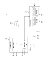
- amendment system 1 The figure which shows schematic structure of the liquid crystal display device 10.
- Flow chart showing processing of correction system 1 Flow chart showing initial correction processing
- Flow chart showing saving process 6 is a flowchart illustrating a reading process according to the first embodiment.
- the figure which shows the required time of this embodiment Diagram showing the time required for the prior art 7 is a flowchart illustrating reading processing according to the second embodiment.
- ⁇ Embodiment 1> The first embodiment will be described with reference to the drawings. In the following embodiments, description will be made using a liquid crystal display device including a liquid crystal panel as the display device.
- the display device to which the present invention can be applied is not limited to this, and can also be applied to an active matrix display device such as a PDP (plasma display panel) display device or an organic EL (electroluminescence) display device. is there.
- the system 1 includes a liquid crystal display device 10, a signal source 62, a computer 64, and a camera (an example of a photographing unit) 66.
- the liquid crystal display device 10 includes a supply circuit 12 and a liquid crystal panel (an example of a display panel) 40, and is connected to a signal source 62 via an input line 18.
- the supply circuit 12 supplies the image data G transmitted from the signal source 62 to the liquid crystal panel 40 via the supply line 20 and displays it on the display area 42 of the liquid crystal panel 40.
- the camera 66 is disposed in front of the liquid crystal panel 40 and photographs the display area 42 of the liquid crystal panel 40.
- the computer 64 is connected to the signal source 62, the camera 66, and the supply circuit 12 of the liquid crystal display device 10.
- Various programs P1 for controlling each component of the correction system 1 are stored in the computer 64.
- the computer 64 functions as a control unit 72 according to the program P1, and includes a signal source 62 and a camera 66. , Control the supply circuit 12 and the computer 64 itself.
- the photographing result W photographed by the camera 66 is transmitted to the computer 64, and the correction data H of the liquid crystal panel 40 is generated from the photographing result W.
- the computer 64 functions as a generation unit 70 that generates the correction data H from the imaging result W.
- the computer 64 inputs the generated correction data H to the supply circuit 12.
- the computer 64 transmits correction data H to the supply circuit 12 via the signal source 62, the input line 18 through which the image data G is transmitted to the supply circuit 12, and the correction data H to the supply circuit 12.
- the input lines 18 transmitted are equal.
- FIG. 2 shows the configuration of the liquid crystal display device 10.
- the liquid crystal display device 10 includes a supply circuit 12, a display unit 14, and a backlight drive circuit 16.
- the display unit 14 includes a liquid crystal panel 40 and a backlight unit 50.
- the backlight unit 50 is disposed on the back surface of the liquid crystal panel 40.
- the backlight unit 50 includes an LED 54 (Light Emitting Diode), which is a light source, and a light guide plate 52.
- the LED 54 is disposed to face the side surface of the light guide plate 52.
- the light guide plate 52 is disposed so that its main surface 52A faces the liquid crystal panel 40. In the light guide plate 52, the light incident on the side surface 52 ⁇ / b> B from the LED 54 is guided to the main surface 52 ⁇ / b> A facing the liquid crystal panel 40. Therefore, the side surface of the light guide plate 52 functions as a light incident surface 52 ⁇ / b> B that takes light emitted from the LEDs 54 into the light guide plate 52.
- the main surface of the light guide plate 52 functions as a light output surface 52 ⁇ / b> A that irradiates the liquid crystal panel 40 with light guided through the light guide plate 52.
- the backlight unit 50 is of a so-called edge light type (side light type) in which the LEDs 54 are arranged at both ends on the long side and the light guide plate 52 is arranged at the center thereof.
- the backlight drive circuit 16 is connected to the LEDs 54 constituting the backlight unit 50.
- the backlight drive circuit 16 supplies current to each LED 54, and controls the amount of light incident on the light guide plate 52 from each LED 54 by controlling the amount of current supplied.
- the supply circuit 12 includes an arithmetic circuit 22, a FLASH memory 24, and a DRAM (an example of a storage unit) 26.
- the FLASH memory 24 is a nonvolatile storage device and stores various programs P2 for controlling the operation of the arithmetic circuit 22.
- the arithmetic circuit 22 operates according to the program P2 read from the FLASH memory 24 or according to a command input from the computer 64.
- the DRAM 26 is a volatile storage device and stores correction data H transmitted from the computer 64.
- the arithmetic circuit 22 receives image data G from the signal source 62, functions as a supply unit 32, supplies the image data G to the liquid crystal panel 40, and displays the liquid crystal panel 40.
- the arithmetic circuit 22 reads the correction data H from the DRAM 26, corrects the image data G transmitted from the signal source 62 using the correction data H, The corrected image data G ′ is supplied to the liquid crystal panel 40.
- the arithmetic circuit 22 functions as the correction unit 34 that corrects the image data G using the correction data H read from the DRAM 26 and generates corrected image data G ′.
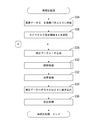
- the computer 64 starts the process when the liquid crystal panel 40 or the liquid crystal display device 10 including the liquid crystal panel 40 is set by the user to configure the correction system 1 and a correction instruction for the liquid crystal panel 40 is input from the user.
- the computer 64 first executes an initial correction process (S2).
- the computer 64 controls the signal source 62 and inputs the image data G to the supply circuit 12 (S12).
- the signal source 62 stores image data G for displaying a solid pattern of reference gradation values in advance, and when the signal source 62 receives a command from the computer 64, the image data G is supplied to the supply circuit 12.
- Send When the arithmetic circuit 22 receives the image data G from the signal source 62, the arithmetic circuit 22 functions as the supply unit 32, and supplies the image data G to the liquid crystal panel 40 in accordance with a command from the computer 64 (S14) to display the liquid crystal panel 40.
- the computer 64 controls the camera 66 to photograph the display area 42 when the liquid crystal panel 40 displays (S16), and transmits the photographing result W to the computer 64.
- correction data H1 means correction data generated by the computer 64.
- the photographing result W includes a photographing result corresponding to each pixel P of the liquid crystal panel 40, and the computer 64 detects the luminance variation B of the photographing result of each pixel P, and the luminance variation B is transmitted to the computer 64.
- Correction data H1 corresponding to each pixel P is generated so as to be within a pre-stored specified range KH.
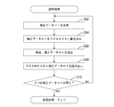
- the computer 64 executes a reading process for transmitting the correction data H1 from the computer 64 to the supply circuit 12 (S20). As shown in FIG. 8, in the reading process, the computer 64 transmits the correction data H1 to the supply circuit 12 (S62). When receiving the correction data H1, the arithmetic circuit 22 writes the correction data H1 into the DRAM 26 and stores it in the DRAM 26 (S64).
- the computer 64 transmits the same correction data H1 to the supply circuit 12 again when a predetermined time necessary for writing the correction data H1 has elapsed since the previous transmission of the correction data H1 (S66).
- the arithmetic circuit 22 reads the correction data H1 stored in the DRAM 26 (S68), and compares the correction data H1 received again with the correction data H1 read from the DRAM 26 (S70).
- the computer 64 ends the reading process.
- these two correction data H1 are different (S70: NO)
- the processing from S62 to S70 is repeated.
- the computer 64 executes a correction process (S22).
- the computer 64 controls the signal source 62 and inputs the image data G to the supply circuit 12.
- the arithmetic circuit 22 functions as the correction unit 34, reads the correction data H1 stored in the DRAM 26, corrects the image data G, and generates corrected image data G ′. .
- the arithmetic circuit 22 changes the correction data H ⁇ b> 1 stored in the DRAM 26 to the correction data H ⁇ b> 2 and ends the initial correction process.
- “correction data H2” means correction data stored in the DRAM 26 until the next correction processing after the correction processing, and means correction data used in the previous correction processing.
- the computer 64 After completing the initial correction process, the computer 64 functions as the control unit 72 and executes the re-correction process (S4). As shown in FIG. 5, in the recorrection process, the computer 64 controls the arithmetic circuit 22 to redisplay the liquid crystal panel 40. When receiving the command from the computer 64, the arithmetic circuit 22 functions as the supply unit 32, supplies the corrected image data G ′ generated in S22 to the liquid crystal panel 40 (S24), and redisplays the liquid crystal panel 40. The computer 64 images the display area 42 when the liquid crystal panel 40 displays (S26), and transmits the imaging result W ′ to the computer 64.
- the computer 64 generates new correction data H1 from the photographing result W ′ (S28), and transmits the correction data H1 to the supply circuit 12 (S30).
- These processes (S28, S30) in the re-correction process are the same processes as the processes of the same name (S18, S20) in the initial correction process, and redundant description is omitted.
- the arithmetic circuit 22 executes the addition process after the reading process (S30) for receiving the correction data H1 (S32).
- the arithmetic circuit 22 reads the correction data H1 and H2 stored in the DRAM 26 and adds them to generate the correction data H.
- the arithmetic circuit 22 writes the generated correction data H into the DRAM 26 and stores it in the DRAM 26 (S34).
- Correction data H correction data H1 + correction data H2
- correction data H is correction data generated again by adding correction data H1 newly generated this time to correction data H2 which is correction data used in the previous correction processing.
- correction can be made by adding the correction data H1 to the display unevenness that cannot be corrected by the correction data H2, and the correction accuracy is improved compared to the correction data H2. .
- the computer 64 executes a correction process (S36).
- the computer 64 controls the signal source 62 and inputs the image data G to the supply circuit 12.
- the arithmetic circuit 22 functions as the correction unit 34, reads the correction data H stored in the DRAM 26, corrects the image data G, and generates corrected image data G ′′.
- the re-correction process is finished.
- “corrected image data G ′′” is corrected image data generated using the corrected data H generated again, and can be said to be corrected image data generated again.
- the computer 64 executes determination processing after completing the re-correction processing (S6). As shown in FIG. 6, in the determination process, the computer 64 controls the arithmetic circuit 22 to redisplay the liquid crystal panel 40. When the arithmetic circuit 22 receives an instruction from the computer 64, the arithmetic circuit 22 functions as the supply unit 32, supplies the corrected image data G ′′ generated in S36 to the liquid crystal panel 40 (S42), and redisplays the liquid crystal panel 40. . The computer 64 images the display area 42 displayed on the liquid crystal panel 40 (S44), and transmits the imaging result W ′′ to the computer 64.
- the computer 64 Upon receiving the imaging result W ′′, the computer 64 detects the luminance variation B ′′ of the imaging result W ′′ and compares the detected luminance variation B ′′ with the specified range KH (S46). When the detected luminance variation B ′′ is within the specified range KH (S46: YES), the computer 64 ends the determination process. At this time, the computer 64 erases the correction data H and H1 stored in the DRAM 26. On the other hand, when the detected luminance variation B ′′ is larger than the specified range KH (S46: NO), the determination process is interrupted. The computer 64 returns to the re-correction process and executes the processes from S28 again.
- the computer 64 controls the arithmetic circuit 22 to erase the correction data H1 and H2 stored in the DRAM 26. Further, the computer 64 changes the correction data H stored in the DRAM 26 to the correction data H2.
- the computer 64 starts processing using the imaging result W ′′ captured in S44 as the imaging result W ′ captured in S26. That is, after returning to the recorrection process, the computer 64 executes the processes from S28 again without performing the processes of S24 and S26. That is, it is avoided that the display and photographing of the same corrected image data G ′′ are repeatedly performed in the determination step and the subsequent recorrection processing.
- the computer 64 executes a storage process (S8). As shown in FIG. 7, in the storage process, the computer 64 transmits the correction data H1 to the supply circuit 12 (S52), and executes an addition process (S54). These processes (S52, S54) of the storage process are the same processes as the processes of the same name (S30, S32) in the recorrection process, and a duplicate description is omitted.
- the computer 64 controls the arithmetic circuit 22 to execute a writing process for writing the correction data H into the FLASH memory 24 (S56).
- the arithmetic circuit 22 confirms whether or not the correction data H has been erased from the FLASH memory 24 in accordance with an instruction from the computer 64 (S82).
- the arithmetic circuit 22 keeps the correction data H already written in the FLASH memory 24 (S82: NO).
- the correction data H generated in S54 is written into the FLASH memory 24 and stored in the FLASH memory 24 (S86).
- the arithmetic circuit 22 When the arithmetic circuit 22 finishes writing the correction data H to the FLASH memory 24, the arithmetic circuit 22 reads the correction data H stored in the FLASH memory 24 (S88) and compares it with the correction data H stored in the DRAM 26 (S90). . When these two correction data H are equal (S90: YES), the computer 64 ends the writing process and ends the process. On the other hand, when these two correction data H are different (S90: NO), the processing from S82 to S90 is repeated.
- the corrected image data G ′ generated from the photographing result W is liquid crystal.
- the processes (S16 to S24, S26 to S42) until redisplayed on the panel 40 are repeatedly executed. While these processes are being executed, the correction data H (H1, H2) is a volatile storage device. Store in the DRAM 26. According to the correction system 1, the DRAM 26 is used as a storage device that stores the correction data H, so that the time required for processing can be shortened.
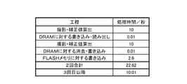
- FIG. 10 shows the time required for the processing of this embodiment.
- FIG. 11 shows the time required for correction processing when the conventional correction system is used, that is, when processing from acquisition of the imaging result W to redisplay of the liquid crystal panel 40 is executed using a nonvolatile storage device. Shown in comparison.
- the time required for these processes is shortened by replacing the time for writing and reading with respect to the DRAM 26 with the time for writing and reading with respect to the FLASH memory 24 of the prior art.
- the time required for these processes is shortened by replacing the time for erasing and writing with respect to the DRAM 26 with the time for erasing and writing with respect to the conventional FLASH memory 24. Therefore, in the correction process of the present embodiment, even when the process from the acquisition of the imaging result W to the redisplay of the liquid crystal panel 40 is repeatedly executed, the time required for the process can be reduced.
- the process of generating the correction data H is executed a plurality of times.
- noise may occur in the camera 66, or an imaging error due to a filter attached to the camera 66 may occur.
- a calculation error may occur, and a technique such as data compression is used to generate correction data as large as about 4 megabits in a short time. It is necessary to use this, and calculation errors may occur.
- even the correction data H generated through appropriate processing from the photographing result W may include an error, and the correction data H obtained by one generation processing accurately displays the display unevenness of the liquid crystal panel 40. It may not be possible to correct well.
- correction data H1 generated from the latest photographing result W and the DRAM 26 are stored in the previous correction processing.
- Correction data H is generated by adding the correction data H2 used, and correction processing is executed using the correction data H. Accordingly, it is possible to generate correction data H with higher accuracy by combining the correction data H generated a plurality of times, and display unevenness of the liquid crystal panel 40 can be corrected with high accuracy.
- the same correction data H1 is transmitted from the computer 64 to the supply circuit 12 twice, and the calculation circuit 22 to which the correction data H is input A so-called Verify operation is performed to check whether or not these correction data H1 match. That is, the Verify operation is executed in the device to which predetermined data is input. Accordingly, when a communication error occurs in transmission of the correction data H from the computer 64 to the supply circuit 12, generation of the corrected image data G ′ using the correction data H in which the communication error has occurred is suppressed, and the display is performed. The display unevenness of the panel can be corrected with high accuracy.
- the input line 18 to which the image data G is input to the supply circuit 12 and the input line 18 to which the correction data H is input to the supply circuit 12 are equal. Even when the image data G is sent using the input line 18 to which data whose transmission direction is determined in advance is transmitted, a communication error can be detected and display unevenness of the liquid crystal panel 40 can be corrected with high accuracy. Can do.
- the correction system 1 of the present embodiment has identification image data (identification symbol of the identification symbol) that informs the FLASH memory 24 of the supply circuit 12 of the occurrence of a communication error between the computer 64 and the supply circuit 12.
- identification image data identification symbol of the identification symbol
- K is stored. In the following description, the same description as that of the first embodiment will not be repeated.
- the arithmetic circuit 22 compares these two correction data H1 (S70).
- the correction data H1 is the identification image data K stored in the FLASH memory 24 as shown in FIG.
- Identification image data K for displaying “ ⁇ ”, which is an identification image indicating equality, is read and output to the liquid crystal panel 40 via the supply line 20 (S72). As a result, “ ⁇ ” is displayed on the liquid crystal panel 40.
- the arithmetic circuit 22 indicates that the correction data H1 is different among the identification image data K stored in the FLASH memory 24 as shown in FIG.
- the identification image data K for displaying “x”, which is an identification image indicating “”, is read and output to the liquid crystal panel 40 via the supply line 20 (S74). As a result, “x” is displayed on the liquid crystal panel 40.
- the computer 64 images the display area 42 when the identification image is displayed on the liquid crystal panel 40, and transmits the imaging result W ′ to the computer 64.
- the computer 64 confirms the photographing result W ′ and detects that “ ⁇ ” is included in the photographing result W ′, the reading process ends.
- the processing from S ⁇ b> 62 is repeated and the correction data H ⁇ b> 1 is supplied to the supply circuit 12 again.
- the computer 64 can detect the identification image using the camera 66, and between the computer 64 and the supply circuit 12. It is possible to detect that a communication error has occurred. When a communication error occurs, the computer 64 further supplies correction data H1 to the supply circuit 12, thereby generating corrected image data G ′ based on the correction data H1 input when the communication error occurs. It can be suppressed.
- a third embodiment will be described with reference to FIG.
- a plurality of conversion patterns C for converting correction data H1 input from the computer 64 to the supply circuit 12 are stored in the computer 64 as indicated by dotted lines in FIG. This is different from the correction system 1 of the first embodiment. In the following description, the same description as that of the first embodiment will not be repeated.
- the computer 64 converts the correction data H1 with the first conversion pattern C1 prior to inputting the correction data H1 to the supply circuit 12 at S62 (S61).
- the converted correction data H1 is input to the supply circuit 12.
- the correction data H1 Prior to inputting the correction data H1 to the supply circuit 12 in S66, the correction data H1 is converted with a second conversion pattern C2 different from the first conversion pattern C1 (S65), and the converted correction data H1 is supplied to the supply circuit. 12 is input.
- the arithmetic circuit 22 compares these two correction data H1 (S70).
- the arithmetic circuit 22 converts the correction data H1 received in S62 again based on the first conversion pattern C1. Further, the correction data H1 received in S66 is converted again based on the second conversion pattern C2. The arithmetic circuit 22 compares the two converted correction data H1 and checks whether they are equal.
- the computer 64 stores a plurality of conversion patterns C, and the correction data H1 input to the supply circuit 12 is converted using the conversion patterns C, whereby the computer 64 and the detection accuracy of a communication error occurring between the supply circuit 12 is improved.
- a communication error that occurs between the computer 64 and the supply circuit 12 includes a disconnection of the input line 18.
- correction data H ⁇ b> 1 in which all signals indicate “0” or “1” is input to the supply circuit 12.
- the arithmetic circuit 22 that has received the correction data H1 mistakenly indicates that no communication error has occurred because the correction data H1 received at different timings is the same although the input correction data H1 is incorrect. It will be detected.
- the computer 64 converts the correction data H1 using the first conversion pattern C1 and the second conversion pattern C2 that are different from each other. To do.
- the arithmetic circuit 22 reconverts the received correction data H1 using these conversion patterns C and checks whether they are equal. Therefore, even when the correction data H1 is equal when the arithmetic circuit 22 receives the correction data H1, if the reconverted correction data H1 is not equal, a communication error can be detected, and a communication error can be detected. Accuracy can be improved.
- the correction data H is generated based on the luminance variation B of the imaging result W, and the example of determining whether to end the determination process has been described. Is not limited to this.
- the processing may be performed based on the chromaticity variation together with the luminance variation B of the photographing result W.
- the DRAM 26 may be provided inside the arithmetic circuit 22.
- the process in which the arithmetic circuit 22 writes the correction data H to the DRAM 26 is an internal process of the arithmetic circuit 22, and the time required for the process performed in the correction system 1 may be further shortened.
- the embodiment of the invention is not limited to this.
- a test result may be output using a connection line connected to a serial communication bus such as I2C.
- the data output as the inspection result is not limited to the identification image data K, and is appropriately changed to a necessary form.
- the identification image data K is output to the liquid crystal panel 40 via the supply line 20, the identification image is not limited to “ ⁇ ” or “ ⁇ ”. Furthermore, it is not necessary to be “image data”. For example, any process that can be recognized by the camera 66, such as reducing the brightness of the backlight unit 50, may be used.
- the light source using the LED as the light source is exemplified, but a light source other than the LED may be used.
- correction system 10: liquid crystal display device, 12: supply circuit, 14: display unit, 18: input line, 20: supply line, 22: arithmetic circuit, 24: FLASH memory, 26: DRAM, 32: supply unit, 34: correction unit, 40: liquid crystal panel, 42: display area, 62: signal source, 64: computer, 66: camera, 70: generation unit, 72: control unit, B: luminance variation, G: image data, G ′ , G ′′: correction image data, H, H1, H2: correction data, KH: specified range, W: photographing result, C: conversion pattern, K: identification image data
Landscapes
- Engineering & Computer Science (AREA)
- Physics & Mathematics (AREA)
- Computer Hardware Design (AREA)
- General Physics & Mathematics (AREA)
- Theoretical Computer Science (AREA)
- Control Of Indicators Other Than Cathode Ray Tubes (AREA)
- Liquid Crystal Display Device Control (AREA)
Abstract
La présente invention concerne un procédé pour la correction de manque d'uniformité d'un écran à cristaux liquides (40) comprenant les étapes suivantes: 1) la fourniture de données d'images à l'écran de cristaux liquides (40) et l'affichage des données d'images sur l'écran à cristaux liquides (40); 2) la prise de vue d'une région de l'écran à cristaux liquides (40) avec une caméra (66) ; 3) la génération de données de correction de l'écran à cristaux liquides (40) à partir d'un résultat de la photographie ; 4) le stockage des données de correction sur un dispositif de stockage non volatile ; 5) la génération de données d'images corrigées au moyen des données de correction qui sont stockées dans le dispositif de stockage non volatile ; 6) la fourniture des données d'images corrigées à l'écran à cristaux liquides (40) et un nouvel affichage des données d'images corrigées sur l'écran à cristaux liquides (40) ; et 7) la répétition des étapes 2 à 6.
Priority Applications (1)
| Application Number | Priority Date | Filing Date | Title |
|---|---|---|---|
| US14/001,733 US9183811B2 (en) | 2011-04-01 | 2012-04-02 | Method of correcting unevenness of display panel and correction system |
Applications Claiming Priority (2)
| Application Number | Priority Date | Filing Date | Title |
|---|---|---|---|
| JP2011-081944 | 2011-04-01 | ||
| JP2011081944 | 2011-04-01 |
Publications (1)
| Publication Number | Publication Date |
|---|---|
| WO2012133890A1 true WO2012133890A1 (fr) | 2012-10-04 |
Family
ID=46931577
Family Applications (1)
| Application Number | Title | Priority Date | Filing Date |
|---|---|---|---|
| PCT/JP2012/058908 Ceased WO2012133890A1 (fr) | 2011-04-01 | 2012-04-02 | Procédé de correction de manque d'uniformité d'écran d'affichage, système de correction |
Country Status (2)
| Country | Link |
|---|---|
| US (1) | US9183811B2 (fr) |
| WO (1) | WO2012133890A1 (fr) |
Cited By (6)
| Publication number | Priority date | Publication date | Assignee | Title |
|---|---|---|---|---|
| CN103943092A (zh) * | 2014-05-05 | 2014-07-23 | 广东威创视讯科技股份有限公司 | 一种显示单元内屏幕颜色校正方法及系统 |
| CN104166250A (zh) * | 2013-05-20 | 2014-11-26 | 冠捷投资有限公司 | 一种平面显示器面板均匀度检测方法及其系统 |
| JP2020086419A (ja) * | 2018-11-28 | 2020-06-04 | 雄二 橋本 | 複数の制御対象のユニフォーミティを得るための調整方法、調整システムおよびコンベア装置、並びに調整された機器。 |
| JP2020086409A (ja) * | 2018-11-30 | 2020-06-04 | 株式会社イクス | ムラ補正データ生成方法及びムラ補正データ生成システム |
| US10909895B2 (en) | 2016-12-20 | 2021-02-02 | Sakai Display Products Corporation | Correction system, display panel, display device, correction method, and storage medium |
| US11017701B2 (en) | 2018-09-14 | 2021-05-25 | Sakai Display Products Corporation | Correction data generating device, computer program, method for generating correction data, and method for producing display panel |
Families Citing this family (10)
| Publication number | Priority date | Publication date | Assignee | Title |
|---|---|---|---|---|
| US20100214282A1 (en) | 2009-02-24 | 2010-08-26 | Dolby Laboratories Licensing Corporation | Apparatus for providing light source modulation in dual modulator displays |
| US9564078B2 (en) | 2010-12-17 | 2017-02-07 | Dolby Laboratories Licensing Corporation | Quantum dots for display panels |
| KR102118309B1 (ko) | 2012-09-19 | 2020-06-03 | 돌비 레버러토리즈 라이쎈싱 코오포레이션 | 양자점/리모트 인광 디스플레이 시스템 개선 |
| KR102115146B1 (ko) | 2013-03-08 | 2020-05-26 | 돌비 레버러토리즈 라이쎈싱 코오포레이션 | 광 변환을 갖는 이중 변조 디스플레이 기술들 |
| JP6358441B2 (ja) * | 2013-12-20 | 2018-07-18 | パナソニックIpマネジメント株式会社 | 表示むら補正装置、表示装置、表示むら補正方法および表示装置の製造方法 |
| US10262603B2 (en) | 2014-03-26 | 2019-04-16 | Dolby Laboratories Licensing Corporation | Global light compensation in a variety of displays |
| CN105607317B (zh) * | 2016-03-24 | 2018-11-23 | 京东方科技集团股份有限公司 | 显示器亮度调整方法、测试方法及装置、显示器测试设备 |
| KR102535803B1 (ko) * | 2018-08-13 | 2023-05-24 | 삼성디스플레이 주식회사 | 얼룩 보정을 수행하는 표시 장치 및 표시 장치의 구동 방법 |
| US11290628B2 (en) | 2018-12-27 | 2022-03-29 | Dynascan Technology Corp. | Display apparatus |
| US11200656B2 (en) * | 2019-01-11 | 2021-12-14 | Universal City Studios Llc | Drop detection systems and methods |
Citations (8)
| Publication number | Priority date | Publication date | Assignee | Title |
|---|---|---|---|---|
| JPS61243495A (ja) * | 1985-04-20 | 1986-10-29 | 三洋電機株式会社 | 液晶表示装置の表示むら補償方法 |
| JPH0431120U (fr) * | 1990-07-10 | 1992-03-12 | ||
| JPH07261719A (ja) * | 1994-03-24 | 1995-10-13 | Semiconductor Energy Lab Co Ltd | 表示装置の補正システムおよびその動作方法 |
| JP2001290710A (ja) * | 2000-04-10 | 2001-10-19 | Toshiba Corp | データエラー検出装置 |
| JP2003177714A (ja) * | 2001-09-28 | 2003-06-27 | Semiconductor Energy Lab Co Ltd | 発光装置及び電子機器 |
| JP2006017891A (ja) * | 2004-06-30 | 2006-01-19 | Canon Inc | 表示装置およびテレビジョン装置 |
| JP2009168883A (ja) * | 2008-01-11 | 2009-07-30 | Seiko Epson Corp | 画像表示装置 |
| JP2010066352A (ja) * | 2008-09-09 | 2010-03-25 | Seiko Epson Corp | 測定装置、補正データ生成装置、測定方法、補正データ生成方法、および補正データ生成プログラム |
Family Cites Families (6)
| Publication number | Priority date | Publication date | Assignee | Title |
|---|---|---|---|---|
| JP2001075542A (ja) | 2000-07-10 | 2001-03-23 | Semiconductor Energy Lab Co Ltd | 補正システムおよびその動作方法 |
| SG120888A1 (en) | 2001-09-28 | 2006-04-26 | Semiconductor Energy Lab | A light emitting device and electronic apparatus using the same |
| JP5010814B2 (ja) * | 2005-07-07 | 2012-08-29 | グローバル・オーエルイーディー・テクノロジー・リミテッド・ライアビリティ・カンパニー | 有機el表示装置の製造方法 |
| US8406562B2 (en) * | 2006-08-11 | 2013-03-26 | Geo Semiconductor Inc. | System and method for automated calibration and correction of display geometry and color |
| CN101377918B (zh) * | 2008-09-19 | 2013-02-27 | 李鑫 | 一种电子显示屏系统、电子显示屏亮度校正方法及系统 |
| KR101200499B1 (ko) * | 2010-08-20 | 2012-11-12 | 전자부품연구원 | 표시장치 및 백라이트 제어방법 |
-
2012
- 2012-04-02 WO PCT/JP2012/058908 patent/WO2012133890A1/fr not_active Ceased
- 2012-04-02 US US14/001,733 patent/US9183811B2/en not_active Expired - Fee Related
Patent Citations (8)
| Publication number | Priority date | Publication date | Assignee | Title |
|---|---|---|---|---|
| JPS61243495A (ja) * | 1985-04-20 | 1986-10-29 | 三洋電機株式会社 | 液晶表示装置の表示むら補償方法 |
| JPH0431120U (fr) * | 1990-07-10 | 1992-03-12 | ||
| JPH07261719A (ja) * | 1994-03-24 | 1995-10-13 | Semiconductor Energy Lab Co Ltd | 表示装置の補正システムおよびその動作方法 |
| JP2001290710A (ja) * | 2000-04-10 | 2001-10-19 | Toshiba Corp | データエラー検出装置 |
| JP2003177714A (ja) * | 2001-09-28 | 2003-06-27 | Semiconductor Energy Lab Co Ltd | 発光装置及び電子機器 |
| JP2006017891A (ja) * | 2004-06-30 | 2006-01-19 | Canon Inc | 表示装置およびテレビジョン装置 |
| JP2009168883A (ja) * | 2008-01-11 | 2009-07-30 | Seiko Epson Corp | 画像表示装置 |
| JP2010066352A (ja) * | 2008-09-09 | 2010-03-25 | Seiko Epson Corp | 測定装置、補正データ生成装置、測定方法、補正データ生成方法、および補正データ生成プログラム |
Cited By (8)
| Publication number | Priority date | Publication date | Assignee | Title |
|---|---|---|---|---|
| CN104166250A (zh) * | 2013-05-20 | 2014-11-26 | 冠捷投资有限公司 | 一种平面显示器面板均匀度检测方法及其系统 |
| CN103943092A (zh) * | 2014-05-05 | 2014-07-23 | 广东威创视讯科技股份有限公司 | 一种显示单元内屏幕颜色校正方法及系统 |
| US10909895B2 (en) | 2016-12-20 | 2021-02-02 | Sakai Display Products Corporation | Correction system, display panel, display device, correction method, and storage medium |
| US11017701B2 (en) | 2018-09-14 | 2021-05-25 | Sakai Display Products Corporation | Correction data generating device, computer program, method for generating correction data, and method for producing display panel |
| JP2020086419A (ja) * | 2018-11-28 | 2020-06-04 | 雄二 橋本 | 複数の制御対象のユニフォーミティを得るための調整方法、調整システムおよびコンベア装置、並びに調整された機器。 |
| JP2023051934A (ja) * | 2018-11-28 | 2023-04-11 | 雄二 橋本 | 複数の制御対象のユニフォーミティを得るための調整方法、調整システムおよびコンベア装置、並びに調整された機器。 |
| JP7503731B2 (ja) | 2018-11-28 | 2024-06-21 | 雄二 橋本 | コンベア装置 |
| JP2020086409A (ja) * | 2018-11-30 | 2020-06-04 | 株式会社イクス | ムラ補正データ生成方法及びムラ補正データ生成システム |
Also Published As
| Publication number | Publication date |
|---|---|
| US20130342558A1 (en) | 2013-12-26 |
| US9183811B2 (en) | 2015-11-10 |
Similar Documents
| Publication | Publication Date | Title |
|---|---|---|
| WO2012133890A1 (fr) | Procédé de correction de manque d'uniformité d'écran d'affichage, système de correction | |
| CN110648614B (zh) | 用于测试显示面板的装置及其驱动方法 | |
| CN110301000B (zh) | 用于显示装置的亮度不均补偿的方法及相应的显示装置 | |
| KR102672867B1 (ko) | 디스플레이 구동기를 설정하는 디바이스 및 방법 | |
| KR102307501B1 (ko) | 광학 보상 시스템 및 광학 보상 방법 | |
| CN108877631A (zh) | 显示屏的Mura补偿方法、装置、计算机设备及存储介质 | |
| US11335221B2 (en) | Method, device and system for detecting display panel | |
| US9274328B2 (en) | Image processing apparatus, microscope system, and recording medium | |
| US11994961B2 (en) | Image display system, image processor circuit, and panel driving method | |
| US11334308B2 (en) | Display device and image correction method | |
| KR102746914B1 (ko) | 전자 장치, 디스플레이 장치 및 그 제어 방법 | |
| WO2017024652A1 (fr) | Procédé permettant de démarrer un dispositif d'affichage à cristaux liquides | |
| WO2011118275A1 (fr) | Procédé de commande de panneau d'affichage, circuit de commande de panneau d'affichage, dispositif d'affichage | |
| JP5679356B2 (ja) | 補正方法及び表示装置 | |
| US20150035848A1 (en) | Display apparatus and control method thereof | |
| CN116386564A (zh) | 校正输入图像数据的方法和执行该方法的发光显示设备 | |
| WO2013115356A1 (fr) | Dispositif d'affichage d'image, appareil électronique, caméra électronique, et terminal d'informations | |
| KR102741076B1 (ko) | 곡면형 평판 표시장치와 그 구동방법 | |
| CN113963671B (zh) | 一种显示方法、终端及存储介质 | |
| US20210043121A1 (en) | Display apparatus | |
| KR20220027358A (ko) | 광학 보상 장치 및 이를 포함하는 광학 보상 시스템 | |
| KR20200105459A (ko) | 표시장치의 얼룩 보상 방법 및 및 장치 | |
| JP5347488B2 (ja) | 投影装置 | |
| CN211505255U (zh) | 显示面板检测装置及系统 | |
| CN113272886A (zh) | 校正图像生成系统、图像控制方法、图像控制程序以及记录介质 |
Legal Events
| Date | Code | Title | Description |
|---|---|---|---|
| 121 | Ep: the epo has been informed by wipo that ep was designated in this application |
Ref document number: 12763709 Country of ref document: EP Kind code of ref document: A1 |
|
| WWE | Wipo information: entry into national phase |
Ref document number: 14001733 Country of ref document: US |
|
| NENP | Non-entry into the national phase |
Ref country code: DE |
|
| 122 | Ep: pct application non-entry in european phase |
Ref document number: 12763709 Country of ref document: EP Kind code of ref document: A1 |
|
| NENP | Non-entry into the national phase |
Ref country code: JP |