WO2012133894A1 - 照明装置、表示装置、及びテレビ受信装置 - Google Patents
照明装置、表示装置、及びテレビ受信装置 Download PDFInfo
- Publication number
- WO2012133894A1 WO2012133894A1 PCT/JP2012/058934 JP2012058934W WO2012133894A1 WO 2012133894 A1 WO2012133894 A1 WO 2012133894A1 JP 2012058934 W JP2012058934 W JP 2012058934W WO 2012133894 A1 WO2012133894 A1 WO 2012133894A1
- Authority
- WO
- WIPO (PCT)
- Prior art keywords
- light
- connector
- light source
- led
- bottom plate
- Prior art date
- Legal status (The legal status is an assumption and is not a legal conclusion. Google has not performed a legal analysis and makes no representation as to the accuracy of the status listed.)
- Ceased
Links
Images








Classifications
-
- H—ELECTRICITY
- H04—ELECTRIC COMMUNICATION TECHNIQUE
- H04N—PICTORIAL COMMUNICATION, e.g. TELEVISION
- H04N5/00—Details of television systems
- H04N5/64—Constructional details of receivers, e.g. cabinets or dust covers
- H04N5/655—Construction or mounting of chassis, e.g. for varying the elevation of the tube
-
- H—ELECTRICITY
- H04—ELECTRIC COMMUNICATION TECHNIQUE
- H04N—PICTORIAL COMMUNICATION, e.g. TELEVISION
- H04N5/00—Details of television systems
- H04N5/66—Transforming electric information into light information
-
- G—PHYSICS
- G02—OPTICS
- G02F—OPTICAL DEVICES OR ARRANGEMENTS FOR THE CONTROL OF LIGHT BY MODIFICATION OF THE OPTICAL PROPERTIES OF THE MEDIA OF THE ELEMENTS INVOLVED THEREIN; NON-LINEAR OPTICS; FREQUENCY-CHANGING OF LIGHT; OPTICAL LOGIC ELEMENTS; OPTICAL ANALOGUE/DIGITAL CONVERTERS
- G02F1/00—Devices or arrangements for the control of the intensity, colour, phase, polarisation or direction of light arriving from an independent light source, e.g. switching, gating or modulating; Non-linear optics
- G02F1/01—Devices or arrangements for the control of the intensity, colour, phase, polarisation or direction of light arriving from an independent light source, e.g. switching, gating or modulating; Non-linear optics for the control of the intensity, phase, polarisation or colour
- G02F1/13—Devices or arrangements for the control of the intensity, colour, phase, polarisation or direction of light arriving from an independent light source, e.g. switching, gating or modulating; Non-linear optics for the control of the intensity, phase, polarisation or colour based on liquid crystals, e.g. single liquid crystal display cells
- G02F1/133—Constructional arrangements; Operation of liquid crystal cells; Circuit arrangements
- G02F1/1333—Constructional arrangements; Manufacturing methods
- G02F1/1335—Structural association of cells with optical devices, e.g. polarisers or reflectors
- G02F1/1336—Illuminating devices
- G02F1/133602—Direct backlight
- G02F1/133603—Direct backlight with LEDs
-
- G—PHYSICS
- G02—OPTICS
- G02F—OPTICAL DEVICES OR ARRANGEMENTS FOR THE CONTROL OF LIGHT BY MODIFICATION OF THE OPTICAL PROPERTIES OF THE MEDIA OF THE ELEMENTS INVOLVED THEREIN; NON-LINEAR OPTICS; FREQUENCY-CHANGING OF LIGHT; OPTICAL LOGIC ELEMENTS; OPTICAL ANALOGUE/DIGITAL CONVERTERS
- G02F1/00—Devices or arrangements for the control of the intensity, colour, phase, polarisation or direction of light arriving from an independent light source, e.g. switching, gating or modulating; Non-linear optics
- G02F1/01—Devices or arrangements for the control of the intensity, colour, phase, polarisation or direction of light arriving from an independent light source, e.g. switching, gating or modulating; Non-linear optics for the control of the intensity, phase, polarisation or colour
- G02F1/13—Devices or arrangements for the control of the intensity, colour, phase, polarisation or direction of light arriving from an independent light source, e.g. switching, gating or modulating; Non-linear optics for the control of the intensity, phase, polarisation or colour based on liquid crystals, e.g. single liquid crystal display cells
- G02F1/133—Constructional arrangements; Operation of liquid crystal cells; Circuit arrangements
- G02F1/1333—Constructional arrangements; Manufacturing methods
- G02F1/1335—Structural association of cells with optical devices, e.g. polarisers or reflectors
- G02F1/1336—Illuminating devices
- G02F1/133602—Direct backlight
- G02F1/133606—Direct backlight including a specially adapted diffusing, scattering or light controlling members
- G02F1/133607—Direct backlight including a specially adapted diffusing, scattering or light controlling members the light controlling member including light directing or refracting elements, e.g. prisms or lenses
-
- G—PHYSICS
- G02—OPTICS
- G02F—OPTICAL DEVICES OR ARRANGEMENTS FOR THE CONTROL OF LIGHT BY MODIFICATION OF THE OPTICAL PROPERTIES OF THE MEDIA OF THE ELEMENTS INVOLVED THEREIN; NON-LINEAR OPTICS; FREQUENCY-CHANGING OF LIGHT; OPTICAL LOGIC ELEMENTS; OPTICAL ANALOGUE/DIGITAL CONVERTERS
- G02F1/00—Devices or arrangements for the control of the intensity, colour, phase, polarisation or direction of light arriving from an independent light source, e.g. switching, gating or modulating; Non-linear optics
- G02F1/01—Devices or arrangements for the control of the intensity, colour, phase, polarisation or direction of light arriving from an independent light source, e.g. switching, gating or modulating; Non-linear optics for the control of the intensity, phase, polarisation or colour
- G02F1/13—Devices or arrangements for the control of the intensity, colour, phase, polarisation or direction of light arriving from an independent light source, e.g. switching, gating or modulating; Non-linear optics for the control of the intensity, phase, polarisation or colour based on liquid crystals, e.g. single liquid crystal display cells
- G02F1/133—Constructional arrangements; Operation of liquid crystal cells; Circuit arrangements
- G02F1/1333—Constructional arrangements; Manufacturing methods
- G02F1/1335—Structural association of cells with optical devices, e.g. polarisers or reflectors
- G02F1/1336—Illuminating devices
- G02F1/133602—Direct backlight
- G02F1/133608—Direct backlight including particular frames or supporting means
-
- G—PHYSICS
- G02—OPTICS
- G02F—OPTICAL DEVICES OR ARRANGEMENTS FOR THE CONTROL OF LIGHT BY MODIFICATION OF THE OPTICAL PROPERTIES OF THE MEDIA OF THE ELEMENTS INVOLVED THEREIN; NON-LINEAR OPTICS; FREQUENCY-CHANGING OF LIGHT; OPTICAL LOGIC ELEMENTS; OPTICAL ANALOGUE/DIGITAL CONVERTERS
- G02F1/00—Devices or arrangements for the control of the intensity, colour, phase, polarisation or direction of light arriving from an independent light source, e.g. switching, gating or modulating; Non-linear optics
- G02F1/01—Devices or arrangements for the control of the intensity, colour, phase, polarisation or direction of light arriving from an independent light source, e.g. switching, gating or modulating; Non-linear optics for the control of the intensity, phase, polarisation or colour
- G02F1/13—Devices or arrangements for the control of the intensity, colour, phase, polarisation or direction of light arriving from an independent light source, e.g. switching, gating or modulating; Non-linear optics for the control of the intensity, phase, polarisation or colour based on liquid crystals, e.g. single liquid crystal display cells
- G02F1/133—Constructional arrangements; Operation of liquid crystal cells; Circuit arrangements
- G02F1/1333—Constructional arrangements; Manufacturing methods
- G02F1/1335—Structural association of cells with optical devices, e.g. polarisers or reflectors
- G02F1/1336—Illuminating devices
- G02F1/133602—Direct backlight
- G02F1/133612—Electrical details
-
- G—PHYSICS
- G02—OPTICS
- G02F—OPTICAL DEVICES OR ARRANGEMENTS FOR THE CONTROL OF LIGHT BY MODIFICATION OF THE OPTICAL PROPERTIES OF THE MEDIA OF THE ELEMENTS INVOLVED THEREIN; NON-LINEAR OPTICS; FREQUENCY-CHANGING OF LIGHT; OPTICAL LOGIC ELEMENTS; OPTICAL ANALOGUE/DIGITAL CONVERTERS
- G02F1/00—Devices or arrangements for the control of the intensity, colour, phase, polarisation or direction of light arriving from an independent light source, e.g. switching, gating or modulating; Non-linear optics
- G02F1/01—Devices or arrangements for the control of the intensity, colour, phase, polarisation or direction of light arriving from an independent light source, e.g. switching, gating or modulating; Non-linear optics for the control of the intensity, phase, polarisation or colour
- G02F1/13—Devices or arrangements for the control of the intensity, colour, phase, polarisation or direction of light arriving from an independent light source, e.g. switching, gating or modulating; Non-linear optics for the control of the intensity, phase, polarisation or colour based on liquid crystals, e.g. single liquid crystal display cells
- G02F1/133—Constructional arrangements; Operation of liquid crystal cells; Circuit arrangements
- G02F1/136—Liquid crystal cells structurally associated with a semi-conducting layer or substrate, e.g. cells forming part of an integrated circuit
- G02F1/1362—Active matrix addressed cells
- G02F1/13624—Active matrix addressed cells having more than one switching element per pixel
-
- G—PHYSICS
- G02—OPTICS
- G02F—OPTICAL DEVICES OR ARRANGEMENTS FOR THE CONTROL OF LIGHT BY MODIFICATION OF THE OPTICAL PROPERTIES OF THE MEDIA OF THE ELEMENTS INVOLVED THEREIN; NON-LINEAR OPTICS; FREQUENCY-CHANGING OF LIGHT; OPTICAL LOGIC ELEMENTS; OPTICAL ANALOGUE/DIGITAL CONVERTERS
- G02F2201/00—Constructional arrangements not provided for in groups G02F1/00 - G02F7/00
- G02F2201/46—Fixing elements
- G02F2201/465—Snap -fit
-
- G—PHYSICS
- G02—OPTICS
- G02F—OPTICAL DEVICES OR ARRANGEMENTS FOR THE CONTROL OF LIGHT BY MODIFICATION OF THE OPTICAL PROPERTIES OF THE MEDIA OF THE ELEMENTS INVOLVED THEREIN; NON-LINEAR OPTICS; FREQUENCY-CHANGING OF LIGHT; OPTICAL LOGIC ELEMENTS; OPTICAL ANALOGUE/DIGITAL CONVERTERS
- G02F2201/00—Constructional arrangements not provided for in groups G02F1/00 - G02F7/00
- G02F2201/52—RGB geometrical arrangements
Definitions
- the present invention relates to a lighting device, a display device, and a television receiver.
- liquid crystal display device requires a backlight device as a separate illumination device because the liquid crystal panel used for this does not emit light.
- a direct-type backlight device that directly supplies light from the back surface to a liquid crystal panel.
- a direct type backlight device a light source substrate on which light sources such as LEDs are arranged is arranged along a bottom plate of a chassis as a casing.
- a wiring pattern for electrically connecting each light source is formed on the light source board, and a connector provided at one end of the power supply wiring extending from the power supply board is electrically connected to the terminal part provided at both ends of the wiring pattern. Connected. Thereby, electric power is supplied to each light source from a power supply board via a connector.
- Patent Document 1 A conventional example of such a direct type backlight device is disclosed in Patent Document 1, for example.
- one end surface of the light source substrate is arranged in parallel with one side plate of the chassis, and the wiring pattern on the end portion of the light source substrate having this one end surface is arranged.
- a connector is connected.
- a connector is connected with a wiring pattern by making the direction (direction which makes a right angle) going perpendicularly with respect to the said one end surface from said one side plate into a connection direction.
- the connector and the power supply wiring are arranged between the one side plate and the one end surface.
- the Rukoto For this reason, in the chassis, in order to accommodate the connector connected to the wiring pattern and the power supply wiring extending from the connector, it is necessary to provide a certain distance between the one side plate and the one end surface. However, when the distance between one side plate of the chassis and one end face of the light source substrate is increased, the width of the non-display area is increased, and the backlight device cannot be narrowed.
- An object of the present invention is to provide a technique capable of narrowing a frame in a direct-type illumination device in which power supply wiring is connected to an end portion side of a light source substrate.
- the present invention includes a bottom plate, a side plate rising from at least one end of the bottom plate to one surface side of the bottom plate, a housing member having a light output portion on the one surface side, and one end surface of the side plate
- a light source substrate disposed on the bottom plate of the housing member so as to face the side plate, a light source disposed on the light source substrate with the light output side of the housing member as a light emitting side, and a light source substrate disposed on the light source substrate.
- One electric power is supplied to the light source through the connection member and the pattern wiring.
- the second connection member connected to the first connection member overlaps the first connection member in plan view, so that the second connection member is disposed between the side plate of the housing member and one end surface of the light source substrate. It is possible to prevent the two connecting members from being arranged. For this reason, even if the side plate of the housing member is brought closer to one end surface side (the inside of the housing member) of the light source substrate, the second connecting member does not get in the way, and is orthogonal to the side plate side edge facing the one end surface of the light source substrate. Thus, the distance between the side plate of the housing member and the one end surface of the light source substrate can be relatively narrowed compared to the case where the direction from the end side toward the one end surface is the connection direction.
- the connecting member is not limited to the connector.
- a card-type connector that can be connected to the terminal portion may be a terminal portion provided with an electrode terminal from which one connection member is exposed.
- the second connecting member may be connected to the first connecting member from a direction overlapping the first connecting member in plan view. According to this configuration, when the second connection member is connected to the first connection member, the second connection member can be positioned in advance so as to overlap the first connection member in plan view. The second connecting member can be easily connected to the member.
- the second connection member may be connected to the first connection member from the opposite side across the first connection member from the side of the side plate facing the one end surface in plan view. According to this configuration, when the second connection member is connected to the first connection member, the side plate facing the one end surface can be prevented from becoming an obstacle. Can be easily connected.
- the bottom plate has a horizontally long rectangular shape, and the end sides thereof include a pair of first end sides along the short side direction of the bottom plate and a pair of second end sides along the long side direction of the bottom plate.
- the plurality of light source substrates are arranged on the bottom plate, and each of the one end faces the side plate rising from the first end side, and the plurality of light source substrates on the plurality of light source substrates.
- Each of the first connecting members may be arranged, and each of the plurality of first connecting members may be connected to the second connecting member.
- the distance between the side plate rising from the first end and the one end surface of the light source substrate can be reduced, and the lighting device can be narrowed. Can be achieved.
- Each of the plurality of light source substrates has a horizontally long rectangular shape such that both end surfaces on the short side are along the first end side, and both end surfaces on the long side are along the second end side.
- one of the short side end faces may be the one end face. According to this configuration, it is possible to achieve a narrow frame of the lighting device while realizing a lighting device having a configuration in which a plurality of light source substrates are arranged in a matrix in the housing member.
- Each of the plurality of light source boards is arranged such that each of the first connection members arranged on the light source board is arranged in a straight line along the first end side in a plan view, and the second connection The member has a linear shape along a direction parallel to the first end side, and one second connecting member is simultaneously connected to each of the plurality of first connecting members arranged in a straight line in a plan view. May be.
- the connection work between the first connection member and the second connection member can be simplified.
- the proportion of the power supply wires in the housing member can be reduced, and the lighting device can be further narrowed in frame.
- the wiring board may further include a wiring insertion hole that penetrates the bottom plate and through which the power supply wiring is inserted, and the wiring insertion hole may be provided on the center side of the bottom plate.
- each power supply wiring extended from each 2nd connection member connected from the opposite side to the edge of the side plate facing the said one end surface with respect to each 1st connection member is put together on the center side of the bottom plate. It can be inserted into the wiring insertion hole.
- the power supply wiring can be hardly pulled between the side plate and the light source substrate, so that the distance between the side plate and the light source substrate can be further reduced, and the frame of the lighting device can be further narrowed. Can be achieved.
- the power supply wiring may be connected to the second connection member in a direction along the plate surface of the bottom plate and in a direction parallel to the second end side in a plan view.
- the power supply wiring is connected in the direction from the side opposite to the second end side to the one end surface so as to be orthogonal to the second end side as the connection direction.
- a diffusion lens disposed on each of the plurality of light source substrates, covering the light emitting side of the light source, and diffusing light from the light source may further be provided. According to this configuration, the light from the light source passes through the diffusing lens, so that the light from the light source is diffused and the directivity is relaxed. Brightness can be maintained.
- a reflective sheet having a lens insertion hole that is laid on the light source substrate and through which the diffusion lens is inserted, and a rising portion that rises toward the light exiting portion of the housing member on the side plate side of the housing member;
- the light source substrate may be arranged so that an end portion of the end portion on the side including the one end face is positioned between the rising portion and the side plate rising from the first end side.
- the light source may be a white diode. According to this configuration, the life of the light source can be extended and the power consumption can be reduced.
- the white light-emitting diode is a combination of a first light-emitting chip that emits blue light and a first light-emitting layer that is provided around the first light-emitting chip and has a light emission peak in a yellow region, or blue A combination of a first light emitting chip that emits light and a second light emitting layer provided around the first light emitting chip and having a light emission peak in each of a green region and a red region, or in blue A combination of a first light emitting chip that emits light, a third light emitting layer that is provided around the first light emitting chip and has a light emission peak in a green region, and a second light emitting chip that emits red light; Or a combination of a first light emitting chip that emits blue light, a second light emitting chip that emits red light, and a third light emitting chip that emits green light, or a fourth light emitting chip that emits ultraviolet light,
- the present invention can also be expressed as a display device that includes a display panel that performs display using light from the lighting device.
- a display device in which the display panel is a liquid crystal panel using liquid crystal is also new and useful.
- a television receiver provided with the above display device is also new and useful.
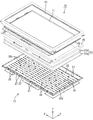
- FIG. 1 is an exploded perspective view of a television receiver TV according to Embodiment 1.
- FIG. An exploded perspective view of the liquid crystal display device 10 is shown.
- a cross-sectional view along the long side direction of the liquid crystal panel 11 is shown.
- An enlarged plan view of the array substrate 11b is shown.
- An enlarged plan view of the CF substrate 11a is shown.
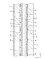
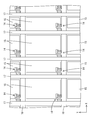
- FIG. 2 shows a cross-sectional view of the liquid crystal display device 10 along the short side direction.
- FIG. 2 shows a cross-sectional view along the long side direction of the liquid crystal display device 10.
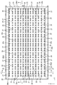
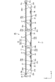
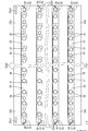
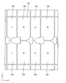
- FIG 3 is a plan view showing an arrangement configuration of a bottom plate 22a of the chassis 22 and the first connector 31 and the second connector 32 on each LED board 25.
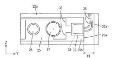
- the enlarged plan view showing the connection aspect of the 2nd connector 32 connected to the edge part 25b provided with the end surface 25a of the LED board 25, and the 1st connector 31 on this edge part 25b is shown.
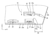
- the expanded sectional view showing the connection direction of the 2nd connector 32 connected to the edge part 25b provided with the end surface 25a of the LED board 25, and the 1st connector 31 on this edge part 25b is shown.
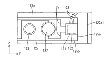
- the enlarged plan view showing the connection aspect of the 2nd connector 132 connected to the edge part 125b provided with the end surface 125a of the LED board 125 in Embodiment 2 and the 1st connector 131 on this edge part 125b is shown. It is sectional drawing along the short side direction of the baseplate 222a, Comprising: The edge part 225b provided with the one end surface 225a of LED board 225 in Embodiment 3, and the 2nd connector connected to the 1st connector 231 on this edge part 225b
- the expanded sectional view showing the connection aspect and connection direction of 232 is shown.
- the expanded sectional view showing the connection direction of the edge part 325b provided with the end surface 325a of the LED board 325 in Embodiment 4, and the 2nd connector 332 connected to the 1st connector 331 on this edge part 325b is shown.
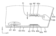
- curd connector 432 connected to the edge part 425b provided with the one end surface 425a of LED board 425 in Embodiment 5, and the terminal part 431 on this edge part 425b is shown.
- curd connector 532 connected to the terminal part 531 on this edge part 525b is shown.
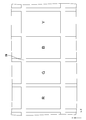
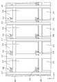
- An enlarged plan view of a CF substrate according to Modification 1 is shown.
- An enlarged plan view of a CF substrate according to Modification 2 is shown.
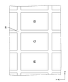
- An enlarged plan view of a CF substrate according to Example 3 is shown.
- An enlarged plan view of a CF substrate according to modification 4 is shown.
- An enlarged plan view of a CF substrate according to Modification 5 is shown.
- An enlarged plan view of a CF substrate according to Modification 6 is shown.
- An enlarged plan view of an array substrate according to Modification 6 is shown.
- An enlarged plan view of a CF substrate according to Modification 7 is shown.
- An enlarged plan view of a CF substrate according to Modification 8 is shown.
- An enlarged plan view of an array substrate according to Modification 8 is shown.
- An enlarged plan view of a CF substrate according to Modification 9 is shown.
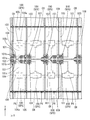
- An enlarged plan view of an array substrate according to Modification 10 is shown.
- Embodiment 1 will be described with reference to the drawings.
- the liquid crystal display device 10 is illustrated.
- a part of each drawing shows an X axis, a Y axis, and a Z axis, and each axis direction is drawn to be a direction shown in each drawing.
- the upper side shown in FIG.2 and FIG.3 be a front side, and let the lower side of the figure be a back side.
- the television receiver TV includes a liquid crystal display device 10 that is a display device, front and back cabinets Ca and Cb that are accommodated so as to sandwich the liquid crystal display device 10, and power supply.
- Power supply circuit board P a tuner (receiving unit) T capable of receiving a TV image signal, an image conversion circuit board VC for converting the TV image signal output from the tuner T into an image signal for the liquid crystal display device 10
- a stand S a stand S.
- the liquid crystal display device 10 has a horizontally long (longitudinal) rectangular shape (rectangular shape) as a whole, the long side direction is the horizontal direction (X-axis direction), and the short side direction is the vertical direction (Y-axis direction, vertical direction). They are housed in a matched state. As shown in FIG. 2, the liquid crystal display device 10 includes a liquid crystal panel 11 that is a display panel and a backlight device (an example of a lighting device) 12 that is an external light source. It is designed to be held together.
- the configuration of the liquid crystal panel 11 in the liquid crystal display device 10 will be described.
- the liquid crystal panel 11 has a horizontally long (longitudinal) rectangular shape (rectangular shape) as a whole.
- a pair of transparent (translucent) glass substrates 11a and 11b And a liquid crystal layer 11c containing liquid crystal, which is a substance whose optical characteristics change with application of an electric field.
- the substrates 11a and 11b maintain a gap corresponding to the thickness of the liquid crystal layer. In the state, they are bonded together by a sealing agent (not shown).
- polarizing plates 11d and 11e are attached to the outer surface sides of both the substrates 11a and 11b, respectively. Note that the long side direction of the liquid crystal panel 11 coincides with the X-axis direction, and the short side direction coincides with the Y-axis direction.
- the front side is the CF substrate 11a
- the back side is the array substrate 11b.
- TFTs Thin Film Transistors
- pixel electrodes 15 which are switching elements are matrixed.
- a large number of gate wirings 16 and source wirings 17 are arranged around the TFTs 14 and the pixel electrodes 15 so as to surround the TFTs 14 and the pixel electrodes 15.
- the pixel electrode 15 has a vertically long (longitudinal) rectangular shape (rectangular shape) in which the long side direction coincides with the Y-axis direction and the short side direction coincides with the X-axis direction. It consists of a transparent electrode such as (Zinc Oxide).
- the gate wiring 16 and the source wiring 17 are connected to the gate electrode and the source electrode of the TFT 14, respectively, and the pixel electrode 15 is connected to the drain electrode of the TFT 14. Further, an alignment film 18 for aligning liquid crystal molecules is provided on the TFT 14 and the pixel electrode 15 on the liquid crystal layer 11c side, as shown in FIG.
- a terminal portion led out from the gate wiring 16 and the source wiring 17 is formed at an end portion of the array substrate 11b, and a driver component for driving a liquid crystal (not shown) is connected to the anisotropic conductive film (not shown). Crimp connection is made through ACF (Anisotropic Conductive Film), and the driver components for driving the liquid crystal are electrically connected to a display control circuit board (not shown) through various wiring boards.
- This display control circuit board is connected to an image conversion circuit board VC (see FIG. 1) in the television receiver TV, and based on an output signal from the image change circuit board VC, each wiring 16, 17 is connected via a driver component. It is assumed that a drive signal is supplied to.
- a color filter 19 in which the portions R, G, B, and Y are arranged in a matrix (matrix) is provided.
- the color filter 19 according to the present embodiment includes a yellow colored portion Y in addition to a red colored portion R, a green colored portion G, and a blue colored portion B that are the three primary colors of light.
- the colored portions R, G, B, and Y selectively transmit light of each corresponding color (each wavelength).
- Each colored portion R, G, B, Y has a vertically long (longitudinal) rectangular shape (rectangular shape) in which the long side direction coincides with the Y-axis direction and the short side direction coincides with the X-axis direction, like the pixel electrode 15. I am doing.
- a lattice-shaped light shielding layer (black matrix) BM is provided to prevent color mixing.
- a counter electrode 20 and an alignment film 21 are sequentially stacked on the color filter 19 on the CF substrate 11 a on the liquid crystal layer 11 c side.
- the colored portions R, G, B, and Y constituting the color filter 19 will be described in detail.
- the colored portions R, G, B, and Y are arranged in a matrix with the X-axis direction as the row direction and the Y-axis direction as the column direction.
- Y have the same dimension in the column direction (Y-axis direction), but the dimension in the row direction (X-axis direction) is different for each colored portion R, G, B, Y.
- the colored portions R, G, B, and Y are arranged in the row direction in the order of the red colored portion R, the green colored portion G, the blue colored portion B, and the yellow colored portion Y from the left side shown in FIG.
- the red colored portion R and the blue colored portion B in the row direction are relatively larger than the yellow colored portion Y and the green colored portion G in the row direction. It is said. That is, the colored portions R and B having relatively large dimensions in the row direction and the colored portions G and Y having relatively small dimensions in the row direction are alternately and repeatedly arranged in the row direction. Thereby, the area of the red coloring part R and the blue coloring part B is made larger than the areas of the green coloring part G and the yellow coloring part Y. The areas of the blue colored portion B and the red colored portion R are equal to each other. Similarly, the areas of the green colored portion G and the yellow colored portion Y are equal to each other. 3 and 5 show a case where the areas of the red colored portion R and the blue colored portion B are about 1.6 times the areas of the yellow colored portion Y and the green colored portion G. Show.
- the dimension in the row direction (X-axis direction) of the pixel electrode 15 varies from column to column. . That is, among the pixel electrodes 15, the size and area in the row direction of the pixel electrode 15 that overlaps with the red color portion R and the blue color portion B are the same as those in the row direction of the pixel electrode 15 that overlaps with the yellow color portion Y and the green color portion G. It is relatively larger than the size and area.
- the gate wirings 16 are all arranged at an equal pitch, while the source wirings 17 are arranged at two different pitches depending on the dimensions of the pixel electrodes 15 in the row direction.
- the liquid crystal display device 10 uses the liquid crystal panel 11 including the color filter 19 including the four colored portions R, G, B, and Y, as shown in FIG.
- the television receiver TV is provided with a dedicated image conversion circuit board VC. That is, the image conversion circuit board VC converts the television image signal output from the tuner T into an image signal of each color of blue, green, red, and yellow, and outputs the generated image signal of each color to the display control circuit board. can do. Based on this image signal, the display control circuit board drives the TFTs 14 corresponding to the pixels of each color in the liquid crystal panel 11 via the wirings 16 and 17, and transmits the colored portions R, G, B, and Y of each color. The amount of light can be appropriately controlled.
- the backlight device 12 is arranged so as to cover a substantially box-shaped chassis 22 having a light output part 22d on the light output surface side (liquid crystal panel 11 side), and a light output part 22d of the chassis 22. And an optical member 23 that is disposed along the outer edge of the chassis 22 and that holds the outer end of the optical member 23 between the chassis 22 and the frame 26. Further, in the chassis 22, the LED 24 arranged opposite to the position directly below the optical member 23 (the liquid crystal panel 11), the LED board 25 on which the LED 24 is mounted, and a position corresponding to the LED 24 on the LED board 25. And a diffusing lens 27 attached to the lens.
- the backlight device 12 is a so-called direct type.
- a holding member 28 that can hold the LED substrate 25 between the chassis 22 and a reflection sheet 29 that reflects the light in the chassis 22 toward the optical member 23 are provided. . Subsequently, each component of the backlight device 12 will be described in detail.
- the chassis 22 is made of metal. As shown in FIGS. 6 to 8, the chassis 22 has a horizontally long bottom (rectangular, rectangular) as in the liquid crystal panel 11, and each side (a pair of bottom plates 22a). It consists of a side plate 22b that rises from the outer ends of the long side and a pair of short sides toward the front side (light emission side), and as a whole, has a shallow substantially box shape that opens toward the front side. Further, the bottom plate 22a of the chassis 22 includes a first end side 22a1 which is an end side of a pair of short sides and a second end side 22a2 which is an end side of a pair of long sides ( (See FIG. 9).
- the long side direction of the chassis 22 coincides with the X-axis direction (horizontal direction), and the short side direction coincides with the Y-axis direction (vertical direction).
- a frame 26 and an optical member 23 to be described below can be placed on each receiving plate 22c in the chassis 22 from the front side.
- a frame 26 is screwed to each receiving plate 22c.
- An attachment hole 22 d for attaching the holding member 28 is provided in the bottom plate 22 a of the chassis 22.
- a plurality of mounting holes 22d are arranged in a distributed manner corresponding to the mounting position of the holding member 28 in the bottom plate 22a.
- the optical member 23 has a horizontally long rectangular shape in a plan view, like the liquid crystal panel 11 and the chassis 22. As shown in FIGS. 7 and 8, the optical member 23 has its outer edge portion placed on the receiving plate 22c so as to cover the light output portion 22d of the chassis 22, and between the liquid crystal panel 11 and the LED 24 (LED substrate 25). Arranged between them.
- the optical member 23 includes a diffusion plate 23a disposed on the back side (the LED 24 side, opposite to the light emitting side) and an optical sheet 23b disposed on the front side (the liquid crystal panel 11 side, the light emitting side). .
- the diffusing plate 23a has a structure in which a large number of diffusing particles are dispersed in a substrate made of a substantially transparent resin having a predetermined thickness and has a function of diffusing transmitted light.
- the optical sheet 23b has a sheet shape that is thinner than the diffusion plate 23a, and two optical sheets 23b are laminated. Specific types of the optical sheet 23b include, for example, a diffusion sheet, a lens sheet, a reflective polarizing sheet, and the like, which can be appropriately selected and used.
- the frame 26 has a frame shape along the outer peripheral edge portions of the liquid crystal panel 11 and the optical member 23. An outer edge portion of the optical member 23 can be sandwiched between the frame 26 and each receiving plate 22c (see FIGS. 7 and 8).
- the frame 26 can receive the outer edge portion of the liquid crystal panel 11 from the back side, and can sandwich the outer edge portion of the liquid crystal panel 11 with the bezel 13 arranged on the front side (FIGS. 7 and 8). reference).
- the LED 24 is a so-called top type that is mounted on the LED substrate 25 and has a light emitting surface on the surface opposite to the mounting surface with respect to the LED 24.
- the LED 24 includes an LED chip 24a that emits blue light as a light source, and includes a green phosphor and a red phosphor as phosphors that emit light when excited by blue light.
- the LED 24 has a configuration in which an LED chip 24 a made of, for example, an InGaN-based material is sealed with a resin material on a substrate portion fixed to the LED substrate 25.
- the LED chip 24a mounted on the substrate part has a main emission wavelength in the range of 420 nm to 500 nm, that is, in the blue wavelength region, and can emit blue light (blue monochromatic light) with excellent color purity. It is said.
- As a specific main emission wavelength of the LED chip 24a for example, 451 nm is preferable.
- the resin material that seals the LED chip 24a is excited by the green phosphor that emits green light when excited by the blue light emitted from the LED chip 24a and the blue light emitted from the LED chip 24a.
- a red phosphor emitting red light is dispersed and blended at a predetermined ratio.
- the LED 24 can emit light of a predetermined color as a whole, for example, white or blueish white. Since yellow light is obtained by synthesizing the green component light from the green phosphor and the red component light from the red phosphor, the LED 24 is composed of the blue component light from the LED chip 24a and the yellow light. It can be said that it also has the light of the component.
- the chromaticity of the LED 24 varies depending on, for example, the absolute value or relative value of the content of the green phosphor and the red phosphor, and accordingly the content of the green phosphor and the red phosphor is adjusted as appropriate. Thus, the chromaticity of the LED 24 can be adjusted.
- the green phosphor has a main emission peak in the green wavelength region of 500 nm to 570 nm
- the red phosphor has a main emission peak in the red wavelength region of 600 nm to 780 nm. It is said.
- the green phosphor and the red phosphor provided in the LED 24 will be described in detail.
- ⁇ -SiAlON which is a kind of sialon phosphor
- the sialon-based phosphor is a substance in which a part of silicon atoms of silicon nitride is replaced with aluminum atoms and a part of nitrogen atoms with oxygen atoms, that is, a nitride.
- a sialon phosphor, which is a nitride has excellent luminous efficiency and durability compared to other phosphors made of, for example, sulfide or oxide.
- “excellent in durability” specifically means that, even when exposed to high-energy excitation light from an LED chip, the luminance does not easily decrease over time.
- Rare earth elements for example, Tb, Yg, Ag, etc.
- ⁇ -SiAlON which is a kind of sialon-based phosphor, has a general formula Si6-ZAlZOZN: Eu (z indicates a solid solution amount) or (Si, Al) 6 in which aluminum and oxygen are dissolved in ⁇ -type silicon nitride crystal. (O, N) 6: a substance represented by Eu.
- the ⁇ -SiAlON for example, Eu (europium) is used as an activator, and thereby the color purity of green light, which is fluorescent light, is particularly high. It is extremely useful in adjusting On the other hand, as the red phosphor, it is preferable to use casoon, which is a kind of cascading phosphor.
- Cousin-based phosphors are nitrides containing calcium atoms (Ca), aluminum atoms (Al), silicon atoms (Si), and nitrogen atoms (N). For example, other phosphors made of sulfides, oxides, etc. In comparison, it is excellent in luminous efficiency and durability.
- the cascading phosphor uses rare earth elements (for example, Tb, Yg, Ag, etc.) as an activator.
- Casun which is a kind of cousin phosphor, uses Eu (europium) as an activator and is represented by the composition formula CaAlSiN3: Eu.
- the LED substrate 25 has a base material that is horizontally long when viewed in a plane.
- the long side direction coincides with the X axis direction
- the short side direction coincides with the Y axis direction.
- the chassis 22 is accommodated while extending along the bottom plate 22a.
- the LED 24 is surface-mounted on the surface facing the front side (the surface facing the optical member 23 side).
- the LED 24 has a light emitting surface facing the optical member 23 (the liquid crystal panel 11) and an optical axis that coincides with the Z-axis direction, that is, the direction orthogonal to the display surface of the liquid crystal panel 11.
- a plurality of LEDs 24 are linearly arranged in parallel along the long side direction (X-axis direction) of the LED substrate 25, and a wiring pattern (an example of connection wiring) 35 formed on the LED substrate 25 (FIG. 9). Are connected in series.
- the arrangement pitch of the LEDs 24 is substantially constant, that is, it can be said that the LEDs 24 are arranged at substantially equal intervals.
- the LED substrate 25 having the above-described configuration is arranged in parallel in the chassis 22 in a state where the long side direction and the short side direction are aligned with each other in the X-axis direction and the Y-axis direction. ing. That is, the LED substrate 25 and the LED 24 mounted thereon are both set in the X-axis direction (the long side direction of the chassis 22 and the LED substrate 25) in the chassis 22 and in the Y-axis direction (the chassis 22 and the LED substrate 25).
- the short side direction is arranged in a matrix with the column direction (arranged in a matrix, planar arrangement).
- a total of 28 LED substrates 25 are arranged in parallel in the chassis 22, two in the X-axis direction and 14 in the Y-axis direction.
- an end portion on the outer edge side of the chassis 22 is connected to a first connector (first
- An example of a connection member 31 and a second connection connector (an example of a second connection member) 32 are provided.
- the second connector 32 is electrically connected to the external LED drive circuit side connector portion via the power supply wiring 38, so that power is supplied to each LED 24 and the drive of each LED 24 can be controlled. It is said.
- the arrangement pitch of the LED substrates 25 arranged along the Y-axis direction is substantially equal. Therefore, it can be said that the LEDs 24 arranged in a plane along the bottom plate 22a in the chassis 22 are arranged at approximately equal intervals in the X-axis direction and the Y-axis direction.
- the base material of the LED substrate 25 is made of the same metal as the chassis 22 such as an aluminum material, and the above-described wiring pattern 35 made of a metal film such as a copper foil is formed on the surface thereof via an insulating layer.
- the outermost surface has a structure in which a reflective layer (not shown) exhibiting white having excellent light reflectivity is formed.
- the LEDs 24 arranged in parallel on the LED substrate 25 are connected in series by the wiring pattern 35.
- insulating materials such as a ceramic.
- the diffusing lens 27 is made of a synthetic resin material (for example, polycarbonate, acrylic, etc.) that is substantially transparent (having high translucency) and has a refractive index higher than that of air. As shown in FIGS. 6 to 8, the diffusion lens 27 has a predetermined thickness and is formed in a substantially circular shape when viewed from above, and covers each LED 24 individually from the front side with respect to the LED substrate 25. That is, each LED 24 is attached so as to overlap with each other when seen in a plan view.
- the diffusing lens 27 can emit light having strong directivity emitted from the LED 24 while diffusing.
- the diffusing lens 27 is disposed at a position that is substantially concentric with the LED 24 in a plan view. In FIG. 7, since the cross-sectional configuration of the holding member 28 is illustrated, the side surface of the diffusing lens 27 disposed on the back side of the drawing is illustrated.
- the holding member 28 will be described.
- the holding member 28 is made of a synthetic resin such as polycarbonate, and has a white surface with excellent light reflectivity. As shown in FIGS. 6 to 8, the holding member 28 is fixed to the chassis 22 by protruding from the main body 28 a toward the back side, that is, the chassis 22 side, along the main body 28 a along the plate surface of the LED substrate 25. Part 28b.
- the main body 28 a has a substantially circular plate shape in plan view, and at least the LED board 25 can be sandwiched between the main body 28 a and the bottom plate 22 a of the chassis 22.
- the fixing portion 28b can be locked to the bottom plate 22a while penetrating the insertion holes 25b and the attachment holes respectively formed corresponding to the mounting positions of the holding member 28 on the LED board 25 and the bottom plate 22a of the chassis 22. .
- a plurality of the holding members 28 are appropriately distributed in the plane of the LED substrate 25b, and are arranged at positions adjacent to the diffusion lens 27 (LED 24) in the X-axis direction. Yes.
- the holding member 28 sandwiches the LED board 25 between the main body 25a and the bottom plate 22a of the chassis 22 without the bottom 29a of the reflection sheet 29 (first).
- 1 holding member and a member (second holding member) that sandwiches the bottom portion 29a of the reflection sheet 29 together with the LED substrate 25 between the main body portion 25a and the bottom plate 22a of the chassis 22 are included.
- the holding member 28 (second holding member) that holds the bottom 29a of the reflection sheet 29 together with the LED substrate 25 is provided with a support portion 28c that protrudes from the main body portion 28a to the front side, and the support portion 28c. Two types are included.
- the support portion 28c can support the optical member 23 (directly the diffusion plate 23a) from the back side, thereby maintaining a constant positional relationship between the LED 24 and the optical member 23 in the Z-axis direction. And inadvertent deformation of the optical member 23 can be restricted.
- the reflection sheet 29 is made of a synthetic resin, and the surface thereof is white with excellent light reflectivity. As shown in FIGS. 6 to 8, the reflection sheet 29 has a size that is laid over almost the entire inner surface of the chassis 22, so that all the LED boards 25 arranged in parallel in the chassis 22 are arranged. Covering from the front side is possible. The reflection sheet 29 can efficiently raise the light in the chassis 22 toward the optical member 23 side.
- the reflection sheet 29 extends along the bottom plate 22a of the chassis 22 and covers a large portion of the bottom plate 22a.
- the reflection sheet 29 rises from the outer edge on the short side of the bottom portion 29a to the front side and rises from the bottom portion 29a.
- the bottom portion 29a of the reflection sheet 29 is arranged so as to be on the front side with respect to the front side surface of each LED substrate 25, that is, the mounting surface of the LED 24.
- the bottom 29a of the reflection sheet 29 is provided with a lens insertion hole 29d through which each diffusion lens 27 is inserted at a position overlapping each diffusion lens 27 (each LED 24) in plan view.
- the bottom portion 29a is provided with a holding member insertion hole for passing the fixing portion 28b at a position overlapping with each holding member 28 in plan view, and particularly holds the LED substrate 25 without passing through the bottom portion 29a.
- the holding member insertion hole corresponding to the holding member 28 (first holding member) is set to a size that allows the main body portion 28a to pass therethrough.
- the color filter 19 of the liquid crystal panel 11 includes a yellow colored portion in addition to the colored portions R, G, and B, which are the three primary colors of light, as shown in FIGS. Since Y is included, the color gamut of the display image displayed by the transmitted light is expanded, so that it is possible to realize display with excellent color reproducibility. In addition, since the light transmitted through the yellow colored portion Y has a wavelength close to the peak of visibility, the human eye tends to perceive brightly even with a small amount of energy. Thereby, even if it suppresses the output of LED24 which the backlight apparatus 12 has, sufficient brightness
- the display image of the liquid crystal panel 11 tends to be yellowish as a whole.
- the chromaticity in the LED 24 is adjusted to a blue color that is a complementary color of yellow, thereby correcting the chromaticity in the display image.
- the LED 24 of the backlight device 12 has the main emission wavelength in the blue wavelength region and the highest light emission intensity in the blue wavelength region. ing.
- the area ratio of the blue colored portion B constituting the color filter 19 is set to be relatively larger than that of the green colored portion G and the yellow colored portion Y, whereby the color filter
- the 19 transmitted light can contain more blue light which is a complementary color of yellow.
- the brightness of the red light among the light emitted from the liquid crystal panel 11 is lowered. This is because, in the four primary color type liquid crystal panel 11, compared to the three primary color type, the number of subpixels constituting one pixel increases from three to four, so the area of each subpixel decreases. It is presumed that the brightness of the red light is particularly lowered due to this.
- the area ratio of the red colored portion R constituting the color filter 19 is set to be relatively larger than that of the green colored portion G and the yellow colored portion Y, whereby the color filter
- the transmitted light of 19 can contain a larger amount of red, and therefore, it is possible to suppress a decrease in lightness of the red light caused by the color filter 19 having four colors.
- the fitting mode and the connection mode of the power supply wiring 38 will be described in detail.
- the configuration and connection mode of the wiring pattern 35 and the first connector 31 provided on the LED substrate 25 will be described.
- the wiring pattern 35 extends in a meandering manner on the LED substrate 25 and connects the LEDs 24 in series.
- the first connector 31 has a rectangular shape in plan view, and is arranged such that the plate surface directions of the side surfaces thereof coincide with the X-axis direction and the Y-axis direction, respectively.
- the first connector 31 on the LED board 25 is a side plate 22b (of the chassis 22) that rises from the first end side 22a1 of the bottom plate 22a among both end faces (both end faces in the longitudinal direction) on the short side of the LED board 25.
- the LED substrate 25 is disposed on an end portion 25b having an end surface 25a facing the outer side (see FIG. 10). Both ends of the wiring pattern 35 are electrically connected to the first connector 31 on the end portion 25b.
- the second connector 32 has a rectangular shape like the first connector 31 in plan view, and the plate surface directions of the side surfaces thereof are the X-axis direction and the Y-axis direction, respectively. They are arranged to match.
- Each second connector 32 is connected to the first connector 31 from the front side (the light output part 22d side of the chassis 22) as shown in FIG.
- the second connector 32 is connected to the first connector 31 in a direction D1 (see FIG. 10) that overlaps the first connector 31 in plan view.
- the second connector has a rectangular shape that is slightly larger than the first connector, and a frame-shaped accommodation recess 32a is provided inside the second connector (FIG. 11). reference). Then, by bringing the second connector 32 closer to the first connector 31 from the front side, the opening edge 31a of the first connector 31 is accommodated in the accommodating recess 32a of the second connector 32, whereby the first connector 31 and the second connector 31 are The connector 32 is fitted and fixed.
- metal first connector side terminal portions 41 that are electrically connected to both ends of the wiring pattern 35 are provided.
- a metal second connector side terminal portion 42 electrically connected to the power supply wiring 38 is provided inside the second connector 32.
- the opening edge part 31a of the 1st connector 31 is accommodated in the accommodation recessed part 32a of the 2nd connector 32, and the 2nd connector side terminal part 42 contact
- the first connector 31 and the second connector 32 are electrically connected.
- the power supply wiring 38 is electrically connected to the second connector, and extends from the side surface of the second connector 32 facing the side plate rising from the first end side 22a1, as shown in FIG.
- the power supply wiring 38 extending from the side surface 32c of the second connector 32 is routed toward the wiring insertion hole 22a3 (see FIG. 9) provided on the second end side 22a2 side of the bottom plate 22a in the chassis 22.
- the power supply wiring 38 routed to the wiring insertion hole 22a3 is inserted into the wiring insertion hole 22a3 and routed to the back side of the chassis 22, and is electrically connected to the connector portion on the LED drive circuit side on the back side of the chassis 22. Has been.
- the power supply wiring 38 and the wiring pattern 35 are electrically connected via the first connector 31 and the second connector 32. Electric power is supplied from the LED drive circuit to each LED 24. 9 and 11, only the vicinity of the portion connected to the second connector 32 of the power supply wiring 38 is illustrated, and the other portions are not illustrated.
- the second connector 32 is connected to the first connector 31 with the direction D1 as the connection direction, the second connector 32 is positioned so as to overlap the first connector 31, as shown in FIG. Since the first connector 31 is disposed, the first connector 31 is not disposed on the side facing the side plate 22b on the short side of the chassis 22 (exposed to the first end 22a1 side). In such a configuration, as shown in FIGS. 9 to 11, since the second connector 32 is not disposed between the first end side 22a1 and the one end face 25a of the LED substrate 25, the first end side 22a1 can be brought closer to the one end surface 25a side of the LED substrate 25, and the distance W1 between the first end side 22a1 and the one end surface 25a of the LED substrate 25 can be reduced.
- the backlight device 12 compared with the case where the second connector 32 is arranged on the side surface exposed to the first end side 22a1 side of the side surface of the first connector 31, the second plate 32a of the bottom plate 22a.
- the distance W1 between the one end 22a1 (the side plate 22b on the short side of the chassis 22) and the one end face 25a of the LED board 25 is narrowed (see FIGS. 10 and 11). Thereby, in the backlight device 12, the frame is narrowed.
- the second connector 32 connected to the first connector 31 overlaps the first connector 31 in a plan view. It is possible to prevent the second connector 32 from being arranged between the one end face 25a of the substrate 25. For this reason, even if the side plate 22b of the chassis 22 facing the one end face 25a of the LED board 25 is brought close to the one end face 25a side (inside the chassis 22), the second connector 32 does not get in the way, and The side plate of the chassis 22 more than the case where the second connector 32 is connected to the first connector 31 with the direction extending from the first end side 22a1 to the one end surface 25a orthogonal to the first end side 22a1 facing the end surface 25a.
- the distance W1 between 22b and the one end surface 25a of the LED substrate 25 can be relatively narrowed. Thereby, the frame of the backlight apparatus 12 can be narrowed.
- the second connector 32 is connected to the first connector 31 from a direction overlapping the first connector 31 in plan view. Therefore, when connecting the second connector 32 to the first connector 31, the second connector 32 can be positioned in advance so as to overlap the first connector 31 in a plan view. Thus, the second connector 32 can be easily connected.
- the bottom plate 22a has a horizontally long rectangular shape, and its end sides are a pair of first end sides 22a1 along the short side direction of the bottom plate 22a and the bottom plate 22a.
- a plurality of LED substrates 25 are arranged on the bottom plate 22a, and each of the one end faces 25a rises from the first end side 22a1.
- the first connector 31 is arranged on each of the plurality of LED boards 25 and the second connector 32 is connected to each of the plurality of first connectors 31.
- the distance W1 between the side plate 22b rising from the first end side 22a1 and the one end surface 25a of the LED substrate 25 can be reduced. Further, it is possible to reduce the frame of the backlight device 12.
- each of the plurality of LED substrates 25 has a horizontally long rectangular shape, and its long sides so that both end surfaces on the short side are along the first end side 22a1. Both end surfaces on the side are arranged in a matrix on the bottom plate 22a along the second end side 22a2, and one of the end surfaces on the short side is an end surface 25a. Therefore, it is possible to reduce the frame of the backlight device 12 while realizing the backlight device 12 having a configuration in which the plurality of LED substrates 25 are arranged in a matrix in the chassis 22.
- the backlight device 12 further includes a diffusing lens 27 that is disposed on each of the plurality of LED substrates 25, covers the light emitting side of the LED 24, and diffuses the light from the LED 24.
- a diffusing lens 27 that is disposed on each of the plurality of LED substrates 25, covers the light emitting side of the LED 24, and diffuses the light from the LED 24.
- the backlight device 12 includes a bottom portion 29a laid on the LED substrate 25, a lens insertion hole 29d provided on the bottom portion 29a and through which the diffusion lens 27 is inserted, and a side plate 22b of the chassis 22. Further, a reflection sheet 29 having rising portions 29b1 and 29b2 rising on the light output portion 22d side (front side) of the chassis 22 on the side is further provided. Of the plurality of second connectors 32, the second connector 32 disposed closest to the second end side 22a2 is disposed between the reflection sheet 29 and the side plate 22b rising from the first end side 22a1. .
- the light emitted from the LED 24 and directed toward the rising portions 22b1 and 22b2 of the reflection sheet 29 is not blocked by the first connector 31 and the second connector 32, thereby increasing the utilization efficiency of the light emitted from the LED 24. be able to.
- connection direction of the power supply wiring 138 to the second connector 132 is different from that in the first embodiment. Since other configurations are the same as those of the first embodiment, description of the structure, operation, and effect is omitted.
- FIG. 12 the part obtained by adding the numeral 100 to the reference sign in FIG. 10 is the same as the part described in the first embodiment.
- the power supply wiring 138 is connected to the side surface exposed to the second end side 122 a 2 among the side surfaces of the first connector 131. It extends in parallel with 122a1. That is, the power supply wiring 138 is connected to the second connector 132 with the direction parallel to the second end side 122a2 as the connection direction. For this reason, the power supply wiring 138 is connected to the second connector with the direction from the first end 122a1 side toward the one end face 125a of the LED substrate 125 sandwiching the first connector 131 so as to be orthogonal to the second end 122a1.
- the power supply wiring 138 can be hardly routed to the LED side (diffuse lens 127 side). As a result, when the power supply wiring 138 is routed in the chassis, it is possible to prevent or suppress the power supply wiring 138 from being routed to the light emission side of the LED (the light emission side of the diffusion lens 127).
- Embodiment 3 will be described with reference to the drawings.
- the third embodiment is different from the first embodiment in the configuration of the second connector 232 and the connection mode of the second connector 232 to the first connector 231. Since other configurations are the same as those of the first embodiment, description of the structure, operation, and effect is omitted.
- FIG. 13 the part obtained by subtracting the numeral 200 from the reference sign of each part is the same as the part described in the first embodiment.
- the second connector 232 has a linear shape along a direction parallel to the first end side (Y-axis direction).
- the second connector 232 has a fitting recess 232 a that opens toward the first connector 231 when the second connector 232 is arranged on the front side of the first connector 231 and can be fitted to the first connector 231. Is provided.
- the fitting recess 232a overlaps each first connector 231 on each LED board 225 (see FIG. 9) in which the second connector 232 is arranged in parallel along the direction (Y-axis direction) parallel to the first end side. When arranged along the direction parallel to the first end side (Y-axis direction), each is provided at a position overlapping each first connector 231.
- each first connector 231 is fitted to each fitting recess 232 a on the second connector 232.
- the second connectors 232 are electrically connected to the first connectors 231 simultaneously.
- the backlight device since one second connector 232 can be connected simultaneously with the plurality of first connectors 231, connection work between the first connector 231 and the second connector 232 is simplified. Can be.
- the number of second connectors 232 connected to the first connector 231 can be reduced, the number of power supply wirings 238 can be reduced. As a result, the proportion of the power supply wiring 238 in the chassis can be reduced, and the frame of the backlight device can be further narrowed.
- connection mode of the second connector 332 to the first connector 331 is different from that of the first embodiment. Since other configurations are the same as those of the first embodiment, description of the structure, operation, and effect is omitted.
- FIG. 14 the part obtained by adding the numeral 300 to the reference numeral in FIG. 11 is the same as the part described in the first embodiment.
- the second connector 332 is on the front side (the light emitting part side of the chassis 322) with respect to the first connector 331, and is one end surface 325 a of the LED substrate 325.
- the side plate 322b facing each other is connected to the first connector 331 with the direction D2 from the opposite side toward the first connector 331 across the first connector 331 as a connection direction. That is, the second connector 332 is connected to the first connector 331 from obliquely above the first connector 331.
- the opening edge part 331a of the 1st connector 331 demonstrated in Embodiment 1 and the accommodation recessed part 332a of the 2nd connector 332 are also inclined and provided along said direction D2, as shown in FIG. .
- the second connector 332 By bringing the second connector 332 closer to the first connector 331 along the direction D2, the opening edge 331a of the first connector 331 is accommodated in the accommodation recess 332a of the second connector 332, and the first connector 331 is obtained. And the second connector 332 can be fitted.
- the second connector 332 is connected to the first connector 331 using the direction D2 as the connection direction, so that in the backlight device according to the present embodiment, the second connector is connected to the first connector 331.
- the side plate 322b facing the one end surface 325a of the LED substrate 325 does not get in the way. For this reason, the second connector 332 can be easily connected to the first connector 331.
- Embodiment 5 will be described with reference to the drawings.
- the configuration of the connecting member is different from that of the first embodiment. Since other configurations are the same as those of the first embodiment, description of the structure, operation, and effect is omitted. 15 and 16, the part obtained by adding the numeral 400 to the reference numerals in FIGS. 10 and 11 is the same as the part described in the first embodiment.
- the end portion 425b including one end surface 425a facing the first end surface 422a1 of the bottom plate 422a of the chassis among the both ends in the long side direction of the LED substrate 425
- a terminal portion (an example of a first connecting member) 431 that is rectangular in plan view is provided.
- An exposed electrode terminal 431a is provided on the terminal portion 431, and both ends of a wiring pattern 435 provided on the LED substrate 425 are electrically connected to the electrode terminal 431a.
- a card type card connector (an example of a second connecting member) 432 having a rectangular shape in a plan view as shown in FIG. 15 is connected to the terminal portion 431.
- the card connector 432 is arranged so that the plate surface directions of the side surfaces thereof coincide with the X-axis direction and the Y-axis direction, respectively.
- the card connector 432 is connected to the terminal portion 431 from the front side (the light emitting portion side of the chassis 422), as in the first embodiment. That is, as shown in FIGS. 15 and 16, the second connector 432 is connected to the terminal portion 431 from a direction D1 (see FIG. 11) that overlaps the terminal portion 431 in plan view.
- the power supply wiring 438 is electrically connected to the card connector 432, and as shown in FIG. 15, the side plate rising from the first end 422a1 among the side surfaces of the card connector 432, as in the first embodiment. It extends from the opposite side.
- the card connector 432 has a rectangular shape that is slightly larger than the terminal portion 431 in a plan view, and a fitting recess 431 a is provided inside the card connector 432.
- a metal contact portion 432 is provided on the bottom surface of the fitting recess 431a.
- the first end 422a1 of the bottom plate 422a and the one end surface 425a of the LED board 425 are compared with the case where the card connector 432 is disposed on the one end surface 425a side facing the first end surface 422a1. Since the distance between the two is reduced, it is possible to narrow the frame of the backlight device.
- first connector and the second connector are illustrated as having a rectangular shape in plan view.
- shapes and configurations of the first connector and the second connector are not limited.
- the configuration in which the one end surface of the LED substrate faces the side plate rising from the first end side of the chassis is exemplified.
- the one end surface of the LED substrate faces the side plate rising from the second end side of the chassis. It is good also as a structure.
- the LED substrate has a horizontally long rectangular shape, the short side thereof coincides with the first end side, and the long side thereof coincides with the configuration. The number is not limited.
- the configuration in which the LEDs are arranged in a line along the long side direction (X-axis direction) of the chassis on the LED substrate is exemplified.
- the shape, arrangement, number, etc. of the LEDs Is not limited.
- the LED may be arranged side by side along the short side direction (Y-axis direction) of the chassis.
- the configuration in which the one end surface of the LED substrate is a flat surface is illustrated.
- the one end surface of the LED substrate may be a curved surface having a roundness.
- the configuration in which the one end surface of the LED substrate is parallel to the first end side of the chassis (the side plate rising from the end side) is exemplified, but the configuration may not be parallel.
- connection direction of the second connector with respect to the first connector can be changed as appropriate.
- the arrangement order of the colored portions R, G, B, and Y in the color filter can be changed as appropriate.
- the blue colored portion B, the green colored portion G, the red colored portion R, and the yellow colored portion Y are arranged in this order from the left side in the X-axis direction. There may be.
- the colored portions R, G, B, and Y in the color filter are red colored portions R and green colored portions from the left side of the drawing.
- the arrangement may be such that G, yellow colored portion Y, and blue colored portion B are arranged in this order along the X-axis direction.
- the colored portions R, G, B, and Y in the color filter are red colored portions R
- the arrangement may be such that the yellow colored portion Y, the green colored portion G, and the blue colored portion B are arranged in this order along the X-axis direction.
- the three primary colors of light, red (R), green (G), and blue (B) are added to yellow (Y) as the colored portion of the color filter.
- Y yellow
- a cyan colored portion C may be added instead of the yellow colored portion.
- the color filter has four colored portions.
- the transparent color that does not color transmitted light at the installation position of the yellow colored portion may be provided.
- the transparent portion T has substantially the same transmittance for all wavelengths at least in the visible light, so that the transmitted light is not colored into a specific color.
- the four colored portions R, G, B, and Y constituting the color filter are illustrated as being arranged in the row direction.
- the four colored portions R are arranged.
- G, B, and Y may be arranged in a matrix. Specifically, as shown in FIG.
- the four colored portions R, G, B, and Y are arranged in a matrix with the X-axis direction as the row direction and the Y-axis direction as the column direction, although the dimensions in the row direction (X-axis direction) in each of the colored portions R, G, B, and Y are all the same, the colored portions R, G, B, and Y arranged in adjacent rows are in the column direction (Y The dimensions in the axial direction are different from each other. In a row having a relatively large dimension in the column direction, the red colored portion R and the blue colored portion B are arranged adjacent to each other in the row direction, whereas the row having a relatively small size in the column direction.
- the green colored portion G and the yellow colored portion Y are arranged adjacent to each other in the row direction. That is, the red colored portion R and the blue colored portion B are alternately arranged in the row direction, and the second row and the column direction are relatively alternately arranged in the column direction. Become. Thereby, the area of the red coloring part R and the blue coloring part B is made larger than the areas of the green coloring part G and the yellow coloring part Y. Further, the green colored portion G is arranged adjacent to the red colored portion R in the column direction, and the yellow colored portion Y is arranged adjacent to the blue colored portion B in the column direction. Yes. As the color filter is configured as described above, in the array substrate, as shown in FIG.
- the dimensions in the column direction of the pixel electrodes arranged in adjacent rows are different. That is, the area of each pixel electrode that overlaps with the red colored portion R or the blue colored portion B is larger than the area of the pixel electrode that overlaps with the yellow colored portion Y or the green colored portion G.
- the film thicknesses of the colored portions R, G, B, and Y are all equal.
- the source wirings are all arranged at an equal pitch, while the gate wirings are arranged at two pitches according to the dimensions of the pixel electrodes in the column direction.
- 20 and 21 illustrate a case where the areas of the red colored portion R and the blue colored portion B are about 1.6 times the areas of the yellow colored portion Y and the green colored portion G. Show.
- the yellow colored portion Y is arranged adjacent to the red colored portion R in the column direction with respect to the color filter. It is also possible to adopt a configuration in which the green colored portion G is arranged adjacent to the colored portion B in the column direction.
- the areas of the colored portions R, G, B, and Y are all equal.
- the dimension in the row direction of each pixel electrode facing each colored portion R, G, B, Y is as follows. All are equal and all the dimensions in the column direction are equal, so that all the pixel electrodes have the same shape and the same area.
- the gate wiring and the source wiring are all arranged at an equal pitch.
- the color filter has four colored portions. However, as shown in FIG. 27, the yellow colored portion is omitted, and red (R), which is the primary color of light. , Green (G), and blue (B) only. In this case, it is preferable to make the area ratios of the colored portions R, G, and B equal.
- the structure related to the pixel has been described using the simplified drawings (FIGS. 4 and 5). However, in addition to the structure disclosed in these drawings, the specific structure related to the pixel is changed. Is possible.
- the present invention can also be applied to a structure in which one pixel is divided into a plurality of sub-pixels and the sub-pixels are driven so as to have different gradation values, so-called multi-pixel driving is performed.
- one pixel PX is composed of a pair of subpixels SPX
- the pair of subpixels SPX is composed of a pair of pixel electrodes adjacent to each other with the gate wiring 102 interposed therebetween. 100.
- a pair of TFTs 101 is formed on the gate wiring 102 corresponding to the pair of pixel electrodes 100.
- the TFT 101 includes a gate electrode 101a constituted by a part of the gate wiring 102, a source electrode 101b constituted by a pair of branch lines branched from the source wiring 103 and disposed on the gate electrode 101a, and a pixel on one end side.
- the drain electrode 101c is formed on the other end side of the drain wiring 104 having the contact portion 104a connected to the electrode 100, and is disposed on the gate electrode 101a and sandwiched between the pair of source electrodes 101b.
- a pair is arranged side by side along the arrangement direction (Y-axis direction) of the pixel electrodes 100.
- the auxiliary capacitance lines 105 are arranged at the end opposite to the gate line 102 side so as to overlap each other in plan view, and the auxiliary capacitance lines 105 overlap.
- a capacitor is formed with the pixel electrode 100. That is, the pair of pixel electrodes 100 constituting one pixel PX forms a capacitance with different auxiliary capacitance lines 105.
- the scanning signal and the data signal are supplied to the pair of TFTs 101 from the common gate line 102 and the source line 103, respectively, while the auxiliary capacitor lines 105 overlapping with the pair of pixel electrodes 100 are respectively supplied.
- the voltage value charged to each sub-pixel SPX that is, the gradation value can be made different from each other.
- so-called multi-pixel driving can be performed, and good viewing angle characteristics can be obtained.
- the coloring portions R, G, B, and Y of the color filter 106 that faces the pixel electrode 100 and the pixel electrode 100 are as follows. It is supposed to be configured. That is, as shown in FIG. 29, the color filter 106 includes four colored portions R, G, B, and Y. From the left side of the drawing, the yellow colored portion Y, the red colored portion R, and the green colored portion. G and blue colored portion B are repeatedly arranged in parallel along the X-axis direction in this order. Each of the colored portions R, G, B, and Y is partitioned by a light shielding layer (black matrix) 107.
- black matrix black matrix
- the light shielding layer 107 overlaps with the gate wiring 102, the source wiring 103, and the auxiliary capacitance wiring 105 in a plan view. Are arranged in a substantially lattice pattern.
- the yellow colored portion Y and the green colored portion G have substantially the same dimensions in the X-axis direction (the parallel direction of the colored portions R, G, B, and Y).
- the red colored portion R and the blue colored portion B are relatively larger in dimensions in the X-axis direction than the yellow colored portion Y and the green colored portion G (for example, 1.3 times to 1). About 4 times).
- the red colored portion R has a slightly larger dimension in the X-axis direction than the blue colored portion B.
- each pixel electrode 100 has substantially the same size in the Y-axis direction, but the size in the X-axis direction has the colored portions R, G, B of the color filter 106 facing each other. , Y corresponding to the size of Y.
- TV TV receiver, Ca, Cb: cabinet, T: tuner, VC: image conversion circuit board, S: stand, 10: liquid crystal display, 11: liquid crystal panel, 12: backlight device, 13: bezel, 22: Chassis, 22a, 122a, 222a, 322a: bottom plate, 24: LED, 25, 125, 225, 325: LED substrate, 26: frame, 27, 127, 327: diffuser lens, 31, 131, 231, 331: first Connector, 32, 132, 232, 332: Second connector, 35, 135: Wiring pattern, 38, 138, 238, 338: Power supply wiring, 431: Terminal portion, 432: Card connector
Landscapes
- Engineering & Computer Science (AREA)
- Multimedia (AREA)
- Signal Processing (AREA)
- Planar Illumination Modules (AREA)
- Liquid Crystal (AREA)
Abstract
本発明に係るバックライト装置は、底板22aと側板とを有するシャーシと、一端面が側板と向かい合うようにシャーシの底板22a上に配されたLED基板25と、LED基板25上に表側を光出射側として配されたLEDと、LED基板25上に配され、LEDと電気的に接続されたパターン配線35と、LED基板25の端部のうち一端面を備える側の端部上に配され、パターン配線35と電気的に接続された第1コネクタ31と、表側から第1コネクタ31と電気的に接続された第2コネクタ32と、第2コネクタ32と電気的に接続され、第2コネクタ32と第1コネクタ31とパターン配線35とを介してLEDに対して電力を供給する電源配線38とを備える。
Description
本発明は、照明装置、表示装置、及びテレビ受信装置に関する。
近年、テレビ受信装置をはじめとする画像表示装置の表示素子は、従来のブラウン管から液晶パネルやプラズマディスプレイパネルなどの薄型表示素子を適用した薄型表示装置に移行しつつあり、画像表示装置の薄型化を可能としている。液晶表示装置は、これに用いる液晶パネルが自発光しないため、別途に照明装置としてバックライト装置を必要としている。
バックライト装置として、液晶パネルに対してその背面から光を直接供給する直下型のバックライト装置が知られている。このような直下型のバックライト装置では、LED等の光源が配された光源基板が筐体としてのシャーシの底板上に沿って配される。光源基板上には、各光源を電気的に接続する配線パターンが形成され、この配線パターンの両端部に設けられた端子部には、電源基板から延びる電源配線の一端に設けられたコネクタが電気的に接続される。これにより、電源基板からコネクタを介して各光源に電力が供給される。このような直下型のバックライト装置の従来例が、例えば特許文献1に開示されている。
(発明が解決しようとする課題)
ところで、複数の表示装置を隣接配置して大型の画像表示装置を実現する場合等においては、各表示装置の外縁部を目立ち難いものとすることが望まれる。光源が配置された領域と重畳する領域を表示領域とする直下型のバックライト装置において、表示装置の外縁部を目立ち難いものとするためには、表示領域を取り囲む非表示領域の幅を狭くすること、即ち、狭額縁化が必要となる。
ところで、複数の表示装置を隣接配置して大型の画像表示装置を実現する場合等においては、各表示装置の外縁部を目立ち難いものとすることが望まれる。光源が配置された領域と重畳する領域を表示領域とする直下型のバックライト装置において、表示装置の外縁部を目立ち難いものとするためには、表示領域を取り囲む非表示領域の幅を狭くすること、即ち、狭額縁化が必要となる。
上記の特許文献1に開示されたバックライト装置では、光源基板の一端面がシャーシの一方の側板と平行に向かい合うようにして配置され、この一端面を備える光源基板の端部上の配線パターンに対してコネクタが接続される。そして、コネクタは、上記一方の側板から上記一端面に対して垂直に向かう方向(直角をなす方向)を接続方向として、配線パターンと接続される。
配線パターンに対してこのような接続方向でコネクタが接続されることで、特許文献1に開示されたバックライト装置では、上記一方の側板と上記一端面との間にコネクタや電源配線が配されることとなる。このため、シャーシ内において、配線パターンと接続されたコネクタや当該コネクタから延びる電源配線を収容するために、上記一方の側板と上記一端面との間に一定の距離を設ける必要があった。しかしながら、シャーシの一方の側板と光源基板の一端面との間の距離が大きくなると、非表示領域の幅が大きくなり、バックライト装置の狭額縁化を図ることができなかった。
本発明は、上記の課題に鑑みて創作されたものである。本発明は、光源基板の端部側に電源配線が接続された直下型の照明装置において、狭額縁化を図ることができる技術を提供することを目的とする。
(課題を解決するための手段)
本発明は、底板と、該底板の少なくとも一つの端辺から該底板の一方の面側に立ち上がる側板と、を有し、前記一方の面側に出光部を有する収容部材と、一端面が前記側板と向かい合うように前記収容部材の前記底板上に配された光源基板と、該光源基板上に前記収容部材の前記出光部側を光出射側として配された光源と、前記光源基板上に配され、前記光源と電気的に接続されたパターン配線と、前記光源基板の端部のうち前記一端面を備える側の端部上に配され、前記パターン配線と電気的に接続された第1接続部材と、前記収容部材の前記出光部側から前記第1接続部材と電気的に接続された第2接続部材と、該第2接続部材と電気的に接続され、該第2接続部材と前記第1接続部材と前記パターン配線とを介して前記光源に対して電力を供給する電源配線と、を備える照明装置に関する。
本発明は、底板と、該底板の少なくとも一つの端辺から該底板の一方の面側に立ち上がる側板と、を有し、前記一方の面側に出光部を有する収容部材と、一端面が前記側板と向かい合うように前記収容部材の前記底板上に配された光源基板と、該光源基板上に前記収容部材の前記出光部側を光出射側として配された光源と、前記光源基板上に配され、前記光源と電気的に接続されたパターン配線と、前記光源基板の端部のうち前記一端面を備える側の端部上に配され、前記パターン配線と電気的に接続された第1接続部材と、前記収容部材の前記出光部側から前記第1接続部材と電気的に接続された第2接続部材と、該第2接続部材と電気的に接続され、該第2接続部材と前記第1接続部材と前記パターン配線とを介して前記光源に対して電力を供給する電源配線と、を備える照明装置に関する。
上記の照明装置によると、第1接続部材と接続された第2接続部材が平面視において第1接続部材と重畳することとなるので、収容部材の側板と光源基板の一端面との間に第2接続部材が配されないようにすることができる。このため、収容部材の側板を光源基板の一端面側(収容部材の内側)に近づけても第2接続部材が邪魔となることがなく、光源基板の一端面と向かい合う側板側の端辺と直交して該端辺から一端面に向かう方向を接続方向とした場合よりも収容部材の側板と光源基板の一端面との間の距離を相対的に狭めることができる。これにより、照明装置の狭額縁化を図ることができる。なお、接続部材はコネクタに限定されるものではない。例えば、一方の接続部材が露出した電極端子が設けられた端子部とされ、他方の接続部材が当該端子部と接続可能なカードタイプのコネクタであってもよい。
前記第2接続部材は、平面視において、前記第1接続部材と重畳する方向から該第1接続部材と接続されてもよい。
この構成によると、第1接続部材に対して第2接続部材を接続する際に、平面視において第2接続部材を第1接続部材と重畳するように予め位置決めすることができるので、第1接続部材に対して第2接続部材を接続し易いものとすることができる。
この構成によると、第1接続部材に対して第2接続部材を接続する際に、平面視において第2接続部材を第1接続部材と重畳するように予め位置決めすることができるので、第1接続部材に対して第2接続部材を接続し易いものとすることができる。
前記第2接続部材は、平面視において、前記一端面と向かい合う前記側板側の前記端辺とは前記第1接続部材を挟んで反対側から該第1接続部材と接続されてもよい。
この構成によると、第1接続部材に対して第2接続部材を接続する際に、一端面と向かい合う側板が邪魔にならないものとすることができるので、第1接続部材に対して第2接続部材を接続し易いものとすることができる。
この構成によると、第1接続部材に対して第2接続部材を接続する際に、一端面と向かい合う側板が邪魔にならないものとすることができるので、第1接続部材に対して第2接続部材を接続し易いものとすることができる。
前記底板は、横長の方形状をなし、その前記端辺は、該底板の短辺方向に沿った一対の第1端辺と、該底板の長辺方向に沿った一対の第2端辺と、からなるものとされ、前記光源基板は、前記底板上に複数配されると共に、その前記一端面の各々が前記第1端辺から立ち上がる前記側板と向かい合っており、複数の前記光源基板上の各々に前記第1接続部材が配され、複数の前記第1接続部材の各々に前記第2接続部材が接続されていてもよい。
この構成によると、底板上に複数の光源基板が配された照明装置において、第1端辺から立ち上がる側板と光源基板の一端面との間の距離を狭めることができ、照明装置の狭額縁化を図ることができる。
この構成によると、底板上に複数の光源基板が配された照明装置において、第1端辺から立ち上がる側板と光源基板の一端面との間の距離を狭めることができ、照明装置の狭額縁化を図ることができる。
複数の前記光源基板の各々は、横長の方形状をなし、その短辺側の両端面が前記第1端辺と沿うように、その長辺側の両端面が前記第2端辺と沿うように前記底板上に行列状に配されると共に、その短辺側の両端面のうち一方が前記一端面とされていてもよい。
この構成によると、収容部材内に複数の光源基板が行列状に配された構成の照明装置を実現しながら、照明装置の狭額縁化を図ることができる。
この構成によると、収容部材内に複数の光源基板が行列状に配された構成の照明装置を実現しながら、照明装置の狭額縁化を図ることができる。
複数の前記光源基板の各々は、該光源基板上に配された前記第1接続部材の各々が前記第1端辺に沿って平面視において直線状に並列するように配され、前記第2接続部材は、前記第1端辺と平行な方向に沿った直線状をなし、1つの前記第2接続部材が、平面視において直線状に並列する複数の前記第1接続部材の各々と同時に接続されてもよい。
この構成によると、1つの第2接続部材を複数の第1接続部材と同時に接続することができるので、第1接続部材と第2接続部材との接続作業を簡単にすることができる。また、電源配線の数を少なくすることができるので、収容部材内において、電源配線が占める割合を減らすことができ、照明装置の一層の狭額縁化を図ることができる。
この構成によると、1つの第2接続部材を複数の第1接続部材と同時に接続することができるので、第1接続部材と第2接続部材との接続作業を簡単にすることができる。また、電源配線の数を少なくすることができるので、収容部材内において、電源配線が占める割合を減らすことができ、照明装置の一層の狭額縁化を図ることができる。
前記底板を貫通すると共に前記電源配線が挿通される配線挿通孔をさらに備え、該配線挿通孔が前記底板の中央側に設けられていてもよい。
この構成によると、各第1接続部材に対して上記一端面と向かい合う側板側の端辺とは反対側から接続された各第2接続部材から延びる各電源配線を、底板の中央側でまとめて配線挿通孔に挿通させることができる。これにより、側板と光源基板との間に電源配線が引きまれ難い構成とすることができるので、側板と光源基板との間の距離を一層近づけることが可能となり、照明装置の一層の狭額縁化を図ることができる。
この構成によると、各第1接続部材に対して上記一端面と向かい合う側板側の端辺とは反対側から接続された各第2接続部材から延びる各電源配線を、底板の中央側でまとめて配線挿通孔に挿通させることができる。これにより、側板と光源基板との間に電源配線が引きまれ難い構成とすることができるので、側板と光源基板との間の距離を一層近づけることが可能となり、照明装置の一層の狭額縁化を図ることができる。
前記電源配線は、前記底板の板面に沿った方向であって、平面視において、前記第2端辺と平行な方向から前記第2接続部材と接続されていてもよい。
この構成によると、電源配線が、平面視において、第2端辺に対して直交するように第1接続部材を挟んで第2端辺とは反対側から一端面に向かう方向を接続方向として第2接続部材と接続されている場合に比して、光源側に電源配線が引き回され難い構成とすることができる。このため、収容部材内において電源配線を引き回す際に、電源配線が光源の光出射側に引き回されることを防止ないし抑制することができる。
この構成によると、電源配線が、平面視において、第2端辺に対して直交するように第1接続部材を挟んで第2端辺とは反対側から一端面に向かう方向を接続方向として第2接続部材と接続されている場合に比して、光源側に電源配線が引き回され難い構成とすることができる。このため、収容部材内において電源配線を引き回す際に、電源配線が光源の光出射側に引き回されることを防止ないし抑制することができる。
複数の前記光源基板上の各々に配され、前記光源の光出射側と覆うと共に、前記光源からの光を拡散させる拡散レンズをさらに備えてもよい。
この構成によると、光源からの光が拡散レンズを通過することで、光源からの光が拡散されて指向性が緩和されるので、光源の数を減らした場合であっても、照明装置において所定の輝度を維持することができる。
この構成によると、光源からの光が拡散レンズを通過することで、光源からの光が拡散されて指向性が緩和されるので、光源の数を減らした場合であっても、照明装置において所定の輝度を維持することができる。
前記光源基板上に敷設され、前記拡散レンズが挿通されるレンズ挿通孔と、前記収容部材の前記側板側において該収容部材の前記出光部側に立ち上がる立ち上がり部と、を有する反射シートをさらに備え、前記光源基板は、その端部のうち前記一端面を備える側の端部が前記立ち上がり部と前記第1端辺から立ち上がる前記側板との間に位置するように配されていてもよい。
この構成によると、光源から出射されて反射シートの立ち上がり部に向かった光が第1接続部材及び第2接続部材によって遮られることがないので、光源から出射された光の利用効率を高めることができる。
この構成によると、光源から出射されて反射シートの立ち上がり部に向かった光が第1接続部材及び第2接続部材によって遮られることがないので、光源から出射された光の利用効率を高めることができる。
前記光源は、白色ダイオードであってもよい。
この構成によると、光源の長寿命化及び低消費電力化を図ることができる。
この構成によると、光源の長寿命化及び低消費電力化を図ることができる。
前記白色発光ダイオードは、青色に発光する第1の発光チップと、該第1の発光チップの周囲に設けられ、黄色の領域に発光ピークを有する第1の発光体層と、の組み合わせ、又は青色に発光する第1の発光チップと、該第1の発光チップの周囲に設けられ、緑色の領域と赤色の領域とにそれぞれ発光ピークを有する第2の発光体層と、の組み合わせ、又は青色に発光する第1の発光チップと、第1の発光チップの周囲に設けられ、緑色の領域に発光ピークを有する第3の発光体層と、赤色に発光する第2の発光チップと、の組み合わせ、又は青色に発光する第1の発光チップと、赤色に発光する第2の発光チップと、緑色に発光する第3の発光チップと、の組み合わせ、又は紫外光を発光する第4の発光チップと、該第4の発光チップの周囲に設けられ、青色の領域と赤色の領域とにそれぞれ発光ピークを有する第4の発光体層と、の組み合わせ、のいずれかの組み合わせを含んでもよい。
この構成によると、色調が全体として平均化され、ほぼ均一な色調の照明光を得ることができる。
この構成によると、色調が全体として平均化され、ほぼ均一な色調の照明光を得ることができる。
本発明は、上記の照明装置からの光を利用して表示を行う表示パネルと、を備える表示装置として表現することもできる。また、当該表示パネルを、液晶を用いた液晶パネルとする表示装置も、新規で有用である。また、上記の表示装置を備えるテレビ受信装置も、新規で有用である。
(発明の効果)
本発明によると、光源基板の端部側に電源配線が接続された直下型の照明装置において、狭額縁化を図ることができる。
本発明によると、光源基板の端部側に電源配線が接続された直下型の照明装置において、狭額縁化を図ることができる。
<実施形態1>
図面を参照して実施形態1を説明する。本実施形態では、液晶表示装置10について例示する。なお、各図面の一部にはX軸、Y軸及びZ軸を示しており、各軸方向が各図面で示した方向となるように描かれている。また、図2及び図3に示す上側を表側とし、同図下側を裏側とする。
図面を参照して実施形態1を説明する。本実施形態では、液晶表示装置10について例示する。なお、各図面の一部にはX軸、Y軸及びZ軸を示しており、各軸方向が各図面で示した方向となるように描かれている。また、図2及び図3に示す上側を表側とし、同図下側を裏側とする。
(テレビ受信装置)
本実施形態に係るテレビ受信装置TVは、図1に示すように、表示装置である液晶表示装置10と、当該液晶表示装置10を挟むようにして収容する表裏両キャビネットCa、Cbと、電力供給のための電源回路基板Pと、テレビ画像信号を受信可能なチューナー(受信部)Tと、チューナーTから出力されたテレビ画像信号を当該液晶表示装置10用の画像信号に変換する画像変換回路基板VCと、スタンドSとを備えて構成される。
本実施形態に係るテレビ受信装置TVは、図1に示すように、表示装置である液晶表示装置10と、当該液晶表示装置10を挟むようにして収容する表裏両キャビネットCa、Cbと、電力供給のための電源回路基板Pと、テレビ画像信号を受信可能なチューナー(受信部)Tと、チューナーTから出力されたテレビ画像信号を当該液晶表示装置10用の画像信号に変換する画像変換回路基板VCと、スタンドSとを備えて構成される。
液晶表示装置10は、全体として横長(長手)の方形状(矩形状)をなし、長辺方向を水平方向(X軸方向)と、短辺方向を垂直方向(Y軸方向、鉛直方向)とそれぞれ一致させた状態で収容されている。この液晶表示装置10は、図2に示すように、表示パネルである液晶パネル11と、外部光源であるバックライト装置(照明装置の一例)12とを備え、これらが枠状のベゼル13などにより一体的に保持されるようになっている。
(液晶パネル)
液晶表示装置10における液晶パネル11の構成について説明する。液晶パネル11は、全体として横長(長手)の方形状(矩形状)をなしており、図3に示すように、一対の透明な(透光性を有する)ガラス製の基板11a,11bと、両基板11a,11b間に介在し、電界印加に伴って光学特性が変化する物質である液晶を含む液晶層11cとを備え、両基板11a,11bが液晶層の厚さ分のギャップを維持した状態で図示しないシール剤によって貼り合わせられている。また、両基板11a,11bの外面側には、それぞれ偏光板11d,11eが貼り付けられている。なお、液晶パネル11における長辺方向がX軸方向と一致し、短辺方向がY軸方向と一致している。
液晶表示装置10における液晶パネル11の構成について説明する。液晶パネル11は、全体として横長(長手)の方形状(矩形状)をなしており、図3に示すように、一対の透明な(透光性を有する)ガラス製の基板11a,11bと、両基板11a,11b間に介在し、電界印加に伴って光学特性が変化する物質である液晶を含む液晶層11cとを備え、両基板11a,11bが液晶層の厚さ分のギャップを維持した状態で図示しないシール剤によって貼り合わせられている。また、両基板11a,11bの外面側には、それぞれ偏光板11d,11eが貼り付けられている。なお、液晶パネル11における長辺方向がX軸方向と一致し、短辺方向がY軸方向と一致している。
両基板11a,11bのうち表側(正面側)がCF基板11aとされ、裏側(背面側)がアレイ基板11bとされる。アレイ基板11bの内面、つまり液晶層11c側(CF基板11aとの対向面側)の面には、図4に示すように、スイッチング素子であるTFT(Thin Film Transistor)14及び画素電極15がマトリクス状(行列状)に多数個並列して設けられるとともに、これらTFT14及び画素電極15の周りには、格子状をなすゲート配線16及びソース配線17が取り囲むようにして配設されている。画素電極15は、長辺方向をY軸方向に、短辺方向をX軸方向にそれぞれ一致させた縦長(長手)の方形状(矩形状)をなしており、ITO(Indium Tin Oxide)或いはZnO(Zinc Oxide)といった透明電極からなる。ゲート配線16とソース配線17とがそれぞれTFT14のゲート電極とソース電極とに接続され、画素電極15がTFT14のドレイン電極に接続されている。また、TFT14及び画素電極15の液晶層11c側には、図3に示すように、液晶分子を配向させるための配向膜18が設けられている。アレイ基板11bにおける端部には、ゲート配線16及びソース配線17から引き回された端子部が形成されており、この端子部には、図示しない液晶駆動用のドライバ部品が異方性導電膜(ACF:Anisotropic Conductive Film)を介して圧着接続され、さらにはその液晶駆動用のドライバ部品が各種配線基板などを介して図示しない表示制御回路基板に電気的に接続されている。この表示制御回路基板は、テレビ受信装置TVにおける画像変換回路基板VC(図1参照)に接続されるとともに同画像変更回路基板VCからの出力信号に基づいてドライバ部品を介して各配線16、17に駆動信号を供給するものとされる。
一方、CF基板11aの内面、つまり液晶層11c側(アレイ基板11bとの対向面側)の面には、図5に示すように、アレイ基板11b側の各画素に対応して多数個の着色部R,G,B,Yをマトリクス状(行列状)に配列してなるカラーフィルタ19が設けられている。そして、本実施形態に係るカラーフィルタ19は、光の三原色である赤色の着色部R、緑色の着色部G、青色の着色部Bに加えて、黄色の着色部Yを有するものとされ、各着色部R,G,B,Yが対応した各色(各波長)の光を選択的に透過するものとされる。各着色部R,G,B,Yは、画素電極15と同様に長辺方向をY軸方向に、短辺方向をX軸方向にそれぞれ一致させた縦長(長手)の方形状(矩形状)をなしている。各着色部R,G,B,Y間には、混色を防ぐため、格子状の遮光層(ブラックマトリクス)BMが設けられている。CF基板11aにおけるカラーフィルタ19の液晶層11c側には、図3に示すように、対向電極20及び配向膜21が順次積層して設けられている。
カラーフィルタ19を構成する各着色部R,G,B,Yの配置及び大きさについて詳しく説明する。各着色部R,G,B,Yは、図5に示すように、X軸方向を行方向とし、Y軸方向を列方向として行列状に配されており、各着色部R,G,B,Yにおける列方向(Y軸方向)の寸法は全て同一とされるものの、行方向(X軸方向)の寸法については各着色部R,G,B,Yによって異なるものとされる。詳しくは、各着色部R,G,B,Yは、図5に示す左側から赤色の着色部R、緑色の着色部G、青色の着色部B、黄色の着色部Yの順で行方向に沿って並べられており、このうち赤色の着色部R及び青色の着色部Bの行方向の寸法が、黄色の着色部Y及び緑色の着色部Gの行方向の寸法よりも相対的に大きなものとされる。つまり、行方向の寸法が相対的に大きな着色部R,Bと、行方向の寸法が相対的に小さな着色部G,Yとが行方向について交互に繰り返し配されていることになる。これにより、赤色の着色部R及び青色の着色部Bの面積は、緑色の着色部G及び黄色の着色部Yの面積よりも大きなものとされている。青色の着色部Bと赤色の着色部Rとの面積は、互いに等しいものとされる。同様に、緑色の着色部Gと黄色の着色部Yとの面積は、互いに等しいものとされる。なお、図3及び図5では、赤色の着色部R及び青色の着色部Bの面積が、黄色の着色部Y及び緑色の着色部Gの面積の約1.6倍程度とされる場合を図示している。
カラーフィルタ19が上記のような構成とされるのに伴い、アレイ基板11bにおいては、図4に示すように、画素電極15における行方向(X軸方向)の寸法が列によって異なるものとされる。すなわち、各画素電極15のうち、赤色の着色部R及び青色の着色部Bと重畳するものの行方向の寸法及び面積は、黄色の着色部Y及び緑色の着色部Gと重畳するものの行方向の寸法及び面積よりも相対的に大きなものとされる。また、ゲート配線16については、全て等ピッチで配列されているのに対し、ソース配線17については、画素電極15の行方向の寸法に応じて2通りのピッチで配列されている。
上記のように本実施形態に係る液晶表示装置10は、4色の着色部R,G,B,Yからなるカラーフィルタ19を備える液晶パネル11を用いていることから、図1に示すように、テレビ受信装置TVにおいては専用の画像変換回路基板VCを備えるものとされる。すなわち、この画像変換回路基板VCは、チューナーTから出力されたテレビ画像信号を青色、緑色、赤色、黄色の各色の画像信号に変換し、生成された各色の画像信号を表示制御回路基板に出力することができる。この画像信号に基づいて表示制御回路基板は、各配線16,17を介して液晶パネル11における各色の画素に対応したTFT14を駆動し、各色の着色部R,G,B,Yを透過する透過光量を適宜制御できるものとされる。
(バックライト装置)
続いて、液晶表示装置10におけるバックライト装置12の構成について説明する。バックライト装置12は、図2に示すように、光出射面側(液晶パネル11側)に出光部22dを有した略箱型をなすシャーシ22と、シャーシ22の出光部22dを覆う形で配される光学部材23と、シャーシ22の外縁部に沿って配され光学部材23の外端部をシャーシ22との間で挟んで保持するフレーム26とを備える。さらに、シャーシ22内には、光学部材23(液晶パネル11)の直下となる位置に対向状に配されるLED24と、LED24が実装されたLED基板25と、LED基板25においてLED24に対応した位置に取り付けられる拡散レンズ27とが備えられる。このように、本実施形態に係るバックライト装置12は、いわゆる直下型とされる。その上、シャーシ22内には、LED基板25をシャーシ22との間で保持することが可能な保持部材28と、シャーシ22内の光を光学部材23側に反射させる反射シート29とが備えられる。続いて、バックライト装置12の各構成物品について詳しく説明する。
続いて、液晶表示装置10におけるバックライト装置12の構成について説明する。バックライト装置12は、図2に示すように、光出射面側(液晶パネル11側)に出光部22dを有した略箱型をなすシャーシ22と、シャーシ22の出光部22dを覆う形で配される光学部材23と、シャーシ22の外縁部に沿って配され光学部材23の外端部をシャーシ22との間で挟んで保持するフレーム26とを備える。さらに、シャーシ22内には、光学部材23(液晶パネル11)の直下となる位置に対向状に配されるLED24と、LED24が実装されたLED基板25と、LED基板25においてLED24に対応した位置に取り付けられる拡散レンズ27とが備えられる。このように、本実施形態に係るバックライト装置12は、いわゆる直下型とされる。その上、シャーシ22内には、LED基板25をシャーシ22との間で保持することが可能な保持部材28と、シャーシ22内の光を光学部材23側に反射させる反射シート29とが備えられる。続いて、バックライト装置12の各構成物品について詳しく説明する。
(シャーシ)
シャーシ22は、金属製とされ、図6から図8に示すように、液晶パネル11と同様に横長の方形状(矩形状、長方形状)をなす底板22aと、底板22aの各辺(一対の長辺及び一対の短辺)の外端からそれぞれ表側(光出射側)に向けて立ち上がる側板22bとからなり、全体としては表側に向けて開口した浅い略箱型をなしている。また、シャーシ22の底板22aは、その端辺が、一対の短辺の端辺である第1端辺22a1と、一対の長辺の端辺である第2端辺22a2とからなっている(図9参照)。シャーシ22は、その長辺方向がX軸方向(水平方向)と一致し、短辺方向がY軸方向(鉛直方向)と一致している。シャーシ22における各受け板22cには、表側からフレーム26及び次述する光学部材23が載置可能とされる。各受け板22cには、フレーム26がねじ止めされている。シャーシ22の底板22aには、保持部材28を取り付けるための取付孔22dが開口して設けられている。取付孔22dは、底板22aにおいて保持部材28の取付位置に対応して複数分散配置されている。
シャーシ22は、金属製とされ、図6から図8に示すように、液晶パネル11と同様に横長の方形状(矩形状、長方形状)をなす底板22aと、底板22aの各辺(一対の長辺及び一対の短辺)の外端からそれぞれ表側(光出射側)に向けて立ち上がる側板22bとからなり、全体としては表側に向けて開口した浅い略箱型をなしている。また、シャーシ22の底板22aは、その端辺が、一対の短辺の端辺である第1端辺22a1と、一対の長辺の端辺である第2端辺22a2とからなっている(図9参照)。シャーシ22は、その長辺方向がX軸方向(水平方向)と一致し、短辺方向がY軸方向(鉛直方向)と一致している。シャーシ22における各受け板22cには、表側からフレーム26及び次述する光学部材23が載置可能とされる。各受け板22cには、フレーム26がねじ止めされている。シャーシ22の底板22aには、保持部材28を取り付けるための取付孔22dが開口して設けられている。取付孔22dは、底板22aにおいて保持部材28の取付位置に対応して複数分散配置されている。
(光学部材)
光学部材23は、図2に示すように、液晶パネル11及びシャーシ22と同様に平面に視て横長の方形状をなしている。光学部材23は、図7及び図8に示すように、その外縁部が受け板22cに載せられることで、シャーシ22の出光部22dを覆うとともに、液晶パネル11とLED24(LED基板25)との間に介在して配される。光学部材23は、裏側(LED24側、光出射側とは反対側)に配される拡散板23aと、表側(液晶パネル11側、光出射側)に配される光学シート23bとから構成される。拡散板23aは、所定の厚みを持つほぼ透明な樹脂製で板状をなす基材内に拡散粒子を多数分散して設けた構成とされ、透過する光を拡散させる機能を有する。光学シート23bは、拡散板23aと比べると板厚が薄いシート状をなしており、2枚が積層して配されている。具体的な光学シート23bの種類としては、例えば拡散シート、レンズシート、反射型偏光シートなどがあり、これらの中から適宜に選択して使用することが可能である。
光学部材23は、図2に示すように、液晶パネル11及びシャーシ22と同様に平面に視て横長の方形状をなしている。光学部材23は、図7及び図8に示すように、その外縁部が受け板22cに載せられることで、シャーシ22の出光部22dを覆うとともに、液晶パネル11とLED24(LED基板25)との間に介在して配される。光学部材23は、裏側(LED24側、光出射側とは反対側)に配される拡散板23aと、表側(液晶パネル11側、光出射側)に配される光学シート23bとから構成される。拡散板23aは、所定の厚みを持つほぼ透明な樹脂製で板状をなす基材内に拡散粒子を多数分散して設けた構成とされ、透過する光を拡散させる機能を有する。光学シート23bは、拡散板23aと比べると板厚が薄いシート状をなしており、2枚が積層して配されている。具体的な光学シート23bの種類としては、例えば拡散シート、レンズシート、反射型偏光シートなどがあり、これらの中から適宜に選択して使用することが可能である。
(フレーム)
フレーム26は、図2に示すように、液晶パネル11及び光学部材23の外周縁部に沿う枠状をなしている。このフレーム26と各受け板22cとの間で光学部材23における外縁部を挟持可能とされている(図7及び図8参照)。また、このフレーム26は、液晶パネル11における外縁部を裏側から受けることができ、表側に配されるベゼル13との間で液晶パネル11の外縁部を挟持可能とされる(図7及び図8参照)。
フレーム26は、図2に示すように、液晶パネル11及び光学部材23の外周縁部に沿う枠状をなしている。このフレーム26と各受け板22cとの間で光学部材23における外縁部を挟持可能とされている(図7及び図8参照)。また、このフレーム26は、液晶パネル11における外縁部を裏側から受けることができ、表側に配されるベゼル13との間で液晶パネル11の外縁部を挟持可能とされる(図7及び図8参照)。
(LED)
LED24は、図6に示すように、LED基板25上に実装されるとともにLED24に対する実装面とは反対側の面が発光面となる、いわゆるトップ型とされる。LED24は、発光源として青色光を発するLEDチップ24aを備えるとともに、青色光により励起して発光する蛍光体として、緑色蛍光体と赤色蛍光体とを備えている。詳しくは、LED24は、LED基板25に固着される基板部上に例えばInGaN系の材料からなるLEDチップ24aを樹脂材により封止した構成とされる。基板部に実装されるLEDチップ24aは、主発光波長が420nm~500nmの範囲、つまり青色の波長領域に存するものとされ、色純度に優れた青色光(青色の単色光)を発することが可能とされる。具体的なLEDチップ24aの主発光波長としては、例えば451nmが好ましい。その一方、LEDチップ24aを封止する樹脂材には、LEDチップ24aから発せられた青色光により励起されることで緑色光を発する緑色蛍光体と、LEDチップ24aから発せられた青色光により励起されることで赤色光を発する赤色蛍光体とが所定の割合でもって分散配合されている。これらLEDチップ24aから発せられる青色光(青色成分の光)と、緑色蛍光体から発せられる緑色光(緑色成分の光)と、赤色蛍光体から発せられる赤色光(赤色成分の光)とにより、LED24は、全体として所定の色、例えば白色や青色味を帯びた白色などの光を発することが可能とされる。なお、緑色蛍光体からの緑色成分の光と、赤色蛍光体からの赤色成分の光との合成により黄色光が得られることから、このLED24は、LEDチップ24aからの青色成分の光と、黄色成分の光とを併せ持っている、とも言える。このLED24の色度は、例えば緑色蛍光体及び赤色蛍光体における含有量の絶対値や相対値に応じて変化するものとされるため、これら緑色蛍光体及び赤色蛍光体の含有量を適宜調整することでLED24の色度を調整することが可能とされる。なお、本実施形態では、緑色蛍光体は、500nm以上570nm以下の緑色波長領域に主発光ピークを有するものとされ、赤色蛍光体は、600nm以上780nm以下の赤色波長領域に主発光ピークを有するものとされる。
LED24は、図6に示すように、LED基板25上に実装されるとともにLED24に対する実装面とは反対側の面が発光面となる、いわゆるトップ型とされる。LED24は、発光源として青色光を発するLEDチップ24aを備えるとともに、青色光により励起して発光する蛍光体として、緑色蛍光体と赤色蛍光体とを備えている。詳しくは、LED24は、LED基板25に固着される基板部上に例えばInGaN系の材料からなるLEDチップ24aを樹脂材により封止した構成とされる。基板部に実装されるLEDチップ24aは、主発光波長が420nm~500nmの範囲、つまり青色の波長領域に存するものとされ、色純度に優れた青色光(青色の単色光)を発することが可能とされる。具体的なLEDチップ24aの主発光波長としては、例えば451nmが好ましい。その一方、LEDチップ24aを封止する樹脂材には、LEDチップ24aから発せられた青色光により励起されることで緑色光を発する緑色蛍光体と、LEDチップ24aから発せられた青色光により励起されることで赤色光を発する赤色蛍光体とが所定の割合でもって分散配合されている。これらLEDチップ24aから発せられる青色光(青色成分の光)と、緑色蛍光体から発せられる緑色光(緑色成分の光)と、赤色蛍光体から発せられる赤色光(赤色成分の光)とにより、LED24は、全体として所定の色、例えば白色や青色味を帯びた白色などの光を発することが可能とされる。なお、緑色蛍光体からの緑色成分の光と、赤色蛍光体からの赤色成分の光との合成により黄色光が得られることから、このLED24は、LEDチップ24aからの青色成分の光と、黄色成分の光とを併せ持っている、とも言える。このLED24の色度は、例えば緑色蛍光体及び赤色蛍光体における含有量の絶対値や相対値に応じて変化するものとされるため、これら緑色蛍光体及び赤色蛍光体の含有量を適宜調整することでLED24の色度を調整することが可能とされる。なお、本実施形態では、緑色蛍光体は、500nm以上570nm以下の緑色波長領域に主発光ピークを有するものとされ、赤色蛍光体は、600nm以上780nm以下の赤色波長領域に主発光ピークを有するものとされる。
続いて、LED24に備えられる緑色蛍光体及び赤色蛍光体について詳しく説明する。緑色蛍光体としては、サイアロン系蛍光体の一種であるβ-SiAlONを用いるのが好ましい。サイアロン系蛍光体は、窒化ケイ素のシリコン原子の一部がアルミニウム原子に、窒素原子の一部が酸素原子に置換された物質、つまり窒化物である。窒化物であるサイアロン系蛍光体は、例えば硫化物や酸化物などからなる他の蛍光体と比べると、発光効率に優れるとともに耐久性に優れている。ここで言う「耐久性に優れる」とは、具体的には、LEDチップからの高いエネルギーの励起光に曝されても経時的に輝度低下が生じ難いことなどを意味する。サイアロン系蛍光体には、付活剤としての希土類元素(例えばTb,Yg,Agなど)が用いられる。サイアロン系蛍光体の一種であるβ-SiAlONは、β型窒化ケイ素結晶にアルミニウムと酸素とが固溶した一般式Si6-ZAlZOZN:Eu(zは固溶量を示す)または(Si,Al)6(O,N)6:Euにより表される物質である。本実施形態に係るβ-SiAlONには、付活剤として例えばEu(ユーロピウム)が用いられており、それにより蛍光光である緑色光の色純度が特に高いものとされるので、LED24の色度を調整する上で極めて有用である。一方、赤色蛍光体としては、カズン系蛍光体の一種であるカズンを用いるのが好ましい。カズン系蛍光体は、カルシウム原子(Ca)、アルミニウム原子(Al)、ケイ素原子(Si)、窒素原子(N)を含む窒化物であり、例えば硫化物や酸化物などからなる他の蛍光体に比べると、発光効率に優れるとともに耐久性に優れている。カズン系蛍光体は、付活剤として希土類元素(例えばTb,Yg,Agなど)が用いられる。カズン系蛍光体の一種であるカズンは、付活剤としてEu(ユーロピウム)が用いられるとともに、組成式CaAlSiN3:Euにより示される。
(LED基板)
LED基板25は、図6に示すように、平面に視て横長の方形状をなす基材を有しており、長辺方向がX軸方向と一致し、短辺方向がY軸方向と一致する状態でシャーシ22内において底板22aに沿って延在しつつ収容されている。このLED基板25の基材の板面のうち、表側を向いた面(光学部材23側を向いた面)には、LED24が表面実装されている。LED24は、その発光面が光学部材23(液晶パネル11)と対向状をなすとともに、その光軸がZ軸方向、つまり液晶パネル11の表示面と直交する方向と一致している。LED24は、LED基板25における長辺方向(X軸方向)に沿って複数が直線的に並列して配されるとともに、LED基板25に形成された配線パターン(接続配線の一例)35(図9参照)により直列接続されている。各LED24の配列ピッチは、ほぼ一定となっており、つまり各LED24は、ほぼ等間隔に配列されていると言える。
LED基板25は、図6に示すように、平面に視て横長の方形状をなす基材を有しており、長辺方向がX軸方向と一致し、短辺方向がY軸方向と一致する状態でシャーシ22内において底板22aに沿って延在しつつ収容されている。このLED基板25の基材の板面のうち、表側を向いた面(光学部材23側を向いた面)には、LED24が表面実装されている。LED24は、その発光面が光学部材23(液晶パネル11)と対向状をなすとともに、その光軸がZ軸方向、つまり液晶パネル11の表示面と直交する方向と一致している。LED24は、LED基板25における長辺方向(X軸方向)に沿って複数が直線的に並列して配されるとともに、LED基板25に形成された配線パターン(接続配線の一例)35(図9参照)により直列接続されている。各LED24の配列ピッチは、ほぼ一定となっており、つまり各LED24は、ほぼ等間隔に配列されていると言える。
上記した構成のLED基板25は、図6に示すように、シャーシ22内においてX軸方向及びY軸方向にそれぞれ複数ずつ、互いに長辺方向及び短辺方向を揃えた状態で並列して配置されている。つまり、LED基板25及びそこに実装されたLED24は、シャーシ22内において共にX軸方向(シャーシ22及びLED基板25の長辺方向)を行方向とし、Y軸方向(シャーシ22及びLED基板25の短辺方向)を列方向として行列状に配置(マトリクス状に配置、平面配置)されている。具体的には、LED基板25は、シャーシ22内においてX軸方向に2枚ずつ、Y軸方向に14枚ずつ、合計28枚が並列して配置されている。各LED基板25の長辺方向の両端部のうち、シャーシ22の外縁側の端部(X軸方向について隣り合うLED基板25側とは反対側の端部)には、第1コネクタ(第1接続部材の一例)31及び第2接続コネクタ(第2接続部材の一例)32が設けられている。そして、第2コネクタ32が電源配線38を介して外部のLED駆動回路側のコネクタ部に電気的に接続されることで、各LED24に電力が供給され、各LED24の駆動を制御することが可能とされる。また、Y軸方向に沿って並ぶ各LED基板25の配列ピッチは、ほぼ等しいものとされている。従って、シャーシ22内において底板22aに沿って平面配置された各LED24は、X軸方向及びY軸方向についてそれぞれ概ね等間隔に配列されていると言える。
また、LED基板25の基材は、シャーシ22と同じアルミ系材料などの金属製とされ、その表面に絶縁層を介して銅箔などの金属膜からなる上述した配線パターン35が形成され、さらには最外表面には、光の反射性に優れた白色を呈する反射層(図示せず)が形成された構成とされる。この配線パターン35によりLED基板25上に並列配置された各LED24同士が直列に接続されている。なお、LED基板25の基材に用いる材料としては、セラミックなどの絶縁材料を用いることも可能である。
(拡散レンズ)
拡散レンズ27は、ほぼ透明で(高い透光性を有し)且つ屈折率が空気よりも高い合成樹脂材料(例えばポリカーボネートやアクリルなど)からなる。拡散レンズ27は、図6から図8に示すように、所定の厚みを有するとともに、平面に視て略円形状に形成されており、LED基板25に対して各LED24を表側から個別に覆うよう、つまり平面に視て各LED24と重畳するようそれぞれ取り付けられている。そして、この拡散レンズ27は、LED24から発せられた指向性の強い光を拡散させつつ出射させることができる。つまり、LED24から発せられた光は、拡散レンズ27を介することにより指向性が緩和されるので、隣り合うLED24間の間隔を広くとってもその間の領域が暗部として視認され難くなる。これにより、LED24の設置個数を少なくすることが可能となっている。この拡散レンズ27は、平面に視てLED24とほぼ同心となる位置に配されている。なお、図7では、保持部材28の断面構成を図示しているため、拡散レンズ27については紙面奥側に配されたものの側面が図示されている。
拡散レンズ27は、ほぼ透明で(高い透光性を有し)且つ屈折率が空気よりも高い合成樹脂材料(例えばポリカーボネートやアクリルなど)からなる。拡散レンズ27は、図6から図8に示すように、所定の厚みを有するとともに、平面に視て略円形状に形成されており、LED基板25に対して各LED24を表側から個別に覆うよう、つまり平面に視て各LED24と重畳するようそれぞれ取り付けられている。そして、この拡散レンズ27は、LED24から発せられた指向性の強い光を拡散させつつ出射させることができる。つまり、LED24から発せられた光は、拡散レンズ27を介することにより指向性が緩和されるので、隣り合うLED24間の間隔を広くとってもその間の領域が暗部として視認され難くなる。これにより、LED24の設置個数を少なくすることが可能となっている。この拡散レンズ27は、平面に視てLED24とほぼ同心となる位置に配されている。なお、図7では、保持部材28の断面構成を図示しているため、拡散レンズ27については紙面奥側に配されたものの側面が図示されている。
(保持部材)
保持部材28について説明する。保持部材28は、ポリカーボネートなどの合成樹脂製とされており、表面が光の反射性に優れた白色を呈する。保持部材28は、図6から図8に示すように、LED基板25の板面に沿う本体部28aと、本体部28aから裏側、つまりシャーシ22側に向けて突出してシャーシ22に固定される固定部28bとを備える。本体部28aは、平面に視て略円形状の板状をなすとともに、シャーシ22の底板22aとの間で少なくともLED基板25を挟持可能とされる。固定部28bは、LED基板25及びシャーシ22の底板22aにおける保持部材28の取付位置に対応してそれぞれ形成された挿通孔25b及び取付孔を貫通しつつ底板22aに対して係止可能とされる。この保持部材28は、図6に示すように、LED基板25bの面内において複数が適宜に分散配置されており、X軸方向について拡散レンズ27(LED24)に対して隣り合う位置に配されている。
保持部材28について説明する。保持部材28は、ポリカーボネートなどの合成樹脂製とされており、表面が光の反射性に優れた白色を呈する。保持部材28は、図6から図8に示すように、LED基板25の板面に沿う本体部28aと、本体部28aから裏側、つまりシャーシ22側に向けて突出してシャーシ22に固定される固定部28bとを備える。本体部28aは、平面に視て略円形状の板状をなすとともに、シャーシ22の底板22aとの間で少なくともLED基板25を挟持可能とされる。固定部28bは、LED基板25及びシャーシ22の底板22aにおける保持部材28の取付位置に対応してそれぞれ形成された挿通孔25b及び取付孔を貫通しつつ底板22aに対して係止可能とされる。この保持部材28は、図6に示すように、LED基板25bの面内において複数が適宜に分散配置されており、X軸方向について拡散レンズ27(LED24)に対して隣り合う位置に配されている。
なお、保持部材28には、図6及び図8に示すように、本体部25aとシャーシ22の底板22aとの間で反射シート29の底部29aを介することなくLED基板25を挟持するもの(第1保持部材)と、本体部25aとシャーシ22の底板22aとの間でLED基板25と共に反射シート29の底部29aを挟持するもの(第2保持部材)との2種類が含まれている。このうち、LED基板25と共に反射シート29の底部29aを挟持する保持部材28(第2保持部材)には、本体部28aから表側に突出する支持部28cが設けられたものと、支持部28cを有さないものとの2種類が含まれている。この支持部28cは、光学部材23(直接的には拡散板23a)を裏側から支持することが可能とされ、それによりLED24と光学部材23とのZ軸方向の位置関係を一定に維持することができるとともに光学部材23の不用意な変形を規制することができる。
(反射シート)
反射シート29は、合成樹脂製とされ、表面が光の反射性に優れた白色を呈するものとされる。反射シート29は、図6から図8に示すように、シャーシ22の内面のほぼ全域にわたって敷設される大きさを有しているので、シャーシ22内に並列して配された全LED基板25を表側から一括して覆うことが可能とされる。この反射シート29によりシャーシ22内の光を光学部材23側に向けて効率的に立ち上げることができる。反射シート29は、シャーシ22の底板22aに沿って延在するとともに底板22aの大部分を覆う大きさの底部29aと、底部29aの短辺側の外端から表側に立ち上がるとともに底部29aに対して傾斜状をなす第1立ち上がり部29b1と、底部29aの長辺側の外端から表側に立ち上がるとともに底部29aに対して傾斜状をなす第2立ち上がり部29b2と、各立ち上がり部29b1、29b2の外端から外向きに延出するとともにシャーシ22の受け板22cに載せられる延出部29cとから構成されている。この反射シート29の底部29aが各LED基板25における表側の面、つまりLED24の実装面に対して表側になるよう配される。また、反射シート29の底部29aには、各拡散レンズ27(各LED24)と平面視重畳する位置に各拡散レンズ27を挿通するレンズ挿通孔29dが開口して設けられている。
反射シート29は、合成樹脂製とされ、表面が光の反射性に優れた白色を呈するものとされる。反射シート29は、図6から図8に示すように、シャーシ22の内面のほぼ全域にわたって敷設される大きさを有しているので、シャーシ22内に並列して配された全LED基板25を表側から一括して覆うことが可能とされる。この反射シート29によりシャーシ22内の光を光学部材23側に向けて効率的に立ち上げることができる。反射シート29は、シャーシ22の底板22aに沿って延在するとともに底板22aの大部分を覆う大きさの底部29aと、底部29aの短辺側の外端から表側に立ち上がるとともに底部29aに対して傾斜状をなす第1立ち上がり部29b1と、底部29aの長辺側の外端から表側に立ち上がるとともに底部29aに対して傾斜状をなす第2立ち上がり部29b2と、各立ち上がり部29b1、29b2の外端から外向きに延出するとともにシャーシ22の受け板22cに載せられる延出部29cとから構成されている。この反射シート29の底部29aが各LED基板25における表側の面、つまりLED24の実装面に対して表側になるよう配される。また、反射シート29の底部29aには、各拡散レンズ27(各LED24)と平面視重畳する位置に各拡散レンズ27を挿通するレンズ挿通孔29dが開口して設けられている。
また、底部29aには、各保持部材28と平面視重畳する位置に固定部28bを通すための保持部材挿通孔が開口して設けられており、特に底部29aを介することなくLED基板25を保持する保持部材28(第1保持部材)に対応する保持部材挿通孔については、その本体部28aをも通すことが可能な大きさとされている。これにより、シャーシ22内に収容したLED基板25を予め上記保持部材28(第1保持部材)によってシャーシ22の底板22aに保持させることができ、その後反射シート29をシャーシ22内に敷設する際に、底部29aが上記保持部材28(第1保持部材)の本体部28aに乗り上げることが回避される。なお、底部29aは、シャーシ22内に敷設された後に取り付けられる保持部材28(第2保持部材)によってLED基板25と共にシャーシ22に保持されて浮きや撓みが生じ難いものとされる。
(液晶パネルの4原色化、及びカラーフィルタの着色部の面積比率を異ならせることの意義)
なお、既述した通り本実施形態に係る液晶パネル11のカラーフィルタ19は、図3及び図5に示すように、光の三原色である各着色部R,G,Bに加えて黄色の着色部Yを有しているので、透過光により表示される表示画像の色域が拡張されており、もって色再現性に優れた表示を実現できるものとされる。しかも、黄色の着色部Yを透過した光は、視感度のピークに近い波長を有することから、人間の目には少ないエネルギーでも明るく知覚される傾向とされる。これにより、バックライト装置12が有するLED24の出力を抑制しても十分な輝度を得ることができることとなり、LED24の消費電力を低減でき、もって環境性能にも優れる、といった効果が得られる。
なお、既述した通り本実施形態に係る液晶パネル11のカラーフィルタ19は、図3及び図5に示すように、光の三原色である各着色部R,G,Bに加えて黄色の着色部Yを有しているので、透過光により表示される表示画像の色域が拡張されており、もって色再現性に優れた表示を実現できるものとされる。しかも、黄色の着色部Yを透過した光は、視感度のピークに近い波長を有することから、人間の目には少ないエネルギーでも明るく知覚される傾向とされる。これにより、バックライト装置12が有するLED24の出力を抑制しても十分な輝度を得ることができることとなり、LED24の消費電力を低減でき、もって環境性能にも優れる、といった効果が得られる。
その一方、上記のような4原色タイプの液晶パネル11を用いると、液晶パネル11の表示画像が全体として黄色味を帯び易くなる傾向とされる。これを回避するため、本実施形態に係るバックライト装置12では、LED24における色度が黄色の補色である青色気味に調整されており、それにより表示画像における色度を補正するようにしている。このこともあって、既述したようにバックライト装置12が有するLED24は、主発光波長が青色の波長領域に存するものとされ、青色の波長領域に存する光の発光強度が最も高いものとされている。
上記のようにLED24における色度を調整するに際しては、その色度を白色から青色に近づけるほど、その発光光の輝度が低下する傾向にあることが本願発明者の研究により判明した。そこで、本実施形態においては、カラーフィルタ19を構成する青色の着色部Bの面積比率を緑色の着色部G及び黄色の着色部Yよりも相対的に大きくするようにしており、それによりカラーフィルタ19の透過光に、黄色の補色である青色光をより多く含ませることができる。これにより、表示画像の色度を補正すべくLED24の色度を調整する上で、LED24の色度をそれほど青色気味に調整する必要がなくなり、もって色度調整に伴うLED24の輝度低下が抑制することが可能とされる。
さらには、本願発明者の研究によれば、4原色タイプの液晶パネル11を用いると、液晶パネル11の出射光のうち特に赤色光の明度が低下することが判明している。これは、4原色タイプの液晶パネル11では、3原色タイプのものに比べると、1つの画素を構成するサブ画素が3つから4つに増加するため、個々のサブ画素の面積は減少し、それに起因して特に赤色光の明度が低下している、と推考される。そこで、本実施形態においては、カラーフィルタ19を構成する赤色の着色部Rの面積比率を緑色の着色部G及び黄色の着色部Yよりも相対的に大きくするようにしており、それによりカラーフィルタ19の透過光に赤色をより多く含ませることができ、もってカラーフィルタ19の4色化に伴って生じる赤色光の明度低下を抑制することができる。
(本実施形態の要部に係る構成についての説明)
続いて、本実施形態の要部である、LED基板上に設けられた配線パターン35、第1コネクタ31の構成及び接続態様、第2コネクタ32の構成、第1コネクタ31と第2コネクタ32との嵌合態様、及び電源配線38の接続態様について詳しく説明する。まず、LED基板25上に設けられた配線パターン35、第1コネクタ31の構成及び接続態様について説明する。配線パターン35は、図9に示すように、LED基板25上を蛇行状に延びて各LED24を直列に接続している。第1コネクタ31は、平面視において矩形状をなしており、その各側面の板面方向がX軸方向及びY軸方向とそれぞれ一致するように配されている。また、第1コネクタ31は、LED基板25上において、LED基板25の短辺側の両端面(長手方向の両端面)のうち、底板22aの第1端辺22a1から立ち上がる側板22b(シャーシ22の外側)と向かい合うLED基板25の一端面25aを備える端部25b上に配されている(図10参照)。そして、配線パターン35の両端は、上記端部25b上において第1コネクタ31と電気的に接続されている。
続いて、本実施形態の要部である、LED基板上に設けられた配線パターン35、第1コネクタ31の構成及び接続態様、第2コネクタ32の構成、第1コネクタ31と第2コネクタ32との嵌合態様、及び電源配線38の接続態様について詳しく説明する。まず、LED基板25上に設けられた配線パターン35、第1コネクタ31の構成及び接続態様について説明する。配線パターン35は、図9に示すように、LED基板25上を蛇行状に延びて各LED24を直列に接続している。第1コネクタ31は、平面視において矩形状をなしており、その各側面の板面方向がX軸方向及びY軸方向とそれぞれ一致するように配されている。また、第1コネクタ31は、LED基板25上において、LED基板25の短辺側の両端面(長手方向の両端面)のうち、底板22aの第1端辺22a1から立ち上がる側板22b(シャーシ22の外側)と向かい合うLED基板25の一端面25aを備える端部25b上に配されている(図10参照)。そして、配線パターン35の両端は、上記端部25b上において第1コネクタ31と電気的に接続されている。
次に、第2コネクタ32の構成について説明する。第2コネクタ32は、図9及び図10に示すように、平面視において第1コネクタ31と同様に矩形状をなしており、その各側面の板面方向がX軸方向及びY軸方向とそれぞれ一致するように配されている。そして、各第2コネクタ32は、図11に示すように、第1コネクタ31に対して表側(シャーシ22の出光部22d側)から接続されている。詳しくは、第2コネクタ32は、図9及び図10に示すように、平面視において、第1コネクタ31と重畳する方向D1(図10参照)から第1コネクタ31と接続されている。
次に、第1コネクタ31と第2コネクタ32との嵌合態様について説明する。図9及び図10に示すように、第2コネクタは第1コネクタよりも一回り大きな矩形状をなしており、第2コネクタの内部には枠状の収容凹部32aが設けられている(図11参照)。そして、第2コネクタ32を表側から第1コネクタ31に近づけることで、第1コネクタ31の開口縁部31aが第2コネクタ32の収容凹部32aに収容され、これにより、第1コネクタ31と第2コネクタ32とが嵌合され、固定される構成となっている。ここで、第1コネクタ31の内部には、配線パターン35の両端と電気的に接続された金属製の第1コネクタ側端子部41が設けられている。一方、第2コネクタ32の内部には、電源配線38と電気的に接続された金属製の第2コネクタ側端子部42が設けられている。そして、第1コネクタ31の開口縁部31aが第2コネクタ32の収容凹部32aに収容されることで、第2コネクタ側端子部42が第1コネクタ側端子部41と当接し、これにより、第1コネクタ31と第2コネクタ32とが電気的に接続される。
次に、電源配線38の接続態様について説明する。電源配線38は、第2コネクタと電気的に接続され、図10に示すように、第2コネクタ32の側面のうち、第1端辺22a1から立ち上がる側板と向かい合う側面から延びている。第2コネクタ32の側面32cから延びる電源配線38は、シャーシ22内において、底板22aの一方の第2端辺22a2側に設けられた配線挿通孔22a3(図9参照)に向かって引き回されている。そして、配線挿通孔22a3まで引き回された電源配線38は、配線挿通孔22a3に挿通されてシャーシ22の裏側まで引き回され、シャーシ22の裏側においてLED駆動回路側のコネクタ部と電気的に接続されている。このため、第1コネクタ31と第2コネクタ32とが接続された状態では、第1コネクタ31及び第2コネクタ32を介して電源配線38と配線パターン35とが電気的に接続され、これにより、LED駆動回路から各LED24へと電力が供給される。なお、図9及び図11では、電源配線38のうち、第2コネクタ32と接続された部分の近傍のみを図示しており、その他の部分の図示を省略している。
さて、第2コネクタ32が第1コネクタ31に対して上記の方向D1を接続方向として接続されることで、図11に示すように、第2コネクタ32は、第1コネクタ31と重畳する位置に配されるので、第1コネクタ31の側面のうち、シャーシ22の短辺側の側板22bと向かい合う(第1端辺22a1側に露出する)側面の側には配されない構成となる。このような構成では、図9~図11に示すように、第1端辺22a1とLED基板25の一端面25aとの間に第2コネクタ32が配されることがないため、第1端辺22a1をLED基板25の一端面25a側に近づけることができ、第1端辺22a1とLED基板25の一端面25aとの間の距離W1を小さくすることができる。このため、バックライト装置12では、第1コネクタ31の側面のうち第1端辺22a1側に露出する側面の側に第2コネクタ32が配された構成の場合に比して、底板22aの第1端辺22a1(シャーシ22の短辺側の側板22b)とLED基板25の一端面25aとの間の距離W1が狭められた構成となっている(図10及び図11参照)。これにより、バックライト装置12では、狭額縁化が図られている。
以上のように本実施形態に係るバックライト装置12では、第1コネクタ31と接続された第2コネクタ32が平面視において第1コネクタ31と重畳することとなるので、シャーシ22の側板22bとLED基板25の一端面25aとの間に第2コネクタ32が配されないようにすることができる。このため、LED基板25の一端面25aと向かい合うシャーシ22の側板22bを当該一端面25a側(シャーシ22の内側)に近づけても第2コネクタ32が邪魔となることがなく、LED基板25の一端面25aと向かい合う第1端辺22a1と直交して第1端辺22a1から一端面25aに向かう方向を接続方向として第1コネクタ31に対して第2コネクタ32を接続した場合よりもシャーシ22の側板22bとLED基板25の一端面25aとの間の距離W1を相対的に狭めることができる。これにより、バックライト装置12の狭額縁化を図ることができる。
また、本実施形態に係るバックライト装置12では、第2コネクタ32が、平面視において、第1コネクタ31と重畳する方向から第1コネクタ31と接続される。このため、第1コネクタ31に対して第2コネクタ32を接続する際に、平面視において第2コネクタ32を第1コネクタ31と重畳するように予め位置決めすることができ、第1コネクタ31に対して第2コネクタ32を接続し易いものとすることができる。
また、本実施形態に係るバックライト装置12では、底板22aが、横長の方形状をなし、その端辺が、底板22aの短辺方向に沿った一対の第1端辺22a1と、底板22aの長辺方向に沿った一対の第2端辺22a2と、からなるものとされ、LED基板25は、底板22a上に複数配されると共に、その一端面25aの各々が第1端辺22a1から立ち上がる側板22bと向かい合っており、複数のLED基板25上の各々に第1コネクタ31が配され、複数の第1コネクタ31の各々に第2コネクタ32が接続されている。このため、底板22a上に複数のLED基板25が配されたバックライト装置12において、第1端辺22a1から立ち上がる側板22bとLED基板25の一端面25aとの間の距離W1を狭めることができ、バックライト装置12の狭額縁化を図ることができる。
また、本実施形態に係るバックライト装置12では、複数のLED基板25の各々が、横長の方形状をなし、その短辺側の両端面が第1端辺22a1と沿うように、その長辺側の両端面が第2端辺22a2と沿うように底板22a上に行列状に配されると共に、その短辺側の両端面のうち一方が一端面25aとされている。このため、シャーシ22内に複数のLED基板25が行列状に配された構成のバックライト装置12を実現しながら、バックライト装置12の狭額縁化を図ることができる。
また、本実施形態に係るバックライト装置12は、複数のLED基板25上の各々に配され、LED24の光出射側と覆うと共に、LED24からの光を拡散させる拡散レンズ27をさらに備えている。これにより、LED24からの光が拡散レンズ27を通過することで、LED24からの光が拡散されて指向性が緩和されるので、LED24の数を減らした場合であっても、バックライト装置12において所定の輝度を維持することができる。
また、本実施形態に係るバックライト装置12は、LED基板25上に敷設される底部29aと、底部29a上に設けられ、拡散レンズ27が挿通されるレンズ挿通孔29dと、シャーシ22の側板22b側においてシャーシ22の出光部22d側(表側)に立ち上がる各立ち上がり部29b1、29b2と、を有する反射シート29をさらに備えている。そして、複数の第2コネクタ32のうち、第2端辺22a2の最も近くに配された第2コネクタ32が、反射シート29と第1端辺22a1から立ち上がる側板22bとの間に配されている。これにより、LED24から出射されて反射シート29の立ち上がり部22b1、22b2に向かった光が第1コネクタ31及び第2コネクタ32によって遮られることがなくなるので、LED24から出射された光の利用効率を高めることができる。
<実施形態2>
図面を参照して実施形態2を説明する。実施形態2は、第2コネクタ132に対する電源配線138の接続方向が実施形態1のものと異なっている。その他の構成については実施形態1のものと同様であるため、構造、作用、及び効果の説明は省略する。なお、図12において、図10の参照符号に数字100を加えた部位は、実施形態1で説明した部位と同一である。
図面を参照して実施形態2を説明する。実施形態2は、第2コネクタ132に対する電源配線138の接続方向が実施形態1のものと異なっている。その他の構成については実施形態1のものと同様であるため、構造、作用、及び効果の説明は省略する。なお、図12において、図10の参照符号に数字100を加えた部位は、実施形態1で説明した部位と同一である。
実施形態2に係るバックライト装置では、図12に示すように、電源配線138が、第1コネクタ131の側面のうち第2端辺122a2側に露出する側面に接続されており、第1端辺122a1と平行に延びている。即ち、電源配線138が、第2コネクタ132に対して第2端辺122a2と平行な方向を接続方向として接続されている。このため、第2端辺122a1に対して直交するように第1コネクタ131を挟んで第1端辺122a1側からLED基板125の一端面125aに向かう方向を接続方向として電源配線138が第2コネクタ132と接続されている場合(実施形態1の構成)に比して、LED側(拡散レンズ127側)に電源配線138が引き回され難い構成とすることができる。この結果、シャーシ内において電源配線138を引き回す際に、電源配線138がLEDの光出射側(拡散レンズ127の光出射側)に引き回されることを防止ないし抑制することができる。
<実施形態3>
図面を参照して実施形態3を説明する。実施形態3は、第2コネクタ232の構成及び第1コネクタ231に対する第2コネクタ232の接続態様が実施形態1のものと異なっている。その他の構成については実施形態1のものと同様であるため、構造、作用、及び効果の説明は省略する。なお、図13において、各部位の参照符号から数字200を減じた部位は、実施形態1で説明した部位と同一である。
図面を参照して実施形態3を説明する。実施形態3は、第2コネクタ232の構成及び第1コネクタ231に対する第2コネクタ232の接続態様が実施形態1のものと異なっている。その他の構成については実施形態1のものと同様であるため、構造、作用、及び効果の説明は省略する。なお、図13において、各部位の参照符号から数字200を減じた部位は、実施形態1で説明した部位と同一である。
実施形態3に係るバックライト装置では、図13に示すように、第2コネクタ232が、第1端辺と平行な方向(Y軸方向)に沿った直線状をなしている。そして、第2コネクタ232には、当該第2コネクタ232を第1コネクタ231の表側に配置したときに第1コネクタ231側に向かって開口し、第1コネクタ231と嵌合可能な嵌合凹部232aが設けられている。嵌合凹部232aは、第2コネクタ232を第1端辺と平行な方向(Y軸方向)に沿って並列した各LED基板225(図9参照)上の各第1コネクタ231と重畳するように第1端辺と平行な方向(Y軸方向)に沿って配置したときに、各第1コネクタ231と重畳する位置にそれぞれ設けられている。そして、この状態で第2コネクタ232を第1コネクタ231側に近づけると(図13の矢印方向に移動させると)、各第1コネクタ231が第2コネクタ232上の各嵌合凹部232aと嵌合され、これにより、第2コネクタ232が各第1コネクタ231に対して同時に、電気的に接続される。
このように実施形態3に係るバックライト装置では、1つの第2コネクタ232を複数の第1コネクタ231と同時に接続することができるので、第1コネクタ231と第2コネクタ232との接続作業を簡単にすることができる。また、第1コネクタ231と接続される第2コネクタ232の数を少なくすることができるので、電源配線238の数を少なくすることができる。これにより、シャーシ内において、電源配線238が占める割合を減らすことができ、バックライト装置の一層の狭額縁化を図ることができる。
<実施形態4>
図面を参照して実施形態4を説明する。実施形態4は、第1コネクタ331に対する第2コネクタ332の接続態様が実施形態1のものと異なっている。その他の構成については実施形態1のものと同様であるため、構造、作用、及び効果の説明は省略する。なお、図14において、図11の参照符号に数字300を加えた部位は、実施形態1で説明した部位と同一である。
図面を参照して実施形態4を説明する。実施形態4は、第1コネクタ331に対する第2コネクタ332の接続態様が実施形態1のものと異なっている。その他の構成については実施形態1のものと同様であるため、構造、作用、及び効果の説明は省略する。なお、図14において、図11の参照符号に数字300を加えた部位は、実施形態1で説明した部位と同一である。
実施形態4に係るバックライト装置では、第2コネクタ332が、図14に示すように、第1コネクタ331に対して表側(シャーシ322の出光部側)であって、LED基板325の一端面325aと向かい合う側板322bとは第1コネクタ331を挟んで反対側から第1コネクタ331に向かう方向D2を接続方向として第1コネクタ331と接続される。即ち、第2コネクタ332は、第1コネクタ331の斜め上方から第1コネクタ331と接続される。そして、実施形態1で説明した第1コネクタ331の開口縁部331a及び第2コネクタ332の収容凹部332aについても、図14に示すように、上記の方向D2に沿って傾斜して設けられている。このため、上記の方向D2に沿って第2コネクタ332を第1コネクタ331に近づけることで、第2コネクタ332の収容凹部332aに第1コネクタ331の開口縁部331aが収容され、第1コネクタ331と第2コネクタ332とが嵌合可能となっている。
このように、第2コネクタ332が第1コネクタ331に対して上記の方向D2を接続方向として接続されることで、本実施形態に係るバックライト装置では、第1コネクタ331に対して第2コネクタ332を接続する際に、LED基板325の一端面325aと向かい合う側板322bが邪魔になることがない。このため、第1コネクタ331に対して第2コネクタ332を接続し易いものとすることができる。
<実施形態5>
図面を参照して実施形態5を説明する。実施形態5は、接続部材の構成が実施形態1のものと異なっている。その他の構成については実施形態1のものと同様であるため、構造、作用、及び効果の説明は省略する。なお、図15、図16において、図10、図11の参照符号に数字400を加えた部位は、実施形態1で説明した部位と同一である。
図面を参照して実施形態5を説明する。実施形態5は、接続部材の構成が実施形態1のものと異なっている。その他の構成については実施形態1のものと同様であるため、構造、作用、及び効果の説明は省略する。なお、図15、図16において、図10、図11の参照符号に数字400を加えた部位は、実施形態1で説明した部位と同一である。
実施形態5に係るバックライト装置では、図15に示すように、LED基板425の長辺方向の両端部のうち、シャーシの底板422aの第1端面422a1と向かい合う一端面425aを備える端部425bに、平面視において矩形状をなす端子部(第1接続部材の一例)431が設けられている。端子部431上には、露出した電極端子431aが設けられており、電極端子431aには、LED基板425上に設けられた配線パターン435の両端が電気的に接続されている。
本実施形態では、この端子部431に対して、図15に示すような平面視において矩形状をなすカードタイプのカードコネクタ(第2接続部材の一例)432が接続されている。カードコネクタ432は、その各側面の板面方向がX軸方向及びY軸方向とそれぞれ一致するように配されている。そして、カードコネクタ432は、図16に示すように、実施形態1と同様に、端子部431に対して表側(シャーシ422の出光部側)から接続されている。即ち、第2コネクタ432は、図15及び図16に示すように、平面視において、端子部431と重畳する方向D1(図11参照)から端子部431と接続されている。なお、カードコネクタ432には電源配線438が電気的に接続されており、図15に示すように、実施形態1と同様に、カードコネクタ432の側面のうち、第1端辺422a1から立ち上がる側板と向かい合う側面から延びている。
次に、端子部431とカードコネクタ432との嵌合態様について説明する。図15及び図16に示すように、カードコネクタ432は平面視において端子部431よりも一回り大きな矩形状をなしており、カードコネクタ432の内部には嵌合凹部431aが設けられている。嵌合凹部431aの底面には金属製の当接部432が設けられている。そして、カードコネクタ432を表側から端子部に近づけることで、端子部431上に設けられた電極端子431aが嵌合凹部432aに嵌合されると共に、電極端子431がカードコネクタ432の当接部442と当接する。これにより、端子部431とカードコネクタ431とが電気的に接続され、固定される。このような構成であっても、第1端面422a1と向かい合う一端面425a側にカードコネクタ432が配された場合に比して、底板422aの第1端辺422a1とLED基板425の一端面425aとの間の距離が狭められるので、バックライト装置の狭額縁化を図ることができる。
上記の各実施形態の変形例を以下に列挙する。
(1)上記の各実施形態では、第1コネクタ及び第2コネクタが平面視において矩形状をなす構成を例示したが、第1コネクタ及び第2コネクタの形状、構成等は限定されない。
(1)上記の各実施形態では、第1コネクタ及び第2コネクタが平面視において矩形状をなす構成を例示したが、第1コネクタ及び第2コネクタの形状、構成等は限定されない。
(2)上記の各実施形態では、LED基板の一端面がシャーシの第1端辺から立ち上がる側板と向かい合う構成を例示したが、LED基板の一端面がシャーシの第2端辺から立ち上がる側板と向かい合う構成としてもよい。また、上記の各実施形態では、LED基板が横長の方形状をなし、その短辺が第1端辺と一致し、その長辺が一致した構成を例示したが、LED基板の形状や配置、数等は限定されない。
(3)上記の各実施形態では、LED基板上にLEDがシャーシの長辺方向(X軸方向)に沿って一列に並んで配置された構成を例示したが、LEDの形状、配置、数等は限定されない。例えば、LEDがシャーシの短辺方向(Y軸方向)に沿って並んで配置された構成としてもよい。
(4)上記の各実施形態では、LED基板の一端面が平面とされた構成を例示したが、LED基板の一端面が丸みを有する曲面とされた構成としてもよい。また、上記の各実施形態では、LED基板の一端面がシャーシの第1端辺(該端辺から立ち上がる側板)と平行とされた構成を例示したが、平行でない構成としてもよい。
(5)上記した各実施形態以外にも、第1コネクタに対する第2コネクタの接続方向については、適宜に変更可能である。
(6)上記した各実施形態以外にも、配線挿通孔の配置、形状等については、適宜に変更可能である。
(7)上記した各実施形態以外にも、カラーフィルタにおける各着色部R,G,B,Yの並び順は適宜に変更可能である。例えば図17に示すように、同図左側から青色の着色部B、緑色の着色部G、赤色の着色部R、黄色の着色部Yの順でX軸方向に沿って並ぶ配列としたものであってもよい。
(8)上記(7)の形態以外にも、例えば、図18に示すように、カラーフィルタにおける各着色部R,G,B,Yが同図左側から赤色の着色部R、緑色の着色部G、黄色の着色部Y、青色の着色部Bの順でX軸方向に沿って並ぶ配列としたものであってもよい。
(9)上記(7),(8)の形態以外にも、例えば、図19に示すように、カラーフィルタにおける各着色部R,G,B,Yが同図左側から赤色の着色部R、黄色の着色部Y、緑色の着色部G、青色の着色部Bの順でX軸方向に沿って並ぶ配列としたものであってもよい。
(10)上記した各実施形態では、カラーフィルタの着色部として光の三原色である赤色(R),緑色(G),青色(B)に、黄色(Y)を加えたものを示したが、図20に示すように、黄色の着色部に代えてシアン色の着色部Cを加えるようにしてもよい。
(11)上記した各実施形態では、カラーフィルタの着色部を4色としたものを示したが、図21に示すように、黄色の着色部の設置位置に透過光を着色することがない透明部Tを設けるようにしても構わない。透明部Tは、少なくとも可視光線における全波長に対する透過率がほぼ等しくなっており、それにより透過光を特定の色に着色することがないものとされる。
(12)上記した各実施形態では、カラーフィルタを構成する4色の各着色部R,G,B,Yが行方向に沿って並ぶ構成のものを例示したが、4色の各着色部R,G,B,Yが行列状に並ぶ構成とすることも可能である。具体的には、4色の各着色部R,G,B,Yは、図22に示すように、X軸方向を行方向とし、Y軸方向を列方向として行列状に並べられており、各着色部R,G,B,Yにおける行方向(X軸方向)の寸法は全て同一とされるものの、隣り合う行に配された着色部R,G,B,Y同士は列方向(Y軸方向)の寸法が互いに異なるものとされる。そして、相対的に列方向の寸法が大きな行には、赤色の着色部R及び青色の着色部Bが行方向に隣り合って配されるのに対し、相対的に列方向の寸法が小さな行には、緑色の着色部G及び黄色の着色部Yが行方向に隣り合って配されている。つまり、赤色の着色部R及び青色の着色部Bが行方向について交互に配されてなる、列方向の寸法が相対的に小さな第2の行と列方向に交互に繰り返し配されていることになる。これにより、赤色の着色部R及び青色の着色部Bの面積は、緑色の着色部G及び黄色の着色部Yの面積よりも大きなものとされている。また、赤色の着色部Rに対して緑色の着色部Gが列方向に隣り合って配されており、青色の着色部Bに対して黄色の着色部Yが列方向に隣り合って配されている。
カラーフィルタを上記のような構成とするのに伴い、アレイ基板においては、図23に示すように、隣り合う行に配された各画素電極の列方向の寸法が異なるものとされる。すなわち、各画素電極のうち、赤色の着色部Rまたは青色の着色部Bと重畳するものの面積は、黄色の着色部Yまたは緑色の着色部Gと重畳するものの面積よりも大きなものとされる。各着色部R,G,B,Yの膜厚は、全て等しいものとされる。また、ソース配線については、全て等ピッチで配列されているのに対し、ゲート配線については、画素電極の列方向の寸法に応じて2通りのピッチで配列されている。なお、図20及び図21では、赤色の着色部R及び青色の着色部Bの面積が、黄色の着色部Y及び緑色の着色部Gの面積の約1.6倍程度とされる場合を図示している。
カラーフィルタを上記のような構成とするのに伴い、アレイ基板においては、図23に示すように、隣り合う行に配された各画素電極の列方向の寸法が異なるものとされる。すなわち、各画素電極のうち、赤色の着色部Rまたは青色の着色部Bと重畳するものの面積は、黄色の着色部Yまたは緑色の着色部Gと重畳するものの面積よりも大きなものとされる。各着色部R,G,B,Yの膜厚は、全て等しいものとされる。また、ソース配線については、全て等ピッチで配列されているのに対し、ゲート配線については、画素電極の列方向の寸法に応じて2通りのピッチで配列されている。なお、図20及び図21では、赤色の着色部R及び青色の着色部Bの面積が、黄色の着色部Y及び緑色の着色部Gの面積の約1.6倍程度とされる場合を図示している。
(13)上記した(12)のさらなる変形例として、図24に示すように、カラーフィルタに関して赤色の着色部Rに対して黄色の着色部Yが列方向に隣り合って配されており、青色の着色部Bに対して緑色の着色部Gが列方向に隣り合って配された構成とすることも可能である。
(14)上記した各実施形態では、カラーフィルタを構成する各着色部R,G,B,Yの面積比率が異なる構成のものを例示したが、各着色部R,G,B,Yの面積比率を等しくする構成とすることも可能である。具体的には、各着色部R,G,B,Yは、図25に示すように、X軸方向を行方向とし、Y軸方向を列方向として行列状に配列されており、各着色部R,G,B,Yにおける行方向(X軸方向)の寸法が互いに全て同一とされるとともに、列方向(Y軸方向)の寸法についても互いに全て同一とされる。従って、各着色部R,G,B,Yの面積は、全て等しいものとされる。カラーフィルタを上記のような構成とするのに伴い、アレイ基板においては、図26に示すように、各着色部R,G,B,Yと対向状をなす各画素電極における行方向の寸法が全て等しく、且つ列方向の寸法が全て等しくなっており、それにより全ての画素電極が同一形状とされるとともに同一面積とされる。また、ゲート配線及びソース配線は、それぞれ全て等ピッチで配列されている。
(15)上記した(14)において、各着色部R,G,B,Yの配列を上記した(7)~(9)と同様にすることも可能である。
(16)上記した(12)及び(14)に、上記した(10)または(11)にて説明した構成をそれぞれ適用することも可能である。
(17)上記した各実施形態では、カラーフィルタの着色部を4色としたものを示したが、図27に示すように、黄色の着色部を省略し、光の三原色である赤色(R),緑色(G),青色(B)のみとしたものであってもよい。この場合、各着色部R,G,Bの面積比率を等しくするのが好ましい。
(18)上記した各実施形態では、画素に関する構造について簡略化した図面(図4及び図5)を用いて説明したが、これらの図面で開示した構造以外にも画素に関する具体的な構造を変更することが可能である。例えば、1つの画素を複数の副画素に分割してそれらの副画素を階調値が互いに異なるよう駆動する、いわゆるマルチ画素駆動を行う構造としたものにも本発明は適用可能である。その具体的な構成としては、図28に示すように、1つの画素PXを一対の副画素SPXにより構成するとともに、その一対の副画素SPXを、ゲート配線102を挟んで隣り合う一対の画素電極100により構成する。一方、ゲート配線102上には、一対の画素電極100に対応して一対のTFT101を形成する。TFT101は、ゲート配線102の一部により構成されるゲート電極101aと、ソース配線103から分岐されてゲート電極101a上に配される一対の分岐線により構成されるソース電極101bと、一端側に画素電極100に接続されるコンタクト部104aを有するドレイン配線104の他端側に形成されるとともにゲート電極101a上に配され且つ一対のソース電極101b間に挟まれる配置のドレイン電極101cとから構成されており、ゲート配線102上において画素電極100の並び方向(Y軸方向)に沿って一対が並んで配されている。その一方、一対の画素電極100において、ゲート配線102側とは反対側の端部には、それぞれの補助容量配線105が平面視重畳する形で配されており、この補助容量配線105が重畳する画素電極100との間で容量を形成している。つまり、1つの画素PXを構成する一対の画素電極100は、互いに異なる補助容量配線105との間で容量を形成していることになる。そして、駆動に際しては、一対のTFT101に対してそれぞれ共通のゲート配線102及びソース配線103から走査信号及びデータ信号を供給するのに対し、一対の画素電極100とそれぞれ重畳する各補助容量配線105には互いに異なる信号(電位)を供給することで、各副画素SPXに充電される電圧値、つまり階調値を互いに異ならせることができる。これにより、いわゆるマルチ画素駆動を行うことができ、良好な視野角特性を得ることができる。
ところで、上記のようなマルチ画素駆動を行う画素構造において、画素電極100、及び画素電極100に対して対向状をなすカラーフィルタ106の各着色部R,G,B,Yは、次のような構成とされる。すなわち、カラーフィルタ106は、図29に示すように、4色の着色部R,G,B,Yにより構成され、同図左側から黄色の着色部Y、赤色の着色部R、緑色の着色部G、青色の着色部Bの順でX軸方向に沿って繰り返し並列配置されている。各着色部R,G,B,Yは、遮光層(ブラックマトリクス)107によって仕切られており、遮光層107は、平面に視てゲート配線102、ソース配線103及び補助容量配線105と重畳する範囲に略格子状に配されている。各着色部R,G,B,Yのうち、黄色の着色部Y及び緑色の着色部Gは、X軸方向(着色部R,G,B,Yの並列方向)の寸法が互いにほぼ等しいのに対し、赤色の着色部R及び青色の着色部Bは、X軸方向の寸法が黄色の着色部Y及び緑色の着色部Gよりも相対的に大きくなっている(例えば1.3倍から1.4倍程度)。さらに詳しくは、赤色の着色部Rは、X軸方向の寸法が青色の着色部Bよりも僅かに大きくなっている。なお、各画素電極100は、図28に示すように、Y軸方向の寸法については互いにほぼ等しい大きさとされるものの、X軸方向の寸法は対向するカラーフィルタ106の着色部R,G,B,Yの大きさに対応した大きさとされる。
以上、本発明の各実施形態について詳細に説明したが、これらは例示に過ぎず、特許請求の範囲を限定するものではない。特許請求の範囲に記載の技術には、以上に例示した具体例を様々に変形、変更したものが含まれる。
また、本明細書または図面に説明した技術要素は、単独であるいは各種の組合せによって技術的有用性を発揮するものであり、出願時の請求項に記載の組合せに限定されるものではない。また、本明細書または図面に例示した技術は複数目的を同時に達成し得るものであり、そのうちの一つの目的を達成すること自体で技術的有用性を持つものである。
TV:テレビ受信装置、Ca、Cb:キャビネット、T:チューナー、VC:画像変換回路基板、S:スタンド、10:液晶表示装置、11:液晶パネル、12:バックライト装置、13:ベゼル、22:シャーシ、22a、122a、222a、322a:底板、24:LED、25、125、225、325:LED基板、26:フレーム、27、127、327:拡散レンズ、31、131、231、331:第1コネクタ、32、132、232、332:第2コネクタ、35、135:配線パターン、38、138、238、338:電源配線、431:端子部、432:カードコネクタ
Claims (15)
- 底板と、該底板の少なくとも一つの端辺から該底板の一方の面側に立ち上がる側板と、を有し、前記一方の面側に出光部を有する収容部材と、
一端面が前記側板と向かい合うように前記収容部材の前記底板上に配された光源基板と、
該光源基板上に前記収容部材の前記出光部側を光出射側として配された光源と、
前記光源基板上に配され、前記光源と電気的に接続されたパターン配線と、
前記光源基板の端部のうち前記一端面を備える側の端部上に配され、前記パターン配線と電気的に接続された第1接続部材と、
前記収容部材の前記出光部側から前記第1接続部材と電気的に接続された第2接続部材と、
該第2接続部材と電気的に接続され、該第2接続部材と前記第1接続部材と前記パターン配線とを介して前記光源に対して電力を供給する電源配線と、
を備えることを特徴とする照明装置。 - 前記第2接続部材は、平面視において、前記第1接続部材と重畳する方向から該第1接続部材と接続されたことを特徴とする請求項1に記載の照明装置。
- 前記第2接続部材は、平面視において、前記一端面と向かい合う前記側板側の前記端辺とは前記第1接続部材を挟んで反対側から該第1接続部材と接続されたことを特徴とする請求項1に記載の照明装置。
- 前記底板は、横長の方形状をなし、その前記端辺は、該底板の短辺方向に沿った一対の第1端辺と、該底板の長辺方向に沿った一対の第2端辺と、からなるものとされ、
前記光源基板は、前記底板上に複数配されると共に、その前記一端面の各々が前記第1端辺から立ち上がる前記側板と向かい合っており、
複数の前記光源基板上の各々に前記第1接続部材が配されていることを特徴とする請求項1から請求項3のいずれか1項に記載の照明装置。 - 複数の前記光源基板の各々は、横長の方形状をなし、その短辺側の両端面が前記第1端辺と沿うように、その長辺側の両端面が前記第2端辺と沿うように前記底板上に行列状に配されると共に、その短辺側の両端面のうち一方が前記一端面とされていることを特徴とする請求項4に記載の照明装置。
- 複数の前記光源基板の各々は、該光源基板上に配された前記第1接続部材の各々が前記第1端辺に沿って平面視において直線状に並列するように配され、
前記第2接続部材は、前記第1端辺と平行な方向に沿った直線状をなし、
1つの前記第2接続部材が、平面視において直線状に並列する複数の前記第1接続部材の各々と同時に接続されることを特徴とする請求項5に記載の照明装置。 - 前記底板を貫通すると共に前記電源配線が挿通される配線挿通孔をさらに備え、
該配線挿通孔が前記底板の中央側に設けられていることを特徴とする請求項4から請求項6のいずれか1項に記載の照明装置。 - 前記電源配線は、前記底板の板面に沿った方向であって、平面視において、前記一端面と向かい合う前記側板側の前記端辺と平行な方向を接続方向として前記第2接続部材と接続されていることを特徴とする請求項4から請求項7のいずれか1項に記載の照明装置。
- 複数の前記光源基板上の各々に配され、前記光源の光出射側と覆うと共に、前記光源からの光を拡散させる拡散レンズをさらに備えることを特徴とする請求項1から請求項8のいずれか1項に記載の照明装置。
- 前記光源基板上に敷設され、前記拡散レンズが挿通されるレンズ挿通孔と、前記収容部材の前記側板側において該収容部材の前記出光部側に立ち上がる立ち上がり部と、を有する反射シートをさらに備え、
前記光源基板は、その端部のうち前記一端面を備える側の端部が前記立ち上がり部と前記第1端辺から立ち上がる前記側板との間に位置するように配されていることを特徴とする請求項9に記載の照明装置。 - 前記光源は、白色発光ダイオードであることを特徴とする請求項1から請求項10のいずれか1項に記載の照明装置。
- 前記白色発光ダイオードは、青色に発光する第1の発光チップと、該第1の発光チップの周囲に設けられ、黄色の領域に発光ピークを有する第1の発光体層と、の組み合わせ、又は青色に発光する第1の発光チップと、該第1の発光チップの周囲に設けられ、緑色の領域と赤色の領域とにそれぞれ発光ピークを有する第2の発光体層と、の組み合わせ、又は青色に発光する第1の発光チップと、第1の発光チップの周囲に設けられ、緑色の領域に発光ピークを有する第3の発光体層と、赤色に発光する第2の発光チップと、の組み合わせ、又は青色に発光する第1の発光チップと、赤色に発光する第2の発光チップと、緑色に発光する第3の発光チップと、の組み合わせ、又は紫外光を発光する第4の発光チップと、該第4の発光チップの周囲に設けられ、青色の領域と赤色の領域とにそれぞれ発光ピークを有する第4の発光体層と、の組み合わせ、のいずれかの組み合わせを含むことを特徴とする請求項11に記載の照明装置。
- 請求項1から請求項12のいずれか1項に記載の照明装置からの光を利用して表示を行う表示パネルを備えることを特徴とする表示装置。
- 前記表示パネルが液晶を用いた液晶パネルであることを特徴とする請求項13に記載の表示装置。
- 請求項13又は請求項14に記載の表示装置を備えることを特徴とするテレビ受信装置。
Applications Claiming Priority (2)
| Application Number | Priority Date | Filing Date | Title |
|---|---|---|---|
| JP2011079983 | 2011-03-31 | ||
| JP2011-079983 | 2011-03-31 |
Publications (1)
| Publication Number | Publication Date |
|---|---|
| WO2012133894A1 true WO2012133894A1 (ja) | 2012-10-04 |
Family
ID=46931581
Family Applications (1)
| Application Number | Title | Priority Date | Filing Date |
|---|---|---|---|
| PCT/JP2012/058934 Ceased WO2012133894A1 (ja) | 2011-03-31 | 2012-04-02 | 照明装置、表示装置、及びテレビ受信装置 |
Country Status (1)
| Country | Link |
|---|---|
| WO (1) | WO2012133894A1 (ja) |
Citations (9)
| Publication number | Priority date | Publication date | Assignee | Title |
|---|---|---|---|---|
| JPS63117078U (ja) * | 1987-01-23 | 1988-07-28 | ||
| JP2002329535A (ja) * | 2001-05-01 | 2002-11-15 | Densei Lambda Kk | 回路装置 |
| JP2005353498A (ja) * | 2004-06-11 | 2005-12-22 | Sony Corp | バックライト装置 |
| WO2008007492A1 (fr) * | 2006-07-11 | 2008-01-17 | Koha Co., Ltd. | Module de source lumineuse, unité électroluminescente de surface, et dispositif électroluminescent de surface |
| WO2010146920A1 (ja) * | 2009-06-15 | 2010-12-23 | シャープ株式会社 | 照明装置、表示装置、及びテレビ受信装置 |
| WO2010146919A1 (ja) * | 2009-06-15 | 2010-12-23 | シャープ株式会社 | 光源ユニット、照明装置、表示装置、テレビ受信装置、及び光源ユニット用基板の製造方法 |
| WO2011004680A1 (ja) * | 2009-07-09 | 2011-01-13 | シャープ株式会社 | 照明装置、表示装置及びテレビ受信装置 |
| WO2011027609A1 (ja) * | 2009-09-07 | 2011-03-10 | シャープ株式会社 | 照明装置、表示装置、及びテレビ受信装置 |
| JP2011054309A (ja) * | 2009-08-31 | 2011-03-17 | Sharp Corp | 液晶表示装置用バックライト |
-
2012
- 2012-04-02 WO PCT/JP2012/058934 patent/WO2012133894A1/ja not_active Ceased
Patent Citations (9)
| Publication number | Priority date | Publication date | Assignee | Title |
|---|---|---|---|---|
| JPS63117078U (ja) * | 1987-01-23 | 1988-07-28 | ||
| JP2002329535A (ja) * | 2001-05-01 | 2002-11-15 | Densei Lambda Kk | 回路装置 |
| JP2005353498A (ja) * | 2004-06-11 | 2005-12-22 | Sony Corp | バックライト装置 |
| WO2008007492A1 (fr) * | 2006-07-11 | 2008-01-17 | Koha Co., Ltd. | Module de source lumineuse, unité électroluminescente de surface, et dispositif électroluminescent de surface |
| WO2010146920A1 (ja) * | 2009-06-15 | 2010-12-23 | シャープ株式会社 | 照明装置、表示装置、及びテレビ受信装置 |
| WO2010146919A1 (ja) * | 2009-06-15 | 2010-12-23 | シャープ株式会社 | 光源ユニット、照明装置、表示装置、テレビ受信装置、及び光源ユニット用基板の製造方法 |
| WO2011004680A1 (ja) * | 2009-07-09 | 2011-01-13 | シャープ株式会社 | 照明装置、表示装置及びテレビ受信装置 |
| JP2011054309A (ja) * | 2009-08-31 | 2011-03-17 | Sharp Corp | 液晶表示装置用バックライト |
| WO2011027609A1 (ja) * | 2009-09-07 | 2011-03-10 | シャープ株式会社 | 照明装置、表示装置、及びテレビ受信装置 |
Similar Documents
| Publication | Publication Date | Title |
|---|---|---|
| US9244214B2 (en) | Display device and television receiver | |
| KR101280390B1 (ko) | 엘이디 백라이트 유닛 및 이를 이용한 액정표시장치모듈 | |
| WO2013024713A1 (ja) | 照明装置、表示装置、及びテレビ受信装置 | |
| JP2013143217A (ja) | 照明装置、表示装置、及びテレビ受信装置 | |
| WO2012133888A1 (ja) | 照明装置、表示装置、及びテレビ受信装置 | |
| JP5662952B2 (ja) | 照明装置、表示装置、及びテレビ受信装置 | |
| WO2012133892A1 (ja) | 照明装置、表示装置、及びテレビ受信装置 | |
| CN103392092B (zh) | 照明装置、显示装置、电视接收装置 | |
| WO2012165282A1 (ja) | 照明装置、表示装置、及びテレビ受信装置 | |
| WO2012128064A1 (ja) | 照明装置、表示装置、及びテレビ受信装置 | |
| WO2012133889A1 (ja) | 照明装置、表示装置、及びテレビ受信装置 | |
| US8944623B2 (en) | Display device and television receiver | |
| JP2013143275A (ja) | 照明装置、表示装置、及びテレビ受信装置 | |
| WO2011074352A1 (ja) | 表示装置及びテレビ受信装置 | |
| WO2013024715A1 (ja) | 照明装置、表示装置、及びテレビ受信装置 | |
| JP2014029813A (ja) | 照明装置、表示装置、及びテレビ受信装置 | |
| WO2012128076A1 (ja) | 照明装置、表示装置、及びテレビ受信装置 | |
| WO2012128063A1 (ja) | 照明装置、表示装置、及びテレビ受信装置 | |
| WO2012165249A1 (ja) | 照明装置、表示装置及びテレビ受信装置 | |
| WO2011074353A1 (ja) | 表示装置及びテレビ受信装置 | |
| WO2012133036A1 (ja) | 照明装置、表示装置、及びテレビ受信装置 | |
| WO2012133894A1 (ja) | 照明装置、表示装置、及びテレビ受信装置 | |
| KR101423519B1 (ko) | 액정표시장치 | |
| WO2012133893A1 (ja) | 照明装置、表示装置、及びテレビ受信装置 | |
| WO2012128074A1 (ja) | 照明装置、表示装置、及びテレビ受信装置 |
Legal Events
| Date | Code | Title | Description |
|---|---|---|---|
| 121 | Ep: the epo has been informed by wipo that ep was designated in this application |
Ref document number: 12765448 Country of ref document: EP Kind code of ref document: A1 |
|
| NENP | Non-entry into the national phase |
Ref country code: DE |
|
| 122 | Ep: pct application non-entry in european phase |
Ref document number: 12765448 Country of ref document: EP Kind code of ref document: A1 |
|
| NENP | Non-entry into the national phase |
Ref country code: JP |