WO2012137583A1 - Élément optique, roue en couleur, dispositif d'éclairage et dispositif d'affichage par projection - Google Patents
Élément optique, roue en couleur, dispositif d'éclairage et dispositif d'affichage par projection Download PDFInfo
- Publication number
- WO2012137583A1 WO2012137583A1 PCT/JP2012/056729 JP2012056729W WO2012137583A1 WO 2012137583 A1 WO2012137583 A1 WO 2012137583A1 JP 2012056729 W JP2012056729 W JP 2012056729W WO 2012137583 A1 WO2012137583 A1 WO 2012137583A1
- Authority
- WO
- WIPO (PCT)
- Prior art keywords
- light
- layer
- optical element
- phosphor layer
- dielectric constant
- Prior art date
- Legal status (The legal status is an assumption and is not a legal conclusion. Google has not performed a legal analysis and makes no representation as to the accuracy of the status listed.)
- Ceased
Links
Images


Classifications
-
- G—PHYSICS
- G02—OPTICS
- G02B—OPTICAL ELEMENTS, SYSTEMS OR APPARATUS
- G02B5/00—Optical elements other than lenses
- G02B5/18—Diffraction gratings
-
- G—PHYSICS
- G02—OPTICS
- G02B—OPTICAL ELEMENTS, SYSTEMS OR APPARATUS
- G02B1/00—Optical elements characterised by the material of which they are made; Optical coatings for optical elements
- G02B1/10—Optical coatings produced by application to, or surface treatment of, optical elements
- G02B1/11—Anti-reflection coatings
- G02B1/118—Anti-reflection coatings having sub-optical wavelength surface structures designed to provide an enhanced transmittance, e.g. moth-eye structures
-
- G—PHYSICS
- G02—OPTICS
- G02B—OPTICAL ELEMENTS, SYSTEMS OR APPARATUS
- G02B26/00—Optical devices or arrangements for the control of light using movable or deformable optical elements
- G02B26/007—Optical devices or arrangements for the control of light using movable or deformable optical elements the movable or deformable optical element controlling the colour, i.e. a spectral characteristic, of the light
- G02B26/008—Optical devices or arrangements for the control of light using movable or deformable optical elements the movable or deformable optical element controlling the colour, i.e. a spectral characteristic, of the light in the form of devices for effecting sequential colour changes, e.g. colour wheels
-
- G—PHYSICS
- G03—PHOTOGRAPHY; CINEMATOGRAPHY; ANALOGOUS TECHNIQUES USING WAVES OTHER THAN OPTICAL WAVES; ELECTROGRAPHY; HOLOGRAPHY
- G03B—APPARATUS OR ARRANGEMENTS FOR TAKING PHOTOGRAPHS OR FOR PROJECTING OR VIEWING THEM; APPARATUS OR ARRANGEMENTS EMPLOYING ANALOGOUS TECHNIQUES USING WAVES OTHER THAN OPTICAL WAVES; ACCESSORIES THEREFOR
- G03B21/00—Projectors or projection-type viewers; Accessories therefor
- G03B21/14—Details
- G03B21/20—Lamp housings
- G03B21/2006—Lamp housings characterised by the light source
- G03B21/2033—LED or laser light sources
- G03B21/204—LED or laser light sources using secondary light emission, e.g. luminescence or fluorescence
-
- H—ELECTRICITY
- H04—ELECTRIC COMMUNICATION TECHNIQUE
- H04N—PICTORIAL COMMUNICATION, e.g. TELEVISION
- H04N9/00—Details of colour television systems
- H04N9/12—Picture reproducers
- H04N9/31—Projection devices for colour picture display, e.g. using electronic spatial light modulators [ESLM]
- H04N9/3102—Projection devices for colour picture display, e.g. using electronic spatial light modulators [ESLM] using two-dimensional electronic spatial light modulators
- H04N9/3111—Projection devices for colour picture display, e.g. using electronic spatial light modulators [ESLM] using two-dimensional electronic spatial light modulators for displaying the colours sequentially, e.g. by using sequentially activated light sources
- H04N9/3114—Projection devices for colour picture display, e.g. using electronic spatial light modulators [ESLM] using two-dimensional electronic spatial light modulators for displaying the colours sequentially, e.g. by using sequentially activated light sources by using a sequential colour filter producing one colour at a time
Definitions
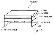
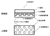
- An optical element includes a metal layer, a dielectric layer laminated on the metal layer, and a phosphor layer that is laminated on the dielectric layer and emits fluorescence by incident light.
- a diffraction grating is formed at the interface between the layer and the phosphor layer, and the dielectric constant of the dielectric layer is higher than 2.25.
- each layer is very thin and the difference in thickness between the layers is large, so that it is difficult to illustrate each layer with an accurate scale and ratio.
- the layers are not schematically drawn but are shown schematically.
- a plane parallel to the substrate 11 is defined as an XY plane, and a direction orthogonal to the XY plane is defined as a Z direction.
- Re [] represents taking a real part in [].
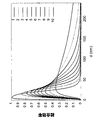
- the interaction distance which is the distance from the exciton to the metal layer 12
- the coupling efficiency between the exciton and the surface plasmon becomes smaller.
- the distance from the surface of the phosphor layer 14 opposite to the high dielectric constant layer 13 to the metal layer 12 is an effective interaction distance that is an interaction distance at which the surface plasmon intensity is e-2 times the maximum value. You can do it.
- the effective interaction distance deff is an effective interaction distance that is an interaction distance at which the surface plasmon intensity is e-2 times the maximum value. You can do it.
- the effective interaction distance deff is
- the dielectric constant of the metal layer 12 since the dielectric constant of the metal layer 12 has an imaginary part, the surface plasmon is excited even if the real part of the effective dielectric constant of the input / output part exceeds the absolute value of the real part of the dielectric constant of the metal layer 12. However, if the difference between the absolute values of the real part of the effective dielectric constant of the incident / exit part and the real part of the dielectric constant of the metal layer 12 is large, the surface plasmon is not excited.
- 4 to 9 are diagrams showing an example of the phosphor layer 14, and shows a cross section of the optical element 1 cut along the YZ plane and an upper surface of the optical element 1 viewed from the + Z direction.
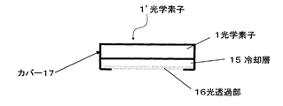
- FIG. 10 is a diagram showing another form of the optical element. 10, in addition to the optical element 1 shown in FIG. 1, the optical element 1 ′ includes a cooling layer 15 provided on the phosphor layer 14, and a cover 17 that covers the optical element 1 and the cooling layer 15. Also have.
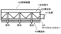
- FIG. 11 is a diagram showing the lighting device 40.
- the illumination device 40 includes the optical element 1, a light source 41, a light guide 42 on which light from the light source is incident, and a dichroic mirror 43.
- the light sources 101A to 101C emit light having a wavelength capable of generating fluorescence in each of the optical elements 1A to 1C.
- each of the dichroic mirrors 102A to 102C transmits the light of each of the light sources 101A to 101C and enters each of the optical elements 1A to 1C. Further, each of the dichroic mirrors 102A to 102C reflects the fluorescence emitted from the respective phosphor layers 14 of the optical elements 1A to 1C, and enters each of the display elements 103A to 103C.
- FIG. 17 is a diagram showing another example of a projector using an optical element.
- the color synthesis prism 203 synthesizes the fluorescence from each of the display elements 202A to 202C and emits it through the projection lens 204.
- the dichroic mirror 305 transmits blue light and red light and reflects green light. More specifically, the dichroic mirror 305 transmits the blue light from the light source 301 ⁇ / b> A and enters the color wheel 302 via the condenser lens 304. Further, the dichroic mirror 305 transmits red light from the light source 301 ⁇ / b> B and enters the display element 307 through the condenser lens 306. The dichroic mirror 305 reflects the green light from the color wheel 302 and enters the display element 307 via the condenser lens 306.
Landscapes
- Physics & Mathematics (AREA)
- General Physics & Mathematics (AREA)
- Optics & Photonics (AREA)
- Engineering & Computer Science (AREA)
- Multimedia (AREA)
- Astronomy & Astrophysics (AREA)
- Spectroscopy & Molecular Physics (AREA)
- Signal Processing (AREA)
- Optical Filters (AREA)
- Non-Portable Lighting Devices Or Systems Thereof (AREA)
- Planar Illumination Modules (AREA)
- Projection Apparatus (AREA)
Abstract
L'invention concerne un élément optique permettant d'augmenter la résistance optique d'une lumière fluorescente émise par un corps fluorescent tout en améliorant les capacités directionnelles de la lumière fluorescente. Un élément optique (1) comprend une couche métallique (12), une couche fortement diélectrique (13) stratifiée sur la couche métallique (12), et une couche de corps fluorescent (14) afin d'émettre de la lumière fluorescente à partir de la lumière incidente, stratifiée sur la couche fortement diélectrique (13). En outre, une structure de réseau (21) fonctionnant comme un réseau de diffraction est disposée au niveau de l'interface entre la couche fortement diélectrique (13) et la couche de corps fluorescent (14). La constante diélectrique de la couche fortement diélectrique (13) est supérieure à 2,25.
Priority Applications (1)
| Application Number | Priority Date | Filing Date | Title |
|---|---|---|---|
| JP2013508801A JPWO2012137583A1 (ja) | 2011-04-07 | 2012-03-15 | 光学素子、カラーホイール、照明装置および投射型表示装置 |
Applications Claiming Priority (4)
| Application Number | Priority Date | Filing Date | Title |
|---|---|---|---|
| JP2011-085364 | 2011-04-07 | ||
| JP2011085364 | 2011-04-07 | ||
| JP2012001320 | 2012-01-06 | ||
| JP2012-001320 | 2012-01-06 |
Publications (1)
| Publication Number | Publication Date |
|---|---|
| WO2012137583A1 true WO2012137583A1 (fr) | 2012-10-11 |
Family
ID=46968987
Family Applications (1)
| Application Number | Title | Priority Date | Filing Date |
|---|---|---|---|
| PCT/JP2012/056729 Ceased WO2012137583A1 (fr) | 2011-04-07 | 2012-03-15 | Élément optique, roue en couleur, dispositif d'éclairage et dispositif d'affichage par projection |
Country Status (2)
| Country | Link |
|---|---|
| JP (1) | JPWO2012137583A1 (fr) |
| WO (1) | WO2012137583A1 (fr) |
Cited By (12)
| Publication number | Priority date | Publication date | Assignee | Title |
|---|---|---|---|---|
| JP2016099520A (ja) * | 2014-11-21 | 2016-05-30 | 日亜化学工業株式会社 | 波長変換部材および該波長変換部材を備えたプロジェクタ |
| JP2016170382A (ja) * | 2015-03-13 | 2016-09-23 | パナソニックIpマネジメント株式会社 | 表示装置および発光装置 |
| JP2016218367A (ja) * | 2015-05-25 | 2016-12-22 | スタンレー電気株式会社 | 波長変換部材及びそれを用いた照明装置 |
| WO2016208644A1 (fr) * | 2015-06-24 | 2016-12-29 | コニカミノルタ株式会社 | Dispositif optique, dispositif de source lumineuse et dispositif de projection |
| WO2016208645A1 (fr) * | 2015-06-25 | 2016-12-29 | コニカミノルタ株式会社 | Dispositif optique, dispositif de source de lumière et dispositif de projection |
| JP2017040905A (ja) * | 2015-08-20 | 2017-02-23 | パナソニックIpマネジメント株式会社 | 発光装置 |
| WO2017038000A1 (fr) * | 2015-08-28 | 2017-03-09 | パナソニックIpマネジメント株式会社 | Appareil et système d'éclairage |
| JP2018511080A (ja) * | 2015-03-13 | 2018-04-19 | ダウ グローバル テクノロジーズ エルエルシー | ナノ構造材料の方法及び素子 |
| TWI634380B (zh) * | 2015-12-31 | 2018-09-01 | 深圳市光峰光電技術有限公司 | 色輪模組與光源模組 |
| US10359155B2 (en) | 2015-08-20 | 2019-07-23 | Panasonic Intellectual Property Management Co., Ltd. | Light-emitting apparatus |
| WO2019171775A1 (fr) * | 2018-03-06 | 2019-09-12 | ソニー株式会社 | Élément électroluminescent, dispositif de source de lumière et projecteur |
| USRE49093E1 (en) | 2015-03-13 | 2022-06-07 | Panasonic Intellectual Property Management Co., Ltd. | Light-emitting apparatus including photoluminescent layer |
Citations (6)
| Publication number | Priority date | Publication date | Assignee | Title |
|---|---|---|---|---|
| JP2007240361A (ja) * | 2006-03-09 | 2007-09-20 | Sekisui Chem Co Ltd | 局在プラズモン増強センサ |
| JP2009239217A (ja) * | 2008-03-28 | 2009-10-15 | Nikon Corp | 発光ダイオード素子 |
| JP2011013315A (ja) * | 2009-06-30 | 2011-01-20 | Casio Computer Co Ltd | 蛍光体基板及び光源装置、プロジェクタ |
| WO2011040528A1 (fr) * | 2009-09-30 | 2011-04-07 | 日本電気株式会社 | Élément optique, dispositif de source lumineuse et dispositif d'affichage par projection |
| WO2011108138A1 (fr) * | 2010-03-04 | 2011-09-09 | 日本電気株式会社 | Élément optique, appareil de source de lumière et appareil d'affichage du type à projection |
| WO2012049905A1 (fr) * | 2010-10-15 | 2012-04-19 | 日本電気株式会社 | Dispositif optique, source de lumière et dispositif d'affichage à projection |
-
2012
- 2012-03-15 WO PCT/JP2012/056729 patent/WO2012137583A1/fr not_active Ceased
- 2012-03-15 JP JP2013508801A patent/JPWO2012137583A1/ja active Pending
Patent Citations (6)
| Publication number | Priority date | Publication date | Assignee | Title |
|---|---|---|---|---|
| JP2007240361A (ja) * | 2006-03-09 | 2007-09-20 | Sekisui Chem Co Ltd | 局在プラズモン増強センサ |
| JP2009239217A (ja) * | 2008-03-28 | 2009-10-15 | Nikon Corp | 発光ダイオード素子 |
| JP2011013315A (ja) * | 2009-06-30 | 2011-01-20 | Casio Computer Co Ltd | 蛍光体基板及び光源装置、プロジェクタ |
| WO2011040528A1 (fr) * | 2009-09-30 | 2011-04-07 | 日本電気株式会社 | Élément optique, dispositif de source lumineuse et dispositif d'affichage par projection |
| WO2011108138A1 (fr) * | 2010-03-04 | 2011-09-09 | 日本電気株式会社 | Élément optique, appareil de source de lumière et appareil d'affichage du type à projection |
| WO2012049905A1 (fr) * | 2010-10-15 | 2012-04-19 | 日本電気株式会社 | Dispositif optique, source de lumière et dispositif d'affichage à projection |
Cited By (21)
| Publication number | Priority date | Publication date | Assignee | Title |
|---|---|---|---|---|
| JP2016099520A (ja) * | 2014-11-21 | 2016-05-30 | 日亜化学工業株式会社 | 波長変換部材および該波長変換部材を備えたプロジェクタ |
| JP2016170382A (ja) * | 2015-03-13 | 2016-09-23 | パナソニックIpマネジメント株式会社 | 表示装置および発光装置 |
| CN105974722A (zh) * | 2015-03-13 | 2016-09-28 | 松下知识产权经营株式会社 | 显示装置以及发光装置 |
| USRE49093E1 (en) | 2015-03-13 | 2022-06-07 | Panasonic Intellectual Property Management Co., Ltd. | Light-emitting apparatus including photoluminescent layer |
| CN105974722B (zh) * | 2015-03-13 | 2020-08-11 | 松下知识产权经营株式会社 | 显示装置以及发光装置 |
| JP2018511080A (ja) * | 2015-03-13 | 2018-04-19 | ダウ グローバル テクノロジーズ エルエルシー | ナノ構造材料の方法及び素子 |
| JP2016218367A (ja) * | 2015-05-25 | 2016-12-22 | スタンレー電気株式会社 | 波長変換部材及びそれを用いた照明装置 |
| WO2016208644A1 (fr) * | 2015-06-24 | 2016-12-29 | コニカミノルタ株式会社 | Dispositif optique, dispositif de source lumineuse et dispositif de projection |
| WO2016208645A1 (fr) * | 2015-06-25 | 2016-12-29 | コニカミノルタ株式会社 | Dispositif optique, dispositif de source de lumière et dispositif de projection |
| US10359155B2 (en) | 2015-08-20 | 2019-07-23 | Panasonic Intellectual Property Management Co., Ltd. | Light-emitting apparatus |
| JP2017040905A (ja) * | 2015-08-20 | 2017-02-23 | パナソニックIpマネジメント株式会社 | 発光装置 |
| USRE50041E1 (en) | 2015-08-20 | 2024-07-16 | Panasonic Intellectual Property Management Co., Ltd. | Light-emitting apparatus |
| WO2017038000A1 (fr) * | 2015-08-28 | 2017-03-09 | パナソニックIpマネジメント株式会社 | Appareil et système d'éclairage |
| TWI634380B (zh) * | 2015-12-31 | 2018-09-01 | 深圳市光峰光電技術有限公司 | 色輪模組與光源模組 |
| WO2019171775A1 (fr) * | 2018-03-06 | 2019-09-12 | ソニー株式会社 | Élément électroluminescent, dispositif de source de lumière et projecteur |
| CN111788521A (zh) * | 2018-03-06 | 2020-10-16 | 索尼公司 | 发光元件、光源装置以及投影仪 |
| KR20200130258A (ko) * | 2018-03-06 | 2020-11-18 | 소니 주식회사 | 발광 소자, 광원 장치 및 프로젝터 |
| JPWO2019171775A1 (ja) * | 2018-03-06 | 2021-03-18 | ソニー株式会社 | 発光素子、光源装置及びプロジェクタ |
| US11429015B2 (en) | 2018-03-06 | 2022-08-30 | Sony Corporation | Light-emitting element, light source device and projector |
| JP2023088975A (ja) * | 2018-03-06 | 2023-06-27 | ソニーグループ株式会社 | 発光素子、光源装置及びプロジェクタ |
| KR102694227B1 (ko) * | 2018-03-06 | 2024-08-09 | 소니그룹주식회사 | 발광 소자, 광원 장치 및 프로젝터 |
Also Published As
| Publication number | Publication date |
|---|---|
| JPWO2012137583A1 (ja) | 2014-07-28 |
Similar Documents
| Publication | Publication Date | Title |
|---|---|---|
| WO2012137583A1 (fr) | Élément optique, roue en couleur, dispositif d'éclairage et dispositif d'affichage par projection | |
| WO2012137584A1 (fr) | Élément optique, dispositif d'éclairage et dispositif d'affichage par projection | |
| JP5664657B2 (ja) | 光学素子、光源および投射型表示装置 | |
| CN102341740B (zh) | 发光单元阵列、其制造方法和投影设备 | |
| EP3229072B1 (fr) | Système d'éclairage et appareil de projection | |
| CN107250909B (zh) | 照明装置和图像投影设备 | |
| US20170133357A1 (en) | Display device | |
| JP2023067957A (ja) | 発光装置、表示装置および照明装置 | |
| JP2016171228A (ja) | 発光素子、発光装置および検知装置 | |
| JP5776689B2 (ja) | 表示素子、表示器及び投射型表示装置 | |
| JPWO2013046866A1 (ja) | 光素子および該光素子を用いた投射型表示装置 | |
| JPWO2013103037A1 (ja) | 光学装置、光学素子および画像表示装置 | |
| JP2017157488A (ja) | 光学装置、光源装置及び投影装置 | |
| CN111788521B (zh) | 发光元件、光源装置以及投影仪 | |
| CN105974722B (zh) | 显示装置以及发光装置 | |
| WO2016208644A1 (fr) | Dispositif optique, dispositif de source lumineuse et dispositif de projection | |
| US20150109587A1 (en) | Optical element, lighting device, and image display device | |
| JPWO2013046872A1 (ja) | 光学素子、光源装置及び投射型表示装置 | |
| JP2006083260A (ja) | 蛍光体粒子、蛍光体粒子分散体ならびにこれらを含む照明装置および表示装置。 | |
| JP2019159032A (ja) | 光源装置およびプロジェクター | |
| US8723208B2 (en) | Light-emitting device having a fine structure interposed between a light-emitting layer and a substrate | |
| TWM545921U (zh) | 光源結構及其背光模組 | |
| JPWO2013103038A1 (ja) | 光学装置および画像表示装置 | |
| WO2016208645A1 (fr) | Dispositif optique, dispositif de source de lumière et dispositif de projection |
Legal Events
| Date | Code | Title | Description |
|---|---|---|---|
| 121 | Ep: the epo has been informed by wipo that ep was designated in this application |
Ref document number: 12767564 Country of ref document: EP Kind code of ref document: A1 |
|
| ENP | Entry into the national phase |
Ref document number: 2013508801 Country of ref document: JP Kind code of ref document: A |
|
| NENP | Non-entry into the national phase |
Ref country code: DE |
|
| 122 | Ep: pct application non-entry in european phase |
Ref document number: 12767564 Country of ref document: EP Kind code of ref document: A1 |