WO2012137584A1 - Élément optique, dispositif d'éclairage et dispositif d'affichage par projection - Google Patents
Élément optique, dispositif d'éclairage et dispositif d'affichage par projection Download PDFInfo
- Publication number
- WO2012137584A1 WO2012137584A1 PCT/JP2012/056730 JP2012056730W WO2012137584A1 WO 2012137584 A1 WO2012137584 A1 WO 2012137584A1 JP 2012056730 W JP2012056730 W JP 2012056730W WO 2012137584 A1 WO2012137584 A1 WO 2012137584A1
- Authority
- WO
- WIPO (PCT)
- Prior art keywords
- optical element
- light
- light guide
- guide plate
- phosphor layer
- Prior art date
- Legal status (The legal status is an assumption and is not a legal conclusion. Google has not performed a legal analysis and makes no representation as to the accuracy of the status listed.)
- Ceased
Links
Images


Classifications
-
- G—PHYSICS
- G02—OPTICS
- G02B—OPTICAL ELEMENTS, SYSTEMS OR APPARATUS
- G02B6/00—Light guides; Structural details of arrangements comprising light guides and other optical elements, e.g. couplings
- G02B6/0001—Light guides; Structural details of arrangements comprising light guides and other optical elements, e.g. couplings specially adapted for lighting devices or systems
- G02B6/0011—Light guides; Structural details of arrangements comprising light guides and other optical elements, e.g. couplings specially adapted for lighting devices or systems the light guides being planar or of plate-like form
- G02B6/0013—Means for improving the coupling-in of light from the light source into the light guide
- G02B6/0015—Means for improving the coupling-in of light from the light source into the light guide provided on the surface of the light guide or in the bulk of it
- G02B6/0016—Grooves, prisms, gratings, scattering particles or rough surfaces
-
- G—PHYSICS
- G03—PHOTOGRAPHY; CINEMATOGRAPHY; ANALOGOUS TECHNIQUES USING WAVES OTHER THAN OPTICAL WAVES; ELECTROGRAPHY; HOLOGRAPHY
- G03B—APPARATUS OR ARRANGEMENTS FOR TAKING PHOTOGRAPHS OR FOR PROJECTING OR VIEWING THEM; APPARATUS OR ARRANGEMENTS EMPLOYING ANALOGOUS TECHNIQUES USING WAVES OTHER THAN OPTICAL WAVES; ACCESSORIES THEREFOR
- G03B21/00—Projectors or projection-type viewers; Accessories therefor
- G03B21/14—Details
- G03B21/20—Lamp housings
- G03B21/2006—Lamp housings characterised by the light source
- G03B21/2033—LED or laser light sources
- G03B21/204—LED or laser light sources using secondary light emission, e.g. luminescence or fluorescence
-
- H—ELECTRICITY
- H04—ELECTRIC COMMUNICATION TECHNIQUE
- H04N—PICTORIAL COMMUNICATION, e.g. TELEVISION
- H04N9/00—Details of colour television systems
- H04N9/12—Picture reproducers
- H04N9/31—Projection devices for colour picture display, e.g. using electronic spatial light modulators [ESLM]
- H04N9/3141—Constructional details thereof
- H04N9/315—Modulator illumination systems
Definitions
- the present invention relates to an optical element, an illumination device, and a projection display device.
- Such a projector includes an LED, an illumination optical system into which light from the LED is incident, a modulation element that modulates and emits light from the illumination optical system in accordance with a video signal, and light from the modulation element on a screen. And a projection optical system for projecting onto the screen.
- LEDs Light Emitting Diodes
- an illumination optical system there is an illumination optical system in which light emitted from an LED is incident on a phosphor and fluorescence generated by the phosphor is incident on a modulation element.
- a projector using such an illumination optical system it is desired to increase the light intensity of fluorescence in order to increase the brightness of the projected image.
- Non-Patent Document 1 There is an optical element described in Non-Patent Document 1 as a technique for increasing the light intensity of fluorescence.
- a metal thin film and a dielectric layer having a grating structure are laminated on a substrate in this order.
- the dielectric layer is coated with quantum dots that function as phosphors.
- Non-Patent Document 1 in addition to photons extracted when there is no grating structure, photons extracted by diffraction of surface plasmons are added, so that the light intensity of fluorescence can be enhanced. For this reason, if the optical element described in Non-Patent Document 1 is applied to a fluorescent illumination device that performs illumination with fluorescence, the luminance of the fluorescent illumination device can be improved.
- Non-Patent Document 1 When the optical element described in Non-Patent Document 1 is used for the illumination optical system of the projector, in addition to the optical element, light from the LED is incident on the optical element, or fluorescence generated by the optical element is incident on the modulation element. Therefore, an optical system such as a condensing lens is required, which causes a problem of increasing the size of the projector.
- An object of the present invention is to provide an optical element capable of suppressing an increase in size while increasing the light intensity of fluorescence.
- An optical element includes a light guide plate that propagates light incident from a light source, a phosphor layer that is provided on the light guide plate and generates fluorescence by light from the light guide plate, and is laminated on the phosphor layer. And a diffraction grating is formed at the interface between the light guide plate and the phosphor layer.
- the lighting device of the present invention includes the above-described optical element and a light source that makes light incident on a light guide plate of the optical element.
- the projection type image display device of the present invention has the illumination device described above.
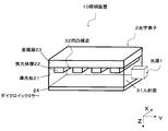
- FIG. 1 is a perspective view schematically showing a lighting device according to a first embodiment of the present invention. Note that in an actual lighting device, the thickness of each layer is very thin and the difference in thickness between the layers is large, so that it is difficult to illustrate each layer with an accurate scale and ratio. For this reason, in the drawings, the layers are not schematically drawn but are shown schematically.
- the 1 includes a light source 1 that emits light and an optical element 2 on which the light emitted from the light source 1 is incident.
- the light source 1 is, for example, an LED, and is disposed on the outer periphery of the optical element 2.
- the light source 1 is disposed so as to contact the optical element 2, but may be disposed at a position away from the optical element 2, for example, optically via a light guide member such as a light pipe.
- the optical element 2 may be connected.
- the optical element 2 includes a light guide plate 21, a phosphor layer 22, a metal layer 23, and a dichroic mirror 24.
- the light guide plate 21 receives light emitted from the light source 1 and propagates the incident light inside.
- the light guide plate 21 is formed in a flat plate shape, and is provided so that the light source 1 contacts the side surface.
- the side surface in contact with the light source 1 is referred to as an incident surface 31.
- the shape of the light guide plate 21 is not limited to a flat plate shape.
- the upper surface of the light guide plate 21 is the XY plane, and the direction orthogonal to the XY plane is the Z direction.
- a phosphor layer 22 is provided on the upper surface of the light guide plate 21.
- the light guide plate 21 is provided with an uneven structure 32 that functions as a diffraction grating at the interface with the phosphor layer 22.
- the unevenness of the uneven structure 32 is arranged in a one-dimensional lattice shape, but other arrangements such as a triangular lattice shape may be used.
- the phosphor layer 22 is provided on the upper surface of the light guide plate 21.
- the phosphor layer 22 is a carrier generation layer that absorbs incident light incident from the light guide plate 21 to generate excitons (carriers) and generates fluorescence by the excitons.
- the material of the phosphor layer 22 is preferably a nano inorganic phosphor such as a quantum dot phosphor, but may be an inorganic phosphor such as Eu, BaMgAlxOy: Eu, BaMgAlxOy: Mn, or an organic phosphor.
- the light guide plate 21 has an uneven structure 32 that functions as a diffraction grating (grating) at the interface with the phosphor layer 22.
- the concavo-convex structure 32 the concavo-convex portions are arranged in a one-dimensional lattice pattern. Note that the unevenness of the uneven structure may be arranged like a triangular lattice.
- the metal layer 23 is laminated on the phosphor layer 22.
- the material of the metal layer 23 include gold, silver, copper, platinum, palladium, rhodium, osmium, ruthenium, iridium, iron, tin, zinc, cobalt, nickel, chromium, titanium, tantalum, tungsten, indium, aluminum, Alternatively, they are made of these alloys.
- the thickness of the metal layer 23 is preferably 200 nm or less, particularly preferably about 10 nm to 100 nm.
- the dichroic mirror 24 is a wavelength selective member provided on the surface opposite to the surface on which the phosphor layer 22 of the light guide plate 21 is provided.
- the dichroic mirror 24 reflects the light emitted from the light source 1, transmits the fluorescence generated in the phosphor layer 22, and emits only the fluorescence from the optical element 2.
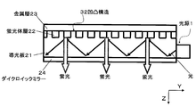
- FIG. 2 is a view for explaining the behavior of light in the illumination device 10, and shows a longitudinal section of the illumination device 10 shown in FIG. 1 cut along a YZ plane.
- the light when light is emitted from the light source 1, the light enters the incident surface 31 of the light guide plate 21.
- the light incident on the incident surface 31 is reflected by the dichroic mirror 24 and enters the phosphor layer 22.
- a configuration in which light incident on the incident surface 31 is directly incident on the phosphor layer 22 may be employed.
- Part of the light incident on the phosphor layer 22 is reflected by the phosphor layer 22 and returned to the light guide plate 21.
- the light returned to the light guide plate 21 is reflected by the dichroic mirror 24 and reenters the phosphor layer 22.
- the remainder of the light incident on the phosphor layer 22 is absorbed by the phosphor layer 22 and excitons are excited in the phosphor layer 22.
- a part of the excitons is converted into fluorescence by being relaxed and emitted from the optical element 2.
- the remaining part of the excitons excites surface plasmons at the interface between the metal layer 23 and the phosphor layer 22.
- the excited surface plasmon is diffracted by the concavo-convex structure 32 and emitted from the optical element 2.
- the wave number k spp is determined according to the dielectric constant distribution of the incident / exit portion of the optical element 2.
- the entrance / exit portion is a dielectric constant distribution of a medium (in FIG. 1, the light guide plate 21 and the phosphor layer 22) closer to the light guide plate 21 than the metal layer 23.
- ⁇ eff is an effective dielectric constant of the incident / exit portion.
- the effective dielectric constant ⁇ eff is the incident / exit portion when the angular frequency of the fluorescence emitted from the phosphor layer 22 is ⁇ , the permittivity distribution of the incident / exit portion is ⁇ ( ⁇ , x, y, z), and the imaginary unit is j.
- ⁇ eff is an effective dielectric constant of the incident / exit portion.
- the effective dielectric constant ⁇ eff is the incident / exit portion when the angular frequency of the fluorescence emitted from the phosphor layer 22 is ⁇
- the permittivity distribution of the incident / exit portion is ⁇ ( ⁇ , x, y, z)
- the imaginary unit is j.
- Re [] represents taking a real part in [].
- the effective dielectric constant ⁇ eff may be calculated using the following equation. However, it is particularly desirable to use equation (3).
- the wave number k spp can be obtained from the permittivity distribution ⁇ ( ⁇ , x, y, z) of the incident / exit portion. More specifically, the permittivity distribution ⁇ ( ⁇ , x, y, z) of the input / output portion is substituted into the equation (3), and an appropriate initial value is given to the effective permittivity ⁇ eff .
- the actual effective dielectric constant ⁇ eff is calculated by repeatedly calculating the surface plasmon wavenumbers k spp and k spp, Z and the effective dielectric constant ⁇ eff using the equations (2) and (3).
- the wave number k spp can be obtained from the actual effective dielectric constant ⁇ eff .
- FIG. 3 is a graph showing the relationship between the coupling efficiency between excitons and surface plasmons, the interaction distance from the excitons to the metal layer 23, and the dielectric constant of the light guide plate 21.
- the coupling efficiency between excitons and surface plasmons indicates the ratio of excitons that excite surface plasmons among the excited excitons.
- the distance from the surface of the phosphor layer 22 opposite to the metal layer 23 to the metal layer 23 is set to an effective interaction distance that is an interaction distance at which the surface plasmon intensity is e ⁇ 2 times the maximum value. That's fine.
- the effective interaction distance d eff is an effective interaction distance at which the surface plasmon intensity is e ⁇ 2 times the maximum value. That's fine.
- the effective interaction distance d eff in an actual optical element is on the order of several hundred nanometers, in order to increase the coupling efficiency of fluorescence and surface plasmon, particles of the fluorescent material that is the material of the phosphor layer 22 are used.
- the diameter is preferably in the nanometer order.
- the maximum value of the coupling efficiency between excitons and surface plasmons increases as the dielectric constant of the light guide plate 21 increases. For this reason, it is desirable that the dielectric constant of the light guide plate 21 is higher.
- the real part of the effective dielectric constant of the incident / exit part exceeds the absolute value of the real part of the dielectric constant of the metal layer 23, the surface plasmon is not excited as shown in the equation (2).
- the dielectric constant of the metal layer 12 has an imaginary part, even if the real part of the effective dielectric constant of the input / output part exceeds the absolute value of the real part of the dielectric constant of the metal layer 23, the surface plasmon is excited. However, if the difference between the absolute value of the real part of the effective dielectric constant of the incident / exit part and the real part of the dielectric constant of the metal layer 23 is large, the surface plasmon is not excited.
- the optical element 2 includes the phosphor layer 22 provided on the light guide plate 21 and the metal layer 23 laminated on the phosphor layer 22, and the light guide plate 21 and the phosphor.
- a diffraction grating is formed at the interface of the layer 22. Since excitons in the phosphor layer 22 excite surface plasmons at the interface between the phosphor layer 22 and the metal layer 23 and the surface plasmons can be extracted as fluorescence, the light intensity of the fluorescence can be increased. It becomes possible. Further, since the fluorescence emitted from the light guide plate 21 can be incident on the display element, the optical element 2 can be used as the illumination optical system of the projector, and the optical element 2 and the illumination optical system are integrally formed. Therefore, it is possible to suppress an increase in the size of the optical element.
- the size of the exit surface of the optical element 2 can be made relatively small.
- the optical element 2 can be easily manufactured. It becomes possible to do. Further, since the phosphor layer 22 can be produced by a screen printing process, the optical element 2 can be produced more easily.
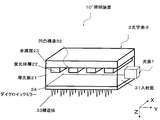
- FIG. 4 is a perspective view schematically showing a lighting device according to a second embodiment of the present invention.
- FIG. 5 is a diagram for explaining the behavior of light in the illumination device according to the second embodiment of the present invention, and shows a longitudinal section obtained by cutting the illumination device shown in FIG. 4 along the YZ plane. .
- FIG. 4 and FIG. 5 further includes a structure 33 in addition to the configuration shown in FIG.
- the structure 33 is provided on the surface opposite to the surface on which the light guide plate 21 of the dichroic mirror 24 is provided.
- the structure 33 suppresses reflection of fluorescence emitted from the phosphor layer 22 and improves the transmittance of fluorescence in the dichroic mirror 24.
- Examples of the structure 33 include a photonic crystal, a moth-eye structure, and a lens array.
- the fluorescence transmittance is improved by the structure 33, it is possible to improve the luminance of the fluorescence emitted from the illumination device 10 '.
- FIG. 6 is a perspective view showing an illumination apparatus according to a third embodiment of the present invention.
- the illumination device 10 ′′ shown in FIG. 6 is different from the illumination device 10 shown in FIG. 1 in that the phosphor layer 22 has metal fine particles 34.
- the metal fine particles 34 increase the apparent absorbance of incident light incident on the phosphor layer 22.
- the apparent absorbance is the absorbance when the phosphor layer 22 is regarded as a homogeneous layer and light is incident on the entire surface of the phosphor layer 22.
- the metal fine particles 34 interact with the incident light to excite surface plasmons on the surface of the metal fine particles 34 and induce an enhanced electric field in the vicinity of the surface that is nearly 100 times larger than the electric field intensity of the incident light. . Since the excitons are also generated in the phosphor layer 22 by this enhanced electric field, the number of excitons in the phosphor layer 22 increases. For this reason, the metal fine particles 34 can increase the apparent absorbance of the incident light by the surface plasmons excited on the surface of the metal fine particles 34 and increase the light intensity of the fluorescence.
- Examples of the material of the metal fine particles 34 include gold, silver, copper, platinum, palladium, rhodium, osmium, ruthenium, iridium, iron, tin, zinc, cobalt, nickel, chromium, titanium, tantalum, tungsten, indium, aluminum, Or these alloys etc. are mentioned.
- gold, silver, copper, platinum, aluminum, or an alloy containing these as a main component is preferable, and gold, silver, aluminum, or an alloy containing these as a main component is particularly preferable.
- the metal fine particles 34 may have a core-shell structure in which metal species are different in the periphery and the center, a hemispherical union structure in which two hemispheres are combined, or a cluster-in-cluster structure in which different clusters gather to form fine particles.
- the resonance wavelength can be controlled without changing the size or shape of the fine particles.
- the shape of the metal fine particles 34 may be any shape as long as it has a closed surface, such as a rectangular parallelepiped, a cube, an ellipsoid, a sphere, a triangular pyramid, and a triangular prism. Further, the metal fine particles 34 include those obtained by processing a metal thin film into a structure constituted by a closed surface having a side of less than 10 ⁇ m by fine processing typified by semiconductor lithography technology.
- the light intensity of the fluorescence can be increased by the metal fine particles 34 in the phosphor layer 22, so that the luminance can be improved.
- FIG. 7 is a diagram showing a configuration of a projector using the illumination device.
- the projector shown in FIG. 7 includes illumination devices 101A to 101C, display elements 102A to 102C, a color synthesis prism 103, and a projection lens 104.
- the illuminating devices 101A to 101C are configured by the illuminating device 10 shown in FIG. 1, the illuminating device 10 ′ shown in FIG. 2, or the illuminating device 10 ′′ shown in FIG.
- the body layer 22 generates fluorescence of different colors, for example, the phosphor layer 22 in each of the lighting devices 101A to 101C generates red, green, and blue fluorescence.
- Each of the display elements 102A to 102C modulates the fluorescence from each of the illumination devices 101A to 101C in accordance with the video signal and outputs the modulated fluorescence to the color synthesis prism 103.
- each of the display elements 102A to 102C is arranged so as to come into contact with the dichroic mirror 24 of each of the lighting devices 101A to 101C, but may be arranged at a position away from the dichroic mirror 24. .
- the color synthesizing prism 103 synthesizes the fluorescence from each of the display elements 102A to 102C and emits it through the projection lens 104.
Landscapes
- Physics & Mathematics (AREA)
- Engineering & Computer Science (AREA)
- Multimedia (AREA)
- Optics & Photonics (AREA)
- General Physics & Mathematics (AREA)
- Signal Processing (AREA)
- Projection Apparatus (AREA)
- Non-Portable Lighting Devices Or Systems Thereof (AREA)
- Planar Illumination Modules (AREA)
Abstract
Priority Applications (2)
| Application Number | Priority Date | Filing Date | Title |
|---|---|---|---|
| US14/110,296 US20140022818A1 (en) | 2011-04-07 | 2012-03-15 | Optical element, illumination device, and projection display device |
| JP2013508802A JPWO2012137584A1 (ja) | 2011-04-07 | 2012-03-15 | 光学素子、照明装置および投射型表示装置 |
Applications Claiming Priority (4)
| Application Number | Priority Date | Filing Date | Title |
|---|---|---|---|
| JP2011085370 | 2011-04-07 | ||
| JP2011-085370 | 2011-04-07 | ||
| JP2012-001321 | 2012-01-06 | ||
| JP2012001321 | 2012-01-06 |
Publications (1)
| Publication Number | Publication Date |
|---|---|
| WO2012137584A1 true WO2012137584A1 (fr) | 2012-10-11 |
Family
ID=46968988
Family Applications (1)
| Application Number | Title | Priority Date | Filing Date |
|---|---|---|---|
| PCT/JP2012/056730 Ceased WO2012137584A1 (fr) | 2011-04-07 | 2012-03-15 | Élément optique, dispositif d'éclairage et dispositif d'affichage par projection |
Country Status (3)
| Country | Link |
|---|---|
| US (1) | US20140022818A1 (fr) |
| JP (1) | JPWO2012137584A1 (fr) |
| WO (1) | WO2012137584A1 (fr) |
Cited By (18)
| Publication number | Priority date | Publication date | Assignee | Title |
|---|---|---|---|---|
| JP2014235891A (ja) * | 2013-06-03 | 2014-12-15 | Nsマテリアルズ株式会社 | 導光体、バックライトユニット及び導光体の製造方法 |
| US9515239B2 (en) | 2014-02-28 | 2016-12-06 | Panasonic Intellectual Property Management Co., Ltd. | Light-emitting device and light-emitting apparatus |
| US9518215B2 (en) | 2014-02-28 | 2016-12-13 | Panasonic Intellectual Property Management Co., Ltd. | Light-emitting device and light-emitting apparatus |
| US9618697B2 (en) | 2014-02-28 | 2017-04-11 | Panasonic Intellectual Property Management Co., Ltd. | Light directional angle control for light-emitting device and light-emitting apparatus |
| US9880336B2 (en) | 2014-02-28 | 2018-01-30 | Panasonic Intellectual Property Management Co., Ltd. | Light-emitting device including photoluminescent layer |
| US9882100B2 (en) | 2015-08-20 | 2018-01-30 | Panasonic Intellectual Property Management Co., Ltd. | Light-emitting device having surface structure for limiting directional angle of light |
| US9890912B2 (en) | 2014-02-28 | 2018-02-13 | Panasonic Intellectual Property Management Co., Ltd. | Light-emitting apparatus including photoluminescent layer |
| US9899577B2 (en) | 2015-06-08 | 2018-02-20 | Panasonic Intellectual Property Management Co., Ltd. | Light-emitting apparatus including photoluminescent layer |
| US10012780B2 (en) | 2014-02-28 | 2018-07-03 | Panasonic Intellectual Property Management Co., Ltd. | Light-emitting device including photoluminescent layer |
| US10031276B2 (en) | 2015-03-13 | 2018-07-24 | Panasonic Intellectual Property Management Co., Ltd. | Display apparatus including photoluminescent layer |
| US10094522B2 (en) | 2016-03-30 | 2018-10-09 | Panasonic Intellectual Property Management Co., Ltd. | Light-emitting device having photoluminescent layer |
| US10115874B2 (en) | 2015-06-08 | 2018-10-30 | Panasonic Intellectual Property Management Co., Ltd. | Light-emitting device including photoluminescent layer |
| US10113712B2 (en) | 2015-03-13 | 2018-10-30 | Panasonic Intellectual Property Management Co., Ltd. | Light-emitting device including photoluminescent layer |
| US10182702B2 (en) | 2015-03-13 | 2019-01-22 | Panasonic Intellectual Property Management Co., Ltd. | Light-emitting apparatus including photoluminescent layer |
| US10359155B2 (en) | 2015-08-20 | 2019-07-23 | Panasonic Intellectual Property Management Co., Ltd. | Light-emitting apparatus |
| JP2021047374A (ja) * | 2019-09-20 | 2021-03-25 | セイコーエプソン株式会社 | 波長変換素子、光源装置及びプロジェクター |
| USRE49093E1 (en) | 2015-03-13 | 2022-06-07 | Panasonic Intellectual Property Management Co., Ltd. | Light-emitting apparatus including photoluminescent layer |
| USRE50041E1 (en) | 2015-08-20 | 2024-07-16 | Panasonic Intellectual Property Management Co., Ltd. | Light-emitting apparatus |
Families Citing this family (8)
| Publication number | Priority date | Publication date | Assignee | Title |
|---|---|---|---|---|
| JP5776689B2 (ja) * | 2010-05-14 | 2015-09-09 | 日本電気株式会社 | 表示素子、表示器及び投射型表示装置 |
| WO2012049905A1 (fr) * | 2010-10-15 | 2012-04-19 | 日本電気株式会社 | Dispositif optique, source de lumière et dispositif d'affichage à projection |
| US9170351B2 (en) * | 2011-06-17 | 2015-10-27 | Nec Corporation | Optical element, light source apparatus, and projection-type display apparatus |
| WO2014020954A1 (fr) * | 2012-07-31 | 2014-02-06 | 日本電気株式会社 | Élément optique, dispositif d'éclairement, dispositif d'affichage d'image, procédé de mise en œuvre d'élément optique |
| US10096393B2 (en) | 2014-03-31 | 2018-10-09 | Medtronic, Inc. | Nuclear radiation particle power converter |
| US10290757B2 (en) | 2015-09-09 | 2019-05-14 | Medtronic, Inc. | Power source and method of forming same |
| JP2019532481A (ja) * | 2016-09-07 | 2019-11-07 | コーニング インコーポレイテッド | 色変換導光板および色変換導光板を含む装置 |
| KR102664384B1 (ko) * | 2017-01-02 | 2024-05-08 | 삼성전자주식회사 | 지향성 백라이트 유닛 및 이를 포함하는 영상 표시 장치 |
Citations (2)
| Publication number | Priority date | Publication date | Assignee | Title |
|---|---|---|---|---|
| JP2002358812A (ja) * | 2002-02-12 | 2002-12-13 | Nichia Chem Ind Ltd | 窒化ガリウム系化合物半導体を用いた光源 |
| JP2006073202A (ja) * | 2004-08-31 | 2006-03-16 | Nichia Chem Ind Ltd | 発光装置 |
Family Cites Families (7)
| Publication number | Priority date | Publication date | Assignee | Title |
|---|---|---|---|---|
| EP2069838A2 (fr) * | 2006-10-06 | 2009-06-17 | Qualcomm Mems Technologies, Inc. | Dispositif d'éclairage intégrant un coupleur de lumière |
| US20090034230A1 (en) * | 2007-07-31 | 2009-02-05 | Luminus Devices, Inc. | Illumination assembly including wavelength converting material having spatially varying density |
| US8619363B1 (en) * | 2007-11-06 | 2013-12-31 | Fusion Optix, Inc. | Light redirecting element comprising a forward diffracting region and a scattering region |
| US8177406B2 (en) * | 2007-12-19 | 2012-05-15 | Edward Pakhchyan | Display including waveguide, micro-prisms and micro-mirrors |
| US20100027293A1 (en) * | 2008-07-30 | 2010-02-04 | Intematix Corporation | Light Emitting Panel |
| JP5538519B2 (ja) * | 2010-02-25 | 2014-07-02 | シャープ株式会社 | 発光素子、ディスプレイ及び表示装置 |
| KR101636052B1 (ko) * | 2010-04-23 | 2016-07-04 | 삼성전자주식회사 | 컬러 필터 및 이를 채용한 디스플레이 장치 |
-
2012
- 2012-03-15 JP JP2013508802A patent/JPWO2012137584A1/ja active Pending
- 2012-03-15 WO PCT/JP2012/056730 patent/WO2012137584A1/fr not_active Ceased
- 2012-03-15 US US14/110,296 patent/US20140022818A1/en not_active Abandoned
Patent Citations (2)
| Publication number | Priority date | Publication date | Assignee | Title |
|---|---|---|---|---|
| JP2002358812A (ja) * | 2002-02-12 | 2002-12-13 | Nichia Chem Ind Ltd | 窒化ガリウム系化合物半導体を用いた光源 |
| JP2006073202A (ja) * | 2004-08-31 | 2006-03-16 | Nichia Chem Ind Ltd | 発光装置 |
Cited By (19)
| Publication number | Priority date | Publication date | Assignee | Title |
|---|---|---|---|---|
| JP2014235891A (ja) * | 2013-06-03 | 2014-12-15 | Nsマテリアルズ株式会社 | 導光体、バックライトユニット及び導光体の製造方法 |
| US10012780B2 (en) | 2014-02-28 | 2018-07-03 | Panasonic Intellectual Property Management Co., Ltd. | Light-emitting device including photoluminescent layer |
| US9618697B2 (en) | 2014-02-28 | 2017-04-11 | Panasonic Intellectual Property Management Co., Ltd. | Light directional angle control for light-emitting device and light-emitting apparatus |
| US9880336B2 (en) | 2014-02-28 | 2018-01-30 | Panasonic Intellectual Property Management Co., Ltd. | Light-emitting device including photoluminescent layer |
| US9890912B2 (en) | 2014-02-28 | 2018-02-13 | Panasonic Intellectual Property Management Co., Ltd. | Light-emitting apparatus including photoluminescent layer |
| US9515239B2 (en) | 2014-02-28 | 2016-12-06 | Panasonic Intellectual Property Management Co., Ltd. | Light-emitting device and light-emitting apparatus |
| US9518215B2 (en) | 2014-02-28 | 2016-12-13 | Panasonic Intellectual Property Management Co., Ltd. | Light-emitting device and light-emitting apparatus |
| US10113712B2 (en) | 2015-03-13 | 2018-10-30 | Panasonic Intellectual Property Management Co., Ltd. | Light-emitting device including photoluminescent layer |
| USRE49093E1 (en) | 2015-03-13 | 2022-06-07 | Panasonic Intellectual Property Management Co., Ltd. | Light-emitting apparatus including photoluminescent layer |
| US10182702B2 (en) | 2015-03-13 | 2019-01-22 | Panasonic Intellectual Property Management Co., Ltd. | Light-emitting apparatus including photoluminescent layer |
| US10031276B2 (en) | 2015-03-13 | 2018-07-24 | Panasonic Intellectual Property Management Co., Ltd. | Display apparatus including photoluminescent layer |
| US10115874B2 (en) | 2015-06-08 | 2018-10-30 | Panasonic Intellectual Property Management Co., Ltd. | Light-emitting device including photoluminescent layer |
| US9899577B2 (en) | 2015-06-08 | 2018-02-20 | Panasonic Intellectual Property Management Co., Ltd. | Light-emitting apparatus including photoluminescent layer |
| US10359155B2 (en) | 2015-08-20 | 2019-07-23 | Panasonic Intellectual Property Management Co., Ltd. | Light-emitting apparatus |
| US9882100B2 (en) | 2015-08-20 | 2018-01-30 | Panasonic Intellectual Property Management Co., Ltd. | Light-emitting device having surface structure for limiting directional angle of light |
| USRE50041E1 (en) | 2015-08-20 | 2024-07-16 | Panasonic Intellectual Property Management Co., Ltd. | Light-emitting apparatus |
| US10094522B2 (en) | 2016-03-30 | 2018-10-09 | Panasonic Intellectual Property Management Co., Ltd. | Light-emitting device having photoluminescent layer |
| JP2021047374A (ja) * | 2019-09-20 | 2021-03-25 | セイコーエプソン株式会社 | 波長変換素子、光源装置及びプロジェクター |
| JP7283327B2 (ja) | 2019-09-20 | 2023-05-30 | セイコーエプソン株式会社 | 波長変換素子、光源装置及びプロジェクター |
Also Published As
| Publication number | Publication date |
|---|---|
| US20140022818A1 (en) | 2014-01-23 |
| JPWO2012137584A1 (ja) | 2014-07-28 |
Similar Documents
| Publication | Publication Date | Title |
|---|---|---|
| WO2012137584A1 (fr) | Élément optique, dispositif d'éclairage et dispositif d'affichage par projection | |
| JP5664657B2 (ja) | 光学素子、光源および投射型表示装置 | |
| WO2012137583A1 (fr) | Élément optique, roue en couleur, dispositif d'éclairage et dispositif d'affichage par projection | |
| TWI577631B (zh) | 發光裝置以及採用該發光裝置的顯示裝置 | |
| JP2023067957A (ja) | 発光装置、表示装置および照明装置 | |
| JPWO2013046866A1 (ja) | 光素子および該光素子を用いた投射型表示装置 | |
| JP2016171228A (ja) | 発光素子、発光装置および検知装置 | |
| JPWO2013103037A1 (ja) | 光学装置、光学素子および画像表示装置 | |
| TW201608734A (zh) | 發光裝置以及採用該發光裝置的顯示裝置 | |
| WO2018179540A1 (fr) | Élément et dispositif électroluminescents | |
| WO2011142455A1 (fr) | Élément d'affichage, écran, et dispositif d'affichage par projection | |
| JP2017157488A (ja) | 光学装置、光源装置及び投影装置 | |
| US20150153508A1 (en) | Light source device and display device | |
| WO2013103039A1 (fr) | Elément optique, dispositif optique, dispositif d'affichage d'image et procédé d'amélioration du taux d'absorption de lumière excitée | |
| CN111788521A (zh) | 发光元件、光源装置以及投影仪 | |
| JP2016170382A (ja) | 表示装置および発光装置 | |
| JPWO2013046865A1 (ja) | 光学素子、光源装置及び投射型表示装置 | |
| CN106907620A (zh) | 前置光源和包括该前置光源的显示装置 | |
| WO2016208644A1 (fr) | Dispositif optique, dispositif de source lumineuse et dispositif de projection | |
| WO2013175670A1 (fr) | Élément optique, dispositif d'éclairage et dispositif d'affichage d'image | |
| WO2013046872A1 (fr) | Élément optique, dispositif de source de lumière et dispositif d'affichage du type à projection | |
| JPWO2014020954A1 (ja) | 光学素子、照明装置、画像表示装置、光学素子の作動方法 | |
| US8723208B2 (en) | Light-emitting device having a fine structure interposed between a light-emitting layer and a substrate | |
| TWM545921U (zh) | 光源結構及其背光模組 | |
| JPWO2014020955A1 (ja) | 光学素子、照明装置、画像表示装置、光学素子の作動方法 |
Legal Events
| Date | Code | Title | Description |
|---|---|---|---|
| 121 | Ep: the epo has been informed by wipo that ep was designated in this application |
Ref document number: 12768433 Country of ref document: EP Kind code of ref document: A1 |
|
| ENP | Entry into the national phase |
Ref document number: 2013508802 Country of ref document: JP Kind code of ref document: A |
|
| NENP | Non-entry into the national phase |
Ref country code: DE |
|
| WWE | Wipo information: entry into national phase |
Ref document number: 14110296 Country of ref document: US |
|
| 122 | Ep: pct application non-entry in european phase |
Ref document number: 12768433 Country of ref document: EP Kind code of ref document: A1 |