WO2012140958A1 - Procédé de fabrication pour module optique - Google Patents
Procédé de fabrication pour module optique Download PDFInfo
- Publication number
- WO2012140958A1 WO2012140958A1 PCT/JP2012/054623 JP2012054623W WO2012140958A1 WO 2012140958 A1 WO2012140958 A1 WO 2012140958A1 JP 2012054623 W JP2012054623 W JP 2012054623W WO 2012140958 A1 WO2012140958 A1 WO 2012140958A1
- Authority
- WO
- WIPO (PCT)
- Prior art keywords
- optical fiber
- optical module
- fiber
- base
- optical
- Prior art date
- Legal status (The legal status is an assumption and is not a legal conclusion. Google has not performed a legal analysis and makes no representation as to the accuracy of the status listed.)
- Ceased
Links
Images




Classifications
-
- G—PHYSICS
- G02—OPTICS
- G02B—OPTICAL ELEMENTS, SYSTEMS OR APPARATUS
- G02B6/00—Light guides; Structural details of arrangements comprising light guides and other optical elements, e.g. couplings
- G02B6/24—Coupling light guides
- G02B6/42—Coupling light guides with opto-electronic elements
-
- G—PHYSICS
- G02—OPTICS
- G02B—OPTICAL ELEMENTS, SYSTEMS OR APPARATUS
- G02B6/00—Light guides; Structural details of arrangements comprising light guides and other optical elements, e.g. couplings
- G02B6/24—Coupling light guides
- G02B6/42—Coupling light guides with opto-electronic elements
- G02B6/4201—Packages, e.g. shape, construction, internal or external details
-
- G—PHYSICS
- G02—OPTICS
- G02B—OPTICAL ELEMENTS, SYSTEMS OR APPARATUS
- G02B6/00—Light guides; Structural details of arrangements comprising light guides and other optical elements, e.g. couplings
- G02B6/24—Coupling light guides
- G02B6/42—Coupling light guides with opto-electronic elements
- G02B6/4201—Packages, e.g. shape, construction, internal or external details
- G02B6/4202—Packages, e.g. shape, construction, internal or external details for coupling an active element with fibres without intermediate optical elements, e.g. fibres with plane ends, fibres with shaped ends, bundles
- G02B6/4203—Optical features
-
- G—PHYSICS
- G02—OPTICS
- G02B—OPTICAL ELEMENTS, SYSTEMS OR APPARATUS
- G02B6/00—Light guides; Structural details of arrangements comprising light guides and other optical elements, e.g. couplings
- G02B6/24—Coupling light guides
- G02B6/42—Coupling light guides with opto-electronic elements
- G02B6/4201—Packages, e.g. shape, construction, internal or external details
- G02B6/4219—Mechanical fixtures for holding or positioning the elements relative to each other in the couplings; Alignment methods for the elements, e.g. measuring or observing methods especially used therefor
- G02B6/4236—Fixing or mounting methods of the aligned elements
- G02B6/424—Mounting of the optical light guide
-
- G—PHYSICS
- G02—OPTICS
- G02B—OPTICAL ELEMENTS, SYSTEMS OR APPARATUS
- G02B6/00—Light guides; Structural details of arrangements comprising light guides and other optical elements, e.g. couplings
- G02B6/24—Coupling light guides
- G02B6/42—Coupling light guides with opto-electronic elements
- G02B6/4201—Packages, e.g. shape, construction, internal or external details
- G02B6/4248—Feed-through connections for the hermetical passage of fibres through a package wall
-
- Y—GENERAL TAGGING OF NEW TECHNOLOGICAL DEVELOPMENTS; GENERAL TAGGING OF CROSS-SECTIONAL TECHNOLOGIES SPANNING OVER SEVERAL SECTIONS OF THE IPC; TECHNICAL SUBJECTS COVERED BY FORMER USPC CROSS-REFERENCE ART COLLECTIONS [XRACs] AND DIGESTS
- Y10—TECHNICAL SUBJECTS COVERED BY FORMER USPC
- Y10T—TECHNICAL SUBJECTS COVERED BY FORMER US CLASSIFICATION
- Y10T29/00—Metal working
- Y10T29/49—Method of mechanical manufacture
- Y10T29/49826—Assembling or joining
Definitions
- the present invention relates to an optical module manufacturing method, and more particularly to an optical module manufacturing method capable of manufacturing an optical module having excellent reliability.
- optical module that inputs laser light output from a semiconductor laser element into an optical fiber core is known.
- a semiconductor laser element is arranged in a sealed housing, and the relative position between the semiconductor laser element and the end of the optical fiber is accurately matched, so that the optical fiber is It is fixed on the fiber mount in the housing. Since this optical fiber is led out of the casing, the optical fiber is usually fixed to the casing in addition to the above fiber mount.
- Patent Document 1 describes such an optical module.
- the tip of the optical fiber is fixed on the fiber mount in the casing, and a part of the optical fiber is fixed in the through hole of the pipe portion that is a part of the casing. Derived from the inside of the housing to the outside of the housing.
- the central axis of the pipe portion and the upper surface of the fiber mount are not arranged on the same plane. For this reason, it is comprised so that an optical fiber may bend between the part fixed to the pipe part of an optical fiber, and the front-end
- the amount of bending of the optical fiber is determined according to the level difference between the central axis of the pipe portion and the upper surface of the fiber mount.
- the optical fiber may bend more than necessary in the housing. If the optical fiber bends more than necessary in this way, a small crack or the like may enter the optical fiber due to long-term use, which may reduce the reliability of the optical module.
- the amount of bending of the optical fiber in the housing is too small, when the temperature of the optical module rises, the base on which the fiber mount is placed will thermally expand, and the distance between the fiber mount and the pipe part will increase. There is a possibility that the optical fiber becomes larger, a tensile stress is applied to the optical fiber, and the optical fiber is broken.
- an object of the present invention is to provide an optical module manufacturing method capable of manufacturing an optical module having excellent reliability.
- the present invention is a method of manufacturing an optical module in which an optical fiber is fixed to two fixing portions, a first fixing step of fixing a part of the optical fiber to one fixing portion, and the respective fixing portions.
- a tension is applied by pulling the optical fiber, and another part of the optical fiber is fixed to the other fixing part.
- the cross-sectional area of the optical fiber is a, the Young's modulus of the optical fiber and E, the tension when the F, It is characterized by satisfying.
- the base temperature may fluctuate within the guaranteed temperature range of the optical module due to environmental temperature during storage and heat generation during operation, and the base may expand and contract.
- the thermal expansion coefficient of the base is larger than the thermal expansion coefficient of the optical fiber.
- a part of an optical fiber is fixed to one fixed part, and a positive tension that satisfies the above conditions is applied to the optical fiber to make the fiber linear. It is possible to prevent excessive bending stress from being applied due to bending of the fiber, and to heat the base above the upper limit of the guaranteed temperature of the optical module.
- the manufactured optical module prevents the optical fiber from being subjected to a compressive stress at all times within the guaranteed temperature range and a tensile stress that would break the optical fiber. be able to.
- the optical fiber may bend due to this compressive stress, but the amount of bending is only an amount based on the thermal contraction of the base, and the amount of bending can be reduced, so the optical fiber bends more than necessary. Can be prevented.
- the optical module manufactured by the method for manufacturing an optical module according to the present invention can prevent the optical fiber from being disconnected or cracks in the optical fiber, and can have excellent reliability.
- guaranteed temperature means a temperature at which the operation of the optical module is guaranteed when the optical module is stored or used
- applying tension means straightening the optical fiber. It means stretching in the shape.
- At least a part of the first fixing step and the second fixing step may be performed simultaneously.
- the one fixed part may be a fiber mount, and the other fixed part may be a part of a housing.
- optical module manufacturing method it is possible to manufacture an optical module in which one end side of the optical fiber is fixed to the fiber mount in the housing and the optical fiber is led out of the housing from the housing.
- the base when the base is heated to a temperature higher than the upper limit of the guaranteed temperature, and the base becomes the same temperature as the upper limit of the guaranteed temperature. It is preferable to pull the optical fiber so that no tension is applied to the optical fiber.
- optical fiber manufacturing method it is possible to prevent the optical fiber from being tensioned within the guaranteed temperature of the optical module, and it is possible to achieve higher reliability.
- an optical module manufacturing method capable of manufacturing an optical module having excellent reliability is provided.
- FIG. 3 is a view showing a cross-sectional structure taken along line III-III in FIG.
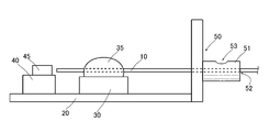
- FIG. 1 is a diagram illustrating an optical module according to a first embodiment of the present invention.
- the optical module 1 includes a base 20, a fiber mount 30 disposed on the base 20, a laser mount 40, and a semiconductor laser element 45 disposed on the laser mount 40.
- the optical fiber 10 that is partially fixed on the fiber mount 30 and the housing 50 that is connected to the base 20 and fixes another part of the optical fiber are provided as main components.
- the optical module 1 of the present embodiment is an optical module in which the optical fiber 10 is fixed to two fixing portions (a part of the fiber mount 30 and the housing 50), and is output from the semiconductor laser element 45. This is an optical module that outputs laser light to the outside of the housing 50 through the optical fiber 10. In FIG. 1, only a part of the housing 50 is shown.
- the housing 50 has a structure in which a pipe portion 51 is connected to an outer frame of a substantially rectangular parallelepiped, and the base 20 constitutes a part (bottom portion) of the housing 50.
- a through hole 52 provided in the pipe portion 51 spatially connects the inside of the housing 50 and the outside of the housing 50.
- the housing 50 is configured such that the outer frame is opened and the inside is exposed by a mechanism (not shown).
- the portion connected to the pipe portion 51 of the housing 50 is not particularly limited, but is formed by processing a plate material such as stainless steel or aluminum alloy, for example.
- the base 20 is comprised from the plate-shaped member made from a metal or a ceramic, for example.
- the metal is not particularly limited, and examples thereof include copper and copper tungsten.
- the ceramic as is not particularly limited, and examples thereof include aluminum nitride (AlN) and alumina (Al 2 O 3).
- the linear expansion coefficient of quartz constituting the optical fiber 10 is about 0.51 ⁇ 10 ⁇ 6 (1 / ° C.), but the linear expansion coefficient of the material of the base 20 is larger than this.
- copper is 16.8 ⁇ 10 ⁇ 6 (1 / ° C.
- copper tungsten (W90%) is 6.5 ⁇ 10 ⁇ 6 (1 / ° C.
- AlN is 4.5 ⁇ 10 ⁇ 6 (1 / ° C.) and Al 2 O 3 are 7.0 ⁇ 10 ⁇ 6 (1 / ° C.).
- the laser mount 40 disposed on the base 20 has a substantially rectangular parallelepiped shape, and is fixed on the base 20 with a solder material (not shown).
- the material constituting the laser mount 40 is not particularly limited, and examples thereof include ceramics such as AlN and Al 2 O 3. Among them, AlN is preferable from the viewpoint of excellent thermal conductivity. Further, when the base 20 and the laser mount 40 are made of the same ceramic, the base 20 and the laser mount 40 may be formed by integral molding.
- the semiconductor laser element 45 is fixed on the laser mount 40 with a solder material (not shown).
- a solder material not shown
- a plurality of semiconductor layers are stacked, and a resonator structure is formed by these semiconductor layers. Then, for example, laser light with a wavelength of 900 nm band is output from the surface of the semiconductor laser element 45 on the optical fiber side.
- the fiber mount 30 disposed on the base 20 has a substantially rectangular parallelepiped shape, and is fixed on the base 20 in the same manner as the laser mount.
- the material constituting the fiber mount 30 is not particularly limited.
- the same material as the material constituting the laser mount 40 can be used, and among them, AlN is preferable from the viewpoint of excellent thermal conductivity.
- the base 20 and the fiber mount 30 are made of the same ceramic, the base 20 and the fiber mount 30 may be formed by integral molding. Further, an ultraviolet curable resin 35 as a fixing member is fixed to the surface of the fiber mount 30 opposite to the base 20 side.
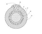
- FIG. 2 is a diagram showing a cross-sectional structure perpendicular to the longitudinal direction of the optical fiber 10 in the optical module 1.
- the optical fiber 10 includes a core 11 and a clad 12 that surrounds the outer peripheral surface of the core 11.
- the refractive index of the clad 12 is lower than the refractive index of the core 11, and the core 11 is made of glass doped with a dopant that increases the refractive index, such as germanium, and the clad 12 is doped with, for example, any dopant.
- the cladding 12 is covered with a coating layer made of an ultraviolet curable resin or the like outside the optical module 1.
- the optical fiber 10 penetrates the ultraviolet curable resin 35, and a part near the tip is fixed to the ultraviolet curable resin 35.
- the end face of the optical fiber 10 faces the emission surface of the semiconductor laser element 45, and is arranged so that the laser light output from the semiconductor laser element 45 is input to the core 11.
- FIG. 3 is a diagram showing a cross-sectional structure taken along line III-III in FIG.
- the optical fiber 10 passes through the through hole 52 of the pipe portion 51 of the housing 50 and is led out from the housing 50 to the outside of the housing 50.
- a hole 53 is provided in the pipe portion 51 in a direction perpendicular to the through hole 52, and an ultraviolet curable resin 55 is filled from the hole 53.
- the optical fiber 10 is covered with the ultraviolet curable resin 55 in the through hole 52 and fixed in the through hole 52.
- optical fiber 10 is fixed to the fiber mount 30 and the pipe portion 51 which is a part of the housing 50.
- laser light is output from the semiconductor laser element 45 by supplying electric power from the outside (not shown).
- the output laser light is input to the core 11 of the optical fiber 10, propagates through the core 11, and is output to the outside of the optical module 1.
- the optical module 1 has a predetermined guaranteed temperature range, is stored at an environmental temperature below the upper limit of the guaranteed temperature, and is used so as not to reach a temperature higher than the upper limit of the guaranteed temperature.
- the upper limit of the guaranteed temperature of the optical module 1 is set to, for example, 85 ° C. according to the characteristics of the semiconductor laser element 45 having a large temperature dependency of the laser output.
- the lower limit of the guaranteed temperature of the optical module 1 is, for example, ⁇ 20 ° C.
- FIG. 4 is a flowchart showing the steps of the method for manufacturing the optical module 1 of FIG.
- the manufacturing method of the optical module 1 includes a preparation step P1 for preparing an optical fiber 10 and an optical module semi-finished product to which the optical fiber 10 is not connected, and an end portion of the optical fiber 10 at a pipe portion 51.
- a second fixing step P4 for fixing in the through hole 52 of the pipe portion 51.
- the optical fiber 10 is prepared.
- the optical fiber has a cladding diameter of 125 ⁇ m.
- a coating layer When the optical fiber 10 is covered with a coating layer, at least the coating layer inserted into the housing 50 is peeled off.
- an optical module semi-finished product to which the optical fiber 10 is not connected is prepared.
- the housing 50 is opened to perform the subsequent steps so that the fiber mount 30 and the like in the housing 50 are exposed. deep.
- the base 20 of the casing 50 is made of copper, for example.
- First fixing step P3 a part of the optical fiber 10 arranged on the fiber mount 30 is fixed on the fiber mount 30. Specifically, in the disposing step P ⁇ b> 2, in a state where a part of the optical fiber 10 is disposed on the fiber mount 30, an ultraviolet curable resin that is a precursor of the ultraviolet curable resin 35 is changed between the optical fiber 10 and the fiber mount 30. Apply to connect to the top surface.
- the ultraviolet curable resin is cured by irradiating the ultraviolet curable resin with ultraviolet rays.
- a part of the optical fiber 10 is fixed to the fiber mount 30 with the ultraviolet curable resin 35.
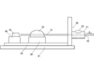
- FIG. 6 is a diagram showing a state of the second fixing step P4.
- the base 20 is heated by the heater 61.
- the temperature of the base 20 is set to t base which is equal to or higher than the upper limit of the guaranteed temperature of the optical module 1.
- the base 20 expands to a size greater than the upper limit of the guaranteed temperature by the heat from the heater 61.
- the temperature of the base 20 by the heater 61 at this time is not particularly limited as long as it is not less than the upper limit of the guaranteed temperature of the optical module 1 and does not affect the solder material or the like for fixing the semiconductor laser element 45.
- the temperature is set to 100 to 150 ° C.
- the set temperature of the heater 61 can be controlled and the temperature of the base 20 can be controlled freely.
- the optical fiber 10 is pulled in a direction indicated by an arrow A in FIG.
- tension to the optical fiber 10 By applying tension to the optical fiber 10 in this manner, the optical fiber 10 is in a state of being stretched linearly without being bent.
- the optical fiber 10 By making the optical fiber 10 be in a state of being straightly stretched without being bent, it is possible to prevent the optical fiber 10 from being subjected to excessive bending stress due to unexpected deflection.
- the tension T 0 is set so that the tension of the optical fiber 10 becomes 0 or less. determined from the linear expansion coefficient of the fiber 10, while pulling the optical fiber 10 in the tension T 0, fixing the optical fiber 10 as described later in the through hole 52 of the pipe section 51.
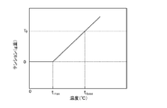
- the relationship between the temperature of the base 20 and the tension of the optical fiber 10 when the optical fiber 10 is fixed in this way is as shown in FIG. 7, below a temperature t max is shown as a tension 0, which is a compressive stress in the optical fiber 10 is applied, or the optical fiber 10 is in a state of deflected by compression stress. That is, it can be seen that by performing the second fixing step under the above-described conditions, the optical fiber 10 is subjected to compressive stress and the tensile stress is prevented from being applied throughout the guaranteed temperature range.
- the deflection amount of the optical fiber 10 allowed at the guaranteed lower temperature limit, the temperature t base in the second fixing step, and this temperature The temperature t base and the tension F at the time of fixing are set from the tension of the optical fiber 10 allowed at the time.
- the amount of bend is only an amount based on the heat shrinkage of the base that is known in advance, and it is possible to prevent the occurrence of a bend that causes cracks or the like in the fiber.
- the tension F applied to the optical fiber is, for example, 100 g weight to 200 g weight.
- the equivalent linear expansion coefficient of the base 20 is k 1
- the linear expansion coefficient of the optical fiber 10 is k 2
- the fixed temperature is t base
- the upper limit of the guaranteed temperature is t max
- the tension F applied to the fiber is , (However, A represents the cross-sectional area of the fiber, and E represents the Young's modulus of the fiber.) If it is set so as to satisfy the condition, it is possible to prevent the tensile tension from being applied to the optical fiber 10 in the entire guaranteed temperature range, and it is also possible to calculate in advance the amount of bending due to compressive stress. Can be prevented from exceeding the allowable limit.
- the relationship between the temperature of the base 20 and the tension of the optical fiber 10 as shown in FIG.
- the housing 50 other than the base 20 may act on the tension of the optical fiber 10.
- k 1 including the contribution from the casing 50 other than the base 20 is expressed as an equivalent linear expansion coefficient of the base 20.
- the optical fiber 10 is pulled to the predetermined tension to perform the fixing operation. Therefore, the optical fiber 10 is simply placed on a part of the fiber mount or the case, and compared with the case where no tension is applied. Thus, highly accurate tension management can be performed. Since the tension can be accurately set when the optical fiber 10 is fixed in this manner, the stress applied to the optical fiber 10 can be kept within a predetermined range within the guaranteed temperature range of the optical module 1, so that the optical module 1 Reliability can be improved.
- the optical fiber 10 is fixed in the through hole 52 of the pipe portion 51.
- an ultraviolet curable resin that is a precursor of the ultraviolet curable resin 55 is filled into the through hole 52 from the hole 53 formed in the pipe portion 51.
- the optical fiber 10 in the through hole 52 is covered with the filled ultraviolet curable resin.
- ultraviolet rays are irradiated into the through holes of the pipe portion 51, the ultraviolet curable resin is cured, and the optical fiber 10 is fixed in the through holes 52 of the pipe portion 51 as shown in FIG. Irradiation with ultraviolet rays may be performed by entering collimated UV light from a direction parallel to the pipe.
- the optical fiber 10 may be tensioned after filling the through hole 52 of the pipe portion 51 with an ultraviolet curable resin.
- the ultraviolet curable resin 55 is cured, and then the optical module 1 is separated from the heater, and the temperature of the optical module 1 is gradually lowered.
- casing 50 is closed as needed and the inside of the housing
- the casing 50 may be closed between the first fixing process P3 and the second fixing process P4.
- optical module 1 shown in FIG. 1 is obtained.
- the temperature of the base 20 fluctuates within the guaranteed temperature range of the optical module 1 due to the environmental temperature during storage and the heat generation during operation, and the base 20 expands thermally.
- a part of the optical fiber 10 is fixed to the fiber mount 30, and the base 20 is heated above the upper limit of the guaranteed temperature of the optical module 1.
- the manufactured optical module 1 is within the guaranteed temperature range.
- the optical module 1 manufactured by the method for manufacturing the optical module 1 according to the present embodiment can prevent the optical fiber 10 from being broken and the optical fiber 10 from being cracked, and has excellent reliability. Can do.
- the second fixing step P4 is performed after the first fixing step P3. However, at least a part of the first fixing step P3 and the second fixing step P4 may be performed simultaneously.
- FIG. 8 is a plan view showing an optical module 2 according to the second embodiment of the present invention.
- a part of the optical fiber 1 is fixed on the fiber mount 30 by the solder 36 and the other part is pipe 51 by the solder 56. This is different from the optical module 1 of the first embodiment in that it is fixed in the through hole 52.
- a bonding pad 31 is formed on the surface of the fiber mount 30 opposite to the base 20 side.
- the bonding pad 31 is not particularly limited as long as it is a material to which the solder 36 can be fixed.
- a titanium (Ti) layer is laminated on the fiber mount 30 side, and platinum (Pt) is formed on the Ti layer.
- the gold (Au) layer is laminated on the Pt layer, and the surface of the Au layer is the surface opposite to the fiber mount 30 side of the bonding pad 31.
- the solder 36 is fixed on the bonding pad 31 and covers the optical fiber 10 on the bonding pad 31. Thus, the optical fiber 10 is fixed on the fiber mount by the solder 36.
- the through hole 52 of the pipe part 51 into which the optical fiber 10 is inserted is filled with solder 56 from the hole 53 of the pipe part 51, and the optical fiber 10 is inserted into the through hole 52 by the solder 56. It is covered and fixed in the through hole 52.
- solders 36 and 56 examples include gold-tin eutectic solder, and the ratio of Au and tin (Sn) includes Au 80% -Sn 20% and Au 10% -Sn 90%. it can. When the solder 36 is Au 80% -Sn 20%, the melting point of the solder 36 is about 280 degrees.
- the optical fiber 10 is covered with a metallization layer (not shown) on the bonding pad 31 and in the through hole 52, and the metallization layer is fixed to the solders 36 and 56.
- the metallized layer is configured to be easily wetted and fixed to the solders 36 and 56 and is not particularly limited.
- the metallized layer is formed of a laminate of a Ni layer and an Au layer, and the Ni layer covers the outer peripheral surface of the clad 12.
- the Au layer covers the outer peripheral surface of the Ni layer.
- the thicknesses of the Ni layer and the Au layer are not particularly limited.
- the Ni layer is 2 ⁇ m to 3 ⁇ m
- the Au layer is 0.1 ⁇ m to 0.2 ⁇ m.
- the surface of the metallized layer is composed of the Au layer because the solder wettability of the metallized layer is enhanced even without flux.
- Such an optical module 2 is manufactured as follows.
- the preparation process P1 is performed as in the first embodiment.
- a bonding pad 31 is provided on the fiber mount 30 when preparing an optical module semi-finished product to which no optical fiber is connected.
- the bonding pad 31 may be formed by a film forming process such as vapor deposition, sputtering, or plating.
- a metallized layer is formed in a portion located on the bonding pad 31 in the optical fiber 10 and a portion located in the through hole 52 of the pipe portion 51.
- the metallized layer is preferably formed by a plating method. This is because according to the plating method, the metallized layer can be provided with a more uniform thickness on the side surface of the optical fiber 10 having a cylindrical shape on the side surface.
- First fixing step P3 Next, the first fixing process P3 is performed.
- the first fixing step P ⁇ b> 3 first, a lump of solder 36 is disposed on the bonding pad 31 so as to be adjacent to the optical fiber 10. Thereafter, the fiber mount 30 is irradiated with laser light to heat the fiber mount 30. Due to the heat of the fiber mount 30, the solder 36 on the bonding pad 31 is melted and spreads over the entire bonding pad 31, and covers the metallized layer of the optical fiber 10. Then, by stopping the laser light irradiation, the temperature of the fiber mount 30 is lowered, and a part of the optical fiber 10 is fixed on the fiber mount 30.
- the second fixing step P4 is performed.
- a lump of solder 56 is disposed on the hole 53 of the pipe portion 51.
- the pipe part 51 is heated by high frequency induction heating.
- the base 20 is heated simultaneously by this high frequency induction heating.
- the tension F is applied to the optical fiber 10 in the same manner as in the first embodiment.
- the solder 56 on the hole 53 is melted, and the solder 56 is filled in the through hole 52 of the pipe portion 51. Thereafter, the heating is stopped and the solder 56 is solidified, whereby the optical fiber 10 is fixed to the pipe portion 51.
- the second fixing step P4 by heating the base 20 with heat that melts the solder 56, there is no need to heat the base 20 by other means, thereby simplifying the manufacturing process. be able to.
- the second fixing step P4 is performed by high-frequency induction heating, but the second fixing step P4 may be performed by resistance heating or heating by laser light.
- the base 20 is heated by heat that melts the solder 56.
- the base 20 may be heated by a heater in the same manner as in the first embodiment.
- dissolves the solder 56 may be sufficient.
- the fiber mount 30 is irradiated with laser light and the solder 36 is melted by the heat of the fiber mount 30, but also in the first fixing step P3, the solder 36 is melted by resistance heating.
- the solder 36 may be melted by high frequency induction heating.
- the tension F given to the optical fiber in the second fixing step P4 may be given before heating.
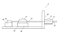
- FIG. 9 is a plan view showing an optical module 3 according to the third embodiment of the present invention.
- a part of the optical fiber 1 is fixed on the fiber mount 30 by the thermosetting resin 37 and the other part is thermosetting. It differs from the optical module 1 of the first embodiment in that it is fixed in the through hole 52 of the pipe part 51 by the resin 57.
- Such an optical module 3 is manufactured as follows.
- preparation process P1 is performed as in the first embodiment.
- positioning process P2 is performed like 1st Embodiment.
- First fixing step P3 a part of the optical fiber 10 disposed on the fiber mount 30 is fixed on the fiber mount. Specifically, in the placement step P2, in a state where the optical fiber 10 is placed on the fiber mount 30, an uncured thermosetting resin is applied so as to connect the optical fiber 10 and the upper surface of the fiber mount 30. To do.
- thermosetting resin is heated by a heater to cure the thermosetting resin.
- a part of the optical fiber 10 is fixed to the fiber mount 30 with the thermosetting resin 37.
- thermosetting resin is filled into the through hole 52 from the hole 53 formed in the pipe portion 51, and the optical fiber 10 in the through hole 52 is covered with the thermosetting resin. And while heating the pipe part 51 with a heater, the base 20 is heated, In the state in which the temperature of the base 20 became more than the upper limit of the guarantee temperature of the optical module 2, it was carried out similarly to 1st Embodiment, A tension F is applied to the optical fiber 10.
- the curing temperature of the thermosetting resin 57 is the optical module 2's.
- the temperature is higher than the upper limit of the guaranteed temperature. Since this tension needs to be applied before the uncured thermosetting resin is cured, the tension is preferably applied before heating.
- the optical fiber 10 is fixed in the through hole 52 of the pipe portion 51 by the thermosetting resin 57 thus cured, and the optical module shown in FIG. 9 is obtained.
- the second fixing step P4 by heating the base 20 with heat that cures the uncured thermosetting resin, there is no need to heat the base 20 by other means, and manufacturing The process can be simplified.
- the second fixing step P4 is performed with a heater, but the thermosetting resin may be heated by other means. Further, the base 20 may be heated using a heater different from the heater for curing the thermosetting resin.
- thermosetting resin may be cured by other means.
- the optical module that outputs the laser light output from the semiconductor laser element by an optical fiber has been described as an example.
- the present invention is not limited to this, and the optical fiber is fixed to two fixing portions.
- the optical module manufacturing method can be applied to other optical modules.
- it can also be used for an optical module such as a LiNbO 3 modulator of a type in which an optical fiber is fixed to two fixing portions.
- the member for fixing the optical fiber 10 may be other than the member in the above-described embodiment, and for example, glass frit or thermoplastic resin may be used. .
- an optical module manufacturing method capable of manufacturing an optical module having excellent reliability is provided.
Landscapes
- Physics & Mathematics (AREA)
- General Physics & Mathematics (AREA)
- Optics & Photonics (AREA)
- Optical Couplings Of Light Guides (AREA)
- Semiconductor Lasers (AREA)
Abstract
L'invention porte sur un procédé de fabrication pour un module optique, par lequel procédé il est possible de fabriquer un module optique hautement fiable. Grâce au procédé de fabrication pour un module optique (1), un module optique ayant des fibres optiques (10) fixées en deux sections de fixation (une monture de fibres (30) et une partie de tuyau (51)) est fabriqué. Ce procédé comprend : une première étape de fixation (P3) pour fixer une partie de la fibre optique (10) sur la monture de fibres (30) ; et une seconde étape de fixation (P4) pour tirer, dans un état dans lequel une base (20) reliée à chaque section de fixation est chauffée au-dessus de la limite supérieure de la température garantie du module optique (1), la fibre optique (10), tout en appliquant une tension à celle-ci, et fixer l'autre partie de la fibre optique (10) sur la partie de tuyau (51).
Priority Applications (4)
| Application Number | Priority Date | Filing Date | Title |
|---|---|---|---|
| EP12770849.3A EP2698656A4 (fr) | 2011-04-13 | 2012-02-24 | Procédé de fabrication pour module optique |
| CN2012800143822A CN103443681A (zh) | 2011-04-13 | 2012-02-24 | 光模块的制造方法 |
| JP2013509821A JP5810153B2 (ja) | 2011-04-13 | 2012-02-24 | 光モジュールの製造方法 |
| US14/051,981 US9335489B2 (en) | 2011-04-13 | 2013-10-11 | Manufacturing method for optical module |
Applications Claiming Priority (2)
| Application Number | Priority Date | Filing Date | Title |
|---|---|---|---|
| JP2011-089363 | 2011-04-13 | ||
| JP2011089363 | 2011-04-13 |
Related Child Applications (1)
| Application Number | Title | Priority Date | Filing Date |
|---|---|---|---|
| US14/051,981 Continuation US9335489B2 (en) | 2011-04-13 | 2013-10-11 | Manufacturing method for optical module |
Publications (1)
| Publication Number | Publication Date |
|---|---|
| WO2012140958A1 true WO2012140958A1 (fr) | 2012-10-18 |
Family
ID=47009140
Family Applications (1)
| Application Number | Title | Priority Date | Filing Date |
|---|---|---|---|
| PCT/JP2012/054623 Ceased WO2012140958A1 (fr) | 2011-04-13 | 2012-02-24 | Procédé de fabrication pour module optique |
Country Status (5)
| Country | Link |
|---|---|
| US (1) | US9335489B2 (fr) |
| EP (1) | EP2698656A4 (fr) |
| JP (1) | JP5810153B2 (fr) |
| CN (1) | CN103443681A (fr) |
| WO (1) | WO2012140958A1 (fr) |
Families Citing this family (2)
| Publication number | Priority date | Publication date | Assignee | Title |
|---|---|---|---|---|
| JP5905563B1 (ja) | 2014-12-01 | 2016-04-20 | 株式会社フジクラ | 半導体レーザモジュールの製造方法 |
| CN104698551A (zh) * | 2015-03-10 | 2015-06-10 | 武汉电信器件有限公司 | 光纤耦合的多模半导体光电器件 |
Citations (3)
| Publication number | Priority date | Publication date | Assignee | Title |
|---|---|---|---|---|
| JPH0273207A (ja) * | 1988-09-09 | 1990-03-13 | Nippon Telegr & Teleph Corp <Ntt> | 光導波路部品の実装構造 |
| JPH04152308A (ja) * | 1990-10-16 | 1992-05-26 | Anritsu Corp | 光ファイバ装置及び光ファイバ固定方法 |
| JPH11174261A (ja) * | 1997-12-11 | 1999-07-02 | Furukawa Electric Co Ltd:The | 光ファイバの固定方法および該固定方法に用いる固定用治具 |
Family Cites Families (20)
| Publication number | Priority date | Publication date | Assignee | Title |
|---|---|---|---|---|
| WO1986007149A1 (fr) * | 1985-05-29 | 1986-12-04 | Kurt Tiefenthaler | Senseur optique pour etablir selectivement la presence de substances ainsi que la variation d'indice de refraction dans les substances objet de mesures |
| EP0403468A1 (fr) * | 1988-02-14 | 1990-12-27 | LUKOSZ, Walter | Procede optique integre d'interference |
| US5442169A (en) * | 1991-04-26 | 1995-08-15 | Paul Scherrer Institut | Method and apparatus for determining a measuring variable by means of an integrated optical sensor module |
| US5754714A (en) * | 1994-09-17 | 1998-05-19 | Kabushiki Kaisha Toshiba | Semiconductor optical waveguide device, optical control type optical switch, and wavelength conversion device |
| US5623561A (en) * | 1995-09-29 | 1997-04-22 | Georgia Tech Research Corporation | Integrated optic interferometric sensor |
| GB2340620B (en) | 1998-08-12 | 2002-12-31 | Bookham Technology Ltd | Manufacture of an optics package |
| JP2000266943A (ja) * | 1999-03-12 | 2000-09-29 | Nippon Electric Glass Co Ltd | 光通信用温度補償デバイス |
| US6821027B2 (en) * | 2000-10-16 | 2004-11-23 | Opti Japan Corporation | Miniaturized parallel optical transmitter and receiver module |
| JP3720790B2 (ja) * | 2002-04-18 | 2005-11-30 | 川崎重工業株式会社 | 光伝達媒体が埋設される構造体の製造方法 |
| NO339298B1 (no) * | 2003-10-10 | 2016-11-21 | Optoplan As | Aktiv koherensreduksjon for interferometeravspørring |
| CN100432723C (zh) * | 2004-03-31 | 2008-11-12 | 日立化成工业株式会社 | 光学元件耦合结构体及光纤结构体 |
| JP2006071300A (ja) * | 2004-08-31 | 2006-03-16 | Hitachi Ltd | 生化学物質検出装置 |
| US7421200B2 (en) * | 2004-12-09 | 2008-09-02 | Intel Corporation | Reduced loss ultra-fast semiconductor modulator and switch |
| JP4615414B2 (ja) * | 2005-09-30 | 2011-01-19 | 住友電工デバイス・イノベーション株式会社 | 光モジュール |
| US7256929B1 (en) * | 2006-01-20 | 2007-08-14 | Intel Corporation | Semiconductor waveguide based high speed all optical wavelength converter |
| JP4810393B2 (ja) * | 2006-10-27 | 2011-11-09 | 富士通株式会社 | 光モジュール製造方法及び製造装置 |
| JP2009288509A (ja) * | 2008-05-29 | 2009-12-10 | Fujitsu Ltd | 光変調装置 |
| WO2010110068A1 (fr) * | 2009-03-25 | 2010-09-30 | 古河電気工業株式会社 | Module de laser semi-conducteur et son procédé de fabrication |
| KR101313236B1 (ko) * | 2009-12-11 | 2013-09-30 | 한국전자통신연구원 | 광섬유 레이저 |
| CN102844943A (zh) * | 2010-03-31 | 2012-12-26 | 株式会社藤仓 | 激光装置 |
-
2012
- 2012-02-24 WO PCT/JP2012/054623 patent/WO2012140958A1/fr not_active Ceased
- 2012-02-24 JP JP2013509821A patent/JP5810153B2/ja active Active
- 2012-02-24 CN CN2012800143822A patent/CN103443681A/zh active Pending
- 2012-02-24 EP EP12770849.3A patent/EP2698656A4/fr not_active Withdrawn
-
2013
- 2013-10-11 US US14/051,981 patent/US9335489B2/en active Active
Patent Citations (3)
| Publication number | Priority date | Publication date | Assignee | Title |
|---|---|---|---|---|
| JPH0273207A (ja) * | 1988-09-09 | 1990-03-13 | Nippon Telegr & Teleph Corp <Ntt> | 光導波路部品の実装構造 |
| JPH04152308A (ja) * | 1990-10-16 | 1992-05-26 | Anritsu Corp | 光ファイバ装置及び光ファイバ固定方法 |
| JPH11174261A (ja) * | 1997-12-11 | 1999-07-02 | Furukawa Electric Co Ltd:The | 光ファイバの固定方法および該固定方法に用いる固定用治具 |
Non-Patent Citations (1)
| Title |
|---|
| See also references of EP2698656A4 * |
Also Published As
| Publication number | Publication date |
|---|---|
| US9335489B2 (en) | 2016-05-10 |
| CN103443681A (zh) | 2013-12-11 |
| JPWO2012140958A1 (ja) | 2014-07-28 |
| EP2698656A4 (fr) | 2014-08-27 |
| US20140059831A1 (en) | 2014-03-06 |
| JP5810153B2 (ja) | 2015-11-11 |
| EP2698656A1 (fr) | 2014-02-19 |
Similar Documents
| Publication | Publication Date | Title |
|---|---|---|
| CN1328798C (zh) | 光电子元件和制造方法 | |
| JP4050402B2 (ja) | 光電子装置およびその製造方法 | |
| JP2011095295A (ja) | 光モジュールの光ファイバブロックおよびその製造方法 | |
| JP2015045875A (ja) | 溶接接合方法及び溶接接合されたコンポーネントを有するデバイス | |
| JP5810153B2 (ja) | 光モジュールの製造方法 | |
| CN108508545B (zh) | 光学器件的耦合结构及耦合方法 | |
| JP5636377B2 (ja) | 電磁線伝送用の光導波路及びその製造方法 | |
| US20140348463A1 (en) | Optical device and method for manufacuturing the optical device | |
| US9488785B2 (en) | Optical subassembly, optical system and method | |
| JPH0850223A (ja) | 光学的プリンタヘッド | |
| JP2018004830A (ja) | 高耐熱性光ファイバモジュールおよびその作製方法 | |
| WO2013128728A1 (fr) | Module optique et procédé de production pour celui-ci | |
| JP5102380B2 (ja) | ファイバマウント装置、及び、それを用いた光モジュール、及び、光モジュールの製造方法 | |
| JP2009093041A (ja) | 光モジュール | |
| JP6279352B2 (ja) | 光結合部品、光コネクタおよび光結合方法 | |
| JP5982457B2 (ja) | 光モジュールの製造方法 | |
| JP2012182367A (ja) | 部品搭載方法および部品搭載装置 | |
| JP2007271674A (ja) | 光デバイス | |
| JP2015125362A (ja) | 光ファイバ | |
| JP5508249B2 (ja) | 光モジュールの製造方法 | |
| WO2013018426A1 (fr) | Procédé de fabrication d'un module laser et dispositif de préhension de fibre optique utilisé dans ce dernier | |
| JP2017120282A (ja) | 融着接続部補強構造および融着接続部補強構造の製造方法 | |
| JP2019174541A (ja) | 光モジュール | |
| JP5905563B1 (ja) | 半導体レーザモジュールの製造方法 | |
| JP2017044761A (ja) | 光モジュール及びその作製方法 |
Legal Events
| Date | Code | Title | Description |
|---|---|---|---|
| 121 | Ep: the epo has been informed by wipo that ep was designated in this application |
Ref document number: 12770849 Country of ref document: EP Kind code of ref document: A1 |
|
| ENP | Entry into the national phase |
Ref document number: 2013509821 Country of ref document: JP Kind code of ref document: A |
|
| NENP | Non-entry into the national phase |
Ref country code: DE |
|
| WWE | Wipo information: entry into national phase |
Ref document number: 2012770849 Country of ref document: EP |