WO2012140987A1 - Dispositif de séparation, système de séparation et procédé de séparation - Google Patents
Dispositif de séparation, système de séparation et procédé de séparation Download PDFInfo
- Publication number
- WO2012140987A1 WO2012140987A1 PCT/JP2012/056864 JP2012056864W WO2012140987A1 WO 2012140987 A1 WO2012140987 A1 WO 2012140987A1 JP 2012056864 W JP2012056864 W JP 2012056864W WO 2012140987 A1 WO2012140987 A1 WO 2012140987A1
- Authority
- WO
- WIPO (PCT)
- Prior art keywords
- substrate
- processed
- holding
- wafer
- inert gas
- Prior art date
- Legal status (The legal status is an assumption and is not a legal conclusion. Google has not performed a legal analysis and makes no representation as to the accuracy of the status listed.)
- Ceased
Links
Images















Classifications
-
- B—PERFORMING OPERATIONS; TRANSPORTING
- B32—LAYERED PRODUCTS
- B32B—LAYERED PRODUCTS, i.e. PRODUCTS BUILT-UP OF STRATA OF FLAT OR NON-FLAT, e.g. CELLULAR OR HONEYCOMB, FORM
- B32B38/00—Ancillary operations in connection with laminating processes
- B32B38/10—Removing layers, or parts of layers, mechanically or chemically
-
- H—ELECTRICITY
- H10—SEMICONDUCTOR DEVICES; ELECTRIC SOLID-STATE DEVICES NOT OTHERWISE PROVIDED FOR
- H10P—GENERIC PROCESSES OR APPARATUS FOR THE MANUFACTURE OR TREATMENT OF DEVICES COVERED BY CLASS H10
- H10P72/00—Handling or holding of wafers, substrates or devices during manufacture or treatment thereof
- H10P72/04—Apparatus for manufacture or treatment
- H10P72/0428—Apparatus for mechanical treatment or grinding or cutting
-
- B—PERFORMING OPERATIONS; TRANSPORTING
- B32—LAYERED PRODUCTS
- B32B—LAYERED PRODUCTS, i.e. PRODUCTS BUILT-UP OF STRATA OF FLAT OR NON-FLAT, e.g. CELLULAR OR HONEYCOMB, FORM
- B32B43/00—Operations specially adapted for layered products and not otherwise provided for, e.g. repairing; Apparatus therefor
- B32B43/006—Delaminating
-
- H—ELECTRICITY
- H10—SEMICONDUCTOR DEVICES; ELECTRIC SOLID-STATE DEVICES NOT OTHERWISE PROVIDED FOR
- H10P—GENERIC PROCESSES OR APPARATUS FOR THE MANUFACTURE OR TREATMENT OF DEVICES COVERED BY CLASS H10
- H10P72/00—Handling or holding of wafers, substrates or devices during manufacture or treatment thereof
- H10P72/04—Apparatus for manufacture or treatment
- H10P72/0431—Apparatus for thermal treatment
- H10P72/0434—Apparatus for thermal treatment mainly by convection
-
- H—ELECTRICITY
- H10—SEMICONDUCTOR DEVICES; ELECTRIC SOLID-STATE DEVICES NOT OTHERWISE PROVIDED FOR
- H10P—GENERIC PROCESSES OR APPARATUS FOR THE MANUFACTURE OR TREATMENT OF DEVICES COVERED BY CLASS H10
- H10P72/00—Handling or holding of wafers, substrates or devices during manufacture or treatment thereof
- H10P72/04—Apparatus for manufacture or treatment
- H10P72/0448—Apparatus for applying a liquid, a resin, an ink or the like
-
- H—ELECTRICITY
- H10—SEMICONDUCTOR DEVICES; ELECTRIC SOLID-STATE DEVICES NOT OTHERWISE PROVIDED FOR
- H10P—GENERIC PROCESSES OR APPARATUS FOR THE MANUFACTURE OR TREATMENT OF DEVICES COVERED BY CLASS H10
- H10P72/00—Handling or holding of wafers, substrates or devices during manufacture or treatment thereof
- H10P72/30—Handling or holding of wafers, substrates or devices during manufacture or treatment thereof for conveying, e.g. between different workstations
- H10P72/33—Handling or holding of wafers, substrates or devices during manufacture or treatment thereof for conveying, e.g. between different workstations into and out of processing chamber
- H10P72/3306—Horizontal transfer of a single workpiece
-
- B—PERFORMING OPERATIONS; TRANSPORTING
- B32—LAYERED PRODUCTS
- B32B—LAYERED PRODUCTS, i.e. PRODUCTS BUILT-UP OF STRATA OF FLAT OR NON-FLAT, e.g. CELLULAR OR HONEYCOMB, FORM
- B32B2457/00—Electrical equipment
- B32B2457/14—Semiconductor wafers
-
- Y—GENERAL TAGGING OF NEW TECHNOLOGICAL DEVELOPMENTS; GENERAL TAGGING OF CROSS-SECTIONAL TECHNOLOGIES SPANNING OVER SEVERAL SECTIONS OF THE IPC; TECHNICAL SUBJECTS COVERED BY FORMER USPC CROSS-REFERENCE ART COLLECTIONS [XRACs] AND DIGESTS
- Y10—TECHNICAL SUBJECTS COVERED BY FORMER USPC
- Y10T—TECHNICAL SUBJECTS COVERED BY FORMER US CLASSIFICATION
- Y10T156/00—Adhesive bonding and miscellaneous chemical manufacture
- Y10T156/11—Methods of delaminating, per se; i.e., separating at bonding face
- Y10T156/1126—Using direct fluid current against work during delaminating
- Y10T156/1137—Using air blast directly against work during delaminating
-
- Y—GENERAL TAGGING OF NEW TECHNOLOGICAL DEVELOPMENTS; GENERAL TAGGING OF CROSS-SECTIONAL TECHNOLOGIES SPANNING OVER SEVERAL SECTIONS OF THE IPC; TECHNICAL SUBJECTS COVERED BY FORMER USPC CROSS-REFERENCE ART COLLECTIONS [XRACs] AND DIGESTS
- Y10—TECHNICAL SUBJECTS COVERED BY FORMER USPC
- Y10T—TECHNICAL SUBJECTS COVERED BY FORMER US CLASSIFICATION
- Y10T156/00—Adhesive bonding and miscellaneous chemical manufacture
- Y10T156/11—Methods of delaminating, per se; i.e., separating at bonding face
- Y10T156/1153—Temperature change for delamination [e.g., heating during delaminating, etc.]
-
- Y—GENERAL TAGGING OF NEW TECHNOLOGICAL DEVELOPMENTS; GENERAL TAGGING OF CROSS-SECTIONAL TECHNOLOGIES SPANNING OVER SEVERAL SECTIONS OF THE IPC; TECHNICAL SUBJECTS COVERED BY FORMER USPC CROSS-REFERENCE ART COLLECTIONS [XRACs] AND DIGESTS
- Y10—TECHNICAL SUBJECTS COVERED BY FORMER USPC
- Y10T—TECHNICAL SUBJECTS COVERED BY FORMER US CLASSIFICATION
- Y10T156/00—Adhesive bonding and miscellaneous chemical manufacture
- Y10T156/11—Methods of delaminating, per se; i.e., separating at bonding face
- Y10T156/1168—Gripping and pulling work apart during delaminating
- Y10T156/1189—Gripping and pulling work apart during delaminating with shearing during delaminating
-
- Y—GENERAL TAGGING OF NEW TECHNOLOGICAL DEVELOPMENTS; GENERAL TAGGING OF CROSS-SECTIONAL TECHNOLOGIES SPANNING OVER SEVERAL SECTIONS OF THE IPC; TECHNICAL SUBJECTS COVERED BY FORMER USPC CROSS-REFERENCE ART COLLECTIONS [XRACs] AND DIGESTS
- Y10—TECHNICAL SUBJECTS COVERED BY FORMER USPC
- Y10T—TECHNICAL SUBJECTS COVERED BY FORMER US CLASSIFICATION
- Y10T156/00—Adhesive bonding and miscellaneous chemical manufacture
- Y10T156/19—Delaminating means
- Y10T156/1911—Heating or cooling delaminating means [e.g., melting means, freezing means, etc.]
-
- Y—GENERAL TAGGING OF NEW TECHNOLOGICAL DEVELOPMENTS; GENERAL TAGGING OF CROSS-SECTIONAL TECHNOLOGIES SPANNING OVER SEVERAL SECTIONS OF THE IPC; TECHNICAL SUBJECTS COVERED BY FORMER USPC CROSS-REFERENCE ART COLLECTIONS [XRACs] AND DIGESTS
- Y10—TECHNICAL SUBJECTS COVERED BY FORMER USPC
- Y10T—TECHNICAL SUBJECTS COVERED BY FORMER US CLASSIFICATION
- Y10T156/00—Adhesive bonding and miscellaneous chemical manufacture
- Y10T156/19—Delaminating means
- Y10T156/1928—Differential fluid pressure delaminating means
- Y10T156/1933—Spraying delaminating means [e.g., atomizer, etc.
- Y10T156/1939—Air blasting delaminating means]
-
- Y—GENERAL TAGGING OF NEW TECHNOLOGICAL DEVELOPMENTS; GENERAL TAGGING OF CROSS-SECTIONAL TECHNOLOGIES SPANNING OVER SEVERAL SECTIONS OF THE IPC; TECHNICAL SUBJECTS COVERED BY FORMER USPC CROSS-REFERENCE ART COLLECTIONS [XRACs] AND DIGESTS
- Y10—TECHNICAL SUBJECTS COVERED BY FORMER USPC
- Y10T—TECHNICAL SUBJECTS COVERED BY FORMER US CLASSIFICATION
- Y10T156/00—Adhesive bonding and miscellaneous chemical manufacture
- Y10T156/19—Delaminating means
- Y10T156/1961—Severing delaminating means [e.g., chisel, etc.]
- Y10T156/1967—Cutting delaminating means
- Y10T156/1972—Shearing delaminating means
Definitions
- the present invention relates to a peeling device for peeling a polymerized substrate from a substrate to be processed and a support substrate, a peeling system provided with the peeling device, and a peeling method using the peeling device.
- the diameter of a semiconductor wafer (hereinafter referred to as “wafer”) has been increased. Further, in a specific process such as mounting, it is required to make the wafer thinner. For example, if a thin wafer having a large diameter is transported or polished as it is, the wafer may be warped or cracked. For this reason, in order to reinforce the wafer, for example, the wafer is attached to a wafer or a glass substrate which is a support substrate. Then, after a predetermined process such as a wafer polishing process is performed in a state where the wafer and the support substrate are bonded in this way, the wafer and the support substrate are peeled off.
- a predetermined process such as a wafer polishing process is performed in a state where the wafer and the support substrate are bonded in this way, the wafer and the support substrate are peeled off.
- Patent Document 1 proposes a peeling apparatus that directly bonds a wafer on which a device is formed to a support substrate on which a thermal oxide film is formed, and then peels the wafer.
- This peeling apparatus has, for example, a first holder that holds a wafer, a second holder that holds a support substrate, and a nozzle that ejects liquid between the wafer and the support substrate.
- an injection pressure preferably a bonding pressure
- between the wafer and the support substrate bonded from the nozzle that is, on the bonding surface between the wafer and the support substrate, is larger than the bonding strength between the wafer and the support substrate. Separation of the wafer and the support substrate is performed by ejecting the liquid with an ejection pressure that is twice or more larger than the strength.
- the device may be formed not only on the bonding surface of the wafer bonded to the support substrate but also on the surface opposite to the bonding surface and on the non-bonding surface of the wafer held by the first holder. .
- a gap is generated between the holding surface of the first holder and the non-bonding surface of the wafer, and a part of the non-bonding surface of the wafer is exposed.
- ambient air also flows from this gap. For this reason, as described above, in the heated wafer, the exposed non-bonded surface is oxidized.
- the present invention has been made in view of the above points, and an object of the present invention is to suppress oxidation of a non-joint surface of a substrate to be processed at the time of peeling treatment between the substrate to be processed and a supporting substrate accompanied by heat treatment. .
- the present invention is a peeling apparatus for peeling a polymerized substrate in which a substrate to be processed and a support substrate are bonded with an adhesive to the substrate to be processed and the support substrate, and heating the substrate to be processed.
- a first holding portion that includes a heating mechanism and holds the substrate to be processed; a second holding portion that includes a heating mechanism that heats the support substrate and holds the support substrate; and at least the first holding portion
- a moving mechanism for moving the portion or the second holding portion relatively in the horizontal direction, and an annular shape along the outer peripheral portion of the first holding portion, and a plurality of holes are formed.
- a porous portion that supplies an inert gas to the outer peripheral portion of the held first holding portion.
- the first holding unit and the second holding unit are moved by the moving mechanism while heating the substrate to be processed held by the first holding unit and the support substrate held by the second holding unit.
- the substrate to be processed and the support substrate can be separated by moving the substrate relatively in the horizontal direction.
- an inert gas can be supplied from the porous part to the outer peripheral portion of the first holding unit.
- the inert gas is supplied from the porous portion in which a plurality of holes are formed, the flow rate of the inert gas is suppressed. Thereby, only inert gas is supplied to the outer peripheral part of a 1st holding
- a peeling system including a peeling device that peels a polymerized substrate in which a substrate to be processed and a support substrate are bonded with an adhesive, to the substrate to be processed and the support substrate.
- a first holding unit that includes a heating mechanism that heats the substrate to be processed, and a second holding unit that includes a heating mechanism that heats the support substrate and holds the support substrate;
- a moving mechanism that moves at least the first holding part or the second holding part in a relatively horizontal direction and an annular shape that is provided along the outer peripheral part of the first holding part, and forms a plurality of holes
- a porous portion that supplies an inert gas to the outer peripheral portion of the first holding portion that holds the substrate to be processed, and the peeling system is peeled off by the peeling device
- Another aspect of the present invention is a peeling method for peeling a polymerized substrate in which a substrate to be processed and a support substrate are bonded with an adhesive using a peeling device to the substrate to be processed and the support substrate.
- a heating mechanism that heats the substrate to be processed
- a first holding portion that holds the substrate to be processed
- a second holding portion that includes a heating mechanism that heats the support substrate and holds the support substrate.
- the oxidation of the non-joint surface of the substrate to be processed can be suppressed during the peeling process between the substrate to be processed and the support substrate accompanied by the heat treatment.
- FIG. 1 is a plan view showing an outline of a configuration of a peeling system 1 according to the present embodiment.
- a superposed wafer T as a superposed substrate in which a target wafer W as a target substrate and a support wafer S as a support substrate are bonded with an adhesive G is used as a target wafer W. And the support wafer S is peeled off.
- a surface bonded to the support wafer S via the adhesive G is referred to as “bonding surface W J ”, and a surface opposite to the bonding surface W J is referred to as “non-bonding surface W N ”. That's it.
- the support wafer S, the surface to be bonded to the wafer W through the adhesive G is referred to as "bonding surface S J", while the opposite side of the surface as the joint surface S J "non-bonding surface S N "
- wafer W is a wafer as a product, a plurality of devices are formed, for example, joint surface W J and a non-bonding surface W N.
- the wafer W is, for example, non-bonding surface W N is polished, thin (e.g., thickness of 50 [mu] m) it is.
- the support wafer S is a wafer having the same diameter as the wafer W to be processed and supporting the wafer W to be processed. In this embodiment, the case where a wafer is used as the support substrate will be described, but another substrate such as a glass substrate may be used.
- the peeling system 1 includes cassettes C W , C S , and C T that can accommodate, for example, a plurality of wafers W to be processed, a plurality of support wafers S, and a plurality of superposed wafers T, respectively.
- the interface station 5 that transfers the wafer W to be processed to and from the station 4 is integrally connected.
- the loading / unloading station 2 and the peeling treatment station 3 are arranged side by side in the X direction (vertical direction in FIG. 1).
- a wafer transfer region 6 is formed between the carry-in / out station 2 and the peeling processing station 3.
- the interface station 5 is disposed on the Y direction negative direction side (left direction side in FIG. 1) of the peeling processing station 3.
- An inspection apparatus 7 for inspecting the wafer W to be processed before being transferred to the post-processing station 4 is disposed on the positive side in the X direction of the interface station 5 (upward in FIG. 1).
- post-inspection cleaning for cleaning the processed wafer W after inspection is performed on the opposite side of the inspection apparatus 7 across the interface station 5, that is, on the negative side in the X direction of the interface station 5 (downward side in FIG. 1).
- a device 8 is arranged.
- the loading / unloading station 2 is provided with a cassette mounting table 10.
- a plurality of, for example, three cassette mounting plates 11 are provided on the cassette mounting table 10.
- the cassette mounting plates 11 are arranged in a line in the Y direction (left and right direction in FIG. 1). These cassette mounting plates 11, cassettes C W to the outside of the peeling system 1, C S, when loading and unloading the C T, a cassette C W, C S, can be placed on C T .
- the carry-in / out station 2 is configured to be capable of holding a plurality of wafers W to be processed, a plurality of support wafers S, and a plurality of superposed wafers T.
- the number of cassette mounting plates 11 is not limited to the present embodiment, and can be arbitrarily determined.
- a plurality of superposed wafers T carried into the carry-in / out station 2 are inspected in advance, and a superposed wafer T including a normal processing target wafer W and a superposed wafer T including a defective target processing wafer W. And have been determined.
- the first transfer device 20 is disposed in the wafer transfer region 6.
- the first transfer device 20 includes a transfer arm that can move around, for example, a vertical direction, a horizontal direction (Y direction, X direction), and a vertical axis.
- the first transfer device 20 moves in the wafer transfer region 6 and can transfer the wafer W to be processed, the support wafer S, and the overlapped wafer T between the carry-in / out station 2 and the separation processing station 3.
- the peeling processing station 3 has a peeling device 30 that peels the superposed wafer T into the processing target wafer W and the supporting wafer S.
- a first cleaning device 31 that cleans the wafer to be processed W that has been peeled off is disposed on the negative side in the Y direction of the peeling device 30 (left side in FIG. 1).
- a second transfer device 32 is provided between the peeling device 30 and the first cleaning device 31.
- a second cleaning device 33 for cleaning the peeled support wafer S is arranged on the positive side in the Y direction of the peeling device 30 (right side in FIG. 1).
- the first cleaning device 31, the second transport device 32, the peeling device 30, and the second cleaning device 33 are arranged in this order from the interface station 5 side in the peeling processing station 3.
- the inspection device 7 the presence or absence of a residue of the adhesive G on the processing target wafer W peeled by the peeling device 30 is inspected. Further, in the post-inspection cleaning apparatus 8, the wafer W to be processed in which the residue of the adhesive G is confirmed by the inspection apparatus 7 is cleaned. After the testing and cleaning device 8, the bonding surface cleaning unit 8a for cleaning the joint surface W J of wafer W, the non-bonding surface cleaning unit 8b for cleaning the non-bonding surface W N of the wafer W, the wafer W Has a reversing portion 8c for vertically reversing.
- the interface station 5 is provided with a third transfer device 41 that is movable on the transfer path 40 extending in the Y direction.
- the third transfer device 41 is also movable in the vertical direction and the vertical axis ( ⁇ direction), and is to be processed between the peeling processing station 3, the post-processing station 4, the inspection device 7, and the post-inspection cleaning device 8.
- the wafer W can be transferred.
- predetermined post-processing is performed on the processing target wafer W peeled off at the peeling processing station 3.
- predetermined post-processing for example, processing for mounting the processing target wafer W, processing for inspecting electrical characteristics of devices on the processing target wafer W, processing for dicing the processing target wafer W for each chip, and the like are performed.
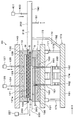
- the peeling apparatus 30 has a processing container 100 that houses a plurality of devices therein.
- a loading / unloading port (not shown) for the processing target wafer W, the support wafer S, and the overlapped wafer T is formed on the side surface of the processing container 100, and an opening / closing shutter (not shown) is provided at the loading / unloading port.
- the processing container 100 in the present embodiment is made of, for example, a stainless steel thin plate and does not seal the inside thereof, but the structure of the processing container 100 is limited to the present embodiment. For example, an airtight container capable of sealing the inside may be used.
- An exhaust port 101 for exhausting the inside of the processing container 100 is formed on the bottom surface of the processing container 100.
- An exhaust pipe 103 communicating with an exhaust device 102 such as a vacuum pump is connected to the exhaust port 101.
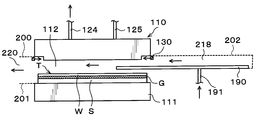
- a first holding unit 110 that holds the wafer W to be processed by suction on the lower surface and a second holding unit 111 that places and holds the support wafer S on the upper surface are provided.
- the first holding unit 110 is provided above the second holding unit 111 and is disposed so as to face the second holding unit 111. That is, in the processing container 100, the peeling process of the superposed wafer T is performed in a state where the processing target wafer W is disposed on the upper side and the supporting wafer S is disposed on the lower side.
- a processing space 112 is formed between the first holding unit 110 and the second holding unit 111 in which the overlapping process of the overlapped wafer T is performed.
- a porous chuck is used for the first holding unit 110.
- the first holding part 110 has a plate-like main body part 120.
- a porous 121 is provided as a porous body in which a plurality of fine holes are formed.
- Porous 121 in contact with the non-bonding surface W N of the processing the wafer W, attracts and holds the object to be processed wafer W.
- the diameter of the holding surface 121 a that holds the processing target wafer W in the porous 121 is smaller than the diameter of the processing target wafer W.
- silicon carbide is used as the porous 121.
- the reason why the diameter of the holding surface 121a of the porous 121 is smaller than the diameter of the wafer W to be processed will be described.
- the superposed wafer T is heated in order to soften the adhesive G.
- the softened adhesive G wraps around the non-joint surface W N at the peripheral edge of the wafer W to be processed (dotted arrow in FIG. 5).
- the diameter of the holding surface 121a of the porous 121 is set to be equal to that of the wafer to be processed W. It is smaller than the diameter.
- a groove 122 is formed between the outer peripheral portion of the main body 120 of the first holding unit 110 and the outer peripheral portion of the wafer W to be processed, as much as the porous 121 is disposed behind.
- a gas circulation space 123 is formed inside the main body 120 and above the porous 121.
- the distribution space 123 is formed so as to cover the porous 121, for example.
- a suction pipe 124 and a gas supply pipe 125 are connected to the circulation space 123.
- the suction tube 124 is connected to a negative pressure generator 126 such as a vacuum pump. Then, the non-joint surface W N of the processing target wafer W is sucked from the suction pipe 124 through the circulation space 123 and the porous 121, and the processing target wafer W is sucked and held by the first holding unit 110.
- the gas supply pipe 125 is connected to an inert gas supply source 127 that supplies, for example, nitrogen gas as an inert gas.
- an inert gas is supplied from the gas supply pipe 125 to the processing space 112 through the circulation space 123 and the porous 121.
- the inert gas is uniformly supplied from the entire surface of the porous 121.
- the suction of the wafer W to be processed from the suction pipe 124 and the supply of the inert gas from the gas supply pipe 125 are switched at a predetermined timing described later.
- the inert gas may be any gas that does not contain oxygen atoms, and is not limited to the nitrogen gas of the present embodiment.
- a heating mechanism 128 that heats the wafer W to be processed is provided inside the main body 120 and above the circulation space 123.
- a heating mechanism 1228 for example, a heater is used.
- a porous ring 130 as a porous part in which a plurality of fine holes are formed is provided on the outer peripheral part of the first holding part 110.
- the porous ring 130 is annularly provided along the outer periphery of the first holding unit 110.
- the porous ring 130 is disposed so as to face the groove 122.
- the porous ring 130 is connected via a gas supply pipe 131 to an inert gas supply source 132 that supplies, for example, nitrogen gas as an inert gas.
- the porous ring 130 can supply an inert gas horizontally with respect to the outer peripheral part of the 1st holding
- silicon carbide is used as the porous ring 130.
- the inert gas may be any gas that does not contain oxygen atoms, and is not limited to the nitrogen gas of the present embodiment.
- a support plate 140 that supports the first holding unit 110 is provided on the upper surface of the first holding unit 110.
- the support plate 140 is supported on the ceiling surface of the processing container 100. Note that the support plate 140 of the present embodiment may be omitted, and the first holding unit 110 may be supported in contact with the ceiling surface of the processing container 100.
- a suction tube 150 for sucking and holding the support wafer S is provided inside the second holding unit 111.
- the suction tube 150 is connected to a negative pressure generator (not shown) such as a vacuum pump.
- a heating mechanism 151 for heating the support wafer S is provided inside the second holding unit 111.
- a heater is used for the heating mechanism 151.
- an elevating mechanism 160 that elevates and lowers the superposed wafer T (or support wafer S) in the processing space 112 is provided.
- the elevating mechanism 160 has, for example, three elevating pins 161 for supporting and lifting the superposed wafer T from below.
- the elevating pin 161 can be moved up and down by the driving unit 162.
- the drive unit 162 includes, for example, a ball screw (not shown) and a motor (not shown) that rotates the ball screw.
- through holes 163 penetrating in the thickness direction through the second holding portion 111 and a support plate 173 described later are formed at, for example, three locations.
- the elevating pins 161 are inserted through the through holes 163 and can protrude from the upper surface of the second holding part 111.
- the moving mechanism 170 that moves the second holding unit 111 and the supporting wafer S in the vertical direction and the horizontal direction is provided below the second holding unit 111.
- the moving mechanism 170 includes a vertical moving unit 171 that moves the second holding unit 111 in the vertical direction and a horizontal moving unit 172 that moves the second holding unit 111 in the horizontal direction.
- the vertical moving unit 171 includes a support plate 173 that supports the lower surface of the second holding unit 111, a drive unit 174 that moves the support plate 173 up and down, and a support member 175 that supports the support plate 173.
- the drive unit 174 has, for example, a ball screw (not shown) and a motor (not shown) that rotates the ball screw.
- the support member 175 is configured to be extendable in the vertical direction, and is provided at, for example, three locations between the support plate 173 and a support body 181 described later.
- the horizontal moving unit 172 includes a rail 180 extending along the X direction (left and right direction in FIG. 3), a support 181 attached to the rail 180, and the support 181 along the rail 180. And a driving unit 182 to be moved.
- the drive unit 182 includes, for example, a ball screw (not shown) and a motor (not shown) that rotates the ball screw.
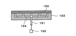
- a porous plate 190 as a porous plate in which a plurality of fine holes are formed is provided on the second holding unit 111 on the positive side in the X direction (left direction in FIG. 3), for example.
- a gas supply pipe 191 that supplies an inert gas to the porous plate 190 is connected to the porous plate 190.
- the porous plate 190 is supported by the support body 181 of the horizontal moving unit 172 via the support member 192. By moving the horizontal moving unit 172, the porous plate 190 can be moved in the horizontal direction. That is, the porous plate 190 moves in the horizontal direction in synchronization with the second holding unit 111.
- the porous plate 190 is Can supply an inert gas to the bonding surface W J of wafer W exposed by the horizontal moving unit 172 moves the second holding portion 111 in a horizontal direction.
- the porous plate 190 for example, silicon carbide is used.
- the porous plate 190 has a flat plate shape that can cover the processing target wafer W in a plan view. Further, at the end in the moving direction of the porous plate 190 when the porous plate 190 is moved by the horizontal moving portion 172, a recessed portion 190a that is recessed in the shape of the wafer W to be processed in plan view is formed. Has been. Specifically, as shown in FIG. 7, the moving direction end of the porous plate 190 is recessed in a semicircular arc shape having substantially the same diameter as the wafer W to be processed, and other than the recessed portion 190 a in the porous plate 190. The location is large enough to cover the wafer W to be processed.
- an end 190b opposite to the end where the recess 190a is formed has a shape protruding in a semicircular arc shape having a larger diameter than the wafer W to be processed. Therefore, the porous plate 190 has a minimum size when covering the processing target wafer W.
- the size of the porous plate 190 is not limited to the present embodiment, and can be arbitrarily set.
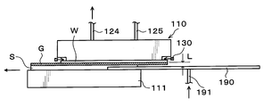
- Porous plate 190 is provided parallel to the bonding surface W J of wafer W as shown in FIGS. Further, the porous plate 190 is formed in a state in which the first holding unit 110 and the second holding unit 111 face each other, that is, in a state where the processing target wafer W and the support wafer S are bonded, as shown in FIG. 190 is disposed such that the recess 190a is in contact with the outer peripheral portion of the wafer W to be processed in plan view.
- the porous plate 190 is adjusted so as to be positioned below the joint surface W J of the processing target wafer W. In other words, between the porous plate 190 and the bonding surface W J of wafer W is spaced in the vertical direction by a predetermined distance. In the present embodiment, the predetermined distance is set to 2 mm.
- a flat plate-like dispersion plate 193 is provided on the lower surface of the porous plate 190 so as to cover the porous plate 190.
- a metal plate such as aluminum or stainless steel is used.
- a gas flow path 194 is formed inside the dispersion plate 193. The gas supply pipe 191 described above is connected to the gas flow path 194 of the dispersion plate 193.
- the end of the gas supply pipe 191 opposite to the dispersion plate 193 side is connected to an inert gas supply source 195 that supplies, for example, nitrogen gas as an inert gas.
- an inert gas supply source 195 that supplies, for example, nitrogen gas as an inert gas.
- the gas flow path 194 of the dispersion plate 174 is provided to be branched into a plurality from the side where the gas supply pipe 191 is connected toward the porous plate 190, and uniformly supplies the inert gas in the plane of the porous plate 190. It is formed to be able to. For this reason, the inert gas supplied from the inert gas supply source 195 is uniformly supplied in-plane to the porous plate 190 via the dispersion plate 193.
- the inert gas may be any gas that does not contain oxygen atoms, and is not limited to the nitrogen gas of the present embodiment.
- the first holding part 110 and the second holding part 111 are provided with a first cover 200 and a second cover 201, respectively.
- the first cover 200 and the second cover 201 are provided so as to cover the processing space 112 between the first holding unit 110 and the second holding unit 111 as described later.
- the first cover 200 is provided with a third cover 202 so as to cover the porous plate 190.
- the first cover 200 has a flat plate portion 210 and a side wall portion 211 as shown in FIGS. 9 and 10.
- the central part of the flat plate part 210 opens along the outer peripheral part of the main body part 120 of the first holding part 110, and the first cover 200 is attached to the first holding part 110 in the opening.
- the side wall portion 211 extends vertically downward from the flat plate 210 and is provided along the moving direction (X direction in the drawing) of the second holding portion 111 and the porous plate 190. In other words, in the first cover 200, both end portions in the moving direction (X direction in the drawing) of the second holding portion 111 and the porous plate 190 are open.
- the side wall 211 is provided so as to cover the porous 121, the groove 122, and the porous ring 130. Note that, as will be described later, a bent portion 212 extending inward in the horizontal direction from the lower end portion 211 is provided at the end portion of the side wall portion 211 on the positive side in the X direction.
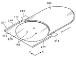
- the second cover 201 has a flat plate portion 213 and a side wall portion 214 as shown in FIG.
- the flat plate portion 213 is attached to the second holding portion 111 so as to cover approximately 2/3 of the outer peripheral portion of the second holding portion 111 on the positive side in the X direction. That is, the flat plate portion 213 is provided at a position where it does not interfere with the porous plate 190 in plan view.
- the bent portion 212 of the first cover 200 described above is disposed at a position where the flat plate portion 213 is not provided on the X direction negative direction side of the second holding portion 111.
- the side wall portion 214 extends vertically upward from the flat plate 220 and is provided along the moving direction (X direction in the drawing) of the second holding portion 111 and the porous plate 190.
- both ends of the second cover 201 in the moving direction (X direction in the drawing) of the second holding unit 111 and the porous plate 190 are open.
- the first cover 200 and the second cover 201 are disposed so as to cover the processing space 112 between the first holding unit 110 and the second holding unit 111 as shown in FIG.
- the first holding part 110 and the second holding part 111 are provided so that the side wall part 211 of the first holding part 110 is positioned outside the side wall part 214 of the second holding part 111.
- the 3rd cover 202 has the ceiling part 215, the side wall part 216, and the bottom face part 217 as shown in FIG.9 and FIG.10.
- the ceiling part 215 and the side wall part 216 are attached to the flat plate part 210 and the side wall part 211 of the first cover 200, respectively.
- the ceiling portion 215 and the bottom surface portion 217 have a planar shape along the outer peripheral portion of the porous plate 190, respectively.
- the side wall part 216 is disposed by connecting the ceiling part 215 and the bottom part 217.
- the third cover 202 is provided so as to cover the porous plate 190, and the standby space 218 of the porous plate 190 is formed inside the third cover 202.
- the end of the porous plate 190 in the moving direction (the negative direction in the X direction in the figure) is open.
- the bottom surface portion 217 has a notch (not shown) to avoid interference with the gas supply pipe 191 and the support member 192.
- the first cover 200, the second cover 201, and the third cover 202 are configured so that the second holding unit 111 and the porous plate 190 can move in the horizontal direction.
- the atmosphere in the space surrounded by the first cover 200, the second cover 201, and the third cover 202 that is, the atmosphere in the processing space 112 and the standby space 218 is the first cover 200.
- the air is exhausted from the opening 220 formed on the side opposite to the third cover 202. That is, the atmosphere in the processing space 112 and the standby space 218 flows toward the X direction negative direction side in the drawing.
- an exhaust device 221 such as a vacuum pump may be provided in the opening 220 in order to positively exhaust the atmosphere in the processing space 112 and the standby space 218.
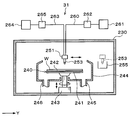
- cleaning apparatus 31 has the process container 230, as shown in FIG.
- a loading / unloading port (not shown) for the wafer W to be processed is formed on the side surface of the processing container 230, and an opening / closing shutter (not shown) is provided at the loading / unloading port.
- a porous chuck 240 that holds and rotates the wafer W to be processed is provided at the center of the processing container 230.
- the porous chuck 240 has a flat plate-like main body 241 and a porous 242 provided on the upper surface side of the main body 241 and formed with a plurality of holes.
- the porous 242 has, for example, substantially the same diameter as the wafer W to be processed, and is in contact with the non-joint surface W N of the wafer W to be processed.
- the porous 242 for example, silicon carbide is used.
- a suction tube (not shown) is connected to the porous 242, and the non-bonded surface W N of the wafer to be processed W is sucked from the suction tube through the porous 242, so that the wafer to be processed W is placed on the porous chuck 240. Can be adsorbed and retained.
- a chuck driving unit 243 provided with a motor or the like is provided below the porous chuck 240.
- the porous chuck 240 can be rotated at a predetermined speed by the chuck driving unit 243.
- the chuck driving unit 243 is provided with an elevating drive source such as a cylinder, and the porous chuck 240 is movable up and down.
- a cup 244 that receives and collects the liquid scattered or dropped from the wafer W to be processed.
- a discharge pipe 245 for discharging the collected liquid
- an exhaust pipe 246 for evacuating and exhausting the atmosphere in the cup 244.
- a rail 250 extending along the Y direction is formed on the negative side of the cup 244 in the X direction (downward direction in FIG. 14).
- the rail 250 is formed from the outside of the cup 244 on the Y direction negative direction (left direction in FIG. 14) side to the outside on the Y direction positive direction (right direction in FIG. 14) side.
- An arm 251 is attached to the rail 250.
- the arm 251 supports a cleaning liquid nozzle 253 for supplying a cleaning liquid, for example, an organic solvent, to the wafer W to be processed.
- the arm 251 is movable on the rail 250 by a nozzle driving unit 254 shown in FIG.
- the cleaning liquid nozzle 253 can move from the standby part 255 installed outside the Y direction positive direction side of the cup 244 to above the center of the wafer W to be processed in the cup 244, and further on the wafer W to be processed. Can be moved in the radial direction of the wafer W to be processed.
- the arm 251 can be moved up and down by the nozzle driving unit 254, and the height of the cleaning liquid nozzle 253 can be adjusted.
- a two-fluid nozzle is used as the cleaning liquid nozzle 253.
- a supply pipe 260 that supplies the cleaning liquid to the cleaning liquid nozzle 253 is connected to the cleaning liquid nozzle 253.
- the supply pipe 260 communicates with a cleaning liquid supply source 261 that stores the cleaning liquid therein.
- the supply pipe 260 is provided with a supply device group 262 including a valve for controlling the flow of the cleaning liquid, a flow rate adjusting unit, and the like.
- a supply pipe 263 that supplies, for example, nitrogen gas as an inert gas to the cleaning liquid nozzle 253 is connected to the cleaning liquid nozzle 253.
- the supply pipe 263 communicates with an inert gas supply source 264 that stores an inert gas therein.
- the supply pipe 263 is provided with a supply device group 265 including a valve for controlling the flow of the inert gas, a flow rate adjusting unit, and the like.
- the cleaning liquid and the inert gas are mixed in the cleaning liquid nozzle 253 and supplied to the wafer W to be processed from the cleaning liquid nozzle 253.
- a mixture of a cleaning liquid and an inert gas may be simply referred to as “cleaning liquid”.
- lifting pins for supporting the wafer W to be processed from below and lifting it may be provided below the porous chuck 240.
- the elevating pins can pass through a through hole (not shown) formed in the porous chuck 240 and protrude from the upper surface of the porous chuck 240. Then, instead of moving the porous chuck 240 up and down, the lift pins are moved up and down, and the wafer W to be processed is transferred to and from the porous chuck 240.
- the configuration of the second cleaning device 33 is substantially the same as the configuration of the first cleaning device 31 described above.
- the second cleaning device 33 is provided with a spin chuck 270 instead of the porous chuck 240 of the first cleaning device 31 as shown in FIG.
- the spin chuck 270 has a horizontal upper surface, and a suction port (not shown) for sucking, for example, the support wafer S is provided on the upper surface.
- the support wafer S can be sucked and held on the spin chuck 270 by suction from the suction port. Since the other structure of the 2nd washing
- cleaning apparatus 33 is the same as that of the structure of the 1st washing
- a back rinse nozzle (not shown) for injecting the cleaning liquid toward the back surface of the support wafer S, that is, the non-bonding surface SN is provided. Also good.
- the non-bonding surface SN of the support wafer S and the outer peripheral portion of the support wafer S are cleaned by the cleaning liquid sprayed from the back rinse nozzle.
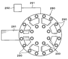
- the second transfer device 32 has a Bernoulli chuck 280 that holds the wafer W to be processed as shown in FIG. Bernoulli chuck 280 is supported by support arm 281.
- the support arm 281 is supported by the first drive unit 282.
- the first drive unit 282 allows the support arm 281 to rotate around the horizontal axis and extend and contract in the horizontal direction.
- a second driving unit 283 is provided below the first driving unit 282. By this second drive unit 283, the first drive unit 282 can rotate about the vertical axis and can be moved up and down in the vertical direction.
- the Bernoulli chuck 280 described above is provided with a plurality of gas outlets 290 for injecting, for example, nitrogen gas as an inert gas.
- the plurality of gas ejection ports 290 are arranged on the concentric circles of the Bernoulli chuck 280 and at equal intervals on the double concentric circles.
- An inert gas supply source 292 that supplies an inert gas is connected to each gas outlet 290 via a gas supply pipe 291.
- the Bernoulli chuck 280 can float the wafer W to be processed by ejecting an inert gas, and can hold the wafer W to be sucked and suspended in a non-contact state.
- positioning of the gas jet outlet 290 are not limited to this Embodiment, It can set arbitrarily.
- the 3rd conveying apparatus 41 has the structure similar to the 2nd conveying apparatus 32 mentioned above, description is abbreviate
- the second drive unit 283 of the third transport device 41 is attached to the transport path 40 shown in FIG. 1, and the third transport device 41 is movable on the transport path 40.
- the control unit 300 is a computer, for example, and has a program storage unit (not shown).
- the program storage unit stores a program for controlling processing of the processing target wafer W, the supporting wafer S, and the overlapped wafer T in the peeling system 1.
- the program storage unit also stores a program for controlling the operation of drive systems such as the above-described various processing apparatuses and transport apparatuses to realize a peeling process described later in the peeling system 1.
- the program is recorded on a computer-readable storage medium H such as a computer-readable hard disk (HD), a flexible disk (FD), a compact disk (CD), a magnetic optical desk (MO), or a memory card. May have been installed in the control unit 300 from the storage medium H.
- FIG. 18 is a flowchart showing an example of main steps of the peeling process.
- a cassette C T accommodating a plurality of bonded wafer T, an empty cassette C W, and an empty cassette C S is placed on the predetermined cassette mounting plate 11 of the carry-out station 2.
- the superposed wafer T in the cassette CT is taken out by the first transfer device 20 and transferred to the peeling device 30 of the peeling processing station 3.
- the superposed wafer T is transported in a state where the processing target wafer W is disposed on the upper side and the support wafer S is disposed on the lower side.
- the superposed wafer T carried into the peeling device 30 is transferred to the lift pins 161 that have been lifted and waited in advance as shown in FIGS. Thereafter, the second holding unit 111 is raised to a predetermined position by the moving mechanism 170, and the overlapped wafer T is held by the lift pins 161 in the processing space 112 from the gas supply pipe 125 and the gas supply pipe 191. An inert gas is supplied into the processing space 112 (step A1 in FIG. 18).
- the second holding unit 111 is disposed, for example, at a position where the vertical distance of the processing space 112 is about 10 mm.
- the overlapped wafer T is held by the lift pins 161 in the processing space 112 and is disposed at a position where it does not come in contact with either the first holding unit 110 or the second holding unit 111. For this reason, the superposed wafer T is not heated by the heating mechanisms 128 and 151.
- the inert gas is supplied from the gas supply pipe 125 and the gas supply pipe 191 with the superposed wafer T held by the elevating pins 161 in this way.
- the inert gas supplied from the gas supply pipe 125 flows through the processing space 112, that is, both the upper and lower sides of the superposed wafer T, and is exhausted from the opening 220. Further, the inert gas supplied from the gas supply pipe 191 through the porous plate 190 is sequentially circulated in the standby space 218 and the processing space 112 and is exhausted from the opening 220. Thus, the atmosphere in the processing space 112 from which the superposed wafer T is peeled is replaced with the inert gas, and the atmosphere is maintained at a predetermined low oxygen concentration of ppm level.
- step A1 since the volume of the processing space 112 is reduced by raising the second holding unit 111, the atmosphere of the processing space 112 reaches a predetermined low oxygen concentration in a short time. Further, without bonded wafer T is heated, moreover since the inert gas is supplied into the processing space 112, it is possible to suppress the oxidation of the non-bonding surface W N of the processed wafers W.
- the elevating pins 161 are lowered, and the overlapped wafer T is placed on the second holding unit 111. Subsequently, the superposed wafer T is sucked from the suction tube 150, and the non-bonding surface SN of the support wafer S is sucked and held by the second holding unit 111 (step A2 in FIG. 19). At this time, the supply of the inert gas from the gas supply pipe 125 and the gas supply pipe 191 to the processing space 112 is continued.
- the second holding unit 111 may be raised by the moving mechanism 170.
- the supply of the inert gas from the gas supply pipe 125 is stopped, and the suction from the suction pipe 124 is started. Further, an inert gas is supplied from the porous ring 130 to the outer periphery of the first holding unit 110. Subsequently, by increasing the second holding portion 111 by the moving mechanism 170 as shown in FIGS. 23 and 24, holds adsorb non-bonding surface W N of the wafer W by the first holding portion 110 (FIG. 19 step A2).
- the inert gas is supplied from the porous ring 130 to the outer periphery of the first holding unit 110 as described above.
- the inert gas is supplied from the porous ring 130 in which a plurality of holes are formed, the flow rate of the inert gas is suppressed.
- only inert gas is supplied to the outer peripheral part of the 1st holding
- the inert gas is supplied to the groove 122 between the first holding unit 110 and the wafer W to be processed, the inside of the groove 122 is an inert gas atmosphere.
- the superposed wafer T is heated to a predetermined temperature, for example, 200 ° C. by the heating mechanisms 128 and 151. Thereby, the adhesive G in the superposed wafer T is softened.
- the supply of the inert gas from the gas supply pipe 191 is also continued. That is, the inert gas is supplied from the upper surface of the porous plate 190 via the gas supply pipe 191 and the dispersion plate 193.
- the flow rate of the inert gas supplied from the porous plate 190 can be suppressed by supplying the inert gas through the porous plate 190 in which a plurality of fine holes are formed. For this reason, ambient air is not involved when supplying the inert gas.
- an inert gas atmosphere that does not contain air can be formed on the upper surface side of the porous plate 190.
- a gas flow path 194 that is branched into a plurality toward the porous plate 190 is formed inside the dispersion plate 193, an inert gas is uniformly supplied from the entire upper surface side of the porous plate 190. Is done.
- the second holding unit 111 and the support wafer S are moved in the horizontal direction by the moving mechanism 170 as shown in FIG.
- the porous plate 190 is supported by the horizontal movement unit 172 by the support body 181
- the porous plate 190 moves in the horizontal direction in synchronization with the second holding unit 111 in accordance with the operation of the horizontal movement unit 172.
- the porous plate 190 is wafer W It moves in the horizontal direction without interfering with the bonding surface W J of. Therefore, the bonding surface W J of wafer W exposed by this movement, a state of facing apart porous plate 190 and the distance L. And during this time, the bonding surface W J of wafer W inert gas is supplied from the porous plate 190.
- the second holding unit 111 is moved in the horizontal direction while the supply of the inert gas from the porous plate 190 is continued, and the wafer to be processed held by the first holding unit 110 as shown in FIG. W and the support wafer S held by the second holding unit 111 are separated (step A3 in FIG. 19).
- the porous plate 190 is formed to a size capable of covering the wafer W in a plan view, of continuing the porous plate 190 to the bonding surface W J of wafer W that peeling is completed not Active gas is supplied.
- the processing target wafer W peeled by the peeling device 30 is transferred from the first holding unit 110 to the Bernoulli chuck 280 of the second transfer device 32 as shown in FIG.
- the support arm 281 is extended, and the Bernoulli chuck 280 is disposed below the wafer W to be processed held by the first holding unit 110.
- the Bernoulli chuck 280 is raised, and the suction of the wafer W to be processed from the suction tube 124 in the first holding unit 110 is stopped.
- the processing target wafer W is delivered from the first holding unit 110 to the Bernoulli chuck 280.
- the Bernoulli chuck 280 is lowered to a predetermined position.
- the wafer W to be processed is held in a non-contact state by the Bernoulli chuck 280. Therefore, wafer W is held without device on the bonding surface W J of wafer W suffers damage.
- the second holding unit 111 moves to a position facing the first holding unit 110.
- an inert gas to the bonding surface W J of wafer W from the Bernoulli chuck 280 is supplied (step A4 in FIG. 19).
- the wafer W to be processed is cooled to a predetermined temperature, for example, 100 ° C. to 150 ° C. or less.
- the supply of the inert gas from the gas supply pipe 125 is stopped.
- the processing target wafer W cooled to a predetermined temperature is transferred to the first cleaning device 31 by the second transfer device 32 as shown in FIG. 29 while being held by the porous chuck 280.
- the support arm 281 is rotated to move the Bernoulli chuck 280 above the porous chuck 240 of the first cleaning device 31 and the Bernoulli chuck 280 is inverted to reverse the wafer W to be processed. Turn down.
- the porous chuck 240 is raised to a position higher than the cup 244 and kept waiting.
- the wafer W to be processed is delivered from the Bernoulli chuck 280 to the porous chuck 240 and held by suction.
- the porous chuck 240 When the wafer W to be processed is sucked and held on the porous chuck 240 in this way, the porous chuck 240 is lowered to a predetermined position. Subsequently, the arm 251 moves the cleaning liquid nozzle 253 of the standby unit 255 to above the center of the wafer W to be processed. Thereafter, while rotating the wafer W by the porous chuck 240, and supplies the cleaning liquid from the cleaning liquid nozzle 253 to the bonding surface W J of wafer W. Supplied cleaning liquid is diffused over the entire surface of the bonding surface W J of wafer W by the centrifugal force, the bonding surface W J of the wafer W is cleaned (step A5 in FIG. 19).
- the plurality of superposed wafers T carried into the carry-in / out station 2 have been inspected in advance, and the superposed wafer T including the normal target wafer W and the defective target wafer W are arranged.
- the superposed wafer T is discriminated.
- the transfer of the wafer W to be processed by the third transfer device 41 is substantially the same as the transfer of the wafer W to be processed by the second transfer device 32 described above, and thus the description thereof is omitted.
- Step A6 in FIG. 19 whether the adhesive residue G at the joint surface W J of wafer W is inspected.
- the wafer W to be processed is transferred to the bonding surface cleaning unit 8a of the post-inspection cleaning device 8 by the third transfer device 41, and the bonding surface is cleaned by the bonding surface cleaning unit 8a.
- W J is cleaned (step A7 in FIG. 19).
- bonding surface W J is cleaned wafer W is transported to the inversion portion 8c by the third transporting device 41 is reversed in the vertical direction in reversing unit 8c.
- the residue of the adhesive agent G is not confirmed, the to-be-processed wafer W is reversed by the inversion part 8c, without being conveyed to the joining surface washing
- wafer W being inverted is conveyed to the inspection device 7 again by the third transporting device 41, the inspection of the non-bonding surface W N is performed (step A9 in FIG. 19).
- the wafer W to be processed is transferred to the non-bonding surface cleaning unit 8c by the third transfer device 41, and the non-bonding surface W N is cleaned. (Step A10 in FIG. 19).
- the cleaned wafer W to be processed is transferred to the post-processing station 4 by the third transfer device 41. If no residue of the adhesive G is confirmed by the inspection device 7, the wafer W to be processed is transferred to the post-processing station 4 as it is without being transferred to the non-bonding surface cleaning unit 8b.
- predetermined post-processing is performed on the processing target wafer W in the post-processing station 4 (step A11 in FIG. 19).
- the processing target wafer W is commercialized.
- wafer W with a peel defects from bonded wafer T including a defect is conveyed to the station 2 loading and unloading by the first transfer device 20. Thereafter, the processing target wafer W having a defect is unloaded from the loading / unloading station 2 and collected (step A12 in FIG. 19).
- the support wafer S peeled off by the peeling device 30 is transferred to the second cleaning device 33 by the first transfer device 20. Then, in the second cleaning device 33, bonding surface S J of the support wafer S is cleaned (step A13 in FIG. 19). Note that the cleaning of the support wafer S in the second cleaning device 33 is the same as the cleaning of the wafer W to be processed in the first cleaning device 31 described above, and thus the description thereof is omitted.
- the support wafer S which joint surface S J is cleaned is conveyed to station 2 loading and unloading by the first transfer device 20. Thereafter, the support wafer S is unloaded from the loading / unloading station 2 and collected (step A14 in FIG. 19). In this way, a series of separation processing of the processing target wafer W and the supporting wafer S is completed.
- the outer periphery of the first holding unit 110 from the porous ring 130 in which a plurality of holes are formed.
- An inert gas is supplied to the section.
- the adhesive G heated in the process A3 is not bonded to the peripheral portion of the wafer W to be processed. Even when it wraps around W N , the adhesive G remains in the groove 122 and does not adhere to the porous 121. For this reason, it is possible to prevent the porous 121 and the wafer to be processed W from being fixed, and to appropriately transfer the wafer to be processed W from the first holding unit 110 to the Bernoulli chuck 280 in step A4.
- the inert gas from the porous ring 130 can be horizontally supplied to the groove 122 formed between the first holding unit 110 and the wafer W to be processed in this way, the inside of the groove 122 is inactive. A gas atmosphere can be obtained. Therefore, only the inert gas can be reliably supplied by the gap between the holding surface 121a of the first holding unit 110 and the non-bonding surface W N of the wafer to be processed, and the heat-treated wafer W to be processed can be supplied. the oxidation of the non-bonding surface W N can be further suppressed.
- Step A1 an inert gas is supplied from the gas supply pipe 125 to the processing space 112, and an inert gas is also supplied from the gas supply pipe 191 into the processing space 112 via the standby space 218.
- the processing space 112 is covered with the first cover 200 and the second cover 201, and the standby space 218 is covered with the third cover 202, and the inside of the processing space 112 and the standby space 218 is directed to the opening 220.
- An inert gas stream is formed. For this reason, the inside of the processing space 112 can be filled with an inert gas, and the atmosphere in the processing space 112 can be maintained at a low oxygen concentration.
- step A1 it is possible to suppress the oxidation of the non-bonding surface W N of the wafer W in step A1. Also in the subsequent step A3, it is possible to lower the oxygen concentration the atmosphere in the processing space 112, it is possible to suppress the oxidation of the bonding surface W J of the processing target wafer W.
- the bonding surface W J of wafer W exposed by moving the second holding portion 111 in a horizontal direction by a moving mechanism 170 since the inert gas is supplied from the porous plate 190, peeling the bonding surface W J of wafer W exposed by can be an atmosphere of inert gas. Thus, it is possible to suppress the oxidation of the bonding surface W J of the heated treated wafer W.
- the porous plate 190 because it is a size large enough to cover the wafer W, it is possible to supply the inert gas to the entire surface of the bonding surface W J of wafer W peeled. For this reason, oxidation can be suppressed over the entire surface of the wafer W to be processed.
- the porous plate 190 is covered in plan view. It can be arranged at a position in contact with the processing wafer W. Therefore, the bonding surface W J of wafer W exposed by moving the moving mechanism 170, it is possible to supply the inert gas immediately.
- the bonding surface W J of wafer W is crescent as shown in FIG. 30 It is exposed in a shape (range shown by hatching in FIG. 30).
- a recess 190a is formed in the porous plate 190, and the porous plate 190 is disposed so that the recess 190a contacts the wafer W to be processed in a plan view, so that the entire crescent-shaped exposed portion is covered with the porous plate 190. Can be covered. Therefore, it supplies an inert gas immediately on the entire surface of the exposed bonding surface W J.
- the depression 190a is in contact with the outer periphery of the wafer W to be processed in a plan view, and the diameter of the arc of the depression 190a and the diameter of the wafer W to be processed are in contact with each other over the entire circumference of the depression 190a.
- the porous plate 190 It means that the hollow part 190a of the porous plate 190 and the outer peripheral part of the wafer W to be processed are close to each other in a plan view to the extent that it is covered with the inert gas atmosphere above.
- step A4 to wafer W held by the Bernoulli chuck 280, with an inert gas to the bonding surface W J from the Bernoulli chuck 280 is supplied to the non-bonding surface W N from the gas supply pipe 125 An inert gas is supplied. Since wafer W is properly cooled to a predetermined temperature, it never thereafter oxidized in joint surface W J and a non-bonding surface W N of the wafer W proceeds. Moreover, what is used to cool the wafer W is because an inert gas may also during cooling to prevent oxidation of the bonding surface W J and a non-bonding surface W N of the wafer W.
- the porous ring 130 horizontally supplies the inert gas from the plurality of holes, but as shown in FIG. 31, the inert gas is supplied obliquely upward from the plurality of holes. Also good.
- the inert gas supplied from the porous ring 130 to the groove portion 122 collides with the bottom surface of the main body portion 120 or the side surface of the porous 121 and convects and diffuses in the groove portion 122. And the inside of the groove part 122 is filled with an inert gas.
- the inert gas can be supplied to the gap between the holding surface 121a of the first holding unit 110 and the non-bonding surface W N of the wafer to be processed, and the non-bonding of the heat-treated wafer W to be processed can be performed. It is possible to suppress the oxidation of the surface W N.
- the ion gas supply pipe 400 may be connected to the third cover 202 as shown in FIG.
- the ion gas supply pipe 400 is provided with an ionizer 401 that ionizes, for example, nitrogen gas as an inert gas. Then, for example, in steps A1 to A3, the ionized inert gas is supplied from the ion gas supply pipe 400 into the standby space 218, and sequentially flows through the standby space 218 and the processing space 112 to be exhausted from the opening 220.
- the inert gas may be any gas that does not contain oxygen atoms, and is not limited to the nitrogen gas of the present embodiment.
- the peeling charge of the wafer to be processed W can be neutralized by the ionized inert gas. That is, damage to the processing target wafer W due to static electricity can be prevented.
- the inert gas positively ionized into the standby space 218 from the ion gas supply pipe 400 the flow of the inert gas toward the opening 220 in the standby space 218 and the processing space 112 is more sure. Can be formed. For this reason, the oxidation of the surface of the processing target wafer W in the processing space 112 can be further suppressed.
- the ion gas supply pipe 400 is connected to the ceiling 215 of the third cover 202.
- the ion gas supply pipe 400 is an end of the third cover 202 opposite to the opening,
- the ion gas supply pipe 400 may be connected to the side wall portion 216 of the third cover 202.
- silicon carbide is used for the porous ring 130 and the porous plate 190, respectively, but these materials are not limited to the present embodiment.
- Teflon (registered trademark) or the like may be used as long as a plurality of fine holes that do not entrain the surrounding air when the inert gas is supplied from the porous ring 130 and the porous plate 190 are formed.
- the porous plate 190 a distance L between the joint surface W J of wafer W had a 2 mm, the distance L is long in the range of 0.5 mm ⁇ 4 mm, wafer W appropriately supplying an inert gas to the bonding surface W J, it is possible to suitably suppress the progress of rapid oxidation.
- the porous plate 190 had been placed parallel to the bonding surface W J of wafer W, the porous plate 190 is always parallel to the bonding surface W J of wafer W there need not, if the distance L between the porous plate 190 and the bonding surface W J is kept between 0.5 mm ⁇ 4 mm, the porous plate 190 is provided inclined with respect to joint surface W J May be.
- the inert gas supply sources 127, 132, and 195 are provided separately, but a common inert gas supply source may be provided.
- the second holding unit 111 is moved in the horizontal direction relative to the first holding unit 110.
- the holding portion 111 may be moved 100 ⁇ m in the vertical direction.
- the moving distance of the second holding unit 111 in the horizontal direction is 300 mm
- the thickness of the adhesive G in the superposed wafer T is, for example, 30 ⁇ m to 40 ⁇ m
- the bonding surface of the wafer W to be processed height of W J to form devices (bump) is 20 ⁇ m for example.
- the distance between the device on the processing target wafer W and the support wafer S is very small.
- the ratio of the vertical movement distance and the horizontal movement distance of the second holding unit 111 is appropriately set based on the height of the device (bump) on the wafer W to be processed.
- the present invention is not limited to the embodiment.
- first holding unit 110 may be moved instead of the second holding unit 111. In such a case, the first holding unit 110 may be moved in the vertical direction and the horizontal direction. Alternatively, both the first holding unit 110 and the second holding unit 111 may be moved in the vertical direction and the horizontal direction.
- the porous plate 190 is horizontally oriented with respect to the wafer W to be processed held by the first holding unit 110, that is, the object to which the inert gas is supplied, when any of the holding units 110 and 111 is moved.
- the moving method and the supporting method can be arbitrarily set as long as they are configured to move relative to each other.
- the porous plate 190 when the first holding unit 110 is moved in the horizontal direction, the porous plate 190 may be supported on the ceiling surface of the processing container 100 or may be supported on the bottom surface of the processing container 100. In either case, the processed wafer W is, if moving above the porous plate 190 in the horizontal direction in a state in which the porous plate 190 and the predetermined distance L spaced, the joining surfaces W J of wafer W exposed It can be an atmosphere of an inert gas.
- Step A3 instead of moving the second holding unit 111 in the vertical direction and the horizontal direction, the second holding unit 111 is moved only in the horizontal direction, and the moving speed of the second holding unit 111 is changed. May be changed. Specifically, the moving speed at the start of moving the second holding unit 111 may be reduced, and then the moving speed may be gradually accelerated. That is, when the second holding unit 111 starts to move, the bonding area between the processing target wafer W and the support wafer S is large, and the device on the processing target wafer W is easily affected by the adhesive G. The moving speed of the second holding unit 111 is lowered.
- the device on the wafer to be processed W becomes less susceptible to the adhesive G, so that the moving speed of the second holding unit 111 is gradually increased. To accelerate. Even in such a case, contact between the device and the support wafer S can be avoided, and damage to the device can be suppressed.
- the wafer to be processed W and the support wafer S are separated in a state where the wafer to be processed W is arranged on the upper side and the support wafer S is arranged on the lower side.
- the vertical arrangement of the wafer W and the support wafer S may be reversed.
- a heating unit for example, a heater for heating the inert gas supplied to the processing space 112 and the standby space 218 may be provided.
- the inert gas supplied from the gas supply pipes 125 and 191 may be heated in advance.
- an inert gas having substantially the same temperature (for example, 200 ° C.) as the first holding unit 111 and the second holding unit 112 may be supplied to the processing space 112 and the standby space 218.
- the porous plate 190 is provided with a heater 450 on the lower surface of the dispersion plate 193 as shown in FIG.
- the heater 450 is a film-like heater.
- a pressing plate 451 for pressing the heater 450 is disposed below the heater 450, and the heater 450 is sandwiched between the dispersion plate 193 and the pressing plate 451.
- the porous plate 190, the dispersion plate 193, and the pressing plate 451 are preferably made of materials that have substantially the same amount of thermal expansion during heating.
- the first holding unit 110 is also provided with a heater as a heating unit, the heater is the same as the heater 450 described above, and a description thereof will be omitted.
- a monitoring means 500 for monitoring a blockage of a plurality of holes in the porous plate 190 may be provided.
- the monitoring unit 500 includes a plurality of through holes 501 provided in the porous plate 190, a pipe 502 having one end connected to the through hole 501, and a pressure gauge 503 arranged in the middle of the pipe 502. Note that the other end of the pipe 502 is open.
- the diameter of the through hole 501 is preferably small, for example, 1 mm.
- the through holes 501 are provided at predetermined intervals on a line similar to the end of the recess 190a, and are arranged in a plurality of rows.
- the inner surface 504 of the through hole 501 is sealed by a coating process or the like.
- a pressure gauge 503 is provided to detect the pressure, and when the pressure becomes smaller than a predetermined value, it is considered that a hole clogging has occurred in the porous plate 190 around the through hole 501; Make a warning. Then, the peeling process is stopped and the cleaning operation is performed. In this way, it is possible to prevent clogging of the porous plate 190 and to always inject the inert gas from the porous plate 190 uniformly.
- the pressure difference with the room is monitored by the pressure gauge 503, but a suction pump (not shown) may be connected to the other end of the pipe 502 and the absolute pressure may be monitored by the pressure gauge 503. .
- the present invention is not limited to such examples. It is obvious for those skilled in the art that various changes or modifications can be conceived within the scope of the idea described in the claims, and these naturally belong to the technical scope of the present invention. It is understood.
- the present invention is not limited to this example and can take various forms.
- the present invention can also be applied to a case where the substrate is another substrate such as an FPD (flat panel display) other than a wafer or a mask reticle for a photomask.
- FPD flat panel display
Landscapes
- Engineering & Computer Science (AREA)
- Mechanical Engineering (AREA)
- Container, Conveyance, Adherence, Positioning, Of Wafer (AREA)
Abstract
L'invention porte sur un dispositif de séparation qui sépare un substrat composite, qui comprend un substrat traité lié à un substrat de support par un adhésif, en ledit substrat traité et ledit substrat de support. Ledit dispositif de séparation présente les éléments suivants : une première partie de support qui supporte le substrat traité et comporte un mécanisme de chauffage qui chauffe ledit substrat ; une seconde partie de support qui supporte le substrat de support et comporte un mécanisme de chauffage qui chauffe ledit substrat ; un mécanisme de déplacement qui déplace au moins la première ou la seconde partie de support horizontalement par rapport à l'autre ; et une partie poreuse qui est disposée de façon à former un anneau autour du bord externe de la première partie de support, contient une pluralité de trous, et fournit un gaz inerte au bord externe de la première partie de support supportant le substrat traité.
Priority Applications (1)
| Application Number | Priority Date | Filing Date | Title |
|---|---|---|---|
| US14/009,850 US9827756B2 (en) | 2011-04-12 | 2012-03-16 | Separation apparatus, separation system, and separation method |
Applications Claiming Priority (2)
| Application Number | Priority Date | Filing Date | Title |
|---|---|---|---|
| JP2011-087915 | 2011-04-12 | ||
| JP2011087915 | 2011-04-12 |
Publications (1)
| Publication Number | Publication Date |
|---|---|
| WO2012140987A1 true WO2012140987A1 (fr) | 2012-10-18 |
Family
ID=47009169
Family Applications (1)
| Application Number | Title | Priority Date | Filing Date |
|---|---|---|---|
| PCT/JP2012/056864 Ceased WO2012140987A1 (fr) | 2011-04-12 | 2012-03-16 | Dispositif de séparation, système de séparation et procédé de séparation |
Country Status (4)
| Country | Link |
|---|---|
| US (1) | US9827756B2 (fr) |
| JP (1) | JP5740583B2 (fr) |
| TW (1) | TWI527141B (fr) |
| WO (1) | WO2012140987A1 (fr) |
Cited By (3)
| Publication number | Priority date | Publication date | Assignee | Title |
|---|---|---|---|---|
| CN103846646A (zh) * | 2012-12-07 | 2014-06-11 | 富泰华工业(深圳)有限公司 | 拆卸装置 |
| CN105428468A (zh) * | 2015-12-31 | 2016-03-23 | 苏州博阳能源设备有限公司 | 一种硅片插片装置 |
| EP3866184A1 (fr) * | 2012-11-30 | 2021-08-18 | Nikon Corporation | Système de support, appareil d'exposition et procédé d'acheminement |
Families Citing this family (12)
| Publication number | Priority date | Publication date | Assignee | Title |
|---|---|---|---|---|
| JP6184717B2 (ja) * | 2013-03-28 | 2017-08-23 | 株式会社ディスコ | ウェーハ貼着装置 |
| JP6466217B2 (ja) * | 2014-04-10 | 2019-02-06 | 東京エレクトロン株式会社 | 剥離装置及び剥離システム |
| JP6195803B2 (ja) * | 2014-05-02 | 2017-09-13 | 東京エレクトロン株式会社 | 基板処理装置、基板処理方法および記憶媒体 |
| KR20160057966A (ko) | 2014-11-14 | 2016-05-24 | 가부시끼가이샤 도시바 | 처리 장치, 노즐 및 다이싱 장치 |
| US9627259B2 (en) | 2014-11-14 | 2017-04-18 | Kabushiki Kaisha Toshiba | Device manufacturing method and device |
| DE102014118017A1 (de) | 2014-12-05 | 2016-06-09 | Ev Group E. Thallner Gmbh | Substratstapelhalterung, Container und Verfahren zur Trennung eines Substratstapels |
| JP6305355B2 (ja) | 2015-01-28 | 2018-04-04 | 株式会社東芝 | デバイスの製造方法 |
| JP6545511B2 (ja) | 2015-04-10 | 2019-07-17 | 株式会社東芝 | 処理装置 |
| CN106710442B (zh) * | 2015-10-21 | 2021-01-22 | 京东方科技集团股份有限公司 | 背光源分离设备 |
| KR102505213B1 (ko) * | 2017-12-08 | 2023-03-03 | 삼성전자주식회사 | 분리용 전자 장치 및 이의 공정 방법 |
| NL2023097B1 (en) * | 2019-05-09 | 2020-11-30 | Suss Microtec Lithography Gmbh | Stamp replication device and method for producing a holding means for a stamp replication device as well as a stamp |
| CN114476681A (zh) * | 2022-03-09 | 2022-05-13 | 河北泰晶新材料科技有限公司 | 一种物料输送系统、物料输送方法及存储介质 |
Citations (3)
| Publication number | Priority date | Publication date | Assignee | Title |
|---|---|---|---|---|
| JP2004063645A (ja) * | 2002-07-26 | 2004-02-26 | Enzan Seisakusho:Kk | 半導体ウェハの保護部材剥離装置 |
| JP2008277552A (ja) * | 2007-04-27 | 2008-11-13 | Shin Etsu Chem Co Ltd | 貼り合わせ基板の製造方法 |
| JP2010010207A (ja) * | 2008-06-24 | 2010-01-14 | Tokyo Ohka Kogyo Co Ltd | 剥離装置および剥離方法 |
Family Cites Families (18)
| Publication number | Priority date | Publication date | Assignee | Title |
|---|---|---|---|---|
| KR0165467B1 (ko) | 1995-10-31 | 1999-02-01 | 김광호 | 웨이퍼 디본더 및 이를 이용한 웨이퍼 디본딩법 |
| JP3599322B2 (ja) * | 1999-07-28 | 2004-12-08 | 東京エレクトロン株式会社 | 基板処理装置及び基板処理方法 |
| JP2002100595A (ja) * | 2000-07-21 | 2002-04-05 | Enya Systems Ltd | ウエ−ハ剥離装置及び方法並びにこれを用いたウエ−ハ処理装置 |
| JP2003174077A (ja) * | 2001-12-04 | 2003-06-20 | Lintec Corp | 吸着保持装置 |
| JP4130167B2 (ja) * | 2003-10-06 | 2008-08-06 | 日東電工株式会社 | 半導体ウエハの剥離方法 |
| JP4798754B2 (ja) | 2005-05-24 | 2011-10-19 | リンテック株式会社 | エネルギー線照射装置とその方法 |
| JP4666496B2 (ja) * | 2005-12-07 | 2011-04-06 | 大日本スクリーン製造株式会社 | 基板熱処理装置 |
| JP4670677B2 (ja) * | 2006-02-17 | 2011-04-13 | 東京エレクトロン株式会社 | 加熱装置、加熱方法、塗布装置及び記憶媒体 |
| US20080200011A1 (en) * | 2006-10-06 | 2008-08-21 | Pillalamarri Sunil K | High-temperature, spin-on, bonding compositions for temporary wafer bonding using sliding approach |
| JP2008153337A (ja) * | 2006-12-15 | 2008-07-03 | Tokyo Electron Ltd | 貼り合せ基板の分離方法、貼り合せ基板の分離装置及びプログラムを記録したコンピュータ読み取り可能な記録媒体 |
| JP5487560B2 (ja) * | 2008-05-28 | 2014-05-07 | 富士通株式会社 | 基板処理装置及び基板処理方法 |
| US8443863B2 (en) * | 2008-10-23 | 2013-05-21 | Corning Incorporated | High temperature sheet handling system and methods |
| JP2010153483A (ja) * | 2008-12-24 | 2010-07-08 | Toyota Motor Corp | 成膜装置、及び、成膜方法 |
| EP2660851B1 (fr) * | 2009-03-18 | 2020-10-14 | EV Group GmbH | Dispositif et procédé de séparation d'une tranche de silicium à partir d'un support |
| US7989266B2 (en) * | 2009-06-18 | 2011-08-02 | Aptina Imaging Corporation | Methods for separating individual semiconductor devices from a carrier |
| JP5412214B2 (ja) * | 2009-08-31 | 2014-02-12 | 日東電工株式会社 | 保護テープ剥離方法およびその装置 |
| KR20120132472A (ko) * | 2009-12-23 | 2012-12-05 | 수스 마이크로텍 리소그라피 게엠바하 | 자동 열 슬라이드 디본더 |
| US8758553B2 (en) * | 2010-10-05 | 2014-06-24 | Skyworks Solutions, Inc. | Fixtures and methods for unbonding wafers by shear force |
-
2012
- 2012-03-16 WO PCT/JP2012/056864 patent/WO2012140987A1/fr not_active Ceased
- 2012-03-16 JP JP2012060125A patent/JP5740583B2/ja active Active
- 2012-03-16 US US14/009,850 patent/US9827756B2/en active Active
- 2012-04-11 TW TW101112866A patent/TWI527141B/zh active
Patent Citations (3)
| Publication number | Priority date | Publication date | Assignee | Title |
|---|---|---|---|---|
| JP2004063645A (ja) * | 2002-07-26 | 2004-02-26 | Enzan Seisakusho:Kk | 半導体ウェハの保護部材剥離装置 |
| JP2008277552A (ja) * | 2007-04-27 | 2008-11-13 | Shin Etsu Chem Co Ltd | 貼り合わせ基板の製造方法 |
| JP2010010207A (ja) * | 2008-06-24 | 2010-01-14 | Tokyo Ohka Kogyo Co Ltd | 剥離装置および剥離方法 |
Cited By (4)
| Publication number | Priority date | Publication date | Assignee | Title |
|---|---|---|---|---|
| EP3866184A1 (fr) * | 2012-11-30 | 2021-08-18 | Nikon Corporation | Système de support, appareil d'exposition et procédé d'acheminement |
| CN103846646A (zh) * | 2012-12-07 | 2014-06-11 | 富泰华工业(深圳)有限公司 | 拆卸装置 |
| CN105428468A (zh) * | 2015-12-31 | 2016-03-23 | 苏州博阳能源设备有限公司 | 一种硅片插片装置 |
| CN105428468B (zh) * | 2015-12-31 | 2017-03-22 | 苏州博阳能源设备有限公司 | 一种硅片插片装置 |
Also Published As
| Publication number | Publication date |
|---|---|
| TW201312676A (zh) | 2013-03-16 |
| JP5740583B2 (ja) | 2015-06-24 |
| US9827756B2 (en) | 2017-11-28 |
| JP2012231126A (ja) | 2012-11-22 |
| TWI527141B (zh) | 2016-03-21 |
| US20140020846A1 (en) | 2014-01-23 |
Similar Documents
| Publication | Publication Date | Title |
|---|---|---|
| JP5740583B2 (ja) | 剥離装置、剥離システム、剥離方法、プログラム及びコンピュータ記憶媒体 | |
| JP5740578B2 (ja) | 剥離方法、プログラム、コンピュータ記憶媒体、剥離装置及び剥離システム | |
| JP5379171B2 (ja) | 接合システム、基板処理システム、接合方法、プログラム及びコンピュータ記憶媒体 | |
| JP5478586B2 (ja) | 洗浄装置、剥離システム、洗浄方法、プログラム及びコンピュータ記憶媒体 | |
| JP5829171B2 (ja) | 剥離システム、剥離方法、プログラム及びコンピュータ記憶媒体 | |
| JP5478565B2 (ja) | 接合システム | |
| WO2012098986A1 (fr) | Dispositif de retournement de substrat, procédé de retournement de substrat et système de pelage | |
| WO2012026261A1 (fr) | Appareil, système et procédé de pelage, et support de stockage informatique | |
| JP2013033925A (ja) | 洗浄方法、プログラム、コンピュータ記憶媒体、洗浄装置及び剥離システム | |
| JP5740550B2 (ja) | 剥離装置、剥離システム、剥離方法、プログラム及びコンピュータ記憶媒体 | |
| JP5374462B2 (ja) | 剥離システム、剥離方法、プログラム及びコンピュータ記憶媒体 | |
| WO2012026262A1 (fr) | Système et procédé de pelage et support de stockage informatique | |
| JP5314057B2 (ja) | 剥離システム、剥離方法、プログラム及びコンピュータ記憶媒体 | |
| JP2015154063A (ja) | 洗浄装置、剥離システム、洗浄方法、プログラム及びコンピュータ記憶媒体 | |
| JP5777549B2 (ja) | 剥離装置、剥離システム、剥離方法、プログラム及びコンピュータ記憶媒体 | |
| WO2012176629A1 (fr) | Système de décollement, procédé de décollement, et support mémoire informatique | |
| JP5580805B2 (ja) | 剥離装置、剥離システム、剥離方法、プログラム及びコンピュータ記憶媒体 | |
| JP5563530B2 (ja) | 剥離装置、剥離システム、剥離方法、プログラム及びコンピュータ記憶媒体 | |
| JP5717614B2 (ja) | 剥離装置、剥離システム、剥離方法、プログラム及びコンピュータ記憶媒体 | |
| JP5717803B2 (ja) | 剥離システム、剥離方法、プログラム及びコンピュータ記憶媒体 | |
| JP6025759B2 (ja) | 剥離システム | |
| JP5552559B2 (ja) | 剥離システム、剥離方法、プログラム及びコンピュータ記憶媒体 | |
| JP2015109360A (ja) | 基板保持機構及び剥離システム |
Legal Events
| Date | Code | Title | Description |
|---|---|---|---|
| 121 | Ep: the epo has been informed by wipo that ep was designated in this application |
Ref document number: 12770578 Country of ref document: EP Kind code of ref document: A1 |
|
| WWE | Wipo information: entry into national phase |
Ref document number: 14009850 Country of ref document: US |
|
| NENP | Non-entry into the national phase |
Ref country code: DE |
|
| 122 | Ep: pct application non-entry in european phase |
Ref document number: 12770578 Country of ref document: EP Kind code of ref document: A1 |