WO2012141104A1 - Film mince ferroélectrique et son procédé de fabrication - Google Patents
Film mince ferroélectrique et son procédé de fabrication Download PDFInfo
- Publication number
- WO2012141104A1 WO2012141104A1 PCT/JP2012/059560 JP2012059560W WO2012141104A1 WO 2012141104 A1 WO2012141104 A1 WO 2012141104A1 JP 2012059560 W JP2012059560 W JP 2012059560W WO 2012141104 A1 WO2012141104 A1 WO 2012141104A1
- Authority
- WO
- WIPO (PCT)
- Prior art keywords
- potassium sodium
- sodium niobate
- thin film
- heat treatment
- temperature increase
- Prior art date
- Legal status (The legal status is an assumption and is not a legal conclusion. Google has not performed a legal analysis and makes no representation as to the accuracy of the status listed.)
- Ceased
Links
Images

Classifications
-
- C—CHEMISTRY; METALLURGY
- C04—CEMENTS; CONCRETE; ARTIFICIAL STONE; CERAMICS; REFRACTORIES
- C04B—LIME, MAGNESIA; SLAG; CEMENTS; COMPOSITIONS THEREOF, e.g. MORTARS, CONCRETE OR LIKE BUILDING MATERIALS; ARTIFICIAL STONE; CERAMICS; REFRACTORIES; TREATMENT OF NATURAL STONE
- C04B35/00—Shaped ceramic products characterised by their composition; Ceramics compositions; Processing powders of inorganic compounds preparatory to the manufacturing of ceramic products
- C04B35/01—Shaped ceramic products characterised by their composition; Ceramics compositions; Processing powders of inorganic compounds preparatory to the manufacturing of ceramic products based on oxide ceramics
- C04B35/495—Shaped ceramic products characterised by their composition; Ceramics compositions; Processing powders of inorganic compounds preparatory to the manufacturing of ceramic products based on oxide ceramics based on vanadium, niobium, tantalum, molybdenum or tungsten oxides or solid solutions thereof with other oxides, e.g. vanadates, niobates, tantalates, molybdates or tungstates
-
- H—ELECTRICITY
- H10—SEMICONDUCTOR DEVICES; ELECTRIC SOLID-STATE DEVICES NOT OTHERWISE PROVIDED FOR
- H10N—ELECTRIC SOLID-STATE DEVICES NOT OTHERWISE PROVIDED FOR
- H10N30/00—Piezoelectric or electrostrictive devices
- H10N30/01—Manufacture or treatment
- H10N30/07—Forming of piezoelectric or electrostrictive parts or bodies on an electrical element or another base
- H10N30/074—Forming of piezoelectric or electrostrictive parts or bodies on an electrical element or another base by depositing piezoelectric or electrostrictive layers, e.g. aerosol or screen printing
- H10N30/077—Forming of piezoelectric or electrostrictive parts or bodies on an electrical element or another base by depositing piezoelectric or electrostrictive layers, e.g. aerosol or screen printing by liquid phase deposition
- H10N30/078—Forming of piezoelectric or electrostrictive parts or bodies on an electrical element or another base by depositing piezoelectric or electrostrictive layers, e.g. aerosol or screen printing by liquid phase deposition by sol-gel deposition
-
- H—ELECTRICITY
- H10—SEMICONDUCTOR DEVICES; ELECTRIC SOLID-STATE DEVICES NOT OTHERWISE PROVIDED FOR
- H10N—ELECTRIC SOLID-STATE DEVICES NOT OTHERWISE PROVIDED FOR
- H10N30/00—Piezoelectric or electrostrictive devices
- H10N30/80—Constructional details
- H10N30/85—Piezoelectric or electrostrictive active materials
- H10N30/853—Ceramic compositions
- H10N30/8542—Alkali metal based oxides, e.g. lithium, sodium or potassium niobates
-
- C—CHEMISTRY; METALLURGY
- C04—CEMENTS; CONCRETE; ARTIFICIAL STONE; CERAMICS; REFRACTORIES
- C04B—LIME, MAGNESIA; SLAG; CEMENTS; COMPOSITIONS THEREOF, e.g. MORTARS, CONCRETE OR LIKE BUILDING MATERIALS; ARTIFICIAL STONE; CERAMICS; REFRACTORIES; TREATMENT OF NATURAL STONE
- C04B2235/00—Aspects relating to ceramic starting mixtures or sintered ceramic products
- C04B2235/02—Composition of constituents of the starting material or of secondary phases of the final product
- C04B2235/30—Constituents and secondary phases not being of a fibrous nature
- C04B2235/32—Metal oxides, mixed metal oxides, or oxide-forming salts thereof, e.g. carbonates, nitrates, (oxy)hydroxides, chlorides
- C04B2235/3201—Alkali metal oxides or oxide-forming salts thereof
-
- C—CHEMISTRY; METALLURGY
- C04—CEMENTS; CONCRETE; ARTIFICIAL STONE; CERAMICS; REFRACTORIES
- C04B—LIME, MAGNESIA; SLAG; CEMENTS; COMPOSITIONS THEREOF, e.g. MORTARS, CONCRETE OR LIKE BUILDING MATERIALS; ARTIFICIAL STONE; CERAMICS; REFRACTORIES; TREATMENT OF NATURAL STONE
- C04B2235/00—Aspects relating to ceramic starting mixtures or sintered ceramic products
- C04B2235/02—Composition of constituents of the starting material or of secondary phases of the final product
- C04B2235/30—Constituents and secondary phases not being of a fibrous nature
- C04B2235/32—Metal oxides, mixed metal oxides, or oxide-forming salts thereof, e.g. carbonates, nitrates, (oxy)hydroxides, chlorides
- C04B2235/3231—Refractory metal oxides, their mixed metal oxides, or oxide-forming salts thereof
- C04B2235/3251—Niobium oxides, niobates, tantalum oxides, tantalates, or oxide-forming salts thereof
-
- C—CHEMISTRY; METALLURGY
- C04—CEMENTS; CONCRETE; ARTIFICIAL STONE; CERAMICS; REFRACTORIES
- C04B—LIME, MAGNESIA; SLAG; CEMENTS; COMPOSITIONS THEREOF, e.g. MORTARS, CONCRETE OR LIKE BUILDING MATERIALS; ARTIFICIAL STONE; CERAMICS; REFRACTORIES; TREATMENT OF NATURAL STONE
- C04B2235/00—Aspects relating to ceramic starting mixtures or sintered ceramic products
- C04B2235/60—Aspects relating to the preparation, properties or mechanical treatment of green bodies or pre-forms
- C04B2235/606—Drying
-
- C—CHEMISTRY; METALLURGY
- C04—CEMENTS; CONCRETE; ARTIFICIAL STONE; CERAMICS; REFRACTORIES
- C04B—LIME, MAGNESIA; SLAG; CEMENTS; COMPOSITIONS THEREOF, e.g. MORTARS, CONCRETE OR LIKE BUILDING MATERIALS; ARTIFICIAL STONE; CERAMICS; REFRACTORIES; TREATMENT OF NATURAL STONE
- C04B2235/00—Aspects relating to ceramic starting mixtures or sintered ceramic products
- C04B2235/65—Aspects relating to heat treatments of ceramic bodies such as green ceramics or pre-sintered ceramics, e.g. burning, sintering or melting processes
- C04B2235/656—Aspects relating to heat treatments of ceramic bodies such as green ceramics or pre-sintered ceramics, e.g. burning, sintering or melting processes characterised by specific heating conditions during heat treatment
- C04B2235/6562—Heating rate
-
- C—CHEMISTRY; METALLURGY
- C04—CEMENTS; CONCRETE; ARTIFICIAL STONE; CERAMICS; REFRACTORIES
- C04B—LIME, MAGNESIA; SLAG; CEMENTS; COMPOSITIONS THEREOF, e.g. MORTARS, CONCRETE OR LIKE BUILDING MATERIALS; ARTIFICIAL STONE; CERAMICS; REFRACTORIES; TREATMENT OF NATURAL STONE
- C04B2235/00—Aspects relating to ceramic starting mixtures or sintered ceramic products
- C04B2235/65—Aspects relating to heat treatments of ceramic bodies such as green ceramics or pre-sintered ceramics, e.g. burning, sintering or melting processes
- C04B2235/656—Aspects relating to heat treatments of ceramic bodies such as green ceramics or pre-sintered ceramics, e.g. burning, sintering or melting processes characterised by specific heating conditions during heat treatment
- C04B2235/6567—Treatment time
-
- C—CHEMISTRY; METALLURGY
- C04—CEMENTS; CONCRETE; ARTIFICIAL STONE; CERAMICS; REFRACTORIES
- C04B—LIME, MAGNESIA; SLAG; CEMENTS; COMPOSITIONS THEREOF, e.g. MORTARS, CONCRETE OR LIKE BUILDING MATERIALS; ARTIFICIAL STONE; CERAMICS; REFRACTORIES; TREATMENT OF NATURAL STONE
- C04B2235/00—Aspects relating to ceramic starting mixtures or sintered ceramic products
- C04B2235/70—Aspects relating to sintered or melt-casted ceramic products
- C04B2235/96—Properties of ceramic products, e.g. mechanical properties such as strength, toughness, wear resistance
- C04B2235/963—Surface properties, e.g. surface roughness
Definitions
- the present invention relates to a ferroelectric thin film used for a piezoelectric thin film element and a manufacturing method thereof.
- Piezoelectric materials are currently widely used as materials for functional electronic parts such as actuators and sensors.
- a piezoelectric material used for these applications a perovskite ferroelectric material represented by a general formula Pb (Zr, Ti) O 3 called PZT is mainly used.
- PZT contains harmful Pb (lead), it is an undesirable material for protecting the natural environment.
- KNN potassium sodium niobate
- PLD pulse laser deposition
- CSD chemical solution deposition
- Patent Document 1 proposes a method for producing a potassium sodium niobate (KNN) thin film by a chemical solution deposition (CSD) method.
- KNN potassium sodium niobate
- CSD chemical solution deposition
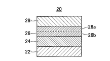
- the piezoelectric thin film element 20 having the potassium sodium niobate (KNN) thin film 26 is produced.
- an object of the present invention is to provide a ferroelectric thin film having excellent electrical characteristics, in particular, leakage current characteristics and ferroelectric characteristics, and a method for producing the same.
- the present invention is a method for producing a ferroelectric thin film, wherein a potassium sodium niobate thin film represented by the general formula (K, Na) NbO 3 is formed using a chemical solution deposition method, A chemical solution deposition solution is applied on a substrate, and a first heat treatment and a second heat treatment are performed to form a potassium sodium niobate layer. The above steps are repeated a predetermined number of times to laminate a potassium sodium niobate layer. Forming a potassium sodium niobate thin film, the thickness of the potassium sodium niobate layer formed in one step is 100 nm or less, and the heating rate of the first heat treatment is 100 ° C./min or more.
- a method for producing a ferroelectric thin film characterized in that the temperature increase rate of the second heat treatment is 15 ° C./min or less.
- the present invention has a leakage current of 2.5 ⁇ 10 5 when a voltage of 100 kV / cm of electric field strength is applied, the main component of which is potassium sodium niobate represented by the general formula (K, Na) NbO 3. -7
- K, Na potassium sodium niobate represented by the general formula (K, Na) NbO 3.
- potassium sodium niobate has a perovskite structure, and although the molar ratio of (K, Na) to Nb is basically 1: 1, it is 1: It may be off from 1 (stoichiometric ratio).
- the first heat treatment (drying treatment) is rapidly performed at a temperature increase rate of 100 ° C./min or more.
- the second heat treatment (firing treatment) is performed slowly at a rate of temperature increase of 15 ° C./min or less.
- the complex formed by reflux is in a stable state up to a relatively high temperature, and decomposes rapidly at around 500 ° C.
- the temperature increase rate of the second heat treatment is high, the volume reduction rate becomes high, and the surface smoothness of the potassium sodium niobate thin film is remarkably deteriorated. Therefore, by setting the rate of temperature rise at the temperature at which the complex is decomposed to 15 ° C./min or less, the rate of volume reduction by heating is reduced, and the surface smoothness of the potassium sodium niobate thin film is improved.
- potassium sodium niobate has poor sinterability. Therefore, if the film thickness before firing is large, K and Na are not uniformly distributed in the potassium sodium niobate thin film when fired. More specifically, an Na excess layer is formed on the upper part of the potassium sodium niobate thin film, and a K excess layer is easily formed on the lower part. Therefore, by setting the thickness of the potassium sodium niobate layer obtained after the end of one firing to 100 nm or less, nonuniform distribution of K and Na is suppressed, and the leakage current characteristics of the potassium sodium niobate thin film Ferroelectric properties are improved.
- the surface smoothness of the potassium sodium niobate thin film is improved and the non-uniform distribution of K and Na in the potassium sodium niobate thin film is suppressed, so that excellent leakage current characteristics and ferroelectric characteristics are obtained.
- a potassium sodium niobate thin film having the following is obtained:
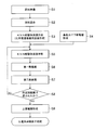
- FIG. 1 is a flowchart showing an embodiment of a method for manufacturing a ferroelectric thin film according to the present invention.
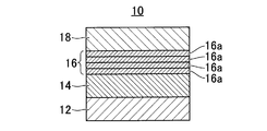
- FIG. 2 is a schematic cross-sectional view of a piezoelectric thin film element 10 having a ferroelectric thin film obtained by the manufacturing method of FIG.
- the piezoelectric thin film element 10 includes a substrate 12, a lower electrode 14 formed on the substrate 12, a ferroelectric thin film 16 formed on the lower electrode 14, and an upper electrode 18 formed on the ferroelectric thin film 16. It is composed of.
- a silicon substrate (Si substrate) is used as the substrate 12.
- the substrate 12 may be a substrate such as a glass substrate, a quartz glass substrate, a GaAs substrate, a GaN substrate, a CaF 2 substrate, a sapphire substrate, an MgO substrate, a SrTiO 3 substrate, a LaAlO 3 substrate, or a stainless steel substrate.
- the ferroelectric thin film 16, that is, the potassium sodium niobate (KNN) thin film 16, is formed by using a chemical solution deposition method.
- Step S1 in FIG. 1 is a step of preparing a raw material for forming a potassium sodium niobate layer, which is the ferroelectric thin film 16.
- the raw materials potassium ethoxide, sodium ethoxide, pentaethoxyniobium, and manganese acetylacetonate are 0.57: 0.67: 0.95 in molar ratio. : Prepared to be 0.02.
- step S2 in FIG. 1 is a step of mixing the raw materials. That is, in step S2, raw materials potassium ethoxide, sodium ethoxide, pentaethoxyniobium, and manganese acetylacetonate are mixed in a 2-methoxyethanol solvent in a glove box.
- step S3 in FIG. 1 a potassium sodium niobate precursor solution is prepared. That is, in step S3, the mixed solution is refluxed at 125 ° C. for 16 hours in a nitrogen atmosphere, whereby a 0.3 M concentration potassium sodium niobate (KNN) precursor solution (also known as a chemical solution deposition solution) is obtained. Called).
- KNN potassium sodium niobate
- step S4 in FIG. 1 is a step of forming the lower electrode 14 on the substrate. That is, in step S4, the lower electrode 14 is formed on the Si substrate 12 by magnetron DC sputtering. As a material of the lower electrode 14, Pt or the like is used.
- the sputtering conditions are a sputtering output of 100 W, a sputtering time of 5 minutes, a temperature of the substrate 12 of 300 ° C., and a degree of vacuum of 5 millitorr. At this time, the thickness of the lower electrode 14 was 250 nm.
- step S5 in FIG. 1 is a step of applying the chemical solution deposition solution created in step 3 to the lower electrode. That is, in step S5, the potassium sodium niobate precursor solution is spin-coated on the lower electrode 14 in a dry gas.
- the thickness of the film to which the chemical solution deposition solution is applied is such that the thickness of the fired potassium sodium niobate layer 16a is 100 nm or less.
- the film thickness of the chemical solution deposition solution applied to form the potassium sodium niobate layer 16a is preferably 5 nm to 120 nm.
- a first heat treatment (preliminary heat treatment or drying treatment) is performed.
- the first heat treatment step which is Step S6, is performed at a temperature increase temperature of 100 ° C./min or more. That is, the potassium sodium niobate precursor solution applied on the lower electrode 14 was heated at a rate of temperature increase of 100 ° C./min or higher using a hot plate previously heated to a temperature of 350 ° C. For 3 minutes.
- the temperature increase rate of the process of 1st heat processing 100 to 3000 degreeC / min is preferable.
- step S7 in FIG. 1 is a step of performing the second heat treatment (main heat treatment or firing treatment) to form the potassium sodium niobate layer 16a.
- the step of the second heat treatment which is Step S7, is performed at a temperature increase rate of 15 ° C./min or less. That is, the dried potassium sodium niobate precursor film has a temperature increase of 15 ° C./min or less in the temperature range of 350 ° C. to 700 ° C. (including the temperature around 500 ° C. at which the complex formed by reflux is rapidly decomposed).
- the temperature is increased at a temperature rate, and firing is performed at a temperature of 700 ° C. for 10 minutes.
- the temperature increase rate in the second heat treatment step is preferably 0.1 ° C./min or more and 15 ° C./min or less.
- the potassium sodium niobate layer 16a is formed.
- the thickness of the potassium sodium niobate layer 16a formed in one step is 100 nm or less.
- 4 nm or more and 100 nm or less are preferable.
- step S8 in FIG. 1 is a step of determining whether or not the formation of the potassium sodium niobate layer 16a in steps S5 to S7 has been repeated a predetermined number of times. That is, in step S8, it is determined whether or not the process of forming the potassium sodium niobate layer 16a has been repeated a predetermined number of times. If the predetermined number of times has not been reached, the process returns to step S5 and again the potassium sodium niobate layer 16a. The process of forming 16a is performed. On the contrary, if the predetermined number of times has been reached, it is determined that the potassium sodium niobate thin film 16 having a predetermined thickness has been formed, and the process proceeds to the next step S9.
- step S9 in FIG. 1 is a step of forming the upper electrode 18 on the potassium sodium niobate thin film 16 formed by the above steps.
- the upper electrode 18 is formed on the potassium sodium niobate thin film 16 by magnetron DC sputtering.
- a material of the upper electrode 18 Pt or the like is used.
- the sputtering conditions are a sputtering output of 100 W, a sputtering time of 5 minutes, a temperature of the substrate 12 of 150 ° C., and a degree of vacuum of 5 millitorr. At this time, the film thickness of the upper electrode 18 was formed at 250 nm. Thus, the piezoelectric thin film element 10 is obtained.
- the first heat treatment (drying treatment) is rapidly performed at a temperature increase rate of 100 ° C./min or more.
- hydrolysis of the raw material in the chemical solution deposition solution that has not reacted when refluxed is suppressed, and the prepared potassium sodium niobate thin film 16 has improved surface smoothness and leakage current. Characteristics and ferroelectric characteristics are improved.
- the second heat treatment (firing treatment) is performed slowly at a rate of temperature increase of 15 ° C./min or less.
- the rate of temperature rise at the temperature at which the complex decomposes (around 500 ° C.) to 15 ° C./min or less, the rate of volume reduction due to heating is reduced, and the surface smoothness of the potassium sodium niobate thin film 16 is reduced. improves.
- the thickness of the potassium sodium niobate layer 16a obtained after the completion of one firing is set to 100 nm or less, the uneven distribution of K and Na is suppressed, and the leakage current of the potassium sodium niobate thin film 16 is reduced. Characteristics and ferroelectric characteristics are improved.
- Table 1 shows that after the first heat treatment, the potassium sodium niobate precursor solution was rapidly heated to 350 ° C. and dried at 350 ° C. for 3 minutes using a hot plate at a heating rate of 100 ° C./min or more.
- the surface roughness of the potassium sodium niobate thin film 16 and the leak current value in an electric field of 100 kV / cm when the temperature increase rate of the second heat treatment is variously changed are shown.
- the rate of temperature increase in the second heat treatment is 100 ° C./min (sample number 1), 50 ° C./min (sample number 2), 30 ° C./min (sample number 3), 15 ° C./min (sample number 4), 10 C./min (sample number 5) and 5 ° C./min (sample number 6).
- the surface roughness (arithmetic mean roughness Ra) of the potassium sodium niobate thin film 16 was measured using a scanning probe microscope “NanoScope” (trade name, manufactured by Digital Instruments).
- the leakage current value in an electric field of 100 kV / cm was measured using a measuring apparatus “Electrometer 6517 type” (trade name, manufactured by Keithley). When the arithmetic average roughness Ra was 4 nm or less and the leakage current was 1 ⁇ 10 ⁇ 5 A / cm 2 or less, it was determined as a good product (G), and otherwise it was determined as a defective product (NG
- the surface of the potassium sodium niobate thin film 16 becomes white and the surface roughness is too large.
- the arithmetic average roughness Ra could not be measured.
- the leak current value also increased as it exceeded the allowable measurement current value of the measuring apparatus, and could not be measured.
- the potassium sodium niobate thin film 16 of sample number 3 has an arithmetic average roughness Ra of 8.6 nm and a leakage current value of 4.5 ⁇ 10 ⁇ 3 A / cm 2, which is a very large value. It was.
- the heating rate of the second heat treatment is 15 ° C./min or less, such as Sample No. 4, Sample No. 5 and Sample No. 6 in the scope of the present invention
- the arithmetic average The roughness Ra is 3.2 nm, 3.1 nm and 3.0 nm, and the leakage current values are 1.1 ⁇ 10 ⁇ 7 A / cm 2 , 7.7 ⁇ 10 ⁇ 8 A / cm 2 and 5.7 ⁇ . It was 10 ⁇ 8 A / cm 2 , which was a very small value.
- the rate of temperature increase in the second heat treatment is as low as 15 ° C./min or less, the rate of volume change of potassium sodium niobate during firing becomes slow, and the arithmetic average roughness Ra and the leakage current value Is improved.
- the potassium sodium niobate thin film 16 of sample numbers 1 to 6 was examined for the distribution of K and Na in the cross section by the energy dispersive X-ray spectroscopy (EDX) method.
- EDX energy dispersive X-ray spectroscopy
- K and Na were distributed unevenly.
- the potassium sodium niobate thin film 16 of Sample No. 3 also showed an improvement compared to Sample Nos. 1 and 2, but K and Na were distributed unevenly.
- K and Na were uniformly distributed.
- Table 2 shows that after the first heat treatment, the potassium sodium niobate precursor solution was slowly heated to 350 ° C. and dried at 350 ° C. for 3 minutes at a heating rate of 10 ° C./min using a hot plate.
- the surface roughness of the potassium sodium niobate thin film 16 and the leak current value in an electric field of 100 kV / cm when the temperature increase rate of the second heat treatment is variously changed are shown.
- the heating rate of the second heat treatment is 100 ° C./min (sample number 7), 50 ° C./min (sample number 8), 30 ° C./min (sample number 9), 15 ° C./min (sample number 10), 10 C./min (sample number 11) and 5 ° C./min (sample number 12).
- Table 3 shows the surface roughness of the potassium sodium niobate thin film 16 and the electric field of 100 kV / cm when the thickness of the potassium sodium niobate layer 16a obtained by one application, drying and baking is variously changed.
- the thickness of the potassium sodium niobate layer 16a is 300 nm (sample number 13), 150 nm (sample number 14), 100 nm (sample number 15), 50 nm (sample number 6), and 30 nm (sample number 16). Note that the number of coating, drying, and firing was adjusted so that the final film thickness of the potassium sodium niobate thin film 16 was 300 nm.
- the arithmetic average roughness Ra was a good value of 3.0 to 3.3 nm in all samples.
- the leakage current value is 2.9 ⁇ 10 ⁇ 3 A / cm 2 and 8 .9 ⁇ 10 ⁇ 4 / cm 2 and a large value.
- the thickness of the potassium sodium niobate layer 16a obtained after one firing is 100 nm or less as in Sample No. 15, Sample No. 6 and Sample No. 16, the leakage current value is 2.5 ⁇ 10. -7 A / cm 2 , 5.7 ⁇ 10 ⁇ 8 A / cm 2, and 3.4 ⁇ 10 ⁇ 8 / cm 2 , showing better leakage current characteristics than Sample Nos. 13 and 14.
- the reason for obtaining a good leak current is that the non-uniform distribution of K and Na is improved by reducing the thickness of the potassium sodium niobate layer 16a obtained after one firing to 100 nm or less. This is because the.
- the rate of temperature increase in the first heat treatment and the second heat treatment and the thickness of the potassium sodium niobate layer 16a obtained after one firing are set within the scope of the present invention, so that the surface smoothness is achieved. It is possible to produce a potassium sodium niobate thin film having excellent properties and insulation properties.
- FIG. 3 shows that the hysteresis curve of the potassium sodium niobate thin film 16 of sample number 3 (defective product) and sample number 5 (good product) is a ferroelectric measuring device “Precision Premeal II” (trade name, manufactured by Radian Technology). ) Shows the result of measurement.
- the present invention improves the surface smoothness and insulation of the potassium sodium niobate thin film 16 to provide a ferroelectric thin film element or piezoelectric thin film element having excellent ferroelectric characteristics. realizable.
Landscapes
- Engineering & Computer Science (AREA)
- Chemical & Material Sciences (AREA)
- Ceramic Engineering (AREA)
- Manufacturing & Machinery (AREA)
- Materials Engineering (AREA)
- Structural Engineering (AREA)
- Organic Chemistry (AREA)
- Dispersion Chemistry (AREA)
- Semiconductor Memories (AREA)
- Formation Of Insulating Films (AREA)
Abstract
L'invention concerne un film mince ferroélectrique ayant d'excellentes caractéristiques électriques, et un procédé de fabrication du film mince ferroélectrique. Un premier traitement thermique (traitement de séchage) est mis en œuvre dans l'étape S6. Une solution de précurseur de niobate de sodium et de potassium, qui a été appliquée sur une électrode inférieure, est chauffée à une vitesse d'augmentation de température d'au moins 100°C/minute à l'aide d'une plaque chauffante qui a été préalablement chauffée à une température de 350°C, et séchée pendant trois minutes. Ensuite, un second traitement thermique (traitement de cuisson) est mis en œuvre dans l'étape S7. Le film précurseur de niobate de sodium et de potassium séché est chauffé jusqu'à 350°C à une vitesse d'augmentation de température d'au moins 100°C/minute à l'aide d'une plaque chauffante chauffée. Le film précurseur de niobate de sodium et de potassium est ensuite chauffé à une vitesse d'augmentation de température non supérieure à 15°C/minute dans les limites d'une plage de températures de 350°C à 700°C, et cuit pendant 10 minutes à 700°C. Une couche de niobate de sodium et de potassium est ainsi formée. L'épaisseur de la couche de niobate de sodium et de potassium formée en une seule application de l'étape précédemment mentionnée est au plus de 100 nm.
Applications Claiming Priority (2)
| Application Number | Priority Date | Filing Date | Title |
|---|---|---|---|
| JP2011090379 | 2011-04-14 | ||
| JP2011-090379 | 2011-04-14 |
Publications (1)
| Publication Number | Publication Date |
|---|---|
| WO2012141104A1 true WO2012141104A1 (fr) | 2012-10-18 |
Family
ID=47009277
Family Applications (1)
| Application Number | Title | Priority Date | Filing Date |
|---|---|---|---|
| PCT/JP2012/059560 Ceased WO2012141104A1 (fr) | 2011-04-14 | 2012-04-06 | Film mince ferroélectrique et son procédé de fabrication |
Country Status (1)
| Country | Link |
|---|---|
| WO (1) | WO2012141104A1 (fr) |
Cited By (4)
| Publication number | Priority date | Publication date | Assignee | Title |
|---|---|---|---|---|
| JP2014207429A (ja) * | 2013-03-19 | 2014-10-30 | 日立金属株式会社 | 圧電薄膜素子、圧電センサ及び振動発電機 |
| JP2015138972A (ja) * | 2014-01-23 | 2015-07-30 | Tdk株式会社 | 薄膜圧電素子、薄膜圧電アクチュエータ、及び薄膜圧電センサ、並びにハードディスクドライブ、及びインクジェットプリンタ装置 |
| EP3382766A1 (fr) * | 2017-03-28 | 2018-10-03 | Seiko Epson Corporation | Composant à couche piézoélectrique |
| US10355196B2 (en) | 2016-02-10 | 2019-07-16 | Seiko Epson Corporation | Piezoelectric element, piezoelectric element application device, and method of manufacturing piezoelectric element |
Citations (6)
| Publication number | Priority date | Publication date | Assignee | Title |
|---|---|---|---|---|
| WO2006035723A1 (fr) * | 2004-09-29 | 2006-04-06 | Ngk Insulators, Ltd. | Element de type film piezoelectrique/d'electrostriction et procede de fabrication de celui-ci |
| JP2007123683A (ja) * | 2005-10-31 | 2007-05-17 | National Institute Of Advanced Industrial & Technology | 強誘電体薄膜の製造方法、強誘電体薄膜 |
| JP2007314378A (ja) * | 2006-05-26 | 2007-12-06 | Seiko Epson Corp | 圧電体層の製造方法 |
| JP2009010367A (ja) * | 2007-05-30 | 2009-01-15 | Canon Inc | 圧電素子、圧電素子の製造方法、圧電アクチュエータおよびインクジェット式記録ヘッド |
| JP2010161330A (ja) * | 2008-12-08 | 2010-07-22 | Hitachi Cable Ltd | 圧電薄膜素子 |
| JP2011109037A (ja) * | 2009-11-20 | 2011-06-02 | Hitachi Cable Ltd | 圧電薄膜素子及び圧電薄膜デバイス |
-
2012
- 2012-04-06 WO PCT/JP2012/059560 patent/WO2012141104A1/fr not_active Ceased
Patent Citations (6)
| Publication number | Priority date | Publication date | Assignee | Title |
|---|---|---|---|---|
| WO2006035723A1 (fr) * | 2004-09-29 | 2006-04-06 | Ngk Insulators, Ltd. | Element de type film piezoelectrique/d'electrostriction et procede de fabrication de celui-ci |
| JP2007123683A (ja) * | 2005-10-31 | 2007-05-17 | National Institute Of Advanced Industrial & Technology | 強誘電体薄膜の製造方法、強誘電体薄膜 |
| JP2007314378A (ja) * | 2006-05-26 | 2007-12-06 | Seiko Epson Corp | 圧電体層の製造方法 |
| JP2009010367A (ja) * | 2007-05-30 | 2009-01-15 | Canon Inc | 圧電素子、圧電素子の製造方法、圧電アクチュエータおよびインクジェット式記録ヘッド |
| JP2010161330A (ja) * | 2008-12-08 | 2010-07-22 | Hitachi Cable Ltd | 圧電薄膜素子 |
| JP2011109037A (ja) * | 2009-11-20 | 2011-06-02 | Hitachi Cable Ltd | 圧電薄膜素子及び圧電薄膜デバイス |
Non-Patent Citations (1)
| Title |
|---|
| YUJI NOGUCHI: "Defect Control for Materials Design of K0.5Na0.5NbO3 Single Crystals", JOURNAL OF THE JAPAN SOCIETY OF APPLIED ELECTROMAGNETICS AND MECHANICS, vol. 15, no. 4, 10 December 2007 (2007-12-10), pages 386 - 390 * |
Cited By (6)
| Publication number | Priority date | Publication date | Assignee | Title |
|---|---|---|---|---|
| JP2014207429A (ja) * | 2013-03-19 | 2014-10-30 | 日立金属株式会社 | 圧電薄膜素子、圧電センサ及び振動発電機 |
| JP2015138972A (ja) * | 2014-01-23 | 2015-07-30 | Tdk株式会社 | 薄膜圧電素子、薄膜圧電アクチュエータ、及び薄膜圧電センサ、並びにハードディスクドライブ、及びインクジェットプリンタ装置 |
| US10355196B2 (en) | 2016-02-10 | 2019-07-16 | Seiko Epson Corporation | Piezoelectric element, piezoelectric element application device, and method of manufacturing piezoelectric element |
| US11417828B2 (en) | 2016-02-10 | 2022-08-16 | Seiko Epson Corporation | Piezoelectric element, piezoelectric element application device, and method of manufacturing piezoelectric element |
| EP3382766A1 (fr) * | 2017-03-28 | 2018-10-03 | Seiko Epson Corporation | Composant à couche piézoélectrique |
| US10937942B2 (en) | 2017-03-28 | 2021-03-02 | Seiko Epson Corporation | Piezoelectric element and piezoelectric element-applied device |
Similar Documents
| Publication | Publication Date | Title |
|---|---|---|
| JP5418725B2 (ja) | 圧電体薄膜素子 | |
| Kang et al. | (1− x) Ba (Zr 0.2 Ti 0.8) O 3–x (Ba 0.7 Ca 0.3) TiO 3 Ferroelectric Thin Films Prepared from Chemical Solutions | |
| CN104040647B (zh) | 热敏电阻用金属氮化物材料及其制造方法以及薄膜型热敏电阻传感器 | |
| Yan et al. | Lead-free (K, Na) NbO3 ferroelectric thin films: Preparation, structure and electrical properties | |
| WO2015060004A1 (fr) | Film mince de diélectrique sans plomb, composition et procédé pour former ce dernier | |
| WO2012141104A1 (fr) | Film mince ferroélectrique et son procédé de fabrication | |
| WO2015060003A1 (fr) | Composition liquide de formation de film mince diélectrique exempt de plomb, procédé de formation dudit film mince et film mince diélectrique exempt de plomb formé au moyen dudit procédé | |
| WO2020045446A1 (fr) | Condensateur à film mince et carte de circuit imprimé électronique | |
| Chen et al. | Low temperature growth of (100)-oriented Ba (Zr0. 2Ti0. 8) O3-0.5 (Ba0. 7Ca0. 3) TiO3 thin films using a LaNiO3 seed layer | |
| Wang et al. | Enhanced dielectric and piezoelectric properties of RF sputtered Pb (Zr0. 60, Ti0. 40) O3 thin films deposited on sol-gel derived Pb1+ x (Zr0. 40, Ti0. 60) O3 seed layer with various lead contents | |
| Xiao et al. | Study of (111)-oriented PZT thin films prepared by a modified sol–gel method | |
| Vitanov et al. | Deposition, structure evolution and dielectric properties of BaTiO3 and BaxSr1− xTiO3 thin films prepared by the sol–gel method | |
| WO2014185274A1 (fr) | Substrat de silicium avec film ferroélectrique | |
| Dong et al. | Effects of substrate on the crystalline structure and microwave dielectric properties of Bi1. 5Mg1. 0Nb1. 5O7 sol–gel thin films | |
| Zheng et al. | The effects of annealing temperature on the properties of Bi3. 15Nd0. 85Ti3O12 thin films | |
| Suzuki et al. | Sol–gel synthesis of high‐k HfO2 thin films | |
| CN104072131B (zh) | 铁电薄膜形成用组合物的制造方法及其用途 | |
| JP5136986B2 (ja) | 圧電体の製造方法および圧電素子 | |
| Kumar et al. | Effect of substrates on phase formation in PMN-PT 68/32 thin films by sol–gel process | |
| JP3438509B2 (ja) | セラミックス薄膜及びその製造方法 | |
| JP2002324924A (ja) | 圧電素子の製造方法 | |
| Takahashi et al. | Thermal stability of SrRuO3 bottom electrode and electric property of Pb (Zr, Ti) O3 thin film deposited on SrRuO3 | |
| JPH09213569A (ja) | 積層誘電体およびコンデンサ | |
| Nurbaya et al. | Structural and electrical properties of sol–gel-derived lead titanate nanofilms with different Pb contents for MIM capacitors | |
| KR101138239B1 (ko) | 고압전 계수 박막의 제조방법 |
Legal Events
| Date | Code | Title | Description |
|---|---|---|---|
| 121 | Ep: the epo has been informed by wipo that ep was designated in this application |
Ref document number: 12770645 Country of ref document: EP Kind code of ref document: A1 |
|
| NENP | Non-entry into the national phase |
Ref country code: DE |
|
| 122 | Ep: pct application non-entry in european phase |
Ref document number: 12770645 Country of ref document: EP Kind code of ref document: A1 |
|
| NENP | Non-entry into the national phase |
Ref country code: JP |