WO2012143970A1 - Synthétiseur de fréquence - Google Patents
Synthétiseur de fréquence Download PDFInfo
- Publication number
- WO2012143970A1 WO2012143970A1 PCT/JP2011/002283 JP2011002283W WO2012143970A1 WO 2012143970 A1 WO2012143970 A1 WO 2012143970A1 JP 2011002283 W JP2011002283 W JP 2011002283W WO 2012143970 A1 WO2012143970 A1 WO 2012143970A1
- Authority
- WO
- WIPO (PCT)
- Prior art keywords
- signal
- output
- synchronization
- control voltage
- phase difference
- Prior art date
- Legal status (The legal status is an assumption and is not a legal conclusion. Google has not performed a legal analysis and makes no representation as to the accuracy of the status listed.)
- Ceased
Links
Images


Classifications
-
- H—ELECTRICITY
- H03—ELECTRONIC CIRCUITRY
- H03L—AUTOMATIC CONTROL, STARTING, SYNCHRONISATION OR STABILISATION OF GENERATORS OF ELECTRONIC OSCILLATIONS OR PULSES
- H03L7/00—Automatic control of frequency or phase; Synchronisation
- H03L7/06—Automatic control of frequency or phase; Synchronisation using a reference signal applied to a frequency- or phase-locked loop
- H03L7/08—Details of the phase-locked loop
- H03L7/085—Details of the phase-locked loop concerning mainly the frequency- or phase-detection arrangement including the filtering or amplification of its output signal
- H03L7/087—Details of the phase-locked loop concerning mainly the frequency- or phase-detection arrangement including the filtering or amplification of its output signal using at least two phase detectors or a frequency and phase detector in the loop
-
- H—ELECTRICITY
- H03—ELECTRONIC CIRCUITRY
- H03L—AUTOMATIC CONTROL, STARTING, SYNCHRONISATION OR STABILISATION OF GENERATORS OF ELECTRONIC OSCILLATIONS OR PULSES
- H03L7/00—Automatic control of frequency or phase; Synchronisation
- H03L7/06—Automatic control of frequency or phase; Synchronisation using a reference signal applied to a frequency- or phase-locked loop
- H03L7/08—Details of the phase-locked loop
- H03L7/085—Details of the phase-locked loop concerning mainly the frequency- or phase-detection arrangement including the filtering or amplification of its output signal
-
- H—ELECTRICITY
- H03—ELECTRONIC CIRCUITRY
- H03L—AUTOMATIC CONTROL, STARTING, SYNCHRONISATION OR STABILISATION OF GENERATORS OF ELECTRONIC OSCILLATIONS OR PULSES
- H03L7/00—Automatic control of frequency or phase; Synchronisation
- H03L7/06—Automatic control of frequency or phase; Synchronisation using a reference signal applied to a frequency- or phase-locked loop
- H03L7/08—Details of the phase-locked loop
- H03L7/10—Details of the phase-locked loop for assuring initial synchronisation or for broadening the capture range
- H03L7/113—Details of the phase-locked loop for assuring initial synchronisation or for broadening the capture range using frequency discriminator
-
- H—ELECTRICITY
- H03—ELECTRONIC CIRCUITRY
- H03L—AUTOMATIC CONTROL, STARTING, SYNCHRONISATION OR STABILISATION OF GENERATORS OF ELECTRONIC OSCILLATIONS OR PULSES
- H03L7/00—Automatic control of frequency or phase; Synchronisation
- H03L7/06—Automatic control of frequency or phase; Synchronisation using a reference signal applied to a frequency- or phase-locked loop
- H03L7/16—Indirect frequency synthesis, i.e. generating a desired one of a number of predetermined frequencies using a frequency- or phase-locked loop
- H03L7/18—Indirect frequency synthesis, i.e. generating a desired one of a number of predetermined frequencies using a frequency- or phase-locked loop using a frequency divider or counter in the loop
- H03L7/197—Indirect frequency synthesis, i.e. generating a desired one of a number of predetermined frequencies using a frequency- or phase-locked loop using a frequency divider or counter in the loop a time difference being used for locking the loop, the counter counting between numbers which are variable in time or the frequency divider dividing by a factor variable in time, e.g. for obtaining fractional frequency division
Definitions
- the present invention relates to a fractional-N type phase-locked loop type frequency synthesizer used in, for example, a radio communication apparatus.
- FIG. 21 is a block diagram showing a phase-locked loop type frequency synthesizer of the fractional-N system disclosed in the following non-patent document 1. Hereinafter, the operation of the frequency synthesizer of FIG. 21 will be described.
- the reference signal source 101 generates a reference signal REF and outputs the reference signal REF to the phase comparator 104.
- the variable frequency divider 102 (indicated as “ ⁇ N” in FIG. 21) divides the high frequency signal output from the voltage controlled oscillator 107 in accordance with the frequency division data output from the modulation circuit 103, and divides the high frequency signal.
- the high-frequency signal after the round is output to the phase comparator 104 as the synchronization signal DIV.
- the modulation circuit 103 operates in synchronization with either the reference signal generated by the reference signal source 101 or the synchronization signal output from the variable frequency divider 102, and the variable frequency divider according to a setting signal given from the outside.
- the frequency division number of 102 is determined, and frequency division data indicating the frequency division number is output to the variable frequency divider 102.
- the phase comparator 104 (denoted as “DEF-PD” in FIG. 21) is configured using a D-type flip-flop, and the reference signal REF output from the reference signal source 101 and the variable frequency divider
- the phase difference signals D and U corresponding to the phase difference of the synchronization signal DIV output from 102 are output to the charge pump 105.
- the charge pump 105 (indicated as “CP” in FIG. 21) outputs the charge pump current I i corresponding to the phase difference signals D and U output from the phase comparator 102 to the current output corresponding loop filter 106. To do.
- the current output corresponding loop filter 106 (indicated as “I-LF” in FIG. 21) performs voltage control using a smoothed voltage of the charge pump current I i output from the charge pump 105 as a control voltage V t. Output to the oscillator 107.
- the voltage controlled oscillator 107 receives the control voltage V t from the current output corresponding loop filter 106, the voltage controlled oscillator 107 generates a high frequency signal having a frequency corresponding to the control voltage V t and outputs the high frequency signal to the variable frequency divider 102 and the outside. To do.
- FIG. 22 is a block diagram showing the inside of the phase comparator 104 and the charge pump 105 in the frequency synthesizer.
- the D-type flip-flop 111 (denoted as “D-FF” in FIG. 22) of the phase comparator 104 receives the reference signal REF and the reset signal RST output from the reference signal source 101, and receives the reference signal.
- the rising edge detection signal D of REF is output to the AND circuit 113 and the switch 116 of the charge pump 105.
- the D-type flip-flop 112 receives the synchronization signal DIV and the reset signal RST output from the variable frequency divider 102, and the rising edge of the synchronization signal DIV
- the detection signal U is output to the AND circuit 113 and the switch 117 of the charge pump 105.
- the AND circuit 113 (indicated as “AND” in FIG. 22) inputs the rising edge detection signal D output from the D-type flip-flop 111 and the rising edge detection signal U output from the D-type flip-flop 112. Then, the AND operation of the rising edge detection signal D and the rising edge detection signal U is performed, and the calculation result is output to the D flip-flops 111 and 112 as the reset signal RST.
- the constant current source 115 of the charge pump 105 is connected to the power supply circuit 114 and generates a predetermined current I i .
- the constant current source 118 is connected to the ground terminal 119, generates a predetermined current I i, and outputs the current I i toward the ground terminal 119.
- the switch 116 (denoted as “SW” in FIG. 22) is turned on when it receives the rising edge detection signal D from the D-type flip-flop 111 of the phase comparator 104.
- the switch 117 (denoted as “SW” in FIG. 22) is turned on when the rising edge detection signal U is received from the D-type flip-flop 112 of the phase comparator 104.
- FIG. 23 shows waveforms of the respective parts of the phase comparator 104 and the charge pump 105 when the cycle T of the reference signal REF is “4” and the cycle T of the synchronization signal DIV is “6” and “2”. It is explanatory drawing shown. For example, when the rising edge of the synchronization signal DIV is input earlier than the reference signal REF, only the rising edge detection signal U changes from logic low to logic high. When the rising edge of the reference signal REF is detected, the rising edge detection signal D changes from logic low to logic high.
- the D-type flip-flops 111 and 112 are reset, and the rising edge detection signals U and D change to logic low.
- the switch 117 is turned on, and a current I i flows from the outside toward the ground terminal 119. At this time, since the current is sucked into the charge pump 105 from the outside, the current I i flows in a negative direction.
- the rising edge detection signal D changes from logic low to logic high.
- the rising edge detection signal U changes from logic low to logic high.
- the reset signal RST also changes from logic low to logic high, the D-type flip-flops 111 and 112 are reset, and the rising edge detection signals U and D change to logic low.
- the switch 116 is turned on, and a current I i flows from the power supply circuit 114 to the outside. At this time, the current I i flows in a positive direction.
- the time difference between the rising edges of the reference signal REF and the synchronization signal DIV is different between the reference signal REF and the synchronization signal DIV. Is treated as a phase difference.
- the current output corresponding loop filter 106 controls the high frequency signal generated from the voltage controlled oscillator 107 to have a desired frequency.
- a voltage V t is output to the voltage controlled oscillator 107.
- the integration result of the current I i for one cycle of the frequency-dividing pattern that changes with time is ideally zero, and the control voltage V t is maintained at a predetermined voltage. Note that the integration result becomes zero under the condition that the DC gain of the current output loop filter 106 is infinite. Actually, although the DC gain is not infinite, it is a very large value, so that the integration result is almost zero.
- FIG. 24 is a block diagram showing a phase-locked loop type frequency synthesizer disclosed in Non-Patent Document 2 below.
- a phase comparator 108 composed of an EX-OR circuit is used.
- the operation of the frequency synthesizer of FIG. 24 will be described.
- the phase comparator 108 (denoted as “EX-OR” in FIG. 24), which is an EX-OR circuit, is synchronized with the reference signal REF output from the reference signal source 101 and the synchronous frequency output from the variable frequency divider 102.
- the signal DIV is input, and phase difference signals OUT and OUTB corresponding to the phase difference between the reference signal REF and the synchronization signal DIV are output to the voltage output corresponding loop filter 109.
- OUTB is a pair of OUT differential signals.
- the voltage output corresponding loop filter 109 (denoted as “V-LF” in FIG. 24) uses the smoothed voltage of the phase difference signals OUT and OUTB output from the phase comparator 108 as the control voltage V t . Output to the voltage controlled oscillator 107.
- FIG. 25 shows each part of the phase comparator 108 (EX-OR circuit) when the cycle T of the reference signal REF is “4” and the cycle T of the synchronization signal DIV is “6” and “2”. It is explanatory drawing which shows a waveform.
- the phase comparator 108 that is an EX-OR circuit when the reference signal REF that is an input signal and the synchronization signal DIV are in the same state (both signals are logic high or both signals are logic low), the phase difference signal OUT is logic low, and the phase difference signal OUTB is logic high.
- phase difference signal OUT is logic high and the phase difference signal OUTB is logic low.
- the difference signal OUTB-OUT is a voltage signal centered on zero.
- the time difference between the state (logic high or logic low) of the reference signal REF and the synchronization signal DIV is different between the reference signal REF and the synchronization signal DIV. Is treated as a phase difference.
- the difference signal is set so that the high frequency signal generated from the voltage controlled oscillator 107 has a desired frequency.
- the control voltage V t is output from the voltage output corresponding loop filter 109 to the voltage controlled oscillator 107.
- the integration result corresponding to one period of the difference signal of the frequency division number of patterns to be time-varying is ideally zero and the control voltage V t is maintained at a predetermined voltage. Note that the integration result becomes zero under the condition that the DC gain of the voltage output loop filter 109 is infinite. Actually, although the DC gain is not infinite, it is a very large value, so that the integration result is almost zero.
- phase comparator 104 When the phase comparator 104 composed of the D-type flip-flops 111 and 112 is compared with the phase comparator 108 composed of the EX-OR circuit, the phase comparator 104 determines the D-type flip-flop according to the phase difference of the input signal.
- the detection signals output from the loops 111 and 112 change.
- the EX-OR circuit since the EX-OR circuit is composed of a single circuit, the operation location for the phase difference of the input signal does not change.
- FIG. 26 is an explanatory diagram showing detection characteristics with respect to a phase difference in the case where the phase comparator 104 includes D-type flip-flops 111 and 112.
- the detection characteristic with respect to the phase difference is a straight line (detection characteristic indicated by a dotted line).
- error factors such as variations in the current values of the constant current sources 115 and 118 and delays in operation timing between the circuits in the D-type flip-flops 111 and 112
- a difference occurs in the slope of the detection characteristics.
- a non-linear change occurs near zero in the phase difference.
- the phase comparator 104 is composed of D-type flip-flops 111 and 112
- the detection signal is output because the phase difference between the reference signal REF and the synchronization signal DIV is mainly negative or positive depending on the frequency division number.
- the D-type flip-flops 111 and 112 to be changed are affected by the nonlinearity of the detection characteristic as shown in FIG. As a result, spurious is generated in the high-frequency signal that is the output of the frequency synthesizer. Further, when this spurious is near the carrier wave, the out-of-band suppression effect due to the closed-loop transfer characteristic of the PLL cannot be obtained.
- FIG. 27 is an explanatory diagram showing waveforms of respective parts of the EX-OR circuit when the reference signal REF and the synchronization signal DIV having the same rising edge as in FIG. 25 are input. The difference between FIG. 25 and FIG. 27 is the duty ratio of the waveform of the synchronization signal DIV whose period T is “6”.
- the integration result of the difference signal (OUTB-OUT) for one period of the time change pattern is greater than zero. Specifically, among the period T of “8”, the period T of “6” is logic high and the period T of “2” is logic low. As described above, when the phase comparator 108 including the EX-OR circuit is used, the comparison result of the phase comparator 108 varies when the duty ratio of the input signal changes. As a result, spurious is generated in the high-frequency signal that is the output of the frequency synthesizer.
- FIG. 28 shows waveforms of respective parts of the phase comparator 108 (EX-OR circuit) when the cycle T of the reference signal REF is “8” and the cycle T of the synchronization signal DIV is “6” and “2”. It is explanatory drawing.
- the average of the period T of the synchronization signal DIV is “4”, which is different from the period T “8” of the reference signal REF.
- the integration result of the difference signal (OUTB-OUT) for one period of the time change pattern becomes zero, and phase synchronization is established. That is, the phase comparator 108 composed of an EX-OR circuit cannot perform wideband frequency control.
- the phase comparator 104 is configured by D-type flip-flops 111 and 112
- the phase comparator 108 is configured by an EX-OR circuit.
- problems such as spurious generation in the high-frequency signal that is output.
- the present invention has been made to solve the above-described problems, and an object thereof is to obtain a frequency synthesizer capable of realizing low spurious characteristics.
- a frequency synthesizer is generated by a reference signal source that generates a reference signal, a synchronization signal output circuit that divides a high-frequency signal and outputs the divided high-frequency signal as a synchronization signal, and a reference signal source
- a phase difference detection circuit that detects a phase difference between the reference signal and the synchronization signal output from the synchronization signal output circuit, and outputs a control voltage corresponding to the phase difference, and a control voltage output from the phase difference detection circuit.
- a first phase comparator that generates a signal
- a first control voltage generation circuit that generates a control voltage according to the phase difference signal generated by the first phase comparator, and a synchronization signal
- a first flip-flop that inverts the amplitude of the output signal
- an inverter that inverts the amplitude of the reference signal
- a signal edge of the reference signal after the amplitude inversion by the inverter is detected
- the second flip-flop for inverting the amplitude of the output signal and the second phase comparison for calculating the exclusive OR of the output signals of the first and second flip-flops and outputting the phase difference signal indicating the calculation result
- a second control voltage generation circuit for generating a control voltage corresponding to the phase difference signal output from the second phase comparator, and a phase synchronization signal from the phase difference signal generated by the first phase comparator.
- the control voltage generated by the first control voltage generation circuit is output to the voltage controlled oscillator, and the synchronization detection circuit If it is detected phase synchronization established by, those which are constituted by a control voltage selecting means for outputting a control voltage generated by the second control voltage generating circuit to the voltage controlled oscillator.
- the phase difference detection circuit generates the phase difference signal from the detection timing of the signal edge in the reference signal and the synchronization signal, and the phase difference generated by the first phase comparator.
- a first control voltage generating circuit for generating a control voltage according to the signal, a first flip-flop for inverting the amplitude of the output signal each time a signal edge of the synchronization signal is detected, and an amplitude of the reference signal
- a second control for generating a control voltage corresponding to the phase difference signal output from the second phase comparator.
- a pressure detection circuit for detecting establishment of phase synchronization from the phase difference signal generated by the first phase comparator, and a first control voltage if the establishment of phase synchronization is not detected by the synchronization detection circuit
- the control voltage generated by the generation circuit is output to the voltage controlled oscillator, and if the establishment of phase synchronization is detected by the synchronization detection circuit, the control voltage generated by the second control voltage generation circuit is output to the voltage controlled oscillator. Since the control voltage selecting means is used, low spurious characteristics can be realized.
- FIG. 6 is an explanatory diagram showing waveforms at various parts of the -OR circuit 19; It is a block diagram which shows the other frequency synthesizer by Embodiment 1 of this invention.
- FIG. 3 is a configuration diagram showing a voltage output corresponding loop filter 20.
- FIG. 3 is a configuration diagram showing a voltage output corresponding loop filter 20.
- FIG. 1 is a block diagram showing a fractional-N phase-locked loop type frequency synthesizer disclosed in Non-Patent Document 1.
- FIG. 2 is a configuration diagram showing the inside of a phase comparator 104 and a charge pump 105 in a frequency synthesizer.
- FIG. FIG. 10 is an explanatory diagram showing waveforms of respective parts of the phase comparator 104 and the charge pump 105 when the cycle T of the reference signal REF is “4” and the cycle T of the synchronization signal DIV is “6” and “2”.
- FIG. 7 is an explanatory diagram showing waveforms of respective parts of the phase comparator (EX-OR circuit) when the cycle T of the reference signal REF is “4” and the cycle T of the synchronization signal DIV is “6” and “2”. is there.
- FIG. 26 is an explanatory diagram showing waveforms of respective parts of the EX-OR circuit when a reference signal REF and a synchronization signal DIV having the same rising edge as FIG.
- FIG. 7 is an explanatory diagram showing waveforms of respective parts of the phase comparator (EX-OR circuit) when the cycle T of the reference signal REF is “8” and the cycle T of the synchronization signal DIV is “6” and “2”. is there.
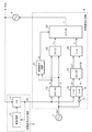
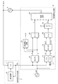
- FIG. 1 is a block diagram showing a frequency synthesizer according to Embodiment 1 of the present invention.
- a reference signal source 1 is a signal source that generates a reference signal REF and outputs the reference signal REF to the phase difference detection circuit 3.
- the synchronization signal output circuit 2 divides the high frequency signal output from the voltage controlled oscillator 4 and outputs the divided high frequency signal to the phase difference detection circuit 3 as the synchronization signal DIV.
- the phase difference detection circuit 3 detects a phase difference between the reference signal REF generated by the reference signal source 1 and the synchronization signal DIV output from the synchronization signal output circuit 2, and a control voltage V t (V t1) corresponding to the phase difference. Or a circuit that outputs V t2 ) to the voltage controlled oscillator 4.
- the voltage controlled oscillator 4 generates a high frequency signal having a frequency corresponding to the control voltage V t (V t1 or V t2 ) output from the phase difference detection circuit 3, and outputs the high frequency signal to the synchronization signal output circuit 2 and the outside. It is an oscillator.
- a variable frequency divider 11 (indicated as “ ⁇ N” in FIG. 1) of the synchronization signal output circuit 2 outputs a high frequency signal output from the voltage controlled oscillator 4 according to the frequency-divided data output from the modulation circuit 12.
- a process of dividing the frequency and outputting the divided high-frequency signal to the phase difference detection circuit 3 as the synchronization signal DIV is performed.
- the modulation circuit 12 operates in synchronization with either the reference signal REF generated by the reference signal source 1 or the synchronization signal DIV output from the variable frequency divider 11, and variable frequency division according to a setting signal given from the outside.
- the frequency division number of the frequency divider 11 is determined, and the frequency division data indicating the frequency division number is output to the variable frequency divider 11.
- the D-type flip-flop 13 (denoted as “DEF-PD” in FIG. 1), which is the first phase comparator of the phase difference detection circuit 3, outputs the reference signal REF output from the reference signal source 1 and the variable component. Processing for generating the phase difference signals D and U from the detection timing of the signal edge in the synchronization signal DIV output from the frequency divider 11 is performed. That is, the D-type flip-flop 13 outputs to the charge pump 14 phase difference signals D and U corresponding to the phase difference between the reference signal REF output from the reference signal source 1 and the synchronization signal DIV output from the variable frequency divider 11. Perform the process.
- the charge pump 14 (indicated as “CP” in FIG. 1) outputs the charge pump current I i corresponding to the phase difference signals D and U output from the D-type flip-flop 13 to the current output corresponding loop filter 15. Perform the process.
- the current output loop filter 15 (denoted as “I-LF” in FIG. 1) applies a voltage obtained by smoothing the charge pump current I i output from the charge pump 14 to the switch 22 as a control voltage V t1. Perform the output process.
- the charge pump 14 and the current output loop filter 15 constitute a first control voltage generation circuit.
- T-FF T-type flip-flop 16
- T-FF T-FF
- the inverter 17 is an element that inverts the amplitude of the reference signal REF output from the reference signal source 1.
- the T-type flip-flop 18 (denoted as “T-FF” in FIG. 1), which is the second flip-flop, outputs the output signal every time the signal edge of the reference signal REF after the amplitude inversion by the inverter 17 is detected. The process of inverting the amplitude of is performed.
- the EX-OR circuit 19 (denoted as “EX-OR” in FIG. 1), which is the second phase comparator, excludes the output signal of the T-type flip-flop 16 and the output signal of the T-type flip-flop 18.
- a process of calculating a logical OR and outputting the phase difference signals OUT and OUTB indicating the calculation result to the voltage output corresponding loop filter 20 is performed. Note that OUT and OUTB form a pair of differential signals.
- a voltage output corresponding loop filter 20 (indicated as “V-LF” in FIG. 1) as a second control voltage generation circuit smoothes the phase difference signals OUT and OUTB output from the EX-OR circuit 19.
- a process of outputting the obtained voltage to the switch 22 as the control voltage V t2 is performed.
- the synchronization detection circuit 21 performs processing for detecting establishment of phase synchronization from the phase difference signals D and U generated by the D-type flip-flop 13. If the establishment of phase synchronization is not detected by the synchronization detection circuit 21, the switch 22 that is a control voltage selection unit selects the control voltage V t1 generated by the current output corresponding loop filter 15 and uses the control voltage V t1 as a voltage. and outputs the controlled oscillator 4, if it is detected in the phase synchronization established by the synchronization detection circuit 21 selects the control voltage V t2 which is generated by the voltage output corresponding loop filter 20, a voltage controlled oscillator the control voltage V t2 The process which outputs to 4 is implemented.
- the reference signal source 1 generates a reference signal REF and outputs the reference signal REF to the D-type flip-flop 13 and the inverter 17 of the phase difference detection circuit 3.
- the duty ratio of the reference signal REF is 50%.
- the variable frequency divider 11 of the synchronization signal output circuit 2 divides a high-frequency signal output from a voltage controlled oscillator 4 described later according to the frequency-divided data output from the modulation circuit 12, and the divided high-frequency signal is output.
- the synchronization signal DIV is output to the D-type flip-flop 13 and the T-type flip-flop 16 of the phase difference detection circuit 3.
- the modulation circuit 12 of the synchronization signal output circuit 2 operates in synchronization with either the reference signal REF generated by the reference signal source 1 or the synchronization signal DIV output from the variable frequency divider 11, and is supplied from the outside.
- the frequency division number of the variable frequency divider 11 is determined according to the set signal to be output, and the frequency division data indicating the frequency division number is output to the variable frequency divider 11.
- the D-type flip-flop 13 of the phase difference detection circuit 3 receives the reference signal REF from the reference signal source 1 and receives the synchronization signal DIV from the variable frequency divider 11, the D-type flip-flop 13 responds to the phase difference between the reference signal REF and the synchronization signal DIV.
- the phase difference signals D and U are output to the charge pump 14.
- the charge pump 14 receives the phase difference signals D and U from the D-type flip-flop 13, it outputs a charge pump current I i corresponding to the phase difference signals D and U to the current output corresponding loop filter 15.
- the D-type flip-flop 13 and the charge pump 14 are configured as shown in FIG. 22 (in FIG. 22, the phase comparator 104 corresponds to the D-type flip-flop 13 and the charge pump 105 corresponds to the charge pump 14.
- D-type flip-flop 13 and charge pump 14 operate as follows.
- the D-type flip-flop 111 receives the reference signal REF and the reset signal RST output from the reference signal source 1, and outputs the rising edge detection signal D of the reference signal REF to the AND circuit 113 and the switch 116 of the charge pump 14. .
- the D-type flip-flop 112 receives the synchronization signal DIV and the reset signal RST output from the variable frequency divider 11, and outputs the rising edge detection signal U of the synchronization signal DIV to the AND circuit 113 and the switch 117 of the charge pump 14. To do.
- the AND circuit 113 receives the rising edge detection signal D output from the D-type flip-flop 111 and the rising edge detection signal U output from the D-type flip-flop 112, and the rising edge detection signal D and the rising edge detection signal U. And the operation result is output to the D flip-flops 111 and 112 as the reset signal RST.
- the constant current source 115 is connected to the power supply circuit 114 and generates a predetermined current I i .
- the constant current source 118 is connected to the ground terminal 119, generates a predetermined current I i, and outputs the current I i toward the ground terminal 119.
- the switch 116 is turned on upon receiving the rising edge detection signal D from the D-type flip-flop 111.
- the switch 117 is turned on when the rising edge detection signal U is received from the D-type flip-flop 112.
- the current output corresponding loop filter 15 When receiving the charge pump current I i from the charge pump 14, the current output corresponding loop filter 15 outputs a voltage obtained by smoothing the charge pump current I i to the switch 22 as the control voltage V t1 .
- the T-type flip-flop 16 When the T-type flip-flop 16 receives the synchronization signal DIV from the variable frequency divider 11, the T-type flip-flop 16 performs signal edge detection processing of the synchronization signal DIV, and each time the signal edge of the synchronization signal DIV is detected, The amplitude is inverted (the state of the output signal is inverted from logic high to logic low, or from logic low to logic high), and the signal D 1 after amplitude inversion is output to the EX-OR circuit 19.
- the inverter 17 When receiving the reference signal REF from the reference signal source 1, the inverter 17 inverts the amplitude of the reference signal REF and outputs the reference signal REF after the amplitude inversion to the T-type flip-flop 18.
- the T-type flip-flop 18 performs processing for detecting the signal edge of the reference signal REF after the amplitude inversion by the inverter 17, and inverts the amplitude of the output signal every time the signal edge of the reference signal REF is detected (the output signal The state is inverted from logic high to logic low, or from logic low to logic high), and the signal R1 after amplitude inversion is output to the EX-OR circuit 19.
- the EX-OR circuit 19 calculates an exclusive OR of the output signal D1 of the T-type flip-flop 16 and the output signal R1 of the T-type flip-flop 18, and outputs voltage signals of phase difference signals OUT and OUTB indicating the calculation result. Output to the corresponding loop filter 20. OUT and OUTB form a differential signal pair.
- the voltage output corresponding loop filter 20 outputs a voltage obtained by smoothing the phase difference signals OUT and OUTB to the switch 22 as a control voltage Vt2 .
- the synchronization detection circuit 21 detects the establishment of phase synchronization from the phase difference signals D and U.
- the synchronization detection circuit 21 is a logic low indicating that phase synchronization is not established.
- the synchronization signal LD is output to the switch 22.
- the synchronization detection circuit 21 indicates a logic high indicating that phase synchronization is established. Is output to the switch 22.
- the switch 22 When the switch 22 receives a logic low synchronization signal LD indicating that phase synchronization is not established from the synchronization detection circuit 21, the switch 22 selects the control voltage V t1 generated by the current output corresponding loop filter 15 and controls the control voltage V t1. The voltage V t1 is output to the voltage controlled oscillator 4.
- the switch 22 receives the logic high synchronization signal LD indicating that phase synchronization is established from the synchronization detection circuit 21, the switch 22 selects the control voltage V t2 generated by the voltage output corresponding loop filter 20 and controls the control voltage V t2.
- the voltage V t2 is output to the voltage controlled oscillator 4.
- Voltage controlled oscillator 4 receives a control voltage V t (V t1 or V t2) from the phase difference detecting circuit 3 generates a frequency of the high-frequency signal corresponding to the control voltage V t (V t1 or V t2), The high-frequency signal is output to the synchronization signal output circuit 2 and the outside.
- the control voltage V t1 or the EX-OR circuit generated from the phase difference signals D and U that are the outputs of the D-type flip-flop 13 depending on the phase synchronization state.
- the control voltage V t2 generated from the phase difference signals OUT and OUTB which are the outputs of 19 is selected, and a high frequency signal is generated.
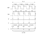
- FIG. 2 shows a D-type flip-flop when the cycle T of the reference signal REF is “4.25” and the cycle T of the synchronization signal DIV is “4”, “4”, “4”, “5”.
- FIG. 7 is an explanatory diagram showing waveforms of respective parts of the pump 13 and the charge pump 14.
- the duty ratio of the reference signal REF is 50%
- the duty ratio of the synchronization signal DIV whose cycle T is “4” is 25%
- the duty ratio of the synchronization signal DIV whose cycle T is “5” is 20%.
- the D-type flip-flop 13 Since the D-type flip-flop 13 detects the time difference between the rising edges of the reference signal REF and the synchronization signal DIV as a phase difference, it is not affected by the duty ratio of the synchronization signal DIV that varies according to the period T.
- the integration result of the charge pump current I i for one cycle of the frequency-dividing frequency pattern ideally becomes zero, and the control voltage V t1 is maintained at a predetermined voltage.
- the operation described above is the same as the operation of the phase comparator of the conventional frequency synthesizer disclosed in Non-Patent Document 1 and Non-Patent Document 2.
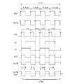
- FIG. 3 shows a T-type flip-flop 16 when the cycle T of the reference signal REF is “4.25” and the cycle T of the synchronization signal DIV is “4”, “4”, “4”, “5”.
- 18 is an explanatory diagram showing waveforms at various parts of the EX-OR circuit 19 and FIG.
- the duty ratio of the reference signal REF is 50%
- the duty ratio of the synchronization signal DIV whose cycle T is “4” is 25%
- the duty ratio of the synchronization signal DIV whose cycle T is “5” is 20%.
- signals (R1, D1) in which the state becomes logic high or logic low for a period of one cycle of the reference signal REF and the synchronization signal DIV are generated.
- the EX-OR circuit 19 detects the time difference between the states of the signals R1 and D1 representing the period time as a phase difference, thereby eliminating the influence of the duty ratio of the synchronization signal DIV that varies according to the period.
- the integration result of the difference signal (OUTB-OUT) for one period of the time change pattern is ideally zero, and the control voltage Vt2 is maintained at a predetermined voltage.
- the phase difference detection circuit 3 generates the phase difference signals D and U from the detection timing of the signal edge in the reference signal REF and the synchronization signal DIV. 13, the current output corresponding loop filter 15 that generates the control voltage V t1 according to the phase difference signals D and U generated by the D-type flip-flop 13, and the output signal every time the signal edge of the synchronization signal DIV is detected.
- T-type flip-flop 16 that inverts the amplitude of the reference signal
- inverter 17 that inverts the amplitude of the reference signal REF
- T that inverts the amplitude of the output signal each time the signal edge of the reference signal after the amplitude inversion by the inverter 17 is detected.
- EX-OR circuit 19 for outputting signals OUT and OUTB
- loop filter 20 for voltage output for generating control voltage V t2 corresponding to phase difference signals OUT and OUTB output from EX-OR circuit 19, and D-type flip-flop
- the phase detection signal 21 is not detected by the synchronization detection circuit 21 and the synchronization detection circuit 21 detects the establishment of the phase synchronization from the phase difference signals D and U generated by the loop 13, the current output corresponding loop filter 15
- the control voltage V t1 is output to the voltage controlled oscillator 4, and if the establishment of phase synchronization is detected by the synchronization detection circuit 21, the control voltage V t2 generated by the voltage output corresponding loop filter 20 is output to the voltage controlled oscillator 4. Therefore, an effect of realizing low spurious characteristics can be achieved.
- the first embodiment it is possible to solve the problem of the conventional example in which a D-type flip-flop or an EX-OR circuit is used alone as a phase comparator of a frequency synthesizer.
- First by using the output of the EX-OR circuit 19 instead of using the output of the D-type flip-flop 13 after the phase synchronization is established, the spurious caused by the variation between the circuits in the D-type flip-flop 13 is eliminated. Does not occur.
- Second by making the input of the EX-OR circuit 19 the signals (R1, D1) representing the period of the reference signal REF and the synchronization signal DIV, spurious due to the change in the duty ratio of the synchronization signal DIV does not occur.
- the control voltage V t is changed from V t1 to V t2 by the switch 22 after the establishment of phase synchronization. discontinuity of the control voltage V t when switching is not present in the ideal. That is, there is no change in the output frequency due to switching of the switch 22.
- the duty ratio of the reference signal REF is 50%.
- the control voltage V t is controlled by the switch 22 after the phase synchronization is established. Is switched from V t1 to V t2 , discontinuity of the control voltage V t occurs (the closer the duty ratio is to 50%, the smaller the voltage difference between V t1 and V t2 ).
- a known technique such as a method of dividing the frequency by 2 to 2 or a narrow band filter may be applied.
- the charge pump 14 and the current output corresponding loop filter 15 are mounted in the subsequent stage of the D-type flip-flop 13 in order to generate the control voltage V t1 .
- a voltage output corresponding loop filter 23 for D-type flip-flop (indicated as “DV-LF” in FIG. 4) is provided instead of the charge pump 14 and the current output corresponding loop filter 15. Even if the control voltage V t1 is generated, the same effect can be obtained.
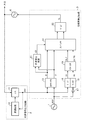
- FIG. FIG. 5 is a block diagram showing a frequency synthesizer according to Embodiment 2 of the present invention.
- the switch 31 is disposed on the output side of the loop filter 15 corresponding to the current output, and is closed when the synchronization detection circuit 21 does not detect the establishment of phase synchronization, and when the synchronization detection circuit 21 detects the establishment of phase synchronization.
- the switch 32 is arranged on the output side of the loop filter 20 corresponding to the voltage output, and is closed when the synchronization detection circuit 21 detects the establishment of phase synchronization, and when the synchronization detection circuit 21 does not detect the establishment of phase synchronization.
- the adder circuit 33 includes a control voltage V t1 (the zero control voltage when the switch 31 is open) that is an output of the first signal path from the D-type flip-flop 13 to the switch 31, and the EX-OR circuit 19. Is added to the control voltage V t2 (zero control voltage when the switch 32 is open), which is the output of the second signal path from to the switch 32, and the control voltage V t after the addition is added to the voltage controlled oscillator. 4 is a circuit that outputs the signal.
- the switches 31 and 32 and the adder circuit 33 constitute control voltage selection means.
- the phase difference detection circuit 3 has one switch 22 mounted. However, the phase difference detection circuit 3 has two switches 31 and 32. The same effects as those of the first embodiment may be obtained. Since operations other than the switches 31 and 32 and the adder circuit 33 are the same as those in the first embodiment, only operations of the switches 31 and 32 and the adder circuit 33 will be described below.
- Switch 31 receives the synchronization signal LD logic low indicating that the synchronization detection circuit 21 is not established phase synchronization is closed, the control voltage V t1 generated by the current output corresponding loop filter 15 adder circuit To 33.
- the circuit is opened, and a zero control voltage V t1 (no signal) is output to the addition circuit 33.
- the switch 32 When the switch 32 receives a logic high synchronization signal LD indicating that phase synchronization is established from the synchronization detection circuit 21, the switch 32 is in a closed state, and adds a control voltage V t2 generated by the voltage output corresponding loop filter 20 to the addition circuit. To 33. On the other hand, when a logic low synchronization signal LD indicating that phase synchronization is not established is received from the synchronization detection circuit 21, the circuit is opened, and a zero control voltage V t2 (no signal) is output to the addition circuit 33.
- the adding circuit 33 adds the control voltage V t1 output from the switch 31 and the control voltage V t2 output from the switch 32, and as shown in the following equation (1), the added control voltage V t Is output to the voltage controlled oscillator 4.
- V t ⁇ ⁇ V t1 + ⁇ ⁇ V t2 (1)
- ⁇ and ⁇ are arbitrary coefficients.
- the control voltage V t1 and the control voltage V t2 are set by setting ⁇ and ⁇ to appropriate values. Can be compensated for.
- the charge pump 14 and the current output corresponding loop filter 15 are mounted in the subsequent stage of the D-type flip-flop 13. As shown, a voltage output-corresponding loop filter 23 for the D-type flip-flop is provided in place of the charge pump 14 and the current output-corresponding loop filter 15 to generate the control voltage V t1. Can play.
- the switch 31 in the first signal path from the D-type flip-flop 13 to the output side of the current output corresponding loop filter 15, the switch 31 is arranged on the output side of the current output corresponding loop filter 15.
- a switch 31 may be disposed between the charge pump 14 and the current output loop filter 15.
- a switch 31 may be disposed between the D-type flip-flop 13 and the charge pump 14.
- a switch 31 may be disposed between the D-type flip-flop 13 and the voltage-type loop filter 23 for the D-type flip-flop.
- the switch 32 in the second signal path from the EX-OR circuit 19 to the output side of the voltage output corresponding loop filter 20, the switch 32 is arranged on the output side of the voltage output corresponding loop filter 20.
- a switch 32 may be disposed between the EX-OR circuit 19 and the voltage output loop filter 20.
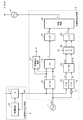
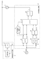
- FIG. 11 is a block diagram showing a frequency synthesizer according to Embodiment 3 of the present invention.
- a phase comparator 41 with a dead zone (denoted as “DZ-PD” in FIG. 11), which is the first phase comparator, is output from the reference signal source 1 in the same manner as the D-type flip-flop 13.
- a process of outputting the phase difference signals D and U corresponding to the phase difference between the reference signal REF and the synchronization signal DIV output from the variable frequency divider 11 to the charge pump 14 is performed.
- the signal in the reference signal REF and the synchronization signal DIV is performed.
- the time difference of the edge detection timing is smaller than a predetermined value, it is different from the D flip-flop 13 in that it has a characteristic of generating a zero phase difference signal.
- the third embodiment is different from the second embodiment in that a phase comparator 41 with a dead zone is provided instead of the D-type flip-flop 13 and the switch 31 is not mounted.
- a phase comparator 41 with a dead zone is provided instead of the D-type flip-flop 13 and the switch 31 is not mounted.
- FIG. 12 is an explanatory diagram showing detection characteristics with respect to a phase difference when using the phase comparator 41 with a dead zone.
- the dead zone-equipped phase comparator 41 has a phase difference corresponding to the phase difference between the reference signal REF output from the reference signal source 1 and the synchronization signal DIV output from the variable frequency divider 11.
- the signals D and U are output to the charge pump 14, but as shown in FIG. 12, when the time difference between the signal edge detection timings in the reference signal REF and the synchronization signal DIV is smaller than a predetermined value, a zero phase difference signal is output. It has the characteristics to generate. That is, as shown in FIG. 12, the phase comparator 41 with a dead zone has a detection output of zero when the phase difference is near zero.
- the switch 32 is arranged on the output side of the voltage output corresponding loop filter 20.
- a switch 32 may be disposed between the EX-OR circuit 19 and the voltage output loop filter 20.
- the phase difference detection circuit 3 is mounted with the charge pump 14 and the current output loop filter 15.
- FIG. 14 and FIG. 3 may be provided with a voltage output corresponding loop filter 23 for the D-type flip-flop.
- FIG. FIG. 16 is a block diagram showing a frequency synthesizer according to Embodiment 4 of the present invention.
- the switch 51 serving as the control voltage selection means selects the phase difference signals D and U generated by the D-type flip-flop 13, and selects the phase difference signal D
- the switch 51 serving as the control voltage selection means selects the phase difference signals D and U generated by the D-type flip-flop 13, and selects the phase difference signal D
- the phase difference signals OUT and OUTB output from the EX-OR circuit 19 are selected and the phase difference is selected.
- a process of outputting the signals OUT and OUTB to the voltage output corresponding loop filter 52 is performed.
- a voltage output corresponding loop filter 52 (indicated as “V-LF” in FIG. 16), which is a control voltage generation circuit, smoothes the phase difference signals D and U or the phase difference signals OUT and OUTB output from the switch 51. as a phased voltage controlled voltage V t, and carries out a process of outputting to the voltage controlled oscillator 4.
- the switch 51 receives a logic low synchronization signal LD indicating that phase synchronization has not been established from the synchronization detection circuit 21
- the switch 51 selects the phase difference signals D and U generated by the D-type flip-flop 13, and The phase difference signals D and U are output to the voltage output corresponding loop filter 52.
- the phase difference signals OUT and OUTB output from the EX-OR circuit 19 are selected and the phase difference is selected.
- the signals OUT and OUTB are output to the voltage output corresponding loop filter 52.
- the voltage output smoothing loop 52 controls the voltage obtained by smoothing the phase difference signals D and U or the phase difference signals OUT and OUTB. as V t, and outputs to the voltage controlled oscillator 4.
- V t the voltage controlled oscillator 4.
- the phase difference detection circuit 3 is mounted with the D-type flip-flop 13.
- the phase difference detection circuit 3 includes the phase comparator 41 with a dead zone. You may make it mount.
- the voltage output loop filter 20 outputs a voltage obtained by smoothing the phase difference signals OUT and OUTB output from the EX-OR circuit 19 as the control voltage V t2 .
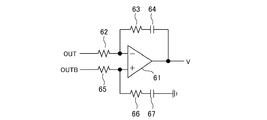
- the voltage output corresponding loop filter 20 includes an operational amplifier 61, resistors 62, 63, 65, 66 and capacitors 64, 67.
- the phase difference signal OUT is input to the inverting input terminal of the operational amplifier 61, and the phase difference signal OUTB that is a differential signal pair of the phase difference signal OUT is input to the non-inverting input terminal of the operational amplifier 61.
- a smoothed difference signal (OUTB ⁇ OUT) is output from the output terminal of the operational amplifier 61 as the control voltage V t2 .
- the voltage output corresponding loop filter 20 includes an operational amplifier 61, resistors 62, 63, 69, a capacitor 64, and an offset DC power supply 68.
- any one of the phase difference signals OUT and OUTB which is a differential signal pair is input to the inverting input terminal of the operational amplifier 61, so that the voltage smoothed from the output terminal of the operational amplifier 61 is controlled.
- the voltage Vt2 is output.
- the DC offset voltage of the phase difference signals OUT and OUTB output from the EX-OR circuit 19 is half of the power supply voltage Vcc of the EX-OR circuit 19. Therefore, in the voltage output-corresponding loop filter 20 of FIG. 19, the offset DC power supply 68 is used to correct the DC offset included in the phase difference signal OUT or the phase difference signal OUTB.
- the voltage output loop filter 20 includes an operational amplifier 61, resistors 62, 63, 69, 70, a capacitor 64, and an offset DC power supply 68.
- any one of the phase difference signals OUT and OUTB that is a differential signal pair is input to the inverting input terminal of the operational amplifier 61, so that the voltage smoothed from the output terminal of the operational amplifier 61 is controlled.
- the voltage Vt2 is output.
- the DC offset included in the phase difference signal OUT or the phase difference signal OUTB is obtained by using the offset DC power source 68 as in the voltage output-corresponding loop filter 20 shown in FIG. It is corrected.
- the frequency synthesizer according to the present invention is applied to, for example, a wireless communication device, and is particularly suitable for a wireless communication device that requires low spurious characteristics.
Landscapes
- Stabilization Of Oscillater, Synchronisation, Frequency Synthesizers (AREA)
Abstract
Priority Applications (4)
| Application Number | Priority Date | Filing Date | Title |
|---|---|---|---|
| PCT/JP2011/002283 WO2012143970A1 (fr) | 2011-04-19 | 2011-04-19 | Synthétiseur de fréquence |
| EP11864036.6A EP2629424A1 (fr) | 2011-04-19 | 2011-04-19 | Synthétiseur de fréquence |
| JP2013510735A JPWO2012143970A1 (ja) | 2011-04-19 | 2011-04-19 | 周波数シンセサイザ |
| US13/882,827 US20130214836A1 (en) | 2011-04-19 | 2011-04-19 | Frequency synthesizer |
Applications Claiming Priority (1)
| Application Number | Priority Date | Filing Date | Title |
|---|---|---|---|
| PCT/JP2011/002283 WO2012143970A1 (fr) | 2011-04-19 | 2011-04-19 | Synthétiseur de fréquence |
Publications (1)
| Publication Number | Publication Date |
|---|---|
| WO2012143970A1 true WO2012143970A1 (fr) | 2012-10-26 |
Family
ID=47041128
Family Applications (1)
| Application Number | Title | Priority Date | Filing Date |
|---|---|---|---|
| PCT/JP2011/002283 Ceased WO2012143970A1 (fr) | 2011-04-19 | 2011-04-19 | Synthétiseur de fréquence |
Country Status (4)
| Country | Link |
|---|---|
| US (1) | US20130214836A1 (fr) |
| EP (1) | EP2629424A1 (fr) |
| JP (1) | JPWO2012143970A1 (fr) |
| WO (1) | WO2012143970A1 (fr) |
Cited By (1)
| Publication number | Priority date | Publication date | Assignee | Title |
|---|---|---|---|---|
| WO2019008672A1 (fr) * | 2017-07-04 | 2019-01-10 | 三菱電機株式会社 | Circuit pll |
Families Citing this family (1)
| Publication number | Priority date | Publication date | Assignee | Title |
|---|---|---|---|---|
| WO2015062663A1 (fr) * | 2013-10-31 | 2015-05-07 | Ecole Polytechnique Federale De Lausanne (Epfl) | Boucle a verrouillage de phase duale et pilotee |
Citations (3)
| Publication number | Priority date | Publication date | Assignee | Title |
|---|---|---|---|---|
| JPH08191247A (ja) * | 1995-01-11 | 1996-07-23 | Matsushita Electric Ind Co Ltd | Pll回路 |
| JP2000059213A (ja) * | 1998-08-12 | 2000-02-25 | Nec Corp | クロック再生装置 |
| JP2001177397A (ja) * | 1999-12-17 | 2001-06-29 | Opnext Japan Inc | 位相周波数同期回路および光受信回路 |
Family Cites Families (15)
| Publication number | Priority date | Publication date | Assignee | Title |
|---|---|---|---|---|
| JPS60109330A (ja) * | 1983-11-17 | 1985-06-14 | Fujitsu Ltd | Pll回路 |
| JPH01243622A (ja) * | 1988-03-25 | 1989-09-28 | Hitachi Ltd | 位相同期ループ回路 |
| US4975650A (en) * | 1989-07-24 | 1990-12-04 | Motorola, Inc. | Phase detector |
| JPH04252519A (ja) * | 1990-12-27 | 1992-09-08 | Nec Corp | 周波数シンセサイザ |
| JPH04256218A (ja) * | 1991-02-08 | 1992-09-10 | Nippon Telegr & Teleph Corp <Ntt> | 低雑音位相同期発振回路 |
| JPH10107624A (ja) * | 1996-10-01 | 1998-04-24 | Sony Corp | Pll回路 |
| JP2001144607A (ja) * | 1999-11-12 | 2001-05-25 | Anritsu Corp | 信号発生器 |
| US6509800B2 (en) * | 2001-04-03 | 2003-01-21 | Agilent Technologies, Inc. | Polyphase noise-shaping fractional-N frequency synthesizer |
| JP4093826B2 (ja) * | 2002-08-27 | 2008-06-04 | 富士通株式会社 | クロック発生装置 |
| JP2004241960A (ja) * | 2003-02-05 | 2004-08-26 | Mitsubishi Electric Corp | 周波数シンセサイザ |
| US7042258B2 (en) * | 2004-04-29 | 2006-05-09 | Agere Systems Inc. | Signal generator with selectable mode control |
| JP2006033414A (ja) * | 2004-07-16 | 2006-02-02 | Yokogawa Electric Corp | 位相同期回路 |
| JP4453753B2 (ja) * | 2007-12-06 | 2010-04-21 | パナソニック電工株式会社 | フラクショナルnpllシンセサイザ、フラクショナルnpllシンセサイザの発振周波数帯域制限方法 |
| JP5284131B2 (ja) * | 2009-02-04 | 2013-09-11 | 株式会社東芝 | 位相同期回路及びこれを用いた受信機 |
| US8446191B2 (en) * | 2009-12-07 | 2013-05-21 | Qualcomm Incorporated | Phase locked loop with digital compensation for analog integration |
-
2011
- 2011-04-19 JP JP2013510735A patent/JPWO2012143970A1/ja active Pending
- 2011-04-19 US US13/882,827 patent/US20130214836A1/en not_active Abandoned
- 2011-04-19 EP EP11864036.6A patent/EP2629424A1/fr not_active Withdrawn
- 2011-04-19 WO PCT/JP2011/002283 patent/WO2012143970A1/fr not_active Ceased
Patent Citations (3)
| Publication number | Priority date | Publication date | Assignee | Title |
|---|---|---|---|---|
| JPH08191247A (ja) * | 1995-01-11 | 1996-07-23 | Matsushita Electric Ind Co Ltd | Pll回路 |
| JP2000059213A (ja) * | 1998-08-12 | 2000-02-25 | Nec Corp | クロック再生装置 |
| JP2001177397A (ja) * | 1999-12-17 | 2001-06-29 | Opnext Japan Inc | 位相周波数同期回路および光受信回路 |
Non-Patent Citations (3)
| Title |
|---|
| KEN'ICHI TAJIMA: "A Low-Noise Fractional-N PLL Synthesizer with DC Offset Adjustment of a Loop Filter", NEN IEICE ELECTRONICS SOCIETY, 17 September 2008 (2008-09-17), TAIKAI KOEN RONBUNSHU 1, pages S-72 - S-73 * |
| TSUNG-HSIEN LIN ET AL.: "Dynamic Current-Matching Charge Pump and Gated-Offset Linearization Technique for Delta-Sigma Fractional-N PLLs", IEEE TRANSACTIONS ON CIRCUITS AND SYSTEMS-I, vol. 56, no. 5, May 2009 (2009-05-01), pages 877 - 885 |
| Y. SUMI ET AL.: "Dead-zone-less PLL Frequency Synthesizer by Hybrid Phase Detectors", PROCEEDINGS OF THE IEEE SYMPOSIUM ON CIRCUITS AND SYSTEMS, vol. 4, June 1999 (1999-06-01), pages 410 - 414 |
Cited By (1)
| Publication number | Priority date | Publication date | Assignee | Title |
|---|---|---|---|---|
| WO2019008672A1 (fr) * | 2017-07-04 | 2019-01-10 | 三菱電機株式会社 | Circuit pll |
Also Published As
| Publication number | Publication date |
|---|---|
| JPWO2012143970A1 (ja) | 2014-07-28 |
| US20130214836A1 (en) | 2013-08-22 |
| EP2629424A1 (fr) | 2013-08-21 |
Similar Documents
| Publication | Publication Date | Title |
|---|---|---|
| CN102843134B (zh) | 具有自动时钟对准的数字pll | |
| US7489757B2 (en) | Clock data recovery circuit | |
| KR100421411B1 (ko) | 클록 신호 재생 장치 | |
| US9019016B2 (en) | Accumulator-type fractional N-PLL synthesizer and control method thereof | |
| WO2012172745A1 (fr) | Système d'annulation de variations brusques de phases au niveau de changements de gain en boucle dans des synthétiseurs de fréquences fractionnaires n | |
| JP2012005124A (ja) | 位相固定ループ及びその動作方法 | |
| JP3670615B2 (ja) | 位相比較器およびクロックリカバリ回路 | |
| US8638141B1 (en) | Phase-locked loop | |
| WO2012143970A1 (fr) | Synthétiseur de fréquence | |
| WO2020012557A1 (fr) | Circuit à boucle à verrouillage de phase | |
| JP6513535B2 (ja) | 自己注入位相同期回路 | |
| CN100353673C (zh) | 锁相环频率合成器 | |
| EP3624344B1 (fr) | Circuit pll | |
| KR20150076825A (ko) | 위상 고정 루프 및 그 제어 방법 | |
| JP2005086789A (ja) | クロックデータリカバリ回路 | |
| JPH11308097A (ja) | 周波数比較器およびこれを用いたpll回路 | |
| JP2005191684A (ja) | クロック生成装置 | |
| JP2000148281A (ja) | クロック選択回路 | |
| CN114499503B (zh) | 一种无中断切换的锁相环电路及电路板组件 | |
| JP2012204883A (ja) | アキュムレータ型フラクショナルn−pllシンセサイザおよびその制御方法 | |
| JP4317821B2 (ja) | 位相ロックループ回路 | |
| JP2972294B2 (ja) | 位相同期回路 | |
| JP2000244311A (ja) | クロック切替調整方法及び回路 | |
| JPH05110428A (ja) | 位相同期回路 | |
| Saifullah et al. | Frequency-to-Voltage Converter Based Dual-Loop PLL with Variable Phase Locking Capability |
Legal Events
| Date | Code | Title | Description |
|---|---|---|---|
| 121 | Ep: the epo has been informed by wipo that ep was designated in this application |
Ref document number: 11864036 Country of ref document: EP Kind code of ref document: A1 |
|
| ENP | Entry into the national phase |
Ref document number: 2013510735 Country of ref document: JP Kind code of ref document: A |
|
| WWE | Wipo information: entry into national phase |
Ref document number: 13882827 Country of ref document: US |
|
| WWE | Wipo information: entry into national phase |
Ref document number: 2011864036 Country of ref document: EP |
|
| NENP | Non-entry into the national phase |
Ref country code: DE |