WO2012144048A1 - Appareil de mesure de grandeurs dynamiques - Google Patents
Appareil de mesure de grandeurs dynamiques Download PDFInfo
- Publication number
- WO2012144048A1 WO2012144048A1 PCT/JP2011/059832 JP2011059832W WO2012144048A1 WO 2012144048 A1 WO2012144048 A1 WO 2012144048A1 JP 2011059832 W JP2011059832 W JP 2011059832W WO 2012144048 A1 WO2012144048 A1 WO 2012144048A1
- Authority
- WO
- WIPO (PCT)
- Prior art keywords
- sensor chip
- notch
- mechanical quantity
- measuring device
- quantity measuring
- Prior art date
- Legal status (The legal status is an assumption and is not a legal conclusion. Google has not performed a legal analysis and makes no representation as to the accuracy of the status listed.)
- Ceased
Links
Images







Classifications
-
- G—PHYSICS
- G01—MEASURING; TESTING
- G01B—MEASURING LENGTH, THICKNESS OR SIMILAR LINEAR DIMENSIONS; MEASURING ANGLES; MEASURING AREAS; MEASURING IRREGULARITIES OF SURFACES OR CONTOURS
- G01B7/00—Measuring arrangements characterised by the use of electric or magnetic techniques
- G01B7/16—Measuring arrangements characterised by the use of electric or magnetic techniques for measuring the deformation in a solid, e.g. by resistance strain gauge
-
- G—PHYSICS
- G01—MEASURING; TESTING
- G01L—MEASURING FORCE, STRESS, TORQUE, WORK, MECHANICAL POWER, MECHANICAL EFFICIENCY, OR FLUID PRESSURE
- G01L1/00—Measuring force or stress, in general
- G01L1/18—Measuring force or stress, in general using properties of piezo-resistive materials, i.e. materials of which the ohmic resistance varies according to changes in magnitude or direction of force applied to the material
-
- G—PHYSICS
- G01—MEASURING; TESTING
- G01L—MEASURING FORCE, STRESS, TORQUE, WORK, MECHANICAL POWER, MECHANICAL EFFICIENCY, OR FLUID PRESSURE
- G01L1/00—Measuring force or stress, in general
- G01L1/26—Auxiliary measures taken, or devices used, in connection with the measurement of force, e.g. for preventing influence of transverse components of force, for preventing overload
-
- H—ELECTRICITY
- H10—SEMICONDUCTOR DEVICES; ELECTRIC SOLID-STATE DEVICES NOT OTHERWISE PROVIDED FOR
- H10D—INORGANIC ELECTRIC SEMICONDUCTOR DEVICES
- H10D48/00—Individual devices not covered by groups H10D1/00 - H10D44/00
- H10D48/50—Devices controlled by mechanical forces, e.g. pressure
-
- G—PHYSICS
- G01—MEASURING; TESTING
- G01L—MEASURING FORCE, STRESS, TORQUE, WORK, MECHANICAL POWER, MECHANICAL EFFICIENCY, OR FLUID PRESSURE
- G01L19/00—Details of, or accessories for, apparatus for measuring steady or quasi-steady pressure of a fluent medium insofar as such details or accessories are not special to particular types of pressure gauges
- G01L19/14—Housings
- G01L19/147—Details about the mounting of the sensor to support or covering means
Definitions
- the present invention relates to a mechanical quantity measuring device in which a sensor chip is supported on a flexible wiring board.
- the mechanical quantity measuring device can measure a mechanical quantity that is attached to the object to be measured and acts on the object to be measured.
- a device using a sensor chip to which an effect of changing resistance depending on strain (piezoresistance effect) is applied has been proposed.
- the sensor chip has an impurity diffusion resistor formed on the surface thereof, and the sensor chip is attached to an object to be measured with an adhesive.
- the impurity diffusion resistance is distorted and the resistance changes via the adhesive, so this change in resistance can be output as a sense output.
- a mechanical quantity (strain) acting on an object can be detected.
- the sense output may fluctuate with time.
- an object of the present invention is to provide a mechanical quantity measuring device capable of suppressing the temporal variation of the sense output.
- the present invention provides a sensor chip that outputs a sense output corresponding to a mechanical quantity acting on the object to be measured, and a wiring that supports the sensor chip and extracts the sense output to the outside.
- the mechanical quantity measuring device comprising the flexible wiring board, and in the measurement of the mechanical quantity, the sensor chip and the flexible wiring board are attached to the object to be measured.
- a notch is provided in the flexible wiring board in the vicinity of the sensor chip and on the side where the wiring is arranged with respect to the sensor chip.
- FIG. 1 is a plan view of a mechanical quantity measuring device according to a first embodiment of the present invention. It is a bottom view of the mechanical quantity measuring device which concerns on the 1st Embodiment of this invention.
- 1B is an enlarged view of FIG. 1A around the sensor chip of the mechanical quantity measuring device according to the first embodiment of the present invention.
- FIG. It is a top view when the mechanical quantity measuring apparatus which concerns on the 1st Embodiment of this invention is affixed on the to-be-measured object with the adhesive agent.
- FIG. 4 is an enlarged view of a cross-sectional view taken along the line AA in FIG. 3. It is a top view of an example (the 1) of a sensor chip. It is a top view of an example (the 2) of a sensor chip.
- FIG. 4 is a schematic diagram of a cross section taken along the line AA in FIG. 3. It is an enlarged view around a sensor chip of a mechanical quantity measuring device concerning a 2nd embodiment of the present invention. It is a top view of the mechanical quantity measuring apparatus which concerns on the 3rd Embodiment of this invention.
- FIG. 11 is an enlarged view of FIG. 10 around a sensor chip of a mechanical quantity measuring device according to a third embodiment of the present invention.
- FIG. 10 is a cross-sectional view taken along the line BB in FIG. 10 when the mechanical quantity measuring device around the sensor chip of the mechanical quantity measuring device according to the third embodiment of the present invention is attached to an object to be measured with an adhesive.
- FIG. 11 is a schematic cross-sectional view corresponding to the cross section taken along the line AA in FIG. 10 when the mechanical quantity measuring device according to the third embodiment of the present invention is attached to an object to be measured with an adhesive.
- FIG. 16 is an enlarged view of FIG. 15 around a sensor chip of a mechanical quantity measuring device according to a fourth embodiment of the present invention.
- constituent elements are not necessarily indispensable except for the case where they are clearly indicated and the case where they are clearly considered to be essential in principle.
- constituent elements and the like when “consisting of A”, “consisting of A”, “having A”, and “including A” are specifically indicated that only those elements are included. It goes without saying that other elements are not excluded except in the case of such cases.
- the shapes, positional relationships, etc. of the components, etc. when referring to the shapes, positional relationships, etc. of the components, etc., the shapes are substantially the same unless otherwise specified, or otherwise apparent in principle. And the like are included. The same applies to the above numerical values and ranges.
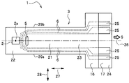
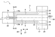
- FIG. 1A shows a plan view of a mechanical quantity measuring device 1 according to the first embodiment of the present invention.
- the mechanical quantity measuring device 1 includes a sensor chip 2 and a flexible wiring board 3 that supports the sensor chip 2.
- the sensor chip 2 can output a sense output S corresponding to a mechanical quantity acting on the device under test 4 (see FIG. 3).
- the flexible wiring board 3 includes a wiring 6 and an external electrode 25 that is electrically connected to the wiring 6.
- the wiring 6 is electrically connected to the sensor chip 2 and extracts the sense output S from the sensor chip 2.
- the external electrode 25 outputs the sense output S from the wiring 6 to the outside.
- the flexible wiring board 3 has an arm part 21 and a base part 24 connected to the arm part 21.
- the arm portion 21 supports the sensor chip 2 at the distal end portion 22 and is connected to the base portion 24 at the base portion 23.
- the wiring 6 is drawn from the tip 22 of the arm 21 to the root 23.
- An external electrode 25 connected to the wiring 6 is provided on the base 24.
- the flexible wiring board 3 is used in many semiconductor mounting products by taking advantage of its excellent flexibility.
- the thickness can be reduced to 100 ⁇ m or less and the wiring portion can be reduced in size, which is an essential component for portable electronic devices.
- the flexible wiring board 3 is provided with a notch (slit) 5.
- the notch (slit) 5 is provided in the flexible wiring board 3 between the sensor chip 2 and the external electrode 25.
- the notch (slit) 5 is provided in the flexible wiring board 3 in the vicinity of the sensor chip 2 and on the side where the wiring 6 is disposed with respect to the sensor chip 2.
- the notch 5 is provided on the external electrode 25 side with respect to the sensor chip 2 in the longitudinal direction 27 of the arm portion 21 in the direction from the distal end portion 22 of the arm portion 21 to the root portion 23.
- the longitudinal direction 28 of the notch 5 intersects the longitudinal direction 27 of the arm portion 21 at a substantially right angle.
- the longitudinal direction 28 of the notch 5 intersects the center line 26 of the arm portion 21 parallel to the longitudinal direction 27 of the arm portion 21 at a substantially right angle.
- the notch 5 can be produced by punching using a press die, as in the case of producing the outer shape of the flexible wiring board 3, so that it does not cause an increase in cost.
- the sensor chip 2 is arranged so that the center point 2a is on the center line 26 of the arm portion 21.
- the sensor chip 2 is arranged so as to be line symmetric with respect to the center line 26 of the arm portion 21.
- a plurality of wirings 6 (four in the example of FIG. 1A) are drawn.
- the plurality of wirings 6 are routed so as to bypass the notch 5.
- the plurality of wirings 6 are arranged so as to be symmetrical with respect to each other about the center line 26 of the arm portion 21 as an axis.
- the base film 17 is exposed over almost the entire surface on the surface side of the mechanical quantity measuring device 1 (flexible wiring board 3).
- FIG. 1B shows a bottom view of the mechanical quantity measuring device 1 according to the first embodiment of the present invention.
- the sensor chip 2 is supported on the back side of the flexible wiring board 3.
- the wiring 6 is formed under the base film 17 and is further covered with an insulating film 16. That is, the wiring 6 is covered with the base film 17 from the front surface side of the flexible wiring substrate 3 and is covered with the insulating film 16 from the back surface side of the flexible wiring substrate 3.
- the external electrode 25 is formed under the base film 17. The lower side of the external electrode 25 is not covered with the insulating film 16 and is exposed so that it can be connected to an external device.
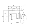
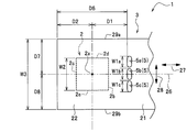
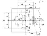
- FIG. 2 shows an enlarged view around the sensor chip 2 of the mechanical quantity measuring device 1 according to the first embodiment of the present invention.
- Both ends in the longitudinal direction 28 of the notch 5 have an arc shape.
- the notch 5 is symmetric with respect to a center line 26 parallel to the longitudinal direction 27 of the arm portion 21.
- the width W1 of the notch 5 in the direction that intersects the longitudinal direction 27 of the arm portion 21 at a substantially right angle is divided into two equal parts by the center line 26 of the arm portion 21.
- the width W1 of the notch 5 in the direction intersecting with the longitudinal direction 27 of the arm portion 21 at a substantially right angle is compared with the width W2 of the direction intersecting with the longitudinal direction 27 of the arm portion 21 of the sensor chip 2 at a substantially right angle.
- the center point 2 a of the sensor chip 2 is disposed on a center line 26 parallel to the longitudinal direction 27 of the arm portion 21.
- the sensor chip 2 has a substantially square shape in plan view.
- the side 2b is disposed so as to face the notch 5.
- the side 2c is arranged in parallel so as to face the end side of the arm portion 21 on the distal end portion 22 side.
- the side 2 d is arranged in parallel so as to face the side side 29 a along the longitudinal direction 27 of the arm portion 21 of the flexible wiring board 3.
- the side 2 e is arranged in parallel so as to face the side side 29 b along the longitudinal direction 27 of the arm portion 21 of the flexible wiring board 3.
- the side 2b facing the notch 5 of the sensor chip 2 intersects the center line 26 of the arm portion 21 at a substantially right angle.
- the longitudinal direction 28 of the notch 5 intersects the longitudinal direction 27 (center line 26) of the arm portion 21 at a substantially right angle.
- the longitudinal direction 28 of the notch 5 is arrange
- a distance D1 from the notch 5 to the center point 2a of the sensor chip 2 is a distance D2 from the side opposite to the notch 5 to the sensor chip 2 of the flexible wiring board 3 to the center point 2a of the sensor chip 2.
- D1 D2
- the distance D1 from the notch 5 to the center point 2a of the sensor chip 2 is a distance D7 from the side edge 29a to the center point 2a of the sensor chip 2 and a distance D8 from the side edge 29b to the center point 2a of the sensor chip 2.
- the sensor chip 2 has a square shape in plan view.
- the present invention is not limited thereto, and the sensor chip 2 may be rectangular or circular as long as the center point 2a can be determined.
- FIG. 3 shows a state in which the mechanical quantity measuring device 1 according to the first embodiment of the present invention is attached to the object to be measured 4 with the adhesive 7.
- the sensor chip 2 and the flexible wiring board 3 are attached to the object to be measured 4 with an adhesive 7 when measuring the mechanical quantity.
- the adhesive 7 is applied not only from the sensor chip 2 and the tip 22 of the arm 21 around the sensor chip 2 but also from the tip 22 of the arm 21 to the vicinity of the root 23.
- the bonding end surface 7 c of the adhesive 7 reaches the vicinity of the base portion 23 of the arm portion 21.
- the adhesive 7 is not applied to the base 24 of the flexible wiring board 3.
- the adhesive 7 may be a two-component or one-component adhesive made of an epoxy resin.
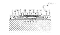
- FIG. 4 is an enlarged view of the main part of the cross-sectional view taken along the arrow AA in FIG.
- a plurality of electrode pads (chip side) 12 are formed on the surface of the sensor chip 2.
- a plurality of electrode pads (flexible wiring board side) 15 are formed on the back surface of the base film 17 facing the plurality of electrode pads 12.
- the plurality of electrode pads 15 are connected to the wiring 6.
- the electrode pad (chip side) 12 and the electrode pad (flexible wiring board side) 15 are connected by a bump 13 such as a gold bump.
- An area other than the bumps 13 between the sensor chip 2 and the flexible wiring board 3 is filled with an underfill material 14.
- the sensor chip 2 is attached to and supported by the flexible wiring board 3 by the bumps 13 and particularly the underfill material 14.
- an epoxy resin can be used, short circuit prevention between the bumps 13 and between the electrode pads 12 and 15, protection of the surface of the sensor chip 2, and bonding force between the flexible wiring board 3 and the sensor chip 2. It is used for the purpose of enhancement.
- the flexible wiring board 3 In the flexible wiring board 3, wiring 6 is formed on the back surface of the base film 17, and an insulating film 16 is formed under the wiring 6.
- the flexible wiring board 3 has a sandwich structure in which the wiring 6 is sandwiched between the base film 17 and the insulating film 16.
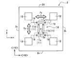
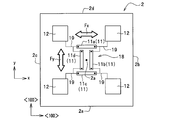
- FIG. 5A shows a plan view of an example (part 1) of the sensor chip 2.
- a semiconductor substrate in particular, a silicon (Si) single crystal substrate having a (100) surface can be used.
- piezoresistive elements 11 (11a, 11b, 11c, 11d) are formed on the sensor chip 2 (semiconductor substrate).
- the piezoresistive element 11 is an impurity diffused resistor formed on the surface of the semiconductor substrate.
- the conductivity type of the piezoresistive element (impurity diffused resistor) 11 is p-type. In the piezoresistive element 11, the direction of current flow is the longitudinal direction of the piezoresistive element 11.
- the longitudinal direction of the piezoresistive element 11 is the ⁇ 110> direction of the crystal orientation of the semiconductor substrate.
- the longitudinal direction of the piezoresistive element 11 (11a, 11c) is the x-axis direction (direction parallel to the sides 2d, 2e).
- the longitudinal direction of the piezoresistive element 11 (11b, 11d) is the y-axis direction (direction parallel to the sides 2b, 2c) perpendicular to the x-axis direction.
- the four piezoresistive elements 11 (11a, 11b, 11c, 11d) are connected by an in-chip wiring 19, and a Wheatstone bridge circuit 18 is formed.
- Four electrode pads (chip side) 12 are connected to the intra-chip wiring 19. According to such a sensor chip 2, a sense output S corresponding to a difference in mechanical quantity between a strain (mechanical quantity) Fx in the x direction and a strain (dynamic quantity) Fy in the y direction is output with high sensitivity. Can do.
- an amplifier circuit can be formed on the surface of the sensor chip 2 on which the Wheatstone bridge circuit 18 is formed. Since the Wheatstone bridge circuit 18 and the amplifier circuit formed on the sensor chip can all be manufactured using a normal semiconductor manufacturing process, miniaturization is easy and manufacturing cost can be reduced.
- the sensor chip 2 outputs a sense output S corresponding to the difference in mechanical quantity between the strain (mechanical quantity) Fx in the x direction and the strain (dynamic quantity) Fy in the y direction. Even if a thermal strain that changes and depends on the difference in linear expansion coefficient between the sensor chip 2 and the DUT 4 is generated, the thermal strain becomes a uniform value in the x-direction and the y-direction, and can be canceled. . That is, if the sensor chip 2 is used, there is no need to worry about variations in strain values due to changes in environmental temperature.
- the size of the typical adhesion region 7b is the same in the x direction and the y direction of the sensor chip 2. Since the stress to be relaxed is the same in the x direction and the y direction of the sensor chip 2, the stress to be relaxed can be canceled in the same manner as the change in the environmental temperature.
- FIG. 5B shows a plan view of an example (part 2) of the sensor chip 2.
- An example (part 2) of the sensor chip 2 is different from an example (part 1) of the sensor chip 2 in that the conductivity type of the piezoresistive element (impurity diffused resistor) 11 is an n-type. . Accordingly, the longitudinal direction of the piezoresistive element 11 is the ⁇ 100> direction of the crystal orientation of the semiconductor substrate. Even with such a sensor chip 2, it is possible to output the sense output S corresponding to the difference in mechanical quantity between the strain (mechanical quantity) Fx in the x direction and the strain (dynamic quantity) Fy in the y direction with high sensitivity. it can.
- FIG. 6 shows a cross-sectional view of a conventional mechanical quantity measuring device.
- the inventors of the present application show that the reason that the sense output fluctuates with time in the conventional mechanical quantity measuring device is that the strain generated in the flexible wiring board 3 is relaxed with time. Revealed.
- tensile strain is generated in the device under test 4
- tensile strain is also generated in the flexible wiring substrate 3 attached to the device under test 4, and stress is generated.
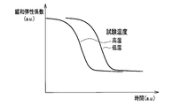
- the flexible wiring board 3 is formed with resin materials, such as a polyimide and an epoxy resin, and when the test which loads a fixed strain with respect to a resin material (flexible wiring board 3) was performed, with progress of time, resin Stress relaxation occurs so that the stress generated in the material (flexible wiring board 3) is reduced.
- FIG. 7 shows the change over time of the relaxation elastic modulus of the resin material (flexible wiring board 3). It can be seen that the relaxation elastic modulus decreases with time. Regardless of the time, even if a constant tensile strain is generated in the flexible wiring board 3, if the relaxation elastic modulus decreases, the stress that is the product of the tensile strain (amount) and the relaxation elastic modulus decreases. Relaxation occurs. Note that the relaxation elastic modulus decreases earlier as the test temperature (the temperature of the resin material) becomes higher.
- the strain state of the measurement object 4 to which the flexible wiring board 3 is attached changes, and the flexible wiring board 3
- the strain state of the sensor chip 2 supported by and attached to the object to be measured 4 changes. That is, the sense output S of the sensor chip 2 varies due to the stress relaxation of the flexible wiring board 3.
- the variation amount of the sense output S increases as the bonding area 7a of the adhesive 7 that bonds the flexible wiring board 3 and the DUT 4 increases.
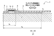
- FIG. 8 schematically shows a cross-sectional view taken along the line AA in FIG.
- the size of the adhesive region 7a of the adhesive 7 that adheres the flexible wiring board 3 and the object to be measured 4 is the same as that of the conventional mechanical quantity measuring apparatus.
- the adhesion region where the sense output S is varied is substantially the adhesion region 7b, which is considered to be smaller than the conventional one. Thereby, the fluctuation
- the tension acts on the sensor chip 2 by bypassing the flexible wiring board 3 instead of being straight, so that the influence of the tension on the sensor chip 2 can be suppressed.
- the notch 5 is provided, the size of the adhesive region 7a of the adhesive 7 that adheres the flexible wiring board 3 and the object 4 to be measured is hardly reduced as compared with the conventional case.
- the wiring board 3 is not peeled off, and connection reliability can be ensured. Further, since the adhesive 7 is fixed on the side wall of the flexible wiring board 3 in the notch 5, the flexible wiring board 3 can be firmly bonded to the object to be measured 4 by the so-called anchor effect.
- the size of the region 7b is the same in the x direction and the y direction (see FIG. 5A) of the sensor chip 2. Since the relaxing stress is equal in the x direction and the y direction of the sensor chip 2, it is possible to output the sense output S in which the relaxing stress is canceled.
- FIG. 9 shows an enlarged view around the sensor chip 2 of the mechanical quantity measuring device 1 according to the second embodiment of the present invention.
- the mechanical quantity measuring device 1 according to the second embodiment is different from the mechanical quantity measuring device 1 according to the first embodiment in that the notch 5 is divided into a plurality of parts.
- FIG. 9 shows an example in which the notch 5 is divided into three notches 5a, 5b, and 5c. Both ends of the cutouts 5a, 5b, and 5c in the longitudinal direction 28 have an arc shape.
- the notches 5 a, 5 b, 5 c are arranged in a line in the longitudinal direction 28 of the notch 5.
- the longitudinal direction of the notches 5 a, 5 b, 5 c substantially coincides with the longitudinal direction 28 of the notch 5.
- the notches 5 (5a, 5b, 5c) are line symmetric with respect to a center line 26 parallel to the longitudinal direction 27 of the arm portion 21.
- the notch 5b is line-symmetric with the center line 26 as an axis.
- a width W1b in a direction that intersects the longitudinal direction 27 of the arm portion 21 of the notch 5b at a substantially right angle is divided into two equal parts by the center line 26.
- the notch 5a and the notch 5c are line symmetric with respect to the center line 26 as an axis.
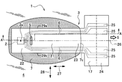
- FIG. 10 shows a plan view of a mechanical quantity measuring device 1 according to the third embodiment of the present invention.
- the mechanical quantity measuring device 1 according to the third embodiment is different from the mechanical quantity measuring device 1 according to the first embodiment in that, in addition to the notch 5, the first separate notch 51 and the second separate notch 52 and the third separate notch 53 are provided in the flexible wiring board 3.
- the first separate cutout 51 is provided on the opposite side of the cutout 5 with respect to the sensor chip 2 of the flexible wiring board 3. With respect to the sensor chip 2, the notch 5 is disposed on one side of the arm portion 21 in the longitudinal direction 27, and the first separate notch 51 is disposed on the other side.
- the second separate cutout 52 is provided between the sensor chip 2 and one side 29a of two opposite sides along the longitudinal direction 27 of the arm portion 21 of the flexible wiring board 3.
- the third separate cutout 53 is provided between the sensor chip 2 and the other side 29b of the two opposite sides along the longitudinal direction 27 of the arm portion 21 of the flexible wiring board 3.
- a second separate notch 52 is disposed on one side of the sensor chip 2 in a direction perpendicular to the longitudinal direction 27 of the arm portion 21, and a third separate notch 53 is disposed on the other side.
- FIG. 11 shows a state around the sensor chip 2 of the mechanical quantity measuring device 1 according to the third embodiment of the present invention.
- the notch 5 faces the side 2 b of the sensor chip 2.
- the longitudinal direction of the notch 5 is substantially parallel to the side 2b.
- the width W1 in the longitudinal direction of the notch 5 is substantially equal to or larger than the length (width) W2 of the side 2b (W1 ⁇ W2).
- the first separate cutout 51 faces the side 2c of the sensor chip 2.
- the longitudinal direction of the first separate cutout 51 is substantially parallel to the side 2c.
- the second separate notch 52 faces the side 2d of the sensor chip 2.
- the longitudinal direction of the second separate notch 52 is substantially parallel to the side 2d.
- the third separate notch 53 faces the side 2e of the sensor chip 2.
- the longitudinal direction of the third separate notch 53 is substantially parallel to the side 2e.
- FIG. 12 corresponds to the cross section taken along the line AA in FIG.
- the first separate cutout 51 is provided on the opposite side of the cutout 5 with respect to the sensor chip 2 of the flexible wiring board 3.
- the notch 5 is disposed on one side of the arm portion 21 in the longitudinal direction 27, and the first separate notch 51 is disposed on the other side. Since the sensor chip 2 is provided with the notches 5 and 51 on both sides, the symmetry is enhanced and the stress acting on the sensor chip 2 from the flexible wiring board 3 can be made uniform.
- the adhesive 7 is fixed on the side wall of the flexible wiring board 3, so that the sensor chip 2 is supported by the so-called anchor effect from both sides.
- the flexible wiring board 3 can be firmly and uniformly bonded to the object 4 to be measured.
- FIG. 13 is a cross-sectional view when the mechanical quantity measuring device 1 around the sensor chip 2 of the mechanical quantity measuring device 1 according to the third embodiment of the present invention is attached to the measurement object 4 with the adhesive 7.
- . 13 corresponds to the cross section taken along the line BB in FIG.
- a second separate notch 52 is disposed on one side of the sensor chip 2 in a direction perpendicular to the longitudinal direction 27 of the arm portion 21, and a third separate notch 53 is disposed on the other side. Since the sensor chip 2 is provided with the notches 52 and 53 on both sides, the symmetry is enhanced, and the stress acting on the sensor chip 2 from the flexible wiring board 3 can be made uniform.
- the adhesive 7 is fixed on the side wall of the flexible wiring board 3, so that the sensor chip 2 is supported by the so-called anchor effect from both sides.
- the flexible wiring board 3 at the position can be firmly and uniformly bonded to the object to be measured 4.
- FIG. 14 schematically shows a cross-sectional view when the mechanical quantity measuring device 1 according to the third embodiment of the present invention is attached to the object to be measured 4 with the adhesive 7.
- 14 corresponds to the cross section taken along the line AA in FIG.
- the size of the adhesive region 7a of the adhesive 7 that adheres the flexible wiring board 3 and the measured object 4 is the same as that of the conventional mechanical quantity measuring device (see FIG. 6).
- the cutout 5 and the first separate cutout 51 are provided, the bonding region that varies the sense output S is substantially the bonding region 7b. It is thought that it is smaller than the conventional one.
- the cutout 5 and the first separate cutout 51 can be easily brought close to the sensor chip 2 without reducing the bonding area 7a.
- the substantial adhesion region 7b for changing the sense output S can be made smaller than that in the first embodiment.
- FIG. 15 shows a plan view of a mechanical quantity measuring device 1 according to the fourth embodiment of the present invention
- FIG. 16 shows an enlarged view around the sensor chip 2 of the mechanical quantity measuring device 1.
- the notch 5 is divided into a plurality of parts, similarly to the mechanical quantity measuring device 1 according to the second embodiment.
- the mechanical quantity measuring device 1 according to the fourth embodiment is different from the mechanical quantity measuring device 1 according to the second embodiment in that the divided notches 5a and 5c are on the side of the flexible wiring board 3. This is a point that reaches the sides 29a and 29b. It can be considered that this point is cut from the side edges 29a and 29b, and the notches 5a and 5c are formed in the side edges 29a and 29b.
- the notches 5a and 5c in the longitudinal direction 28 has an arc shape.
- the notches 5 a and 5 c are arranged in a line along the longitudinal direction 28 of the notch 5.
- the longitudinal direction of the notches 5 a and 5 c is substantially coincident with the longitudinal direction 28 of the notch 5.
- the notches 5a and 5c are symmetrical with respect to each other about a center line 26 parallel to the longitudinal direction 27 of the arm portion 21.
- the wiring 6 (see FIG. 1A) can pass between the notch 5a and the notch 5c without detouring the notch 5, so that the wiring 6 is similar to the second embodiment.
- the degree of freedom in design can be improved.
Landscapes
- Physics & Mathematics (AREA)
- General Physics & Mathematics (AREA)
- Pressure Sensors (AREA)
- Force Measurement Appropriate To Specific Purposes (AREA)
- Measurement Of Length, Angles, Or The Like Using Electric Or Magnetic Means (AREA)
Abstract
Priority Applications (5)
| Application Number | Priority Date | Filing Date | Title |
|---|---|---|---|
| JP2013510791A JPWO2012144048A1 (ja) | 2011-04-21 | 2011-04-21 | 力学量測定装置 |
| US14/110,716 US9190537B2 (en) | 2011-04-21 | 2011-04-21 | Mechanical quantity measuring device |
| EP11864095.2A EP2703770A4 (fr) | 2011-04-21 | 2011-04-21 | Appareil de mesure de grandeurs dynamiques |
| PCT/JP2011/059832 WO2012144048A1 (fr) | 2011-04-21 | 2011-04-21 | Appareil de mesure de grandeurs dynamiques |
| KR1020137027306A KR20140020963A (ko) | 2011-04-21 | 2011-04-21 | 역학량 측정 장치 |
Applications Claiming Priority (1)
| Application Number | Priority Date | Filing Date | Title |
|---|---|---|---|
| PCT/JP2011/059832 WO2012144048A1 (fr) | 2011-04-21 | 2011-04-21 | Appareil de mesure de grandeurs dynamiques |
Publications (1)
| Publication Number | Publication Date |
|---|---|
| WO2012144048A1 true WO2012144048A1 (fr) | 2012-10-26 |
Family
ID=47041197
Family Applications (1)
| Application Number | Title | Priority Date | Filing Date |
|---|---|---|---|
| PCT/JP2011/059832 Ceased WO2012144048A1 (fr) | 2011-04-21 | 2011-04-21 | Appareil de mesure de grandeurs dynamiques |
Country Status (5)
| Country | Link |
|---|---|
| US (1) | US9190537B2 (fr) |
| EP (1) | EP2703770A4 (fr) |
| JP (1) | JPWO2012144048A1 (fr) |
| KR (1) | KR20140020963A (fr) |
| WO (1) | WO2012144048A1 (fr) |
Cited By (1)
| Publication number | Priority date | Publication date | Assignee | Title |
|---|---|---|---|---|
| EP2746004B1 (fr) * | 2012-12-19 | 2018-03-07 | Weber Maschinenbau GmbH Breidenbach | Procédé et dispositif de découpe de produits alimentaires avec détermination de la force de coupe |
Families Citing this family (7)
| Publication number | Priority date | Publication date | Assignee | Title |
|---|---|---|---|---|
| EP2796830B1 (fr) * | 2011-12-06 | 2019-03-13 | Hitachi, Ltd. | Dispositif de mesure de déformation |
| JP6293982B2 (ja) * | 2015-09-30 | 2018-03-14 | 日立オートモティブシステムズ株式会社 | 力学量測定装置 |
| JP6704126B2 (ja) * | 2015-12-17 | 2020-06-03 | パナソニックIpマネジメント株式会社 | 接続構造体 |
| US20180272540A1 (en) * | 2017-03-24 | 2018-09-27 | Panasonic Intellectual Property Management Co., Ltd. | Resort sanitation monitor and controller |
| US10217366B2 (en) | 2017-03-29 | 2019-02-26 | Panasonic Intellectual Property Management Co., Ltd. | Autonomous resort sanitation |
| DE102019129411A1 (de) * | 2019-09-12 | 2021-03-18 | Wika Alexander Wiegand Se & Co. Kg | Aufnehmerkörper mit einem Messelement und Herstellungsverfahren für einen Aufnehmerkörper |
| JP2021071305A (ja) * | 2019-10-29 | 2021-05-06 | ミネベアミツミ株式会社 | 力覚センサ装置 |
Citations (4)
| Publication number | Priority date | Publication date | Assignee | Title |
|---|---|---|---|---|
| JPH06174564A (ja) * | 1992-12-03 | 1994-06-24 | Ishida Co Ltd | 計量装置のロードセル |
| JP2001264188A (ja) | 2000-03-21 | 2001-09-26 | Olympus Optical Co Ltd | 半導体歪ゲージおよび半導体歪ゲージの製造方法 |
| JP2002139389A (ja) * | 2000-10-30 | 2002-05-17 | Nagano Keiki Co Ltd | 荷重測定用センシング素子 |
| JP2009264976A (ja) * | 2008-04-25 | 2009-11-12 | Hitachi Metals Ltd | 半導体歪センサー |
Family Cites Families (10)
| Publication number | Priority date | Publication date | Assignee | Title |
|---|---|---|---|---|
| JPH0719978A (ja) * | 1993-06-23 | 1995-01-20 | Matsushita Refrig Co Ltd | 圧力センサ |
| ATE222010T1 (de) * | 1998-05-19 | 2002-08-15 | Infineon Technologies Ag | Sensoreinrichtung zur erfassung von biometrischen merkmalen, insbesondere fingerminutien |
| US20030001250A1 (en) * | 2001-06-27 | 2003-01-02 | Walsin Advanced Electronics Ltd | TCP optical device |
| US20030042587A1 (en) * | 2001-08-31 | 2003-03-06 | Tsung-Jen Lee | IC packaging and manufacturing methods |
| DE10335690A1 (de) * | 2003-06-04 | 2004-12-23 | Sensor-Technik Wiedemann Gmbh | Verformungssensor |
| JP4617943B2 (ja) * | 2005-03-18 | 2011-01-26 | 株式会社日立製作所 | 力学量測定装置 |
| JP4379360B2 (ja) * | 2005-03-22 | 2009-12-09 | 株式会社日立製作所 | 力学量測定装置 |
| TW200730997A (en) * | 2006-02-10 | 2007-08-16 | Asia Optical Co Inc | Camera module |
| US20070241895A1 (en) * | 2006-04-13 | 2007-10-18 | Morgan Kelvin L | Noise reduction for flexible sensor material in occupant detection |
| US7843021B2 (en) * | 2008-02-28 | 2010-11-30 | Shandong Gettop Acoustic Co. Ltd. | Double-side mountable MEMS package |
-
2011
- 2011-04-21 WO PCT/JP2011/059832 patent/WO2012144048A1/fr not_active Ceased
- 2011-04-21 EP EP11864095.2A patent/EP2703770A4/fr not_active Withdrawn
- 2011-04-21 KR KR1020137027306A patent/KR20140020963A/ko not_active Ceased
- 2011-04-21 JP JP2013510791A patent/JPWO2012144048A1/ja active Pending
- 2011-04-21 US US14/110,716 patent/US9190537B2/en active Active
Patent Citations (4)
| Publication number | Priority date | Publication date | Assignee | Title |
|---|---|---|---|---|
| JPH06174564A (ja) * | 1992-12-03 | 1994-06-24 | Ishida Co Ltd | 計量装置のロードセル |
| JP2001264188A (ja) | 2000-03-21 | 2001-09-26 | Olympus Optical Co Ltd | 半導体歪ゲージおよび半導体歪ゲージの製造方法 |
| JP2002139389A (ja) * | 2000-10-30 | 2002-05-17 | Nagano Keiki Co Ltd | 荷重測定用センシング素子 |
| JP2009264976A (ja) * | 2008-04-25 | 2009-11-12 | Hitachi Metals Ltd | 半導体歪センサー |
Non-Patent Citations (1)
| Title |
|---|
| See also references of EP2703770A4 |
Cited By (2)
| Publication number | Priority date | Publication date | Assignee | Title |
|---|---|---|---|---|
| EP2746004B1 (fr) * | 2012-12-19 | 2018-03-07 | Weber Maschinenbau GmbH Breidenbach | Procédé et dispositif de découpe de produits alimentaires avec détermination de la force de coupe |
| US10179419B2 (en) | 2012-12-19 | 2019-01-15 | Weber Maschinenbau Gmbh Breidenbach | Method and food slicing device with cutting force determination |
Also Published As
| Publication number | Publication date |
|---|---|
| EP2703770A4 (fr) | 2014-11-12 |
| JPWO2012144048A1 (ja) | 2014-07-28 |
| US9190537B2 (en) | 2015-11-17 |
| KR20140020963A (ko) | 2014-02-19 |
| US20140027868A1 (en) | 2014-01-30 |
| EP2703770A1 (fr) | 2014-03-05 |
Similar Documents
| Publication | Publication Date | Title |
|---|---|---|
| WO2012144048A1 (fr) | Appareil de mesure de grandeurs dynamiques | |
| TWI390205B (zh) | 加速度感測器 | |
| JP5779662B2 (ja) | 力学量測定装置 | |
| JP6293982B2 (ja) | 力学量測定装置 | |
| EP2184576B1 (fr) | Capteur de déformation à semi-conducteur | |
| CN105765360B (zh) | 压力传感器 | |
| US20150276517A1 (en) | Mechanical Quantity Measuring Device | |
| JP6216879B2 (ja) | トルク検出装置 | |
| CN110160681B (zh) | 负荷感测装置、封装件以及系统 | |
| JP2006258674A (ja) | 力学量測定装置 | |
| JP2014048072A (ja) | 圧力センサモジュール | |
| JP7526032B2 (ja) | ひずみセンサモジュール | |
| JP2015017848A (ja) | 力学量測定装置 | |
| JP2025093752A (ja) | 重量計 | |
| JP4816065B2 (ja) | センサモジュールの製造方法 | |
| JP2015094646A (ja) | 力学量測定装置 |
Legal Events
| Date | Code | Title | Description |
|---|---|---|---|
| 121 | Ep: the epo has been informed by wipo that ep was designated in this application |
Ref document number: 11864095 Country of ref document: EP Kind code of ref document: A1 |
|
| ENP | Entry into the national phase |
Ref document number: 2013510791 Country of ref document: JP Kind code of ref document: A |
|
| WWE | Wipo information: entry into national phase |
Ref document number: 14110716 Country of ref document: US |
|
| ENP | Entry into the national phase |
Ref document number: 20137027306 Country of ref document: KR Kind code of ref document: A |
|
| NENP | Non-entry into the national phase |
Ref country code: DE |
|
| WWE | Wipo information: entry into national phase |
Ref document number: 2011864095 Country of ref document: EP |