WO2012144126A1 - 発光装置、バックライトユニット、液晶表示装置及び照明装置 - Google Patents
発光装置、バックライトユニット、液晶表示装置及び照明装置 Download PDFInfo
- Publication number
- WO2012144126A1 WO2012144126A1 PCT/JP2012/001698 JP2012001698W WO2012144126A1 WO 2012144126 A1 WO2012144126 A1 WO 2012144126A1 JP 2012001698 W JP2012001698 W JP 2012001698W WO 2012144126 A1 WO2012144126 A1 WO 2012144126A1
- Authority
- WO
- WIPO (PCT)
- Prior art keywords
- light emitting
- emitting device
- sealing member
- substrate
- present
- Prior art date
- Legal status (The legal status is an assumption and is not a legal conclusion. Google has not performed a legal analysis and makes no representation as to the accuracy of the status listed.)
- Ceased
Links
Images










Classifications
-
- H—ELECTRICITY
- H10—SEMICONDUCTOR DEVICES; ELECTRIC SOLID-STATE DEVICES NOT OTHERWISE PROVIDED FOR
- H10H—INORGANIC LIGHT-EMITTING SEMICONDUCTOR DEVICES HAVING POTENTIAL BARRIERS
- H10H20/00—Individual inorganic light-emitting semiconductor devices having potential barriers, e.g. light-emitting diodes [LED]
- H10H20/80—Constructional details
- H10H20/85—Packages
- H10H20/851—Wavelength conversion means
- H10H20/8515—Wavelength conversion means not being in contact with the bodies
-
- G—PHYSICS
- G02—OPTICS
- G02F—OPTICAL DEVICES OR ARRANGEMENTS FOR THE CONTROL OF LIGHT BY MODIFICATION OF THE OPTICAL PROPERTIES OF THE MEDIA OF THE ELEMENTS INVOLVED THEREIN; NON-LINEAR OPTICS; FREQUENCY-CHANGING OF LIGHT; OPTICAL LOGIC ELEMENTS; OPTICAL ANALOGUE/DIGITAL CONVERTERS
- G02F1/00—Devices or arrangements for the control of the intensity, colour, phase, polarisation or direction of light arriving from an independent light source, e.g. switching, gating or modulating; Non-linear optics
- G02F1/01—Devices or arrangements for the control of the intensity, colour, phase, polarisation or direction of light arriving from an independent light source, e.g. switching, gating or modulating; Non-linear optics for the control of the intensity, phase, polarisation or colour
- G02F1/13—Devices or arrangements for the control of the intensity, colour, phase, polarisation or direction of light arriving from an independent light source, e.g. switching, gating or modulating; Non-linear optics for the control of the intensity, phase, polarisation or colour based on liquid crystals, e.g. single liquid crystal display cells
- G02F1/133—Constructional arrangements; Operation of liquid crystal cells; Circuit arrangements
- G02F1/1333—Constructional arrangements; Manufacturing methods
- G02F1/1335—Structural association of cells with optical devices, e.g. polarisers or reflectors
- G02F1/1336—Illuminating devices
- G02F1/133615—Edge-illuminating devices, i.e. illuminating from the side
-
- H—ELECTRICITY
- H10—SEMICONDUCTOR DEVICES; ELECTRIC SOLID-STATE DEVICES NOT OTHERWISE PROVIDED FOR
- H10H—INORGANIC LIGHT-EMITTING SEMICONDUCTOR DEVICES HAVING POTENTIAL BARRIERS
- H10H20/00—Individual inorganic light-emitting semiconductor devices having potential barriers, e.g. light-emitting diodes [LED]
- H10H20/80—Constructional details
- H10H20/85—Packages
- H10H20/852—Encapsulations
-
- H—ELECTRICITY
- H10—SEMICONDUCTOR DEVICES; ELECTRIC SOLID-STATE DEVICES NOT OTHERWISE PROVIDED FOR
- H10H—INORGANIC LIGHT-EMITTING SEMICONDUCTOR DEVICES HAVING POTENTIAL BARRIERS
- H10H20/00—Individual inorganic light-emitting semiconductor devices having potential barriers, e.g. light-emitting diodes [LED]
- H10H20/80—Constructional details
- H10H20/85—Packages
- H10H20/857—Interconnections, e.g. lead-frames, bond wires or solder balls
-
- H—ELECTRICITY
- H10—SEMICONDUCTOR DEVICES; ELECTRIC SOLID-STATE DEVICES NOT OTHERWISE PROVIDED FOR
- H10H—INORGANIC LIGHT-EMITTING SEMICONDUCTOR DEVICES HAVING POTENTIAL BARRIERS
- H10H29/00—Integrated devices, or assemblies of multiple devices, comprising at least one light-emitting semiconductor element covered by group H10H20/00
- H10H29/10—Integrated devices comprising at least one light-emitting semiconductor component covered by group H10H20/00
- H10H29/14—Integrated devices comprising at least one light-emitting semiconductor component covered by group H10H20/00 comprising multiple light-emitting semiconductor components
-
- H—ELECTRICITY
- H10—SEMICONDUCTOR DEVICES; ELECTRIC SOLID-STATE DEVICES NOT OTHERWISE PROVIDED FOR
- H10W—GENERIC PACKAGES, INTERCONNECTIONS, CONNECTORS OR OTHER CONSTRUCTIONAL DETAILS OF DEVICES COVERED BY CLASS H10
- H10W90/00—Package configurations
-
- H—ELECTRICITY
- H10—SEMICONDUCTOR DEVICES; ELECTRIC SOLID-STATE DEVICES NOT OTHERWISE PROVIDED FOR
- H10H—INORGANIC LIGHT-EMITTING SEMICONDUCTOR DEVICES HAVING POTENTIAL BARRIERS
- H10H20/00—Individual inorganic light-emitting semiconductor devices having potential barriers, e.g. light-emitting diodes [LED]
- H10H20/01—Manufacture or treatment
- H10H20/032—Manufacture or treatment of electrodes
-
- H—ELECTRICITY
- H10—SEMICONDUCTOR DEVICES; ELECTRIC SOLID-STATE DEVICES NOT OTHERWISE PROVIDED FOR
- H10H—INORGANIC LIGHT-EMITTING SEMICONDUCTOR DEVICES HAVING POTENTIAL BARRIERS
- H10H20/00—Individual inorganic light-emitting semiconductor devices having potential barriers, e.g. light-emitting diodes [LED]
- H10H20/01—Manufacture or treatment
- H10H20/036—Manufacture or treatment of packages
- H10H20/0361—Manufacture or treatment of packages of wavelength conversion means
-
- H—ELECTRICITY
- H10—SEMICONDUCTOR DEVICES; ELECTRIC SOLID-STATE DEVICES NOT OTHERWISE PROVIDED FOR
- H10H—INORGANIC LIGHT-EMITTING SEMICONDUCTOR DEVICES HAVING POTENTIAL BARRIERS
- H10H20/00—Individual inorganic light-emitting semiconductor devices having potential barriers, e.g. light-emitting diodes [LED]
- H10H20/01—Manufacture or treatment
- H10H20/036—Manufacture or treatment of packages
- H10H20/0362—Manufacture or treatment of packages of encapsulations
-
- H—ELECTRICITY
- H10—SEMICONDUCTOR DEVICES; ELECTRIC SOLID-STATE DEVICES NOT OTHERWISE PROVIDED FOR
- H10H—INORGANIC LIGHT-EMITTING SEMICONDUCTOR DEVICES HAVING POTENTIAL BARRIERS
- H10H20/00—Individual inorganic light-emitting semiconductor devices having potential barriers, e.g. light-emitting diodes [LED]
- H10H20/01—Manufacture or treatment
- H10H20/036—Manufacture or treatment of packages
- H10H20/0364—Manufacture or treatment of packages of interconnections
-
- H—ELECTRICITY
- H10—SEMICONDUCTOR DEVICES; ELECTRIC SOLID-STATE DEVICES NOT OTHERWISE PROVIDED FOR
- H10H—INORGANIC LIGHT-EMITTING SEMICONDUCTOR DEVICES HAVING POTENTIAL BARRIERS
- H10H20/00—Individual inorganic light-emitting semiconductor devices having potential barriers, e.g. light-emitting diodes [LED]
- H10H20/80—Constructional details
- H10H20/85—Packages
- H10H20/851—Wavelength conversion means
-
- H—ELECTRICITY
- H10—SEMICONDUCTOR DEVICES; ELECTRIC SOLID-STATE DEVICES NOT OTHERWISE PROVIDED FOR
- H10H—INORGANIC LIGHT-EMITTING SEMICONDUCTOR DEVICES HAVING POTENTIAL BARRIERS
- H10H20/00—Individual inorganic light-emitting semiconductor devices having potential barriers, e.g. light-emitting diodes [LED]
- H10H20/80—Constructional details
- H10H20/85—Packages
- H10H20/852—Encapsulations
- H10H20/853—Encapsulations characterised by their shape
Definitions
- the present invention relates to a light emitting device, a backlight unit, a liquid crystal display device, and a lighting device, and more particularly to a light emitting device using a semiconductor light emitting element.
- LEDs light emitting diodes
- the LED is unitized as a light emitting device (light emitting module).
- Patent Document 1 discloses an SMD type light emitting device used for an edge light type backlight unit.
- FIG. 17A is a plan view of a conventional SMD type light emitting device.
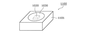
- FIG. 17B is a perspective view of an SMD type LED element used in a conventional SMD type light emitting device.
- the conventional SMD type light emitting device 1000 includes a substrate 1010 and a plurality of SMD type LED elements 1100 mounted on the substrate 1010 in a row.
- each SMD-type LED element 1100 is a package-type LED element, and covers the cavity 1101 molded of resin or the like, the LED 1020 mounted in the cavity 1101, and the LED 1020 And a sealing member 1030 made of a phosphor-containing resin sealed in the cavity 1101.
- the sense of crushing refers to the appearance displayability, and refers to the extent to which a plurality of LED light sources arranged in a row can be independently confirmed when the appearance is confirmed by visual observation or the like.
- the present invention has been made to solve such a problem, and it is an object of the present invention to provide a light emitting device and the like capable of suppressing a luminance variation and suppressing a chromaticity variation while reducing a crushing feeling. Do.
- one aspect of a light emitting device is a long substrate, and a plurality of semiconductor light emitting elements arranged in a straight line along the longitudinal direction of the substrate on the substrate.
- a sealing member including a light wavelength converter and sealing the plurality of semiconductor light emitting devices, wherein the sealing member collectively seals the plurality of semiconductor light emitting devices and the plurality of semiconductor light emitting devices. It is formed linearly along the arrangement direction of the elements.
- the length in the linear direction of the sealing member is Ls and the line width of the sealing member is Ws, 10 ⁇ Ls / Ws. Is preferred.
- the line width of the sealing member can be narrowed, even when the pitch of the semiconductor light emitting device is large, the light of the semiconductor light emitting device reflected at the interface between the sealing member and the air layer is adjacent to each other. It can be advanced between semiconductor light emitting devices. Thereby, the crushing feeling can be further suppressed.
- the length in the linear direction of the semiconductor light emitting element is Lc and the length in the direction orthogonal to the linear direction of the semiconductor light emitting element is Wc It is preferable that it is Lc.
- the luminous flux of the light emitting device can be improved, and the luminance can be improved.
- the cross-sectional shape of the sealing member can be made substantially semicircular, it is possible to suppress uneven brightness and uneven chromaticity regardless of the angle at which the light emitting device (light source) is viewed.
- the height of the sealing member is Hs and the length in the 45 degree direction from the center of the sealing member in the cross section of the sealing member is Hs 45 It is preferable that 9 ⁇ Hs 45 /Hs ⁇ 1.1. Furthermore, in one embodiment of the light emitting device according to the present invention, it is preferable that 0.4 ⁇ Hs / Ws ⁇ 0.6.
- the cross-sectional shape of the sealing member can be made semicircular, it is possible to suppress luminance unevenness and chromaticity unevenness regardless of the angle at which the light emitting device (light source) is viewed.
- the light emitting device further includes two electrodes formed on the substrate for supplying power to the plurality of semiconductor light emitting elements, one of the two electrodes being The other electrode of the two electrodes is formed at the other end of the substrate in the longitudinal direction, and the other electrode of the two electrodes is formed at the other end of the substrate in the longitudinal direction.
- the electrode is formed to be offset to one long side of the substrate with reference to the sealing member.
- the sealing member is formed so that a straight line passing through the center of the line width of the sealing member and a straight line passing through the center in the short direction of the substrate are different. Is preferred.
- the sealing member is preferably formed to both end edges in the longitudinal direction of the substrate.
- the plurality of semiconductor light emitting elements are arranged at the same pitch, and each of the two semiconductor light emitting elements located at both ends of the plurality of semiconductor light emitting elements is It is preferable that the distance between the semiconductor light emitting element located at the both ends and the edge of the substrate be half the pitch.
- a wire is bonded to each of the plurality of semiconductor light emitting elements, and at least a part of each of the wires is sealed by the sealing member.
- all of the wires sealed in the sealing member are provided in the same direction as the linear direction of the sealing member.
- a protective element for electrostatically protecting the plurality of semiconductor light emitting elements is provided, and the protective elements are arranged in a straight line with the plurality of semiconductor light emitting elements. Is preferred.
- the protective element and the plurality of semiconductor light emitting elements are arranged at the same pitch.
- the outline of the end portion of the sealing member has a curvature.
- a wire is bonded to each of the protective element and the plurality of semiconductor light emitting elements, and at least a part of each of the wires is sealed by the sealing member.
- all the wires sealed in the sealing member are provided in the same direction as the linear direction of the sealing member.
- the light emitting device further includes a first wiring and a second wiring electrically connected to the plurality of semiconductor light emitting elements, each of the first wiring and the second wiring being the
- the sealing member has a straight linear portion formed substantially parallel along the longitudinal direction of the substrate on the substrate, and the sealing member is disposed between the linear portion of the first wiring and the linear portion of the second wiring.
- it is formed in
- the linear portion of the first wiring and the linear portion of the second wiring be glass-coated.
- the light wavelength converter is a phosphor that excites light emitted by the plurality of semiconductor light emitting elements.
- one aspect of the backlight unit according to the present invention is provided with the above-described light emitting device.
- the backlight unit it is preferable that a plurality of the light emitting devices be provided, and the plurality of light emitting devices be disposed in contact with the substrates of the light emitting device.
- one aspect of a liquid crystal display device includes the above-described backlight unit, and a liquid crystal panel disposed on a light path of light emitted from the backlight unit.
- one aspect of a lighting device according to the present invention includes the above-described light emitting device.
- the lighting device it is preferable that a plurality of the light emitting devices be provided, and the plurality of light emitting devices be arranged with the substrates of the light emitting device in contact.
- the light emitting device of the present invention it is possible to reduce the feeling of crushing to suppress the luminance variation and to suppress the chromaticity variation.
- FIG. 1 is a schematic perspective view of a light emitting device according to a first embodiment of the present invention.
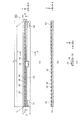
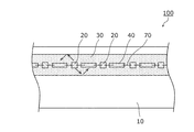
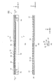
- A) of FIG. 2 is a plan view of the light emitting device according to the first embodiment of the present invention, and (b) of FIG. 2 is a cross-sectional view taken along line XX ′ of (a).
- FIG. 2 (c) is a cross-sectional view taken along the line YY 'of FIG. 2 (a).
- FIG. 3 is an enlarged plan view of the light emitting device according to the first embodiment of the present invention.
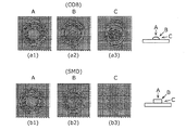
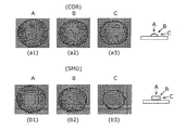
- FIG. 4A is a view showing luminance characteristics of the light emitting device (COB) according to the first embodiment of the present invention and the conventional light emitting device (SMD).
- COB luminance characteristics of the light emitting device
- SMD conventional light emitting device
- FIG. 4B is a diagram showing chromaticity characteristics ( ⁇ x) of the light emitting device (COB) according to the first embodiment of the present invention and the conventional light emitting device (SMD).
- (A) of FIG. 5 is a partially enlarged plan view of the light emitting device according to the first embodiment of the present invention, and (b) of FIG. 5 is an enlarged cross sectional view of the same light emitting device.
- FIG. 6 is a view showing a state in which a plurality of light emitting devices according to the first embodiment of the present invention are arranged.
- FIG. 7 is an enlarged plan view of a connection portion when a plurality of light emitting devices according to the first embodiment of the present invention are arranged, and (b) of FIG. 7 is a side view thereof.
- FIG. 8A is a plan view for illustrating the method for forming the sealing member in the light emitting device according to the first embodiment of the present invention.
- FIG. 8B is a side view (side view of FIG. 8A) for explaining the method of forming the sealing member in the light emitting device according to the first embodiment of the present invention.
- FIG. 8C is a cross-sectional view for explaining a method of forming a sealing member in the light emitting device according to the first embodiment of the present invention (cross-sectional view of FIG. 8A).
- (A) of FIG. 9 is a plan view of a light emitting device according to a second embodiment of the present invention, and
- (b) of FIG. 9 is a cross-sectional view taken along line XX ′ of (a) FIG.
- FIG. 9 (c) is a cross-sectional view taken along the line YY 'of FIG. 9 (a).
- FIG. 10 is a circuit diagram of a light emitting device according to a second embodiment of the present invention.
- FIG. 11 is a view showing a wiring pattern in the light emitting device according to the second embodiment of the present invention.
- FIG. 12A is a plan view for illustrating the method of forming the sealing member in the light emitting device according to the second embodiment of the present invention.
- FIG. 12B is a side view (side view of FIG. 12A) for explaining the method of forming the sealing member in the light emitting device according to the second embodiment of the present invention.
- FIG. 12A is a plan view for illustrating the method of forming the sealing member in the light emitting device according to the second embodiment of the present invention.
- FIG. 12B is a side view (side view of FIG. 12A) for explaining the method of forming the sealing member in the light emitting device according to the second embodiment of the present
- FIG. 12C is a cross-sectional view for explaining a method of forming a sealing member in a light emitting device according to a second embodiment of the present invention (cross-sectional view of FIG. 12A).
- FIG. 13 is an exploded perspective view of a backlight unit according to a third embodiment of the present invention.
- FIG. 14 is a cross-sectional view of a liquid crystal display device according to a fourth embodiment of the present invention.
- FIG. 15 is a partially cutaway perspective view of a lighting device according to a fifth embodiment of the present invention.
- FIG. 16 is a schematic perspective view of a lighting device according to a sixth embodiment of the present invention.
- FIG. 17A is a plan view of a conventional SMD type light emitting device.
- FIG. 17B is a perspective view of an SMD type LED element used in a conventional SMD type light emitting device.
- the X axis, the Y axis, and the Z axis are three axes orthogonal to each other, and in the present embodiment, the X axis direction is the longitudinal direction of the substrate and the Y axis direction is orthogonal to the X axis
- the Z-axis direction is a direction orthogonal to the X-axis and the Y-axis. In the drawings, the dimensions do not exactly match.
- FIG. 1 is a schematic perspective view of a light emitting device according to a first embodiment of the present invention.
- the light emitting device 100 is a linear light source that emits light in a linear shape (linear shape), and a predetermined light source formed on the substrate 10 in a linear shape. And a light emitting unit 110 that emits light.
- the light emitting unit 110 is configured of a plurality of LED chips arranged in a line (one dimension) and a sealing member including a phosphor.
- the light emitting device 100 is a COB (Chip On Board) light emitting device in which an LED chip (bare chip) directly mounted on the substrate 10 is sealed with a phosphor-containing resin.
- COB Chip On Board
- FIG. 2A is a plan view of the light emitting device according to the first embodiment of the present invention.
- FIG. 2B is a cross-sectional view (a cross section in the longitudinal direction of the substrate) of the light emitting device according to the first embodiment of the present invention cut along the line XX ′ in FIG. 2C is a cross-sectional view (a cross-sectional view in the short direction of the substrate) of the light emitting device according to the first embodiment of the present invention cut along the YY ′ line in (a).
- the light emitting device 100 is an LED module (light emitting module) in which a plurality of LED chips are modularized, and a substrate 10 and a plurality of LEDs 20; A sealing member 30, a wire 40, a protection element 50, a first electrode 61 and a second electrode 62, and a wire 70 are provided.
- LED module light emitting module
- a sealing member 30, a wire 40, a protection element 50, a first electrode 61 and a second electrode 62, and a wire 70 are provided.
- each component of the light emitting device 100 will be described in detail.
- the substrate 10 is a mounting substrate for mounting the LED 20, and is a long rectangular substrate.
- the aspect ratio L1 / L2 of the substrate 10 is preferably 10 ⁇ L1 / L2.
- a ceramic substrate made of alumina or translucent aluminum nitride, an aluminum substrate made of an aluminum alloy, a transparent glass substrate, a flexible flexible substrate (FPC) made of a resin, or the like can be used.
- a metal base substrate such as an aluminum substrate
- an insulating film made of an organic material such as polyimide is formed on the substrate 10.
- a white resist material may be formed on the substrate 10.
- the substrate 10 a ceramic substrate made of rectangular alumina having L1 of 140 mm, L2 of 5.5 mm, and a thickness of 1.0 mm was used. Moreover, L1 can be 280 mm and the long board
- the plurality of LEDs 20 is an example of a semiconductor light emitting device, and is mounted directly on the substrate 10.
- the plurality of LEDs 20 are arranged in a line (straight line) along the longitudinal direction of the substrate 10.
- the twenty-four LEDs 20 are arranged in only one row.
- Each LED 20 can use a bare chip that emits monochromatic visible light, and is die-bonded onto the substrate 10 by a die attach material (die bonding material).
- a blue LED chip that emits blue light is used.
- the blue LED chip for example, a gallium nitride-based semiconductor light emitting device having a center wavelength of 440 nm to 470 nm, which is made of an InGaN-based material, can be used.
- a square blue LED chip having a side length of 346 ⁇ m is used as the LED 20, but a rectangular LED chip can also be used.
- the 24 LEDs 20 are arranged at the same pitch, and are configured such that distances between adjacent LEDs 20 are all the same.
- each of the two LEDs 20 located at both ends of the LEDs 20 arranged in a row is arranged such that the distance between the LEDs 20 located at both ends and the short side edge of the substrate 10 is half the pitch of the LEDs 20 It is done. That is, the distance between the LEDs 20 located at the top and the tail of the row and the short side edge of the substrate 10 closest to the LEDs 20 is half the pitch of the LEDs 20 (1/2 pitch).
- the pitch of the LEDs 20 is 5.85 mm.
- the sealing member 30 is a phosphor-containing resin containing a phosphor which is a light wavelength converter, and converts the wavelength of light from the LEDs 20 and simultaneously seals all the LEDs 20 on the substrate 10 to protect the LEDs 20. Do.
- the sealing member 30 is formed on the substrate 10 in a straight line along the arrangement direction of the LEDs 20.
- the linear (stripe-like) sealing member 30 further includes a straight line in the linear direction (stripe direction) passing through the center of the line width (stripe width) of the sealing member 30 and the lateral direction of the substrate 10. It is formed to be different from a straight line passing through the center of (a line connecting centers of opposing short sides). Specifically, as shown in (a) of FIG. 2, the sealing member 30 is formed closer to one long side than a straight line passing the center of the substrate 10 in the short direction.
- the sealing member 30 is formed up to the vicinity of both end edges in the longitudinal direction of the substrate 10. That is, the sealing member 30 is formed without interruption from the end face of one short side of the substrate 10 to the end face of the other short side facing the substrate 10 (see FIG. 1).
- the sealing member 30 for example, when the LED 20 is a blue LED, phosphor-containing yellow phosphor particles of YAG (yttrium aluminum garnet) type dispersed in silicone resin to obtain white light Resin can be used. Further, in the present embodiment, the sealing member 30 is formed so that the length in the linear direction is 140 mm, the line width is 1.5 mm, and the maximum center height is 0.6 mm.
- YAG yttrium aluminum garnet
- a blue LED chip is used as the LED 20, and a phosphor-containing resin containing yellow phosphor particles is used as the sealing member 30.
- the yellow phosphor particles are excited by the blue light of the blue LED chip to emit yellow light. Therefore, from the sealing member 30 (the light emitting unit 110), the excited yellow light and the blue light of the blue LED chip Emits white light.
- the wiring 40 is formed of a conductive member, and is pattern-formed in a predetermined shape to electrically connect the plurality of LEDs 20 with each other. Furthermore, the wiring 40 is also patterned in a predetermined shape in order to electrically connect the plurality of LEDs 20 and the protection element 50. The wiring 40 is electrically connected to the first electrode 61 and the second electrode 62.
- the wiring 40 is formed such that all the LEDs 20 are connected in series. Further, metal wiring such as tungsten (W) or copper (Cu) can be used as the wiring 40, and the surface thereof is coated with a plating made of gold (Au) or the like.
- the protection element 50 is an electrostatic protection element for electrostatically protecting the LED 20, and one or more are mounted on the substrate 10.
- the protection element 50 prevents the LED 20 having a low reverse withstand voltage from being destroyed by static electricity of reverse polarity generated on the substrate 10. For this reason, the protection element 50 is provided so that it may become parallel connection in reverse polarity with LED20.
- a zener diode or the like is used as the protective element 50, and in the present embodiment, one zener diode is provided on the substrate 10.
- the first electrode 61 and the second electrode 62 are electrode terminals (feed parts) for connecting to the external power supply of the light emitting device 100, and are electrically connected to the wiring 40.
- the first electrode 61 and the second electrode 62 are electrode terminals (feed parts) for connecting to the external power supply of the light emitting device 100, and are electrically connected to the wiring 40.
- power is supplied to each LED 20 through the wiring 40 and the wire 70.
- DC current can be supplied to each LED 20.
- the LED 20 emits light, and the desired light is emitted from the LED 20.
- the first electrode 61 and the second electrode 62 are made of gold (Au).
- the first electrode 61 and the second electrode 62 are disposed to face each other on both short sides. That is, the first electrode 61 is formed at one end (one short side end) of the substrate 10 in the longitudinal direction, and the second electrode 62 is formed at the other end of the substrate 10 in the longitudinal direction ( The other short side end portion is formed.
- first electrode 61 and the second electrode 62 are offset to one long side of the substrate 10 with reference to the sealing member 30. That is, the first electrode 61 and the sealing member 30 are formed side by side in the short direction of the substrate 10, and the second electrode 62 is the first electrode 61 of the sealing member 30 based on the sealing member 30. It is formed on the side formed.
- the wire 70 is a wire for electrically connecting the LED 20 and the wire 40, and is made of, for example, a gold wire.
- a p-side electrode and an n-side electrode for supplying current are formed on the top surface of the chip of the LED 20, and the p-side electrode and the n-side electrode are wire-bonded to the wiring 40 by the wire 70.
- the wire 70 is entirely embedded in the sealing member 30. However, when reducing the sealing member 30 to improve the light extraction efficiency, a portion of the wire 70 is exposed from the sealing member 30. There is also a case. Thus, at least a portion of the wire 70 is sealed by the sealing member 30.
- all the wires 70 sealed in the sealing member 30 are provided in the same direction as the linear direction of the sealing member 30. That is, all the wires 70 connected to the LED 20 are provided so as to be on a straight line in plan view.
- FIG. 3 is an enlarged plan view of the light emitting device according to the first embodiment of the present invention.
- the sealing member 30 (phosphor-containing resin) for collectively sealing the LEDs 20 is formed linearly along the arrangement direction of the LEDs 20 .
- the sealing member 30 exists also between adjacent LED20, a non-light-emission area
- region does not exist between adjacent LED20. That is, as shown in FIG. 3, a part of the light emitted from the LED 20 is reflected at the interface with the air layer in the line width direction of the sealing member 30 and travels into the sealing member 30, so the sealing member The light in the 30 linear directions (longitudinal direction of the substrate 10) can be increased. Therefore, since it can be set as a light emission area also between adjacent LEDs 20, there is an effect that the feeling of crushing can be eliminated and the luminance variation can be suppressed.
- the linear length of the sealing member 30 (the length in the longitudinal direction of the substrate 10 in the sealing member 30) is Ls
- the line width of the sealing member 30 (the width of the substrate 10 in the sealing member 30)
- Ls and Ws may be appropriately determined in accordance with the shape of a desired light emitting device, but it is preferable that 10 ⁇ Ls / Ws. More preferably, 30 ⁇ Ls / Ws is preferable.
- an elongated linear sealing member 30 with a long stripe length and a narrow stripe width can do.
- L1 of the substrate 10 is 140 mm
- L1 of the substrate 10 is 280 mm
- the sealing member 30 can be elongated to narrow the line width, the sealing member 30 and the air layer can be obtained even when the pitch of the LEDs 20 is large.
- the light of the LED 20 reflected at the interface with the light travels between the adjacent LEDs 20. As a result, the crushing feeling can be further reduced.
- the sealing member 30 has a linear shape, a crushing feeling occurs if the line width is large or the pitch of the LEDs is large.
- a crushing feeling can be suppressed by adjusting the linear shape of the sealing member 30 suitably in the said range.
- the sealing member 30 for collectively sealing the LEDs 20 is formed linearly along the arrangement direction of the LEDs 20, the sealing member 30 is not disconnected in the module. As a result, it is also possible to suppress the chromaticity difference in the module caused by the internal diffusion. In particular, it is possible to suppress color unevenness in the central portion that most achieves the light emitting function.
- the light emitting device 100 According to the light emitting device 100 according to the first embodiment of the present invention, it is possible to reduce the feeling of crushing and suppress the luminance non-uniformity (luminance non-uniformity) and the color non-uniformity (chromaticity non-uniformity).
- FIG. 4A is a view showing luminance characteristics of the light emitting device (COB) according to the first embodiment of the present invention and the conventional light emitting device (SMD).
- FIG. 4B is a diagram showing chromaticity characteristics ( ⁇ x) of the light emitting device (COB) according to the first embodiment of the present invention and the conventional light emitting device (SMD).
- the characteristics of (a1) and (b1), the characteristics of (a2) and (b2), and the characteristics of (c1) and (c1) are the A direction, the B direction, and the C direction, respectively. It shows the results when measured from the direction.
- the pitch of LED of the light-emitting device (COB) which concerns on this embodiment, and the conventional light-emitting device (SMD) is substantially the same.
- the luminance variation is large among the A direction, the B direction, and the C direction.
- the luminance is significantly reduced compared to when viewed from the A direction and the B direction.
- the variation in luminance among the directions A, B, and C is small.
- luminance variation can be suppressed.
- the variation in the thickness of the wall surface of the cavity portion occurs due to the inclination of mounting of the LED (SMD) and the dicing variation, so the luminance variation of side emission becomes large.
- the light emitting device (COB) even in side light emission, there is no variation in luminance and uniform luminance is obtained. That is, the light emitting device (COB) according to the present embodiment can reduce the feeling of crushing feeling at the angle at which the light emitting device (light source) is viewed, as compared with the conventional light emitting device (SMD).
- the chromaticity difference between each direction of A direction, B direction and C direction is small.
- the chromaticity variation can be suppressed.
- the light emitting device 100 According to the light emitting device 100 according to the present embodiment, it is possible to suppress uneven brightness (uneven luminance) and suppress uneven color (uneven chromaticity).
- FIG. (A) of FIG. 5 is a partially enlarged plan view of the light emitting device according to the first embodiment of the present invention, and (b) of FIG. 5 is an enlarged cross sectional view of the same light emitting device.
- the length (length of the LED chip) of the LED 20 (LED chip) in the X-axis direction (longitudinal direction of the substrate 10) is Lc
- the substrate 10 of the LED 20 (LED chip) Assuming that the length in the Y-axis direction (the width of the LED chip) is Wc, it is preferable to set Wc ⁇ Lc. Thereby, the luminous flux of the light emitting device 100 can be improved, and the luminance can be improved. In the case of Wc ⁇ Lc, it was found that the luminous flux is improved by 3% as compared with the case of Wc> Lc.
- the length of the substrate 10 of the sealing member 30 in the Y-axis direction is Ws
- Wc Ws / 4.
- the distance between the chip centers of the LEDs 20 is preferably 6 mm or less. In terms of the distance between the chip edges of the LED 20, the distance between the chip edges is preferably 5.5 mm or less.
- the line width of the sealing member 30 is Ws
- the height of the sealing member 30 is Hs
- the length (thickness) of the direction is Hs 45
- the cross-sectional shape of the sealing member 30 can be made substantially semicircular, so that uneven brightness and uneven chromaticity can be suppressed regardless of the angle at which the light emitting device 100 (light source) is viewed.
- the sealing member 30 is formed in a straight line with the LEDs 20 arranged in a straight line.
- the state of the sealing member 30 formed so as to surround the LEDs 20 is stable with the same configuration regardless of which LED 20 is at the center. Therefore, even if color unevenness occurs, periodic color unevenness occurs, and stable light emission can be obtained without causing a large discomfort.
- the sealing members are formed discontinuously in one module, when the modules are used side by side, a difference in chromaticity occurs between the modules, or color unevenness in the lateral direction occurs.
- the first electrode 61 and the second electrode 62 are formed to be offset to one long side of the substrate 10 with reference to the sealing member 30. .
- the width (length of the short side) of the substrate 10 can be reduced compared to the case of the both sides arrangement. it can.
- an elongated linear light emitting module can be realized, and the cost can be suppressed.
- all the wires 70 sealed in the sealing member 30 are provided in the same direction as the linear direction of the sealing member 30. Thereby, the sealing member 30 can be formed in a stable shape.
- the sealing member 30 when forming the sealing member 30, the sealing member material is pulled in the wiring direction of the wire 70 when the sealing member material is applied. Therefore, when the wiring direction of the wire 70 is different from the linear direction of the sealing member 30, the sealing member 30 may not be able to be formed into a good linear shape (stripe shape). For example, in some parts of the sealing member 30, portions with different line widths may occur and the line widths may not be constant. On the other hand, by making the wiring direction of the wire 70 the same as the linear direction of the sealing member 30, the sealing member material is pulled only in the linear direction when the sealing member material is applied. Thus, the sealing member 30 having a uniform line width can be easily formed.
- the light emitting device 100 according to the first embodiment is very useful when a very long light source such as a straight tube type LED lamp equivalent to 1200 mm is required.
- the sealing members 30 are formed to the vicinity of both end edges in the longitudinal direction of the substrate 10 as shown as the light emitting portion 110 in FIG. Therefore, when a plurality of these are connected, it is possible to configure a state in which the sealing members 30 of the adjacent light emitting devices 100 are connected without a gap.
- a linear light source in which a plurality of light emitting units are connected can be obtained, and as described above, it is possible to obtain a linear light source exceeding 1000 mm.
- the method of connecting the plurality of light emitting devices 100 is not particularly limited.
- a wiring is disposed in a region of the substrate where the sealing member 30 is not formed, and a method of connecting with each other by a bridge structure of the wirings, or a single long plate member is prepared,
- the method of connecting the plurality of light emitting devices 100 is not particularly limited, as long as it is a method capable of mechanically and electrically connecting the plurality of light emitting devices themselves with one another. If wires of the same width are used, shadows are formed by the wires, and the characteristics as a linear light source may be degraded. Therefore, when connecting a plurality of light emitting devices 100, it is preferable to connect the light emitting devices without forming as much shadow as possible in the connecting portion.
- a method of mechanically coupling the light emitting devices 100 with a wire (for example, 0.5 mm or less) much narrower than the width in the short direction of the sealing member, the substrate end of the adjacent light emitting devices 100 Method in which the end portions of the light emitting device 100 are overlapped with each other and then caulking is performed, and the substrates of the light emitting device 100 are connected with each other by a locking member such as a clip.
- a locking member such as a clip.
- the sealing member 30 is preferably formed by only one straight line (one line) without bending in the middle.
- the sealing member has a bent portion or the like, color unevenness occurs in this portion, but by forming the sealing member 30 with only one straight line, the occurrence of such color unevenness can be suppressed.
- the sealing member is constituted by a plurality of lines, re-excitation occurs between adjacent lines to cause chromaticity variation, and a plurality of coating operations are required to form the sealing member, which results in Although a chromaticity difference may occur, forming the sealing member 30 with only one line can suppress the occurrence of such a chromaticity variation and a chromaticity difference.
- FIG. 6 is a view showing a state (a part) in which a plurality of light emitting devices according to the first embodiment of the present invention are arranged.
- the light emitting devices 100A and 100B have the same configuration as the light emitting device 100 according to the first embodiment of the present invention.
- the plurality of light devices are arranged to be in contact with each other along the longitudinal direction.
- the light emitting devices 100A and 100B are disposed adjacent to each other along the longitudinal direction of the light emitting devices 100A and 100B. That is, the short side of the substrate 10A of the light emitting device 100A and the short side of the substrate 10B of the light emitting device 100B are disposed so as to face each other.
- the first electrode 61A of the light emitting device 100A which is one light emitting device and the second electrode 62B of the light emitting device 100B which is the other light emitting device are electrically connected. It will be done. That is, the light emitting device 100A and the light emitting device 100B are connected in series.
- the first electrode 61A (61B) and the second electrode 62A (62B) are long sides of the substrate 10A (10B) based on the sealing member 30A (30B). It is formed to be offset to the side.
- the first electrode 61A of the light emitting device 100A and the second electrode 62B of the light emitting device 100B are adjacent to the same side, the first electrode 61A and the second electrode 62B can be easily connected by a desired conductive member. Can.
- the relative positional relationship between the first electrode and the second electrode does not change even if the substrate is rotated 180 degrees. That is, the directivity of the substrate can not be specified only by the first electrode and the second electrode.
- one of the first electrode and the second electrode is a positive electrode and the other is a negative electrode, a misalignment of the positive electrode and the negative electrode occurs when the light emitting devices are aligned.
- the first electrode 61A (the first electrode 61B) and the second electrode 62A (the second electrode 62B) are disposed on one side as in the present embodiment, the first substrate is rotated by 180 degrees.
- the relative positional relationship between the electrode 61A (61B) and the second electrode 62A (62B) changes. That is, in the present embodiment, the directivity of the substrate 10A (10B) can be specified only by the first electrode 61 (61B) and the second electrode 62A (62B). Therefore, when arranging the light emitting devices, no misplacement of the positive electrode and the negative electrode occurs.
- the sealing member 30A (30B) is formed up to both end edges of the substrate 10A (10B).
- the sealing member 30A and the sealing member 30B are continuously connected without disconnection at the connection point between the light emitting device 100A and the light emitting device 100B.
- a non-light emitting region does not exist around the junction between the light emitting device 100A and the light emitting device 100B, it is possible to suppress uneven illuminance and color unevenness that occur when a non light emitting region is present between light emitting devices. Can.
- the distance between the LED at the head or tail of the row and the substrate 10A (10B) is half (1/2 pitch) of the pitch of the LEDs (LEDs in the light emitting device 100B) in the light emitting device 100A. Is preferred.
- the LED closest to the light emitting device B in the light emitting device 100A and the LED closest to the light emitting device 100A in the light emitting device B The distance is equal to the pitch of the LEDs. Therefore, it is possible to equalize the pitches of all the LEDs as a plurality of light emitting devices including the light emitting device A and the light emitting device B. Thereby, it is possible to further suppress illuminance unevenness and color unevenness which occur between light emitting devices.
- FIG. 7 is an enlarged plan view of a connection portion when a plurality of light emitting devices according to the first embodiment of the present invention are arranged, and (b) of FIG. 7 is a side view thereof.
- the arrows in FIG. 7 indicate the traveling direction of the light emitted from the end of the sealing member.
- the outlines of the end portions of the respective sealing members are configured to have a curvature, so that light emission in oblique directions is performed.
- the contours of the end portions of the sealing members have a curvature, whereby the upper side is inclined. It is possible to urge light emission in the direction. Accordingly, it is possible to suppress disconnection of light when looking at the connection portion of the light emitting devices 100A and 100B, and it is possible to make it difficult to feel the joint between the light emitting device 100A and the light emitting device 100B.
- the end portions of the sealing members 30A and 30B in a hemispherical shape, it is possible to prevent the occurrence of a light cut between the adjacent light emitting devices 100A and 100B.
- a sealing member with a dispenser in order to give curvature to the outline of the edge part of each sealing member as mentioned above. That is, by applying the resin material of the sealing member in a straight line by the dispenser, the contour of the end portion of the sealing member can be easily made to have a curvature.
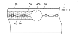
- FIGS. 8A to 8C are views for explaining a method of forming a sealing member in the light emitting device according to the first embodiment of the present invention
- FIG. 8A is a plan view thereof
- FIG. 8B is a plan view thereof
- Fig. 8C is a side view
- Fig. 8C is a cross-sectional view thereof.
- the sealing member 30 can be formed by coating using a dispenser, and as shown in FIGS. 8A to 8C, the discharge nozzle 600 of the dispenser is disposed opposite to a predetermined position on the substrate 10 The discharge nozzle 600 is driven along the longitudinal direction of the substrate 10 while discharging the sealing member material (phosphor-containing resin). At this time, the sealing member material is discharged so as to cover the wiring 40 and the wire 70 together with the LED 20.
- the sealing member material phosphor-containing resin
- the sealing member material is applied from one short side edge of the substrate 10 to the other short side edge in a single coating operation. As described above, by applying the sealing member material by one application operation, it is possible to suppress the occurrence of a chromaticity difference or the like in the module.
- the sealing member material After applying the sealing member material, the sealing member material is cured by a predetermined method. Thereby, the sealing member 30 of a predetermined shape can be formed.
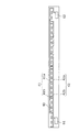
- FIG. 9A is a plan view of a light emitting device according to a second embodiment of the present invention.
- 9B is a cross-sectional view (a cross section in the longitudinal direction of the substrate) of the light emitting device according to the second embodiment of the present invention cut along the line XX ′ of FIG. 2C is a cross-sectional view (a cross-sectional view in the short direction of the substrate) of the light-emitting device according to the second embodiment of the present invention cut along the YY ′ line in (a).
- the light emitting device 200 according to the second embodiment of the present invention has the same basic configuration as the light emitting device 100 according to the first embodiment of the present invention.
- the light emitting device 200 according to the present embodiment differs from the light emitting device 100 according to the first embodiment in the arrangement position of the wiring pattern and the protection element, and the other configuration is basically the same. is there. Therefore, in FIG. 9, the same components as those shown in FIG. 2 are denoted by the same reference numerals, and the detailed description thereof is omitted.
- the light emitting device 200 according to the second embodiment of the present invention is more effective than the light emitting device 100 according to the first embodiment of the present invention.
- the first wiring 41 and the second wiring 42 are provided.
- the first wiring 41 and the second wiring 42 are electrically connected to the plurality of LEDs 20 and the protection elements 50 in the same manner as the wiring 40, and are pattern-formed in a predetermined shape on the substrate 10.
- the wiring 40 is a wiring for LED series connection, and is pattern-formed so as to connect a plurality of LEDs 20 (three LEDs 20 in the present embodiment) in series as in the first embodiment.
- the first wiring 41 and the second wiring 42 are wiring for LED parallel connection, and are pattern-formed so as to connect in parallel the LEDs 20 connected in series by the wiring 40. Further, the first wiring 41 and the second wiring 42 are also pattern-formed so as to connect the LED 20 and the protection element 50 in parallel.
- FIG. 10 is a circuit diagram of a light emitting device according to a second embodiment of the present invention.
- the circuit configuration of the LED 20 and the protection element 50 in the light emitting device 200 according to the second embodiment of the present invention is as shown in FIG. 10, and three LEDs 20 connected in series are connected in parallel and connected in series. The three LEDs 20 and the protection element 50 are connected in parallel.
- FIG. 11 is a view showing a wiring pattern in the light emitting device according to the second embodiment of the present invention.
- the first wiring 41 and the second wiring 42 respectively have linear portions 41 a and 42 b which are main wirings extending along the longitudinal direction of the substrate 10.
- the first wiring 41 has an extending portion 41 b extending in the lateral direction of the substrate 10 and from the linear portion 41 a to the linear portion 42 a of the second wiring 42.
- the second wiring 42 has an extending portion 42 b extending in the lateral direction of the substrate 10 and from the linear portion 42 a to the linear portion 41 a of the first wiring 41.
- the straight portion 41 a of the first wire 41 and the straight portion 42 a of the second wire 42 are formed substantially in parallel along the longitudinal direction of the substrate 10.
- a wire 40 patterned in a predetermined shape along the longitudinal direction of the substrate 10 is formed between the straight portion 41 a of the first wire 41 and the straight portion 42 a of the second wire 42.
- the extension portion 41 b of the first wiring 41 and the extension portion 42 b of the second wiring 42 are pattern-formed in order to connect the three LEDs 20 in series with the wiring 40 and also function as a bonding pad.
- the area other than the first electrode 61, the second electrode 62, and the wire bonding area on the substrate 10 is glass-coated. Therefore, at least the linear portion 41 a of the first wiring 41 and the linear portion 42 a of the second wiring 42 are coated with glass. In the present embodiment, a glass coat film having a thickness of about 40 ⁇ m is coated.
- the sealing member 30 is formed between the linear portion 41 a of the first wiring 41 and the linear portion 42 a of the second wiring 42.
- the distance (distance) between the straight portion 41 a of the first wiring 41 and the straight portion 42 a of the second wiring 42 is formed to be substantially the same as the line width of the sealing member 30. Is formed along the straight portion 41 a of the first wiring 41 and the straight portion 42 a of the second wiring 42.
- the first wiring 41 and the second wiring 42 are pattern-formed on the substrate 10 such that the line width of the sealing member 30 becomes a predetermined width.
- the LED 20 is disposed between the wires 40, between the wire 40 and the extension 41b, and between the wire 40 and the extension 42b.
- the LED 20 and the wire 40, the extension portion 41b or the extension portion 42b are bonded by a wire 70.
- the protection element 50 is disposed between the linear portion 41 a of the first wiring 41 and the linear portion 42 a of the second wiring 42, and the extension portion 41 b formed in the central portion of the substrate 10. It is arrange
- the protection element 50 and the extension portion 41 b or the extension portion 42 b are bonded by a wire 70.
- the protection elements 50 are arranged in a straight line with the LEDs 20. That is, the protection element 50 and all the LEDs 20 are arranged in one line. And all the wires bonded to the protection element 50 and the LED 20 are provided in the same direction as the linear direction of the sealing member 30.
- the protection elements 50 are arranged in a straight line together with the LEDs 20, and the protection elements 50 are also collectively sealed by the sealing member 30 together with the LEDs 20.
- all the wires bonded to the protection element 50 and the LED 20 are provided in the same direction as the linear direction of the sealing member 30.
- the shape can be stabilized to form the sealing member 30, and the sealing member 30 having a uniform line width can be easily formed.
- the change in the wettability of the sealing member 30 made of resin can be made constant intervals in the linear direction of the sealing member 30, so that the shape such as the thickness of the sealing member 30 can be made uniform in the linear direction.
- the sealing member material can be applied. This makes it possible to suppress the occurrence of color unevenness even in the case of a long elongated linear light source.
- FIGS. 12A to 12C are views for explaining a method of forming a sealing member in a light emitting device according to a second embodiment of the present invention
- FIG. 12A is a plan view thereof
- FIG. 12B is a plan view thereof
- FIG. 12C is a side view
- FIG. 12C is a cross-sectional view thereof.
- the sealing member 30 can be applied and formed using a dispenser. That is, as shown in FIGS. 12A to 12C, the discharge nozzle 600 of the dispenser is disposed opposite to the predetermined position on the substrate 10, and the discharge is performed while discharging the sealing member material (phosphor-containing resin) from the discharge nozzle 600. The nozzle 600 is driven along the longitudinal direction of the substrate 10. In the present embodiment, the sealing member material is applied from one short side edge of the substrate 10 to the other short side edge in a single coating operation.
- the sealing member material is applied to the region between the straight portion 41 a of the first wiring 41 and the straight portion 42 a of the second wiring 42.
- the expansion of the sealing member material in the short direction of the substrate 10 is restricted by the linear portion 41a of the first wiring 41 and the linear portion 42a of the second wiring 42, and the sealing member material is linear It can suppress flowing out beyond the part 42a.
- the uniformity is uniform.
- the sealing member 30 having a wide line width can be easily formed. Thereby, the chromaticity difference in the light emitting device can be suppressed.
- the sealing member 30 having a narrow line width can be easily formed. Therefore, even when the pitch of the LEDs 20 is large, the crushing feeling can be further suppressed.
- the sealing member material in the short direction of the substrate 10 can be regulated by the straight portion 41a and the straight portion 42a, the sealing member material has low thixotropy and high fluidity.
- the sealing member 30 having a narrow line width can be easily formed. Thus, the range of choices for the sealing member material is expanded.
- the surface of the sealing member 30 has a desired curved surface.
- the sealing member 30 in the latitudinal cross section can be configured to have a curve.
- the curve of the sealing member 30 in the latitudinal direction cross section can be configured to be a circular arc.
- the linear portion 41a and the linear portion 42a can be thickened. Thereby, the sealing member material can be further suppressed from flowing out beyond the straight portion 41a and the straight portion 42a.
- the linear portion 41a and the linear portion 42a may be plated to form a plating film to increase the thickness.
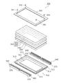
- FIG. 13 is an exploded perspective view of a backlight unit according to a third embodiment of the present invention.
- the backlight unit 300 is an edge light type backlight unit in which a light source is disposed on the side of a light guide plate, and includes a housing 310 and a reflective sheet.
- a light guide plate 330, a light emitting device 340, an optical sheet group 350, and a front frame 360 are provided.
- the housing 310 is a flat box type, and is formed by pressing a steel plate made of stainless steel or the like.
- the housing 310 has an opening 311 at the bottom, and a flange portion 312 is formed at the periphery of the opening of the housing 310.
- a screw hole 313 for fastening the front frame 360 is formed in the flange portion 312.
- the reflective sheet 320 is a sheet made of, for example, polyethylene terephthalate (PET), and causes the white light to travel into the light guide plate 330 while reflecting the white light from the light emitting device 340.
- PET polyethylene terephthalate
- the light guide plate 330 is a sheet made of, for example, polycarbonate (PC) or acrylic, and diffuses the light incident on the light guide plate 330 on the main surface (rear surface) on the reflective sheet 320 side facing the light emission surface (front surface) thereof.
- a dot pattern is printed, which is a lighting element for emitting light from the light emission surface.
- a light scattering element such as a light scattering structure formed on the rear surface of the light guide plate 330 by printing, molding or the like, a prism shape, or a light scattering element formed inside the light guide plate 330 is used.
- the optical sheet group 350 includes the diffusion sheet 351 having the same size and the same planar shape (rectangular shape), the prism sheet 352, and the polarizing sheet 353.
- the diffusion sheet 351 is, for example, a film made of PET and a film made of PC.
- the prism sheet 352 is a sheet made of, for example, polyester, and a regular prism pattern is formed of acrylic resin on one side.
- the front frame 360 is fixed to the flange portion 312 of the housing 310 by screwing the screw 361 into the screw hole 313 of the housing 310.
- the front frame 360 sandwiches the light guide plate 330 and the optical sheet group 350 together with the housing 310.
- the light emitting device 340 is a light emitting device according to the first and second embodiments of the present invention described above. In the present embodiment, four light emitting devices are used and provided on the heat sink 370 respectively. The four light emitting devices are disposed with the substrates of the light emitting device in contact with each other, as shown in FIG. The light emitting device 340 provided on the heat sink 370 is disposed such that the light emitting surface faces the side surface of the light guide plate 330.
- the heat sink 370 holds the light emitting device 340, and is made of, for example, a drawn material (angle member) made of L-shaped aluminum.
- the heat sink 370 is fixed to the housing 310 with a screw or the like.
- the backlight unit 300 according to the third embodiment of the present invention uses the light emitting device according to the first and second embodiments of the present invention, the luminance uniformity is suppressed with high luminance uniformity suppressed.
- a backlight unit can be realized.
- FIG. 14 is a cross-sectional view of a liquid crystal display device according to a fourth embodiment of the present invention.
- the liquid crystal display device 400 is, for example, a liquid crystal television or a liquid crystal monitor, and a liquid crystal display panel 410 and a back disposed on the back of the liquid crystal display panel 410.
- a light unit 420 and a housing 430 in which the liquid crystal display panel 410 and the backlight unit 420 are housed are provided.
- the backlight unit 420 the backlight unit according to the above-described fourth embodiment of the present invention is used.
- the backlight unit 420 is provided with a light emitting device 421 which is a linear light source.
- the light emitting device 421 the light emitting devices 100 and 200 according to the first and second embodiments of the present invention can be used.
- the liquid crystal display device 400 according to the fourth embodiment of the present invention uses the backlight unit 420 in which the chromaticity variation and the luminance variation are suppressed, a liquid crystal excellent in the display performance with high contrast and high luminance.
- a display device can be realized.
- FIG. 15 is a partially cutaway perspective view of a lighting device according to a fifth embodiment of the present invention.
- a lighting device 500 according to a fifth embodiment of the present invention is an LED lamp provided with the light emitting device according to the first and second embodiments of the present invention, and as shown in FIG. It corresponds to the fluorescent light of.
- a lighting device 500 includes a straight tube 510 configured of a long glass tube, a light emitting device 520 disposed in the straight tube 510, and a pair of base pins 530.
- the LED chip of the light emitting device 520 is supplied with power through the base 540, an adhesive (not shown) for joining (fixing) the light emitting device 520 in contact with the straight tube 510, and an LED chip of the light emitting device 520.
- a lighting circuit (not shown) for emitting light is provided.
- the lighting circuit may be provided in a lighting device outside the LED lamp.
- the light emitting device 520 the light emitting devices 100 and 200 according to the first and second embodiments of the present invention can be used. Further, in the present embodiment, a plurality of light emitting devices 520 are used, and as shown in FIG. 6, the substrates of the light emitting devices are disposed in contact with each other.
- the lighting apparatus 500 according to the fifth embodiment of the present invention uses the light emitting apparatus according to the first and second embodiments of the present invention, a lighting apparatus without luminance variation can be realized. .
- FIG. 16 is a schematic perspective view of a lighting device according to a sixth embodiment of the present invention.
- the present embodiment is an example in which the light emitting device 100 according to the first embodiment is applied as an illumination light source of a lighting device.
- the light emitting device 200 according to the second embodiment can also be applied to the present embodiment.
- the lighting device 1 is a base light, and includes a light emitting device 100, a lighting fixture 2, and a mounting member 3 for mounting the lighting fixture 2 and the light emitting device 100. Prepare. The light emitting device 100 is directly attached to the luminaire 2 together with the attachment member 3.
- the lighting apparatus 2 incorporates a lighting circuit and the like for controlling lighting of the light emitting device 100.
- the lighting fixture 2 has a screw hole provided so as to correspond to the through hole of the mounting member 3. That is, the position of the through hole of the mounting member 3 and the position of the screw hole of the lighting fixture 2 coincide with each other.
- the lighting fixture 2 can be formed, for example, by pressing an aluminum steel plate, and is directly attached, for example, to a ceiling or the like.
- the mounting member 3 is a long substrate, and for example, a metal base substrate made of a long aluminum substrate or the like can be used.
- the mounting member 3 is provided with a plurality of through holes, and when fixing the mounting member 3 and the luminaire 2, the through hole of the mounting member 3 and the screw hole of the luminaire 2 are made to coincide with each other.
- the screw 4 is screwed into the through hole and the screw hole through the screw 4.
- the through holes are alternately provided on opposite long sides of the mounting member 3.
- four through holes can be provided on one side of the long side of the mounting member 3 and three through holes can be provided on the other side of the long side so as not to face them.
- the fixing method of the mounting member 3 and the light emitting device 100 is not particularly limited, but the mounting member 3 and the light emitting device 100 are fixed by, for example, an adhesive or the like.
- a transparent cover may be provided to cover the light emitting device 100.
- a plurality of light emitting devices 100 may be provided in one lighting device.
- a plurality of light emitting devices 100 may be fixed to one mounting member 3, or a plurality of one mounting member 3 to which one light emitting device 100 is fixed may be mounted to the lighting fixture 2.
- the through holes of the attachment member 3 are provided on both sides of the long side of the substrate, but the through holes may be provided on only one long side (only one side).
- the screw hole is formed by providing the through hole in the mounting member 3, the structure in which the screw 4 is passed may be a notch instead of the through hole.
- a semicircular notch can be provided on the long side of the mounting member 3 and screwing can be performed using this notch.
- you may use what was standardized.
- the light emitting device 100 fixed to the mounting member 3 is attached to the lighting fixture 2 as a module, but the mounting member 3 itself may be used as the substrate 10 of the light emitting device 100. That is, the substrate 10 of the light emitting device 100 may be configured to also function as the mounting member 3, and the light emitting device 100 may be directly attached to the lighting fixture 2 without using the mounting member 3. In this case, in order to screw and fix, a through hole or a notch for attachment may be provided on the substrate 10 of the light emitting device 100.
- the light emitting device, the backlight unit, the liquid crystal display device, and the lighting device according to the present invention have been described above based on the respective embodiments, but the present invention is not limited to these embodiments.
- various modifications that can occur to those skilled in the art without departing from the scope of the present invention are also included in the scope of the present invention.
- the components in the plurality of embodiments may be arbitrarily combined without departing from the spirit of the invention.
- the said embodiment demonstrated the example of application to a backlight unit, a liquid crystal display device, or an illuminating device as an example of application of a light-emitting device, this is not restricted. Besides, it can be applied to, for example, a lamp light source of a copying machine, a guide light or a signboard device. Furthermore, it can also be used as a light source for industrial applications such as inspection line light sources.
- each light-emitting device was comprised so that white light might be emitted with blue LED and yellow fluorescent substance, it does not restrict to this.
- a phosphor-containing resin containing a red phosphor and a green phosphor may be used to emit white light by combining this with a blue LED.
- the semiconductor light emitting element used for each light emitting device is an LED, but a light emitting element such as a semiconductor laser, an organic EL (Electro Luminescence), or an inorganic EL may be used.
- a light emitting element such as a semiconductor laser, an organic EL (Electro Luminescence), or an inorganic EL may be used.
- the present invention relates to a light emitting device using a semiconductor light emitting element such as an LED as a light source, a backlight unit, a liquid crystal display device, an illuminating device such as a straight tube fluorescent lamp, an induction lamp, a signboard device, an electronic device such as a copier It can be widely used in industrial applications such as inspection line light sources.
- a semiconductor light emitting element such as an LED as a light source, a backlight unit, a liquid crystal display device, an illuminating device such as a straight tube fluorescent lamp, an induction lamp, a signboard device, an electronic device such as a copier It can be widely used in industrial applications such as inspection line light sources.
Landscapes
- Physics & Mathematics (AREA)
- Nonlinear Science (AREA)
- Optics & Photonics (AREA)
- Crystallography & Structural Chemistry (AREA)
- Chemical & Material Sciences (AREA)
- General Physics & Mathematics (AREA)
- Mathematical Physics (AREA)
- Led Device Packages (AREA)
- Non-Portable Lighting Devices Or Systems Thereof (AREA)
- Planar Illumination Modules (AREA)
- Fastening Of Light Sources Or Lamp Holders (AREA)
- Liquid Crystal (AREA)
- Arrangement Of Elements, Cooling, Sealing, Or The Like Of Lighting Devices (AREA)
Abstract
Description
まず、本発明の第1の実施形態に係る発光装置100の概略構成について、図1を用いて説明する。図1は、本発明の第1の実施形態に係る発光装置の概観斜視図である。
次に、本発明の第2の実施形態に係る発光装置200について、図9を用いて説明する。図9の(a)は、本発明の第2の実施形態に係る発光装置の平面図である。また、図9の(b)は、(a)のX-X’線に沿って切断した本発明の第2の実施形態に係る発光装置の断面図(基板長手方向断面)であり、図9の(c)は、(a)のY-Y’線に沿って切断した本発明の第2の実施形態に係る発光装置の断面図(基板短手方向断面)である。
以下、本発明の第1及び第2の実施形態に係る発光装置の適用例について、第3~第5の実施形態に基づいて説明する。
次に、本発明の第1及び第2の実施形態に係る発光装置を、液晶表示装置に適用した例について、図14を用いて説明する。図14は、本発明の第4の実施形態に係る液晶表示装置の断面図である。
次に、本発明の第1及び第2の実施形態に係る発光装置を、照明装置に適用した例について、図15を用いて説明する。図15は、本発明の第5の実施形態に係る照明装置の一部切り欠き斜視図である。
次に、本発明の第6の実施形態について、図16を用いて説明する。図16は、本発明の第6の実施形態に係る照明装置の概観斜視図である。本実施形態は、上記第1の実施形態に係る発光装置100を照明装置の照明用光源として適用した例である。なお、本実施形態には、第2の実施形態に係る発光装置200を適用することもできる。
2 照明器具
3 取り付け部材
4 ねじ
10、10A、10B、1010 基板
20、1020 LED
30、30A、30B、1030 封止部材
40 配線
41 第1配線
41a、42a 直線部
41b、42b 延出部
42 第2配線
50 保護素子
61、61A、61B 第1電極
62、62A、62B 第2電極
70 ワイヤ
100、200、100A、100B、340、421、520、1000 発光装置
110 発光部
300、420 バックライトユニット
310 筐体
311 開口
312 フランジ部
313 ネジ孔
320 反射シート
330 導光板
350 光学シート群
351 拡散シート
352 プリズムシート
353 偏光シート
360 前面枠
361 ネジ
370 ヒートシンク
400 液晶表示装置
410 液晶表示パネル
430 ハウジング
500 照明装置
510 直管
530 口金ピン
540 口金
600 吐出ノズル
1100 SMD型LED素子
1101 キャビティ
Claims (23)
- 長尺状の基板と、
前記基板上に当該基板の長手方向に沿って一直線状に配列された複数の半導体発光素子と、
光波長変換体を含み、前記複数の半導体発光素子を封止する封止部材と、を備え、
前記封止部材は、前記複数の半導体発光素子を一括封止するとともに、前記複数の半導体発光素子の配列方向に沿って直線状に形成されている
発光装置。 - 前記封止部材の直線方向の長さをLsとし、前記封止部材の線幅をWsとしたときに、
10≦Ls/Ws、である
請求項1に記載の発光装置。 - 前記半導体発光素子の前記直線方向の長さをLcとし、前記半導体発光素子の前記直線方向に直交する方向の長さをWcとすると、
Wc≦Lc、である
請求項2に記載の発光装置。 - Wc≦Ws/4、である
請求項3に記載の発光装置。 - 前記封止部材の高さをHsとし、前記封止部材の断面における前記封止部材中心から45度方向の長さをHs45とすると、
0.9≦Hs45/Hs≦1.1、である
請求項3又は請求項4に記載の発光装置。 - 0.4≦Hs/Ws≦0.6、である
請求項5に記載の発光装置。 - さらに、前記基板上に形成され、前記複数の半導体発光素子に電力を供給するための2つの電極を備え、
前記2つの電極のうちの一方の電極は、前記基板の長手方向の一方の端部に形成され、前記2つの電極のうちの他方の電極は、前記基板の長手方向の他方の端部に形成されており、
前記一方の電極と前記他方の電極は、前記封止部材を基準として前記基板の一方の長辺側に片寄せて形成される
請求項1~6のいずれか1項に記載の発光装置。 - 前記封止部材は、前記封止部材の線幅の中心を通る直線と前記基板の短手方向の中心を通る直線とが異なるように形成されている
請求項7に記載の発光装置。 - 前記封止部材は、前記基板の長手方向の両端縁まで形成されている
請求項1~8のいずれか1項に記載の発光装置。 - 前記複数の半導体発光素子は、同一のピッチで配列されており、
前記複数の半導体発光素子のうち両端に位置する2つの半導体発光素子のそれぞれは、当該両端に位置する半導体発光素子と前記基板の端縁との距離が前記ピッチの半分となるように配置される
請求項9に記載の発光装置。 - 前記封止部材の端部の輪郭線は曲率を有する
請求項9又は請求項10に記載の発光装置。 - さらに、前記複数の半導体発光素子のそれぞれにはワイヤがボンディングされており、
前記ワイヤそれぞれの少なくとも一部は、前記封止部材によって封止されており、
前記封止部材に封止される前記ワイヤの全てが、前記封止部材の直線方向と同じ方向で設けられている
請求項1~11のいずれか1項に記載の発光装置。 - さらに、前記複数の半導体発光素子を静電保護するための保護素子を備え、
前記保護素子は、前記複数の半導体発光素子とともに一直線状に配列されている
請求項1~11のいずれか1項に記載の発光装置。 - 前記保護素子及び前記複数の半導体発光素子の全ての素子は、同一のピッチで配列されている
請求項13に記載の発光装置。 - さらに、前記保護素子及び前記複数の半導体発光素子のそれぞれにはワイヤがボンディングされており、
前記ワイヤそれぞれの少なくとも一部は、前記封止部材によって封止されており、
前記封止部材に封止される前記ワイヤの全てが、前記封止部材の直線方向と同じ方向で設けられている
請求項13又は請求項14に記載の発光装置。 - さらに、前記複数の半導体発光素子と電気的に接続された第1配線及び第2配線を備え、
前記第1配線及び前記第2配線のそれぞれは、前記基板上において前記基板の長手方向に沿って略平行に形成された直線状の直線部を有し、
前記封止部材は、前記第1配線の直線部と前記第2配線の直線部との間に形成される
請求項1~15のいずれか1項に記載の発光装置。 - 前記第1配線の直線部及び前記第2配線の直線部は、ガラスコーティングされている
請求項16に記載の発光装置。 - 前記光波長変換体は、前記複数の半導体発光素子が発する光を励起する蛍光体である
請求項1~17のいずれか1項に記載の発光装置。 - 請求項1~18のいずれか1項に記載の発光装置を備える
バックライトユニット。 - 前記発光装置を複数備え、
複数の前記発光装置は、当該発光装置の基板同士を接触させて配置される
請求項19に記載のバックライトユニット。 - 請求項19又は請求項20に記載のバックライトユニットと、
前記バックライトユニットから照射される光の光路上に配置された液晶パネルと、を備える
液晶表示装置。 - 請求項1~18のいずれか1項に記載の発光装置を備える
照明装置。 - 前記発光装置を複数備え、
複数の前記発光装置は、当該発光装置の基板同士を接触させて配置される
請求項22に記載の照明装置。
Priority Applications (6)
| Application Number | Priority Date | Filing Date | Title |
|---|---|---|---|
| EP12774596.6A EP2701215B1 (en) | 2011-04-20 | 2012-03-12 | Light-emitting apparatus, backlight unit, liquid crystal display apparatus, and illumination apparatus |
| US14/112,079 US9299743B2 (en) | 2011-04-20 | 2012-03-12 | Light-emitting apparatus, backlight unit, liquid crystal display apparatus, and illumination apparatus |
| JP2012519648A JPWO2012144126A1 (ja) | 2011-04-20 | 2012-03-12 | 光源、バックライトユニット、液晶表示装置及び照明装置 |
| US15/651,187 USRE47780E1 (en) | 2011-04-20 | 2012-03-12 | Light-emitting apparatus, backlight unit, liquid crystal display apparatus, and illumination apparatus |
| CN201280018773.1A CN103493227B (zh) | 2011-04-20 | 2012-03-12 | 发光装置、背光单元、液晶显示装置以及照明装置 |
| US15/046,749 US9601669B2 (en) | 2011-04-20 | 2016-02-18 | Light-emitting apparatus, backlight unit, liquid crystal display apparatus, and illumination apparatus |
Applications Claiming Priority (2)
| Application Number | Priority Date | Filing Date | Title |
|---|---|---|---|
| JP2011094521 | 2011-04-20 | ||
| JP2011-094521 | 2011-04-20 |
Related Child Applications (2)
| Application Number | Title | Priority Date | Filing Date |
|---|---|---|---|
| US14/112,079 A-371-Of-International US9299743B2 (en) | 2011-04-20 | 2012-03-12 | Light-emitting apparatus, backlight unit, liquid crystal display apparatus, and illumination apparatus |
| US15/046,749 Continuation US9601669B2 (en) | 2011-04-20 | 2016-02-18 | Light-emitting apparatus, backlight unit, liquid crystal display apparatus, and illumination apparatus |
Publications (1)
| Publication Number | Publication Date |
|---|---|
| WO2012144126A1 true WO2012144126A1 (ja) | 2012-10-26 |
Family
ID=47041263
Family Applications (1)
| Application Number | Title | Priority Date | Filing Date |
|---|---|---|---|
| PCT/JP2012/001698 Ceased WO2012144126A1 (ja) | 2011-04-20 | 2012-03-12 | 発光装置、バックライトユニット、液晶表示装置及び照明装置 |
Country Status (6)
| Country | Link |
|---|---|
| US (3) | US9299743B2 (ja) |
| EP (1) | EP2701215B1 (ja) |
| JP (6) | JPWO2012144126A1 (ja) |
| CN (3) | CN105304800B (ja) |
| TW (1) | TWI554811B (ja) |
| WO (1) | WO2012144126A1 (ja) |
Cited By (13)
| Publication number | Priority date | Publication date | Assignee | Title |
|---|---|---|---|---|
| JP2014103355A (ja) * | 2012-11-22 | 2014-06-05 | Iwasaki Electric Co Ltd | 発光素子モジュール及び発光素子ユニット |
| JP2014112490A (ja) * | 2012-12-05 | 2014-06-19 | Panasonic Corp | 照明器具 |
| JP2014137931A (ja) * | 2013-01-17 | 2014-07-28 | Panasonic Corp | 光源装置及びそれを用いた照明器具 |
| JP2015038971A (ja) * | 2013-07-16 | 2015-02-26 | パナソニックIpマネジメント株式会社 | 基板、発光装置、照明用光源、および照明装置 |
| US20150062484A1 (en) * | 2013-08-30 | 2015-03-05 | Lg Display Co., Ltd. | Light emitting diode assembly and liquid crystal display device including the same |
| JP2015185216A (ja) * | 2014-03-20 | 2015-10-22 | 三菱電機株式会社 | 照明器具 |
| JP2017175024A (ja) * | 2016-03-24 | 2017-09-28 | パナソニックIpマネジメント株式会社 | 発光モジュール及び照明装置 |
| JP2018067573A (ja) * | 2016-10-17 | 2018-04-26 | パナソニックIpマネジメント株式会社 | 発光モジュール及び照明器具 |
| JP2018073950A (ja) * | 2016-10-27 | 2018-05-10 | パナソニックIpマネジメント株式会社 | 発光モジュール及び照明器具 |
| JP2019091944A (ja) * | 2013-09-11 | 2019-06-13 | 晶元光電股▲ふん▼有限公司Epistar Corporation | 可撓性発光ダイオードモジュール及び発光ダイオード電球 |
| JP2019114610A (ja) * | 2017-12-21 | 2019-07-11 | 東芝ライテック株式会社 | 光照射装置 |
| JP2019537229A (ja) * | 2016-09-30 | 2019-12-19 | 深▲せん▼市玲涛光電科技有限公司Shenzhen Lt Optoelectronics Co.,Ltd. | 帯状光源およびその製造方法、電子装置 |
| JP2022019555A (ja) * | 2020-07-17 | 2022-01-27 | エクセレンス オプトエレクトロニクス インコーポレイテッド | 面光源型ledデバイス |
Families Citing this family (30)
| Publication number | Priority date | Publication date | Assignee | Title |
|---|---|---|---|---|
| US9095018B2 (en) | 2012-05-18 | 2015-07-28 | Joled Inc. | Display panel and display panel manufacturing method |
| JP2014135471A (ja) * | 2012-12-10 | 2014-07-24 | Nitto Denko Corp | 発光装置、発光装置集合体および電極付基板 |
| JP6116560B2 (ja) * | 2012-06-15 | 2017-04-19 | シャープ株式会社 | 発光装置 |
| KR101658396B1 (ko) * | 2013-03-21 | 2016-09-21 | 엘지디스플레이 주식회사 | 디스플레이 장치 |
| TWI611722B (zh) * | 2013-09-06 | 2018-01-11 | Leadtrend Technology Corporation | 發光二極體之控制電路 |
| JP6311364B2 (ja) | 2014-03-10 | 2018-04-18 | セイコーエプソン株式会社 | 印刷サーバー、印刷システム、印刷管理プログラムおよび印刷管理方法 |
| JP6443751B2 (ja) * | 2015-02-12 | 2018-12-26 | パナソニックIpマネジメント株式会社 | 照明装置、照明システム及び移動体 |
| US9467190B1 (en) * | 2015-04-23 | 2016-10-11 | Connor Sport Court International, Llc | Mobile electronic device covering |
| KR102373025B1 (ko) * | 2015-06-12 | 2022-03-10 | 엘지전자 주식회사 | 광원모듈 및 이를 포함하는 면광원 장치 |
| JP2017009725A (ja) * | 2015-06-19 | 2017-01-12 | ソニー株式会社 | 表示装置 |
| EP3318109B1 (en) * | 2015-07-02 | 2026-04-01 | Lumileds LLC | An led lighting device |
| CN105068313A (zh) * | 2015-08-06 | 2015-11-18 | 北京工业大学 | 一种蓝光ld背光模组及显示装置 |
| KR101683771B1 (ko) * | 2016-03-22 | 2016-12-21 | 지스마트 주식회사 | 발광 면적의 확장이 가능한 투명전광판 |
| KR102555407B1 (ko) * | 2016-06-30 | 2023-07-14 | 엘지디스플레이 주식회사 | 플렉서블 유기발광 다이오드 표시장치 |
| JP6408516B2 (ja) * | 2016-07-01 | 2018-10-17 | ミネベアミツミ株式会社 | 面状照明装置及び基板 |
| CN111720760A (zh) * | 2016-08-26 | 2020-09-29 | 美蓓亚三美株式会社 | 面状照明装置和基板 |
| JP6735835B2 (ja) * | 2016-08-30 | 2020-08-05 | 株式会社Fuji | スプライシング装置 |
| US11307434B2 (en) * | 2016-09-01 | 2022-04-19 | 3D Live, Inc. | Stereoscopic display apparatus employing light emitting diodes with polarizing film/lens materials |
| TWI606172B (zh) * | 2016-10-28 | 2017-11-21 | 林 招慶 | 電子鎖的背光顯示構造 |
| FR3058778B1 (fr) * | 2016-11-15 | 2020-07-31 | Areva Np | Dispositif d'eclairage sous eau pour l'inspection visuelle d'un equipement de reacteur nucleaire et procede associe |
| JP7399849B2 (ja) * | 2017-09-15 | 2023-12-18 | ルミレッズ ホールディング ベーフェー | フレキシブルなライトストリップ |
| CN109841165B (zh) * | 2017-11-29 | 2021-11-16 | 利亚德光电股份有限公司 | 小间距led显示模块及其制作方法 |
| KR102253007B1 (ko) * | 2019-07-19 | 2021-05-18 | (주)티디엘 | Led 필름 디스플레이, 및 이의 제조 방법 |
| CN110925635A (zh) * | 2019-11-29 | 2020-03-27 | 广东华辉煌光电科技有限公司 | 一种灯条封胶结构 |
| KR20210079898A (ko) * | 2019-12-20 | 2021-06-30 | 엘지디스플레이 주식회사 | 표시장치 |
| JP7502141B2 (ja) * | 2020-10-07 | 2024-06-18 | 伊東電機株式会社 | 発光素子モジュール、防爆照明器具、及び発光素子モジュールの製造方法 |
| FR3121308B1 (fr) | 2021-03-23 | 2023-12-22 | Appleton Grp Llc | Moteur de lumière à LED classé ZONE IEC 1 utilisant une optique pré-moulée |
| US11906133B2 (en) | 2022-03-31 | 2024-02-20 | Alliance Sports Group, L.P. | Outdoor lighting apparatus |
| FR3135511B1 (fr) | 2022-05-16 | 2024-07-19 | Appleton Grp Llc | Moteur de lumière à DEL certifié IEC ZONE utilisant une couche d’encapsulation pré-moulée et une feuille de métal |
| CN115158156B (zh) * | 2022-07-14 | 2024-08-30 | 重庆睿博光电股份有限公司 | 适用于立体线形氛围灯的立体效果厚壁光导 |
Citations (5)
| Publication number | Priority date | Publication date | Assignee | Title |
|---|---|---|---|---|
| JP2006013087A (ja) | 2004-06-25 | 2006-01-12 | Nichia Chem Ind Ltd | 半導体発光装置 |
| JP2007288200A (ja) * | 2006-04-18 | 2007-11-01 | Harvatek Corp | 発光ダイオードチップの封止構造および発光ダイオードチップ構造のパッケージ方法 |
| JP2009009898A (ja) * | 2007-06-29 | 2009-01-15 | Toshiba Lighting & Technology Corp | 照明装置および照明器具 |
| JP2010118531A (ja) * | 2008-11-13 | 2010-05-27 | Stanley Electric Co Ltd | 白色照明装置および車輛用灯具 |
| JP2011061056A (ja) * | 2009-09-11 | 2011-03-24 | Stanley Electric Co Ltd | 線状発光装置、その製造方法並びに面光源装置 |
Family Cites Families (63)
| Publication number | Priority date | Publication date | Assignee | Title |
|---|---|---|---|---|
| JPS5257731A (en) | 1975-11-06 | 1977-05-12 | Matsushita Electric Ind Co Ltd | Light source for information reading element |
| JPS52120552U (ja) * | 1976-03-02 | 1977-09-13 | ||
| JPH0545812U (ja) * | 1991-11-22 | 1993-06-18 | 株式会社小糸製作所 | 車輌用灯具 |
| JPH05299702A (ja) * | 1992-04-17 | 1993-11-12 | Stanley Electric Co Ltd | Ledアレイ |
| JP3027479B2 (ja) | 1992-10-08 | 2000-04-04 | ローム株式会社 | 発光ダイオード光源 |
| JPH06314858A (ja) | 1993-04-30 | 1994-11-08 | Toshiba Lighting & Technol Corp | 配線基板、発光ダイオードアレイ、照明装置および指針 |
| JP3616127B2 (ja) * | 1994-02-09 | 2005-02-02 | 松下電器産業株式会社 | 発光ダイオード整列光源 |
| US20040061220A1 (en) | 1996-03-22 | 2004-04-01 | Chuichi Miyazaki | Semiconductor device and manufacturing method thereof |
| CN1167249C (zh) | 1999-01-26 | 2004-09-15 | 罗姆股份有限公司 | 线状光源及备有此光源的图象读取装置 |
| JP2002299697A (ja) * | 2001-03-29 | 2002-10-11 | Mitsubishi Electric Lighting Corp | Led光源デバイス及び照明器具 |
| JP4356383B2 (ja) | 2003-07-03 | 2009-11-04 | パナソニック電工株式会社 | 発光装置の製造方法 |
| US20050285926A1 (en) * | 2004-06-29 | 2005-12-29 | Fuji Photo Film Co., Ltd. | Light source assembly, method of producing light source assembly, and color thermal printer |
| JP2006179544A (ja) | 2004-12-21 | 2006-07-06 | Matsushita Electric Ind Co Ltd | Led光源 |
| KR101017921B1 (ko) * | 2005-06-13 | 2011-03-08 | 가부시키가이샤후지쿠라 | 발광 소자 실장용 기판, 발광 모듈 및 조명 장치 |
| JP5214128B2 (ja) | 2005-11-22 | 2013-06-19 | シャープ株式会社 | 発光素子及び発光素子を備えたバックライトユニット |
| JP5555971B2 (ja) | 2006-07-18 | 2014-07-23 | 日亜化学工業株式会社 | 線状発光装置およびそれを用いた面状発光装置 |
| US8052303B2 (en) | 2006-09-12 | 2011-11-08 | Huizhou Light Engine Ltd. | Integrally formed single piece light emitting diode light wire and uses thereof |
| JP2009528685A (ja) | 2006-09-12 | 2009-08-06 | ポール・ロ | 一体的に成形された一体成形発光ダイオードライトワイヤ |
| US8807796B2 (en) | 2006-09-12 | 2014-08-19 | Huizhou Light Engine Ltd. | Integrally formed light emitting diode light wire and uses thereof |
| US8567992B2 (en) | 2006-09-12 | 2013-10-29 | Huizhou Light Engine Ltd. | Integrally formed light emitting diode light wire and uses thereof |
| JP2008071954A (ja) | 2006-09-14 | 2008-03-27 | Mimaki Denshi Buhin Kk | 光源装置 |
| JP2008078401A (ja) | 2006-09-21 | 2008-04-03 | Toshiba Lighting & Technology Corp | 照明装置 |
| US20080074884A1 (en) | 2006-09-25 | 2008-03-27 | Thye Linn Mok | Compact high-intensty LED-based light source and method for making the same |
| JP5060172B2 (ja) | 2007-05-29 | 2012-10-31 | 岩谷産業株式会社 | 半導体発光装置 |
| JP2009010308A (ja) | 2007-05-31 | 2009-01-15 | Toshiba Lighting & Technology Corp | 発光装置 |
| JP2009032746A (ja) | 2007-07-24 | 2009-02-12 | Harison Toshiba Lighting Corp | 発光装置及び発光ユニット |
| US20100195322A1 (en) | 2007-07-30 | 2010-08-05 | Sharp Kabushiki Kaisha | Light emitting device, illuminating apparatus and clean room equipped with illuminating apparatus |
| JP2009038202A (ja) | 2007-08-01 | 2009-02-19 | Fujikura Ltd | 発光素子実装用基板、発光素子モジュール、照明装置、表示装置及び交通信号機 |
| JP5097471B2 (ja) * | 2007-08-03 | 2012-12-12 | シャープ株式会社 | 発光装置の製造方法 |
| JP5128881B2 (ja) * | 2007-08-31 | 2013-01-23 | パナソニック株式会社 | 実装用基板及び発光モジュール |
| JP5401025B2 (ja) | 2007-09-25 | 2014-01-29 | 三洋電機株式会社 | 発光モジュールおよびその製造方法 |
| JP4893582B2 (ja) | 2007-10-25 | 2012-03-07 | 豊田合成株式会社 | 光源装置 |
| TWI352419B (en) * | 2007-11-30 | 2011-11-11 | Gigno Technology Co Ltd | Light emitting unit |
| US20090140271A1 (en) * | 2007-11-30 | 2009-06-04 | Wen-Jyh Sah | Light emitting unit |
| JP5169263B2 (ja) | 2008-02-01 | 2013-03-27 | 日亜化学工業株式会社 | 発光装置の製造方法及び発光装置 |
| US8049237B2 (en) | 2007-12-28 | 2011-11-01 | Nichia Corporation | Light emitting device |
| JP5119917B2 (ja) | 2007-12-28 | 2013-01-16 | 日亜化学工業株式会社 | 発光装置 |
| JP5216362B2 (ja) | 2008-02-20 | 2013-06-19 | スタンレー電気株式会社 | Led光源ユニット |
| TW200939869A (en) * | 2008-03-05 | 2009-09-16 | Harvatek Corp | An LED chip package structure with a high-efficiency heat-dissipating substrate and packaging method thereof |
| WO2009141982A1 (ja) | 2008-05-19 | 2009-11-26 | 株式会社 東芝 | 線状白色光源ならびにそれを用いたバックライトおよび液晶表示装置 |
| KR20100003321A (ko) * | 2008-06-24 | 2010-01-08 | 삼성전자주식회사 | 발광 소자, 이를 포함하는 발광 장치, 상기 발광 소자 및발광 장치의 제조 방법 |
| JP2010092670A (ja) | 2008-10-06 | 2010-04-22 | Panasonic Corp | 照明装置及び画像表示装置 |
| US8342720B2 (en) | 2008-10-10 | 2013-01-01 | Stanley Electric Co., Ltd. | Vehicle light and road illumination device |
| JP4801751B2 (ja) * | 2009-02-27 | 2011-10-26 | シャープ株式会社 | Ledモジュール及びled光源装置 |
| JP2010199513A (ja) | 2009-02-27 | 2010-09-09 | Panasonic Corp | 発光装置及びこの発光装置を備えた照明装置 |
| KR101670981B1 (ko) | 2009-03-31 | 2016-10-31 | 서울반도체 주식회사 | 튜브형 또는 채널형의 led 조명장치 |
| JP5275140B2 (ja) | 2009-06-04 | 2013-08-28 | 昭和電工株式会社 | 照明装置及び発光装置 |
| TWI381564B (zh) | 2009-08-06 | 2013-01-01 | 億光電子工業股份有限公司 | 發光二極體 |
| WO2011025173A2 (en) | 2009-08-27 | 2011-03-03 | Lg Electronics Inc. | Backlight unit and display device |
| JP5506313B2 (ja) | 2009-09-30 | 2014-05-28 | スタンレー電気株式会社 | 車両ヘッドライト用発光ダイオード光源 |
| TWI394299B (zh) | 2009-11-06 | 2013-04-21 | 旭明光電股份有限公司 | 具有外移式電極之垂直發光二極體 |
| CN201788969U (zh) * | 2009-12-30 | 2011-04-06 | 宏齐科技股份有限公司 | 一种具高导热及导光功能的发光模组及应用装置 |
| KR100973330B1 (ko) | 2010-01-22 | 2010-07-30 | 주식회사 비에스엘 | Led직관램프용 led패키지 모듈 및 그 제조방법 |
| JP4932064B2 (ja) | 2010-03-11 | 2012-05-16 | パナソニック株式会社 | 発光モジュール、光源装置、液晶表示装置および発光モジュールの製造方法 |
| US8820950B2 (en) | 2010-03-12 | 2014-09-02 | Toshiba Lighting & Technology Corporation | Light emitting device and illumination apparatus |
| JP3161182U (ja) | 2010-05-12 | 2010-07-22 | 雷徳光股▲分▼有限公司 | 発光ダイオードのパッケージ構造 |
| WO2012001938A1 (ja) | 2010-06-28 | 2012-01-05 | パナソニック株式会社 | 発光装置、バックライトユニット、液晶表示装置及び照明装置 |
| CN102315371A (zh) * | 2010-07-05 | 2012-01-11 | 松下电工株式会社 | 发光装置 |
| JP4926303B1 (ja) | 2010-12-27 | 2012-05-09 | パナソニック株式会社 | 発光装置およびランプ |
| JP3167034U (ja) | 2011-01-20 | 2011-03-31 | 睿騰光電科技股▲ふん▼有限公司 | 発光ダイオードモジュール構造 |
| CN103339751B (zh) | 2011-11-15 | 2016-12-14 | 松下知识产权经营株式会社 | 发光模块以及使用该发光模块的灯 |
| EP2658000B1 (en) * | 2012-03-13 | 2018-05-02 | Panasonic Intellectual Property Management Co., Ltd. | Substrate, light-emitting device, and illumination device |
| US20140321109A1 (en) * | 2013-04-27 | 2014-10-30 | GEM Weltronics TWN Corporation | Light emitting diode (led) light tube |
-
2012
- 2012-03-12 WO PCT/JP2012/001698 patent/WO2012144126A1/ja not_active Ceased
- 2012-03-12 CN CN201510808901.8A patent/CN105304800B/zh active Active
- 2012-03-12 CN CN201280018773.1A patent/CN103493227B/zh active Active
- 2012-03-12 CN CN201610213194.2A patent/CN105826311B/zh active Active
- 2012-03-12 EP EP12774596.6A patent/EP2701215B1/en active Active
- 2012-03-12 JP JP2012519648A patent/JPWO2012144126A1/ja active Pending
- 2012-03-12 TW TW101108215A patent/TWI554811B/zh active
- 2012-03-12 US US14/112,079 patent/US9299743B2/en not_active Ceased
- 2012-03-12 US US15/651,187 patent/USRE47780E1/en active Active
-
2013
- 2013-04-01 JP JP2013076098A patent/JP5884019B2/ja active Active
-
2014
- 2014-09-17 JP JP2014189426A patent/JP6004379B2/ja active Active
- 2014-09-17 JP JP2014189427A patent/JP2015029122A/ja active Pending
-
2015
- 2015-08-19 JP JP2015162297A patent/JP6436434B2/ja active Active
-
2016
- 2016-02-18 US US15/046,749 patent/US9601669B2/en active Active
-
2017
- 2017-10-27 JP JP2017208172A patent/JP6617760B2/ja active Active
Patent Citations (5)
| Publication number | Priority date | Publication date | Assignee | Title |
|---|---|---|---|---|
| JP2006013087A (ja) | 2004-06-25 | 2006-01-12 | Nichia Chem Ind Ltd | 半導体発光装置 |
| JP2007288200A (ja) * | 2006-04-18 | 2007-11-01 | Harvatek Corp | 発光ダイオードチップの封止構造および発光ダイオードチップ構造のパッケージ方法 |
| JP2009009898A (ja) * | 2007-06-29 | 2009-01-15 | Toshiba Lighting & Technology Corp | 照明装置および照明器具 |
| JP2010118531A (ja) * | 2008-11-13 | 2010-05-27 | Stanley Electric Co Ltd | 白色照明装置および車輛用灯具 |
| JP2011061056A (ja) * | 2009-09-11 | 2011-03-24 | Stanley Electric Co Ltd | 線状発光装置、その製造方法並びに面光源装置 |
Non-Patent Citations (1)
| Title |
|---|
| See also references of EP2701215A4 |
Cited By (20)
| Publication number | Priority date | Publication date | Assignee | Title |
|---|---|---|---|---|
| JP2014103355A (ja) * | 2012-11-22 | 2014-06-05 | Iwasaki Electric Co Ltd | 発光素子モジュール及び発光素子ユニット |
| JP2014112490A (ja) * | 2012-12-05 | 2014-06-19 | Panasonic Corp | 照明器具 |
| JP2014137931A (ja) * | 2013-01-17 | 2014-07-28 | Panasonic Corp | 光源装置及びそれを用いた照明器具 |
| JP2015038971A (ja) * | 2013-07-16 | 2015-02-26 | パナソニックIpマネジメント株式会社 | 基板、発光装置、照明用光源、および照明装置 |
| KR102067420B1 (ko) * | 2013-08-30 | 2020-01-17 | 엘지디스플레이 주식회사 | 발광다이오드어셈블리 및 그를 포함한 액정표시장치 |
| KR20150025728A (ko) * | 2013-08-30 | 2015-03-11 | 엘지디스플레이 주식회사 | 발광다이오드어셈블리 및 그를 포함한 액정표시장치 |
| CN104421771A (zh) * | 2013-08-30 | 2015-03-18 | 乐金显示有限公司 | 发光二极管组件以及包括该组件的液晶显示装置 |
| US9429701B2 (en) * | 2013-08-30 | 2016-08-30 | Lg Display Co., Ltd. | Light emitting diode assembly and liquid crystal display device including the same |
| US20150062484A1 (en) * | 2013-08-30 | 2015-03-05 | Lg Display Co., Ltd. | Light emitting diode assembly and liquid crystal display device including the same |
| USRE49031E1 (en) | 2013-09-11 | 2022-04-12 | Epistar Corporation | Flexible LED assemblies and LED light bulbs |
| JP2019091944A (ja) * | 2013-09-11 | 2019-06-13 | 晶元光電股▲ふん▼有限公司Epistar Corporation | 可撓性発光ダイオードモジュール及び発光ダイオード電球 |
| JP2015185216A (ja) * | 2014-03-20 | 2015-10-22 | 三菱電機株式会社 | 照明器具 |
| JP2017175024A (ja) * | 2016-03-24 | 2017-09-28 | パナソニックIpマネジメント株式会社 | 発光モジュール及び照明装置 |
| JP2019537229A (ja) * | 2016-09-30 | 2019-12-19 | 深▲せん▼市玲涛光電科技有限公司Shenzhen Lt Optoelectronics Co.,Ltd. | 帯状光源およびその製造方法、電子装置 |
| JP2018067573A (ja) * | 2016-10-17 | 2018-04-26 | パナソニックIpマネジメント株式会社 | 発光モジュール及び照明器具 |
| JP2018073950A (ja) * | 2016-10-27 | 2018-05-10 | パナソニックIpマネジメント株式会社 | 発光モジュール及び照明器具 |
| JP2019114610A (ja) * | 2017-12-21 | 2019-07-11 | 東芝ライテック株式会社 | 光照射装置 |
| JP7135316B2 (ja) | 2017-12-21 | 2022-09-13 | 東芝ライテック株式会社 | 光照射装置 |
| JP2022019555A (ja) * | 2020-07-17 | 2022-01-27 | エクセレンス オプトエレクトロニクス インコーポレイテッド | 面光源型ledデバイス |
| JP7341186B2 (ja) | 2020-07-17 | 2023-09-08 | エクセレンス オプトエレクトロニクス インコーポレイテッド | 面光源型ledデバイス |
Also Published As
| Publication number | Publication date |
|---|---|
| JP6004379B2 (ja) | 2016-10-05 |
| USRE47780E1 (en) | 2019-12-24 |
| JP5884019B2 (ja) | 2016-03-15 |
| US9601669B2 (en) | 2017-03-21 |
| JP2018046284A (ja) | 2018-03-22 |
| EP2701215A4 (en) | 2014-09-03 |
| JP2014241448A (ja) | 2014-12-25 |
| CN105826311A (zh) | 2016-08-03 |
| JPWO2012144126A1 (ja) | 2014-07-28 |
| CN105826311B (zh) | 2019-06-25 |
| JP6436434B2 (ja) | 2018-12-12 |
| JP2015216405A (ja) | 2015-12-03 |
| JP6617760B2 (ja) | 2019-12-11 |
| JP2015029122A (ja) | 2015-02-12 |
| JP2013141021A (ja) | 2013-07-18 |
| CN105304800B (zh) | 2019-06-11 |
| EP2701215A1 (en) | 2014-02-26 |
| CN105304800A (zh) | 2016-02-03 |
| CN103493227A (zh) | 2014-01-01 |
| CN103493227B (zh) | 2016-09-28 |
| EP2701215B1 (en) | 2018-01-03 |
| US20140036205A1 (en) | 2014-02-06 |
| US9299743B2 (en) | 2016-03-29 |
| TW201300908A (zh) | 2013-01-01 |
| US20160163933A1 (en) | 2016-06-09 |
| TWI554811B (zh) | 2016-10-21 |
Similar Documents
| Publication | Publication Date | Title |
|---|---|---|
| JP6617760B2 (ja) | 発光装置、液晶表示装置及び照明器具 | |
| US8450929B2 (en) | Light emitting device, backlight unit, liquid crystal display apparatus, and lighting apparatus | |
| US8847251B2 (en) | Substrate, light-emitting device, and lighting apparatus having a largest gap between two lines at light-emitting element mounting position | |
| CN1928425A (zh) | 利用柔性电路载体的薄型光源 | |
| JP6344689B2 (ja) | 基板、発光装置、照明用光源、および照明装置 | |
| EP2360417A2 (en) | Light-emitting device and illumination device | |
| CN103797593A (zh) | 发光装置及使用它的照明装置 | |
| JP2012195317A (ja) | ランプ及び照明装置 | |
| JP5568418B2 (ja) | 発光装置、バックライトユニット、液晶表示装置及び照明装置 | |
| JP2013191667A (ja) | 発光装置及び照明装置 | |
| JP2011077084A (ja) | Led照明装置および液晶表示装置 | |
| KR20130013955A (ko) | 발광소자 패키지 모듈 및 이를 포함하는 조명시스템 | |
| JP2020035637A (ja) | 発光装置及びそれを備えた照明装置 | |
| JP2020035787A (ja) | 発光装置 | |
| KR20120009001A (ko) | 발광 소자 |
Legal Events
| Date | Code | Title | Description |
|---|---|---|---|
| ENP | Entry into the national phase |
Ref document number: 2012519648 Country of ref document: JP Kind code of ref document: A |
|
| 121 | Ep: the epo has been informed by wipo that ep was designated in this application |
Ref document number: 12774596 Country of ref document: EP Kind code of ref document: A1 |
|
| WWE | Wipo information: entry into national phase |
Ref document number: 14112079 Country of ref document: US Ref document number: 2012774596 Country of ref document: EP |
|
| NENP | Non-entry into the national phase |
Ref country code: DE |