WO2012144339A1 - 情報取得装置および物体検出装置 - Google Patents
情報取得装置および物体検出装置 Download PDFInfo
- Publication number
- WO2012144339A1 WO2012144339A1 PCT/JP2012/059446 JP2012059446W WO2012144339A1 WO 2012144339 A1 WO2012144339 A1 WO 2012144339A1 JP 2012059446 W JP2012059446 W JP 2012059446W WO 2012144339 A1 WO2012144339 A1 WO 2012144339A1
- Authority
- WO
- WIPO (PCT)
- Prior art keywords
- dot pattern
- optical system
- segment
- area
- information acquisition
- Prior art date
- Legal status (The legal status is an assumption and is not a legal conclusion. Google has not performed a legal analysis and makes no representation as to the accuracy of the status listed.)
- Ceased
Links
Images







Classifications
-
- G—PHYSICS
- G01—MEASURING; TESTING
- G01S—RADIO DIRECTION-FINDING; RADIO NAVIGATION; DETERMINING DISTANCE OR VELOCITY BY USE OF RADIO WAVES; LOCATING OR PRESENCE-DETECTING BY USE OF THE REFLECTION OR RERADIATION OF RADIO WAVES; ANALOGOUS ARRANGEMENTS USING OTHER WAVES
- G01S17/00—Systems using the reflection or reradiation of electromagnetic waves other than radio waves, e.g. lidar systems
- G01S17/02—Systems using the reflection of electromagnetic waves other than radio waves
- G01S17/06—Systems determining position data of a target
- G01S17/46—Indirect determination of position data
- G01S17/48—Active triangulation systems, i.e. using the transmission and reflection of electromagnetic waves other than radio waves
-
- G—PHYSICS
- G01—MEASURING; TESTING
- G01B—MEASURING LENGTH, THICKNESS OR SIMILAR LINEAR DIMENSIONS; MEASURING ANGLES; MEASURING AREAS; MEASURING IRREGULARITIES OF SURFACES OR CONTOURS
- G01B11/00—Measuring arrangements characterised by the use of optical techniques
- G01B11/24—Measuring arrangements characterised by the use of optical techniques for measuring contours or curvatures
- G01B11/25—Measuring arrangements characterised by the use of optical techniques for measuring contours or curvatures by projecting a pattern, e.g. one or more lines, moiré fringes on the object
-
- G—PHYSICS
- G01—MEASURING; TESTING
- G01B—MEASURING LENGTH, THICKNESS OR SIMILAR LINEAR DIMENSIONS; MEASURING ANGLES; MEASURING AREAS; MEASURING IRREGULARITIES OF SURFACES OR CONTOURS
- G01B11/00—Measuring arrangements characterised by the use of optical techniques
- G01B11/24—Measuring arrangements characterised by the use of optical techniques for measuring contours or curvatures
- G01B11/25—Measuring arrangements characterised by the use of optical techniques for measuring contours or curvatures by projecting a pattern, e.g. one or more lines, moiré fringes on the object
- G01B11/2513—Measuring arrangements characterised by the use of optical techniques for measuring contours or curvatures by projecting a pattern, e.g. one or more lines, moiré fringes on the object with several lines being projected in more than one direction, e.g. grids, patterns
-
- G—PHYSICS
- G01—MEASURING; TESTING
- G01C—MEASURING DISTANCES, LEVELS OR BEARINGS; SURVEYING; NAVIGATION; GYROSCOPIC INSTRUMENTS; PHOTOGRAMMETRY OR VIDEOGRAMMETRY
- G01C3/00—Measuring distances in line of sight; Optical rangefinders
- G01C3/02—Details
- G01C3/06—Use of electric means to obtain final indication
- G01C3/08—Use of electric radiation detectors
Definitions
- the present invention relates to an object detection apparatus that detects an object in a target area based on a state of reflected light when light is projected onto the target area, and an information acquisition apparatus suitable for use in the object detection apparatus.
- An object detection apparatus using a so-called distance image sensor can detect not only a planar image on a two-dimensional plane but also the shape and movement of the detection target object in the depth direction.
- light in a predetermined wavelength band is projected from a laser light source or LED (Light Emitting Diode) onto a target area, and the reflected light is received (imaged) by a photodetector such as a CMOS image sensor.
- CMOS image sensor complementary metal-sector
- a distance image sensor of a type that irradiates a target area with laser light having a predetermined dot pattern reflected light from the target area of laser light having a dot pattern is received by a photodetector. Then, based on the light receiving position of the dot on the photodetector, the distance to each part of the detection target object (irradiation position of each dot on the detection target object) is detected using a triangulation method (for example, non- Patent Document 1).
- laser light having a dot pattern is generated by diffracting laser light emitted from a laser light source by a diffractive optical element.
- the diffractive optical element is designed, for example, so that the dot pattern on the target area is uniformly distributed with the same luminance.
- the brightness of the dots in the peripheral portion may be smaller than the brightness of the dots in the central portion in the target area due to a molding error or the like generated in the diffractive optical element.
- the present invention has been made to solve such a problem, and an object of the present invention is to provide an information acquisition device and an object detection device that can suppress a decrease in the accuracy of distance detection in the periphery of a dot pattern.
- the 1st aspect of this invention is related with the information acquisition apparatus which acquires the information of a target area
- the information acquisition apparatus is arranged so as to be aligned with a projection optical system that projects a laser beam with a predetermined dot pattern on the target area, a predetermined distance away from the projection optical system, and the target area And a distance acquisition unit that acquires the distance to each part of the object existing in the target area based on the dot pattern imaged by the light receiving optical system.
- the projection optical system is configured such that the dot density of the dot pattern in the target region is smaller in the peripheral portion than in the central portion of the dot pattern.
- the distance acquisition unit divides a reference dot pattern reflected by a reference surface and imaged by the light receiving optical system into segment areas, and captures the target area at the time of distance measurement and acquires the captured dot pattern and each segment area The distance for each segment area is obtained by collating with the dots.
- the segment area is set so that the peripheral area is larger than the central area of the reference dot pattern.
- the second aspect of the present invention relates to an object detection apparatus.
- the object detection apparatus according to this aspect includes the information acquisition apparatus according to the first aspect.
- an information acquisition device and an object detection device that can suppress a decrease in accuracy of distance detection in the peripheral portion of a dot pattern.
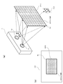
- FIG. 1 It is a figure which shows schematic structure of the object detection apparatus which concerns on embodiment. It is a figure which shows the structure of the information acquisition apparatus and information processing apparatus which concern on embodiment. It is the figure which shows typically the irradiation state of the laser beam with respect to the target area
- an information acquisition device of a type that irradiates a target area with laser light having a predetermined dot pattern is exemplified.
- FIG. 1 shows a schematic configuration of the object detection apparatus according to the present embodiment.
- the object detection device includes an information acquisition device 1 and an information processing device 2.
- the television 3 is controlled by a signal from the information processing device 2.
- a device including the information acquisition device 1 and the information processing device 2 corresponds to the object detection device of the present invention.
- the information acquisition device 1 projects infrared light over the entire target area and receives the reflected light with a CMOS image sensor, whereby the distance between each part of the object in the target area (hereinafter referred to as “three-dimensional distance information”). To get.
- the acquired three-dimensional distance information is sent to the information processing apparatus 2 via the cable 4.
- the information processing apparatus 2 is, for example, a controller for TV control, a game machine, a personal computer, or the like.
- the information processing device 2 detects an object in the target area based on the three-dimensional distance information received from the information acquisition device 1, and controls the television 3 based on the detection result.
- the information processing apparatus 2 detects a person based on the received three-dimensional distance information and detects the movement of the person from the change in the three-dimensional distance information.
- the information processing device 2 is a television control controller
- the information processing device 2 detects the person's gesture from the received three-dimensional distance information and outputs a control signal to the television 3 in accordance with the gesture.
- the application program to be installed is installed.
- the user can cause the television 3 to execute a predetermined function such as channel switching or volume up / down by making a predetermined gesture while watching the television 3.
- the information processing device 2 when the information processing device 2 is a game machine, the information processing device 2 detects the person's movement from the received three-dimensional distance information, and displays a character on the television screen according to the detected movement.
- An application program that operates and changes the game battle situation is installed. In this case, the user can experience a sense of realism in which he / she plays a game as a character on the television screen by making a predetermined movement while watching the television 3.
- FIG. 2 is a diagram showing the configuration of the information acquisition device 1 and the information processing device 2.
- the information acquisition apparatus 1 includes a projection optical system 11 and a light receiving optical system 12 as a configuration of the optical unit.
- the information acquisition device 1 includes a CPU (Central Processing Unit) 21, a laser driving circuit 22, an imaging signal processing circuit 23, an input / output circuit 24, and a memory 25 as a circuit unit.
- CPU Central Processing Unit
- the projection optical system 11 irradiates a target area with laser light having a predetermined dot pattern.
- the light receiving optical system 12 receives the laser beam reflected from the target area.
- the configurations of the projection optical system 11 and the light receiving optical system 12 will be described later with reference to FIGS.
- the CPU 21 controls each unit according to a control program stored in the memory 25.
- the CPU 21 has functions of a laser control unit 21 a for controlling a laser light source 111 (described later) in the projection optical system 11 and a three-dimensional distance calculation unit 21 b for generating three-dimensional distance information. Is granted.
- the laser drive circuit 22 drives a laser light source 111 (described later) according to a control signal from the CPU 21.
- the imaging signal processing circuit 23 controls a CMOS image sensor 123 (described later) in the light receiving optical system 12 and sequentially takes in each pixel signal (charge) generated by the CMOS image sensor 123 for each line. Then, the captured signals are sequentially output to the CPU 21.
- CPU21 calculates the distance from the information acquisition apparatus 1 to each part of a detection target based on the signal (imaging signal) supplied from the imaging signal processing circuit 23 by the process by the three-dimensional distance calculation part 21b.
- the input / output circuit 24 controls data communication with the information processing apparatus 2.
- the information processing apparatus 2 includes a CPU 31, an input / output circuit 32, and a memory 33.
- the information processing apparatus 2 has a configuration for performing communication with the television 3 and for reading information stored in an external memory such as a CD-ROM and installing it in the memory 33.
- an external memory such as a CD-ROM
- the configuration of these peripheral circuits is not shown for the sake of convenience.
- the CPU 31 controls each unit according to a control program (application program) stored in the memory 33.
- a control program application program
- the CPU 31 is provided with the function of the object detection unit 31a for detecting an object in the image.
- a control program is read from a CD-ROM by a drive device (not shown) and installed in the memory 33, for example.
- the object detection unit 31a detects a person in the image and its movement from the three-dimensional distance information supplied from the information acquisition device 1. Then, a process for operating the character on the television screen according to the detected movement is executed by the control program.
- the object detection unit 31 a detects a person in the image and its movement (gesture) from the three-dimensional distance information supplied from the information acquisition device 1. To do. Then, processing for controlling functions (channel switching, volume adjustment, etc.) of the television 3 is executed by the control program in accordance with the detected movement (gesture).
- the input / output circuit 32 controls data communication with the information acquisition device 1.
- FIG. 3 (a) is a diagram schematically showing the irradiation state of the laser light on the target area
- FIG. 3 (b) is a diagram schematically showing the light receiving state of the laser light in the CMOS image sensor 123.
- FIG. 6B shows a light receiving state when a flat surface (screen) exists in the target area.
- the projection optical system 11 emits laser light having a dot pattern (hereinafter, the entire laser light having this pattern is referred to as “DP light”) toward the target region. Is done.
- the DP light projection area is indicated by a solid frame.
- dot regions hereinafter simply referred to as “dots” in which the intensity of the laser light is increased by the diffractive action of the diffractive optical element are scattered according to the dot pattern by the diffractive action of the diffractive optical element. Yes.
- the light beam of DP light is divided into a plurality of segment regions arranged in a matrix.
- dots are scattered in a unique pattern.
- the dot dot pattern in one segment area is different from the dot dot pattern in all other segment areas.
- each segment area can be distinguished from all other segment areas with a dot dot pattern.
- the segment areas of DP light reflected thereby are distributed in a matrix on the CMOS image sensor 123 as shown in FIG.
- the light in the segment area S0 on the target area shown in FIG. 9A enters the segment area Sp shown in FIG.
- the light flux region of DP light is indicated by a solid frame, and for convenience, the light beam of DP light is divided into a plurality of segment regions arranged in a matrix.
- the three-dimensional distance calculation unit 21b detects at which position on the CMOS image sensor 123 each segment region is incident (hereinafter referred to as “pattern matching”), and based on the light receiving position based on the triangulation method. Thus, the distance to each part (irradiation position of each segment area) of the detection target object is detected. Details of such a detection technique are described in, for example, Non-Patent Document 1 (The 19th Annual Conference of the Robotics Society of Japan (September 18-20, 2001), Proceedings, P1279-1280).
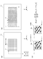
- FIG. 4 is a diagram schematically showing a method of generating a reference template used for the distance detection.
- a flat reflection plane RS perpendicular to the Z-axis direction is arranged at a predetermined distance Ls from the projection optical system 11.
- the temperature of the laser light source 111 is maintained at a predetermined temperature (reference temperature).
- DP light is emitted from the projection optical system 11 for a predetermined time Te.
- the emitted DP light is reflected by the reflection plane RS and enters the CMOS image sensor 123 of the light receiving optical system 12.
- an electrical signal for each pixel is output from the CMOS image sensor 123.
- the output electric signal value (pixel value) for each pixel is developed on the memory 25 of FIG.
- each segment area is dotted with dots in a unique pattern. Therefore, the pixel value pattern of the segment area is different for each segment area.
- each segment area has the same size as all other segment areas.
- the reference template is configured by associating each segment area set on the CMOS image sensor 123 with the pixel value of each pixel included in the segment area.
- the reference template includes information on the position of the reference pattern area on the CMOS image sensor 123, pixel values of all pixels included in the reference pattern area, and information for dividing the reference pattern area into segment areas. Contains.
- the pixel values of all the pixels included in the reference pattern area correspond to the DP light dot pattern included in the reference pattern area.
- the mapping area of the pixel values of all the pixels included in the reference pattern area into segment areas the pixel values of the pixels included in each segment area are acquired.
- the reference template may further hold pixel values of pixels included in each segment area for each segment area.
- the configured reference template is held in the memory 25 of FIG. 2 in an unerasable state.
- the reference template thus stored in the memory 25 is referred to when calculating the distance from the projection optical system 11 to each part of the detection target object.
- DP light corresponding to a predetermined segment area Sn on the reference pattern is reflected by the object, and the segment area Sn. It is incident on a different region Sn ′. Since the projection optical system 11 and the light receiving optical system 12 are adjacent to each other in the X-axis direction, the displacement direction of the region Sn ′ with respect to the segment region Sn is parallel to the X-axis. In the case of FIG. 4A, since the object is located at a position closer than the distance Ls, the region Sn 'is displaced in the X-axis positive direction with respect to the segment region Sn. If the object is at a position farther than the distance Ls, the region Sn ′ is displaced in the negative X-axis direction with respect to the segment region Sn.
- the distance Lr from the projection optical system 11 to the portion of the object irradiated with DP light (DPn) is triangulated using the distance Ls. Calculated based on Similarly, the distance from the projection optical system 11 is calculated for the part of the object corresponding to another segment area.
- FIG. 5 is a diagram for explaining such a detection technique.
- FIG. 5A is a diagram showing the setting state of the reference pattern region and the segment region on the CMOS image sensor 123
- FIG. 5B is a diagram showing a method for searching the segment region at the time of actual measurement
- FIG. These are figures which show the collation method with the dot pattern of measured DP light, and the dot pattern contained in the segment area
- the segment area S1 is one pixel in the X-axis direction in the range P1 to P2.
- the matching degree between the dot pattern of the segment area S1 and the actually measured dot pattern of DP light is obtained.
- the segment area S1 is sent in the X-axis direction only on the line L1 passing through the uppermost segment area group of the reference pattern area. This is because, as described above, each segment region is normally displaced only in the X-axis direction from the position set by the reference template at the time of actual measurement. That is, the segment area S1 is considered to be on the uppermost line L1.
- the processing load for the search is reduced.
- the segment area may protrude from the reference pattern area in the X-axis direction. Therefore, the ranges P1 and P2 are set wider than the width of the reference pattern area in the X-axis direction.
- a region (comparison region) having the same size as the segment region S1 is set on the line L1, and the similarity between the comparison region and the segment region S1 is obtained. That is, the difference between the pixel value of each pixel in the segment area S1 and the pixel value of the corresponding pixel in the comparison area is obtained. A value Rsad obtained by adding the obtained difference to all the pixels in the comparison region is acquired as a value indicating the similarity.
- the comparison area is sequentially set while being shifted by one pixel on the line L1. Then, the value Rsad is obtained for all the comparison regions on the line L1. A value smaller than the threshold value is extracted from the obtained value Rsad. If there is no value Rsad smaller than the threshold value, the search for the segment area S1 is regarded as an error. Then, it is determined that the comparison area corresponding to the extracted Rsad having the smallest value is the movement area of the segment area S1. The same search as described above is performed for the segment areas other than the segment area S1 on the line L1. Similarly, the segment areas on the other lines are searched by setting the comparison area on the lines as described above.
- FIG. 6 is a perspective view showing an installation state of the projection optical system 11 and the light receiving optical system 12.
- the projection optical system 11 and the light receiving optical system 12 are installed on a base plate 300 having high thermal conductivity.
- the optical members constituting the projection optical system 11 are installed on the chassis 11 a, and the chassis 11 a is installed on the base plate 300. Thereby, the projection optical system 11 is installed on the base plate 300.
- the light receiving optical system 12 is installed on the upper surface of the two pedestals 300a on the base plate 300 and the upper surface of the base plate 300 between the two pedestals 300a.
- a CMOS image sensor 123 described later is installed on the upper surface of the base plate 300 between the two pedestals 300a, and a holding plate 12a is installed on the upper surface of the pedestal 300a.
- a lens holder 12b for holding 122 is installed.
- the projection optical system 11 and the light receiving optical system 12 are installed side by side with a predetermined distance in the X axis direction so that the projection center of the projection optical system 11 and the imaging center of the light receiving optical system 12 are aligned on a straight line parallel to the X axis.
- a circuit board 200 (see FIG. 7) that holds the circuit unit (see FIG. 2) of the information acquisition device 1 is installed on the back surface of the base plate 300.
- a hole 300 b for taking out the wiring of the laser light source 111 to the back of the base plate 300 is formed in the lower center of the base plate 300.
- an opening 300 c for exposing the connector 12 c of the CMOS image sensor 123 to the back of the base plate 300 is formed below the installation position of the light receiving optical system 12 on the base plate 300.
- FIG. 7 is a diagram schematically showing the configuration of the projection optical system 11 and the light receiving optical system 12 according to the present embodiment.
- the projection optical system 11 includes a laser light source 111, a collimator lens 112, a rising mirror 113, and a diffractive optical element (DOE: Diffractive Optical Element) 114.
- the light receiving optical system 12 includes a filter 121, an imaging lens 122, and a CMOS image sensor 123.
- the laser light source 111 outputs laser light in a narrow wavelength band with a wavelength of about 830 nm.
- the laser light source 111 is installed so that the optical axis of the laser light is parallel to the X axis.
- the collimator lens 112 converts the laser light emitted from the laser light source 111 into substantially parallel light.
- the collimator lens 112 is installed so that its own optical axis is aligned with the optical axis of the laser light emitted from the laser light source 111.
- the raising mirror 113 reflects the laser beam incident from the collimator lens 112 side.
- the optical axis of the laser beam is bent 90 ° by the rising mirror 113 and becomes parallel to the Z axis.
- the DOE 114 has a diffraction pattern on the incident surface.
- the DOE 114 is formed by injection molding using a resin or using a lithography and dry etching technique on a glass substrate.
- the diffraction pattern is composed of, for example, a step type hologram. Due to the diffractive action of this diffraction pattern, the laser light reflected by the rising mirror 113 and incident on the DOE 114 is converted into a laser light having a dot pattern and irradiated onto the target area.
- the diffraction pattern is designed to be a predetermined dot pattern in the target area. The dot pattern in the target area will be described later with reference to FIGS.
- an aperture (not shown) for making the contour of the laser light circular is arranged between the laser light source 111 and the collimator lens 112. Note that this aperture may be constituted by an emission opening of the laser light source 111.
- the laser light reflected from the target area passes through the filter 121 and enters the imaging lens 122.
- the filter 121 transmits light in a wavelength band including the emission wavelength (about 830 nm) of the laser light source 111 and cuts other wavelength bands.
- the imaging lens 122 condenses the light incident through the filter 121 on the CMOS image sensor 123.
- the imaging lens 122 includes a plurality of lenses, and an aperture and a spacer are interposed between the predetermined lenses. Such an aperture stops the light from the outside so as to match the F number of the imaging lens 122.
- the CMOS image sensor 123 receives the light collected by the imaging lens 122 and outputs a signal (charge) corresponding to the amount of received light to the imaging signal processing circuit 23 for each pixel.
- the output speed of the signal is increased so that the signal (charge) of the pixel can be output to the imaging signal processing circuit 23 with high response from the light reception in each pixel.
- the filter 121 is arranged so that the light receiving surface is perpendicular to the Z axis.
- the imaging lens 122 is installed so that the optical axis is parallel to the Z axis.
- the CMOS image sensor 123 is installed such that the light receiving surface is perpendicular to the Z axis.
- the filter 121, the imaging lens 122, and the CMOS image sensor 123 are arranged so that the center of the filter 121 and the center of the light receiving region of the CMOS image sensor 123 are aligned on the optical axis of the imaging lens 122.
- the projection optical system 11 and the light receiving optical system 12 are installed on the base plate 300 as described with reference to FIG.
- a circuit board 200 is further installed on the lower surface of the base plate 300, and wirings (flexible boards) 201 and 202 are connected from the circuit board 200 to the laser light source 111 and the CMOS image sensor 123.
- the circuit unit of the information acquisition apparatus 1 such as the CPU 21 and the laser driving circuit 22 shown in FIG.
- the DOE 114 is normally designed so that the dots of the dot pattern are uniformly distributed with the same brightness in the target area. By dispersing the dots in this way, it is possible to search the target area evenly.
- the dot pattern is actually generated using the DOE 114 designed in this way, the brightness of the dot differs depending on the region. Moreover, it turned out that there exists a fixed tendency in the difference in the brightness
- analysis and evaluation of DOE 114 performed by the inventors of the present application will be described.
- the inventor of the present application adjusted the diffraction pattern of the DOE 114 as a comparative example so that the dots of the dot pattern are uniformly distributed with the same luminance on the target area. Subsequently, the inventor of the present application actually projected the dot pattern onto the target area using the DOE 114 configured according to such a design, and captured the projected state of the dot pattern at that time with the CMOS image sensor 123. Then, the brightness distribution of the dot pattern on the CMOS image sensor 123 was measured from the received light amount (detection signal) of each pixel of the CMOS image sensor 123.
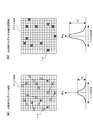
- FIG. 8A shows measurement results showing the luminance distribution on the CMOS image sensor 123 when the DOE 114 of the comparative example is used.
- the central portion of FIG. 8A shows the luminance distribution on the light receiving surface (two-dimensional plane) of the CMOS image sensor 123 by color (in this figure, the luminance difference is represented by the color difference).
- FIG. 8A On the left side and the lower side of FIG. 8A, the luminance values of the portions along the A-A ′ line and the B-B ′ line of the luminance distribution diagram are respectively shown by graphs.
- FIG. 8 (b) is a diagram schematically showing the luminance distribution of FIG. 8 (a).
- the luminance level on the CMOS image sensor 123 is displayed in nine stages, and it can be seen that the luminance decreases from the central part toward the peripheral part.
- the luminance on the CMOS image sensor 123 is maximum at the center and decreases as the distance from the center increases.
- the luminance variation actually occurs on the CMOS image sensor 123. That is, it can be seen from this measurement result that the dot pattern projected onto the target area has a lower dot brightness as it goes from the center to the periphery.
- the luminance of the dots changes radially from the center. That is, it is considered that the dots having substantially the same brightness are distributed in a substantially concentric shape with respect to the center of the dot pattern, and the brightness of the dots gradually decreases with increasing distance from the center.
- the inventors of the present application performed the same measurement as described above for a plurality of DOEs 114 formed in the same manner, this tendency was confirmed in any of the DOEs 114. Therefore, when the DOE 114 is designed so that the dots of the dot pattern are uniformly distributed with the same brightness on the target area, the dots projected on the target area are generally distributed with the above-described tendency. Conceivable.
- the gain of the detection signal in the peripheral portion of the CMOS image sensor 123 can be set large.
- the detection signal based on the stray light also becomes large, and it becomes difficult to properly detect the peripheral dots with low luminance.
- the diffraction pattern of the DOE 114 is adjusted so that the dot pattern is unevenly distributed in the target area.
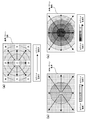
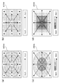
- FIG. 9A is a diagram schematically showing the distribution state of dots in the target area of the present embodiment.
- the DOE 114 according to the present embodiment is configured so that the density of dots in the target area decreases concentrically from the center (in proportion to the distance from the center) by the diffraction action as shown in the figure.
- a portion indicated by a broken line in the figure is a region where the density of dots is substantially equal.
- the dot density may be decreased linearly with increasing distance from the center of the dot pattern, or may be decreased stepwise.
- the dot density is decreased stepwise, as shown in FIGS. 9B and 9C, a plurality of areas are set concentrically from the center of the dot pattern, and the dot density is within each area. Are equal.
- regions having the same dot density are shown with the same darkness.
- the density of dots is reduced by, for example, combining a plurality of dots into one.
- the comparative example it is assumed that 22 dots are included in one segment area (15 pixels ⁇ 15 pixels).
- the brightness of each dot has the brightness B1 schematically shown on the lower side of FIG. From this state, for example, as indicated by a dotted arrow, the design of the DOE 114 is adjusted so that 11 dots are led to positions where they overlap each other 11 dots, respectively.
- FIG. 11B 11 dots are included in one segment area, and the dot density is halved compared to the comparative example. At this time, since each dot in FIG.
- the brightness B2 is about twice as high.
- the brightness is increased while the dot density is reduced.
- the dot superposition as described above is not performed at the center of the dot pattern. Accordingly, the density and brightness of the dot at the center of the dot pattern are the same as in the comparative example.
- the dots in the same segment area are overlapped, but actually, a plurality of dots are overlapped so that the pattern of the dots included in each segment area is a unique pattern, Dot density is reduced. Dots that overlap each other need not be included in the same segment area. In this way, the diffraction pattern of the DOE 114 is adjusted so that the dot pattern of each segment area becomes a unique pattern and the density of dots around the dot pattern is reduced.
- the density of the dots in the peripheral portion is reduced, the luminance in the peripheral portion is increased as described above, so that the dots in the peripheral portion are not easily buried in stray light.
- the number of dots included in the peripheral segment area is smaller than the number of dots included in the central segment area, the pattern matching accuracy of the peripheral segment area may be reduced. is there.
- the diffraction pattern of the DOE 114 is adjusted as shown in FIG. 9A, and the peripheral segment area is set larger than the central segment area.
- FIGS. 11 (a) and 11 (b) are diagrams showing the segment areas in the central part and the peripheral part in the present embodiment, respectively. Also in this embodiment, as in the case of FIGS. 10A and 10B, the density of the dots in the peripheral portion is assumed to be 1 ⁇ 2 of the density of the dots in the central portion.
- the central segment area is set to 15 pixels ⁇ 15 pixels, and one segment area has 22 Contains dots.
- the peripheral segment area is set to 21 pixels ⁇ 21 pixels. Since the density of the peripheral portion is 1 ⁇ 2 of the density of the central portion, here, the area of the peripheral segment region is set so that the area of the peripheral segment region is about twice that of the central segment region. One side is set to 21 pixels, for example. In this case, the number of pixels included in the peripheral segment area is approximately twice the number of pixels included in the central segment area. Accordingly, the number of dots (22) included in the peripheral segment area is equal to the number of dots (22) included in the central segment area.
- the size of the segment area is appropriately set according to the difference in dot density from the center.
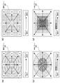
- the segment when the density decreases linearly according to the distance from the central portion, as shown in FIG. 12A, the segment depends on the density of dots on the reference pattern area.
- the size of the area is set to change.
- FIGS. 9B and 9C when the density gradually decreases according to the distance from the center, as shown in FIGS. 12B and 12C, respectively, In accordance with the density of dots on the pattern area, the size of the segment area is set to change stepwise.
- information on the position of the reference pattern area on the CMOS image sensor 123, pixel values of all pixels included in the reference pattern area, information on the vertical and horizontal widths of the segment area, and information on the position of the segment area Is the reference template.
- the reference template of the present embodiment is also held in the memory 25 of FIG.
- the reference template thus stored in the memory 25 is referred to by the CPU 21 when calculating the distance from the projection optical system 11 to each part of the detection target object.
- FIG. 13A is a flowchart showing a dot pattern setting process for a segment area. Such processing is performed when the information acquisition apparatus 1 is activated or when distance detection is started.
- the reference template includes information for assigning individual segment areas whose sizes are adjusted as described above to the reference pattern area (see FIG. 4B). Specifically, the reference template includes information indicating the position of each segment area on the reference pattern area and information indicating the size (vertical and horizontal width) of each segment area.
- N segment areas whose sizes are adjusted with respect to the reference pattern area are allocated, and serial numbers from 1 to N are assigned to these segment areas.
- the CPU 21 of the information acquisition apparatus 1 reads out information on the position of the reference pattern area on the CMOS image sensor 123 and the pixel values of all the pixels included in the reference pattern area from the reference template held in the memory 25 ( S11). Subsequently, the CPU 21 sets 1 to the variable k (S12).
- the CPU 21 acquires information on the vertical and horizontal widths of the k-th segment area Sk and information on the position of the segment area Sk from the reference template stored in the memory 25 (S13). Subsequently, the CPU 21 sets the dot pattern Dk used for the search from the pixel values of all the pixels included in the reference pattern area and the information on the segment area Sk acquired in S13 (S14). Specifically, the CPU 21 acquires the pixel value of the dot pattern included in the segment area Sk among the pixel values of all the pixels of the reference pattern, and sets this as the search dot pattern Dk.
- the CPU 21 determines whether the value of k is equal to N (S15).
- the dot pattern used for the search is set for all the segment areas and the value of k becomes N (S15: YES)
- the process ends.
- the CPU 21 increases the value of k by 1 (S16), and returns the process to S13. In this way, N dot patterns used for the search are sequentially set.
- FIG. 13B is a flowchart showing distance detection processing at the time of actual measurement. This process is performed using the search dot pattern set by the process of FIG. 13A, and is performed in parallel with the process of FIG.
- the CPU 21 of the information acquisition device 1 first sets 1 to the variable c (S21). Next, the CPU 21 searches the dot pattern on the CMOS image sensor 123 received at the time of actual measurement for an area that matches the c-th search dot pattern Dc set in S14 of FIG. 13A (S22). Such a search is performed on an area having a predetermined width in the left-right direction with respect to a position corresponding to the segment area Sc. If there is an area that matches the search dot pattern Dc, the CPU 21 detects how far the matched area has moved in the left or right direction from the position of the segment area Sc, and the detected movement direction and movement. Using the distance, the distance of the object located in the segment area Sc is calculated based on the triangulation method (S23).
- the CPU 21 determines whether the value of c is equal to N (S24). The distance is calculated for all the segment areas, and when the value of c becomes N (S24: YES), the process ends. On the other hand, if the value of c has not reached N (S24: NO), the CPU 21 increases the value of c by 1 (S25), and returns the process to S22. Thus, the distance to the detection target object corresponding to the segment area is obtained.
- the density of the peripheral portion of the dot pattern is set smaller than the density of the central portion.
- the brightness per dot in the peripheral portion is increased, and each dot is less likely to be buried in stray light, making it easier to grasp the position of the dot.
- the peripheral segment region is set larger than the central segment region as shown in FIGS. Is done.
- the CMOS image sensor 123 is used as the photodetector, but a CCD image sensor may be used instead.
- the laser light source 111 and the collimator lens 112 are arranged in the X-axis direction, and the optical axis of the laser beam is bent in the Z-axis direction by the rising mirror 113.
- the laser light source 111 may be arranged so as to emit, and the laser light source 111, the collimator lens 112, and the DOE 114 may be arranged side by side in the Z-axis direction.
- the rising mirror 113 can be omitted, but the dimension of the projection optical system 11 increases in the Z-axis direction.
- the diffraction pattern of the DOE 114 is set so that the density of the dots in the periphery of the dot pattern is 1 ⁇ 2 of the density of the dots in the center. Has been adjusted.
- the present invention is not limited to this, and the density of the dots in the periphery of the dot pattern may be set so that the brightness in the periphery is increased.
- the number of pixels in one segment area is also set to 15 pixels ⁇ 15 pixels in the central portion and 21 pixels ⁇ 21 pixels in the peripheral portion as shown in FIGS. It was done.
- the present invention is not limited to this, and the number of pixels included in the peripheral segment region may be set to another pixel number so as to be larger than the number of pixels included in the central segment region.
- the density of dots in the target area is configured to decrease concentrically as the distance from the center increases.
- an elliptical shape and a rectangular shape may be configured so as to become linearly smaller as the distance from the center increases.
- the density of the dots may be configured to decrease stepwise as they move away radially from the center of the dot pattern.
- the segment area is set by dividing the reference pattern area into a matrix, but the segment area may be set so that the segment areas adjacent to each other on the left and right overlap each other.
- the segment areas may be set so that the segment areas adjacent in the vertical direction overlap each other.
- each segment region is set so that the peripheral portion is larger than the central portion of the dot pattern as described above.
Landscapes
- Physics & Mathematics (AREA)
- Engineering & Computer Science (AREA)
- General Physics & Mathematics (AREA)
- Electromagnetism (AREA)
- Computer Vision & Pattern Recognition (AREA)
- Radar, Positioning & Navigation (AREA)
- Remote Sensing (AREA)
- Computer Networks & Wireless Communication (AREA)
- Measurement Of Optical Distance (AREA)
- Length Measuring Devices By Optical Means (AREA)
Abstract
Description

11 投射光学系
12 受光光学系
21 CPU(距離取得部)
21b 3次元距離演算部(距離取得部)
23 撮像信号処理回路(距離取得部)
111 レーザ光源
112 コリメータレンズ
114 DOE(回折光学素子)
121 フィルタ
122 撮像レンズ(集光レンズ)
123 CMOSイメージセンサ(撮像素子)
Claims (6)
- 光を用いて目標領域の情報を取得する情報取得装置において、
前記目標領域に所定のドットパターンでレーザ光を投射する投射光学系と、
前記投射光学系に対して所定の距離だけ離れて並ぶように配置され、前記目標領域を撮像する受光光学系と、
前記受光光学系により撮像された前記ドットパターンに基づいて目標領域に存在する物体の各部までの距離を取得する距離取得部と、を備え、
前記投射光学系は、前記目標領域における前記ドットパターンのドットの密度が、前記ドットパターンの中心部よりも周辺部の方が小さくなるよう構成され、
前記距離取得部は、基準面により反射され前記受光光学系により撮像された基準ドットパターンをセグメント領域に区分し、距離測定時に目標領域を撮像して取得された撮像ドットパターンと前記各セグメント領域内のドットとを照合することにより、前記各セグメント領域についての距離を取得し、
前記セグメント領域は、前記基準ドットパターンの中心部よりも周辺部の方が大きくなるよう設定される、
ことを特徴とする情報取得装置。 - 請求項1に記載の情報取得装置において、
前記投射光学系は、前記基準面における前記ドットの密度が、前記基準ドットパターンの中心からの距離に応じて小さくなるよう構成され、
前記セグメント領域は、前記基準ドットパターンの中心から距離に応じて大きくなるよう構成される、
ことを特徴とする情報取得装置。 - 請求項2に記載の情報取得装置において、
前記投射光学系は、前記基準面における前記ドットの密度が、前記基準ドットパターンの中心から放射状に離れるに従って段階的に小さくなるよう構成され、
前記セグメント領域は、前記基準ドットパターンの中心から放射状に離れるに従って段階的に大きくなるよう構成される、
ことを特徴とする情報取得装置。 - 請求項1ないし3の何れか一項に記載の情報取得装置において、
前記投射光学系は、前記基準面における前記ドットの輝度が、前記基準ドットパターンの中心部よりも周辺部の方が高くなるよう構成されている、
ことを特徴とする情報取得装置。 - 請求項1ないし4の何れか一項に記載の情報取得装置において、
前記投射光学系は、
レーザ光源と、
前記レーザ光源から出射されたレーザ光が入射するコリメータレンズと、
前記コリメータレンズを透過した前記レーザ光を回折によりドットパターンの光に変換する回折光学素子と、を備え、
前記受光光学系は、
撮像素子と、
目標領域からの前記レーザ光を前記撮像素子に集光する集光レンズと、
前記レーザ光の波長帯域の光を抽出して前記撮像素子に導くためのフィルタと、を備える、
ことを特徴とする情報取得装置。 - 請求項1ないし5の何れか一項に記載の情報取得装置を有する物体検出装置。
Priority Applications (3)
| Application Number | Priority Date | Filing Date | Title |
|---|---|---|---|
| CN2012800006045A CN102859319A (zh) | 2011-04-19 | 2012-04-06 | 信息获取装置以及物体检测装置 |
| JP2012525802A JP5138116B2 (ja) | 2011-04-19 | 2012-04-06 | 情報取得装置および物体検出装置 |
| US13/614,825 US20130002859A1 (en) | 2011-04-19 | 2012-09-13 | Information acquiring device and object detecting device |
Applications Claiming Priority (2)
| Application Number | Priority Date | Filing Date | Title |
|---|---|---|---|
| JP2011092927 | 2011-04-19 | ||
| JP2011-092927 | 2011-04-19 |
Related Child Applications (1)
| Application Number | Title | Priority Date | Filing Date |
|---|---|---|---|
| US13/614,825 Continuation US20130002859A1 (en) | 2011-04-19 | 2012-09-13 | Information acquiring device and object detecting device |
Publications (1)
| Publication Number | Publication Date |
|---|---|
| WO2012144339A1 true WO2012144339A1 (ja) | 2012-10-26 |
Family
ID=47041451
Family Applications (1)
| Application Number | Title | Priority Date | Filing Date |
|---|---|---|---|
| PCT/JP2012/059446 Ceased WO2012144339A1 (ja) | 2011-04-19 | 2012-04-06 | 情報取得装置および物体検出装置 |
Country Status (4)
| Country | Link |
|---|---|
| US (1) | US20130002859A1 (ja) |
| JP (1) | JP5138116B2 (ja) |
| CN (1) | CN102859319A (ja) |
| WO (1) | WO2012144339A1 (ja) |
Cited By (3)
| Publication number | Priority date | Publication date | Assignee | Title |
|---|---|---|---|---|
| WO2016056628A1 (ja) * | 2014-10-09 | 2016-04-14 | シャープ株式会社 | 画像認識処理装置及びプログラム |
| JP2017020971A (ja) * | 2015-07-14 | 2017-01-26 | 株式会社リコー | パターン画像投射装置、視差情報生成装置、パターン画像生成プログラム |
| JPWO2019009260A1 (ja) * | 2017-07-03 | 2020-04-30 | 大日本印刷株式会社 | 回折光学素子、光照射装置、照射パターンの読取り方法 |
Families Citing this family (8)
| Publication number | Priority date | Publication date | Assignee | Title |
|---|---|---|---|---|
| DE102013200657B4 (de) * | 2013-01-17 | 2015-11-26 | Sypro Optics Gmbh | Vorrichtung zur Erzeugung eines optischen Punktmusters |
| US9361698B1 (en) * | 2014-11-12 | 2016-06-07 | Amazon Technologies, Inc. | Structure light depth sensor |
| DE112015006245B4 (de) * | 2015-03-30 | 2019-05-23 | Fujifilm Corporation | Abstandsbild-Erfassungsvorrichtung und Abstandsbild-Erfassungsverfahren |
| KR101850139B1 (ko) * | 2016-06-29 | 2018-04-19 | 주식회사 크리에이츠 | 공 이미지의 밝기를 보정하기 위한 방법, 시스템 및 비일시성의 컴퓨터 판독 가능한 기록 매체 |
| US11629949B2 (en) * | 2018-04-20 | 2023-04-18 | Qualcomm Incorporated | Light distribution for active depth systems |
| CN109188357B (zh) * | 2018-08-28 | 2023-04-14 | 上海宽创国际文化科技股份有限公司 | 一种基于结构光阵列的室内定位系统和方法 |
| CN109597530B (zh) * | 2018-11-21 | 2022-04-19 | 深圳闳宸科技有限公司 | 显示设备及屏幕定位方法 |
| CN110375736B (zh) * | 2018-11-28 | 2021-02-26 | 北京京东尚科信息技术有限公司 | 智能设备的路径规划方法、系统、设备及可读存储介质 |
Citations (7)
| Publication number | Priority date | Publication date | Assignee | Title |
|---|---|---|---|---|
| JP2000292133A (ja) * | 1999-04-02 | 2000-10-20 | Nippon Steel Corp | パターン投影装置 |
| JP2000292135A (ja) * | 1999-04-07 | 2000-10-20 | Minolta Co Ltd | 3次元情報入力カメラ |
| JP2004191092A (ja) * | 2002-12-09 | 2004-07-08 | Ricoh Co Ltd | 3次元情報取得システム |
| JP2006061222A (ja) * | 2004-08-24 | 2006-03-09 | Sumitomo Osaka Cement Co Ltd | 動き検出装置 |
| JP2009014712A (ja) * | 2007-06-07 | 2009-01-22 | Univ Of Electro-Communications | 物体検出装置とそれを適用したゲート装置 |
| JP2009270915A (ja) * | 2008-05-07 | 2009-11-19 | Kagawa Univ | 3次元形状の計測方法および装置 |
| JP2010101683A (ja) * | 2008-10-22 | 2010-05-06 | Nissan Motor Co Ltd | 距離計測装置および距離計測方法 |
Family Cites Families (18)
| Publication number | Priority date | Publication date | Assignee | Title |
|---|---|---|---|---|
| JP2527403B2 (ja) * | 1993-10-08 | 1996-08-21 | 岸本産業株式会社 | レ―ザ光を利用したスペックルパタ―ンによる被計測物の移動量の修正方法ならびにその装置 |
| JP3556589B2 (ja) * | 2000-09-20 | 2004-08-18 | ファナック株式会社 | 位置姿勢認識装置 |
| JP3704706B2 (ja) * | 2002-03-13 | 2005-10-12 | オムロン株式会社 | 三次元監視装置 |
| CN1203292C (zh) * | 2003-08-15 | 2005-05-25 | 清华大学 | 测量物体三维表面轮廊的方法 |
| JP3960295B2 (ja) * | 2003-10-31 | 2007-08-15 | 住友電気工業株式会社 | チルト誤差低減非球面ホモジナイザー |
| JP4577126B2 (ja) * | 2005-07-08 | 2010-11-10 | オムロン株式会社 | ステレオ対応づけのための投光パターンの生成装置及び生成方法 |
| US20110044544A1 (en) * | 2006-04-24 | 2011-02-24 | PixArt Imaging Incorporation, R.O.C. | Method and system for recognizing objects in an image based on characteristics of the objects |
| WO2007138904A1 (ja) * | 2006-05-30 | 2007-12-06 | Panasonic Corporation | パターン投影光源および複眼測距装置 |
| US8724013B2 (en) * | 2007-12-27 | 2014-05-13 | Qualcomm Incorporated | Method and apparatus with fast camera auto focus |
| US8384997B2 (en) * | 2008-01-21 | 2013-02-26 | Primesense Ltd | Optical pattern projection |
| JP2009200683A (ja) * | 2008-02-20 | 2009-09-03 | Seiko Epson Corp | 画像処理装置、プロジェクタ、歪み補正方法 |
| WO2010023442A2 (en) * | 2008-08-26 | 2010-03-04 | The University Court Of The University Of Glasgow | Uses of electromagnetic interference patterns |
| GB0921461D0 (en) * | 2009-12-08 | 2010-01-20 | Qinetiq Ltd | Range based sensing |
| US8320621B2 (en) * | 2009-12-21 | 2012-11-27 | Microsoft Corporation | Depth projector system with integrated VCSEL array |
| DE102010001357A1 (de) * | 2010-01-29 | 2011-08-04 | Bremer Institut für angewandte Strahltechnik GmbH, 28359 | Vorrichtung zur laseroptischen Erzeugung von mechanischen Wellen zur Bearbeitung und/oder Untersuchung eines Körpers |
| US8558873B2 (en) * | 2010-06-16 | 2013-10-15 | Microsoft Corporation | Use of wavefront coding to create a depth image |
| US20120056982A1 (en) * | 2010-09-08 | 2012-03-08 | Microsoft Corporation | Depth camera based on structured light and stereo vision |
| US8836761B2 (en) * | 2010-09-24 | 2014-09-16 | Pixart Imaging Incorporated | 3D information generator for use in interactive interface and method for 3D information generation |
-
2012
- 2012-04-06 WO PCT/JP2012/059446 patent/WO2012144339A1/ja not_active Ceased
- 2012-04-06 JP JP2012525802A patent/JP5138116B2/ja not_active Expired - Fee Related
- 2012-04-06 CN CN2012800006045A patent/CN102859319A/zh active Pending
- 2012-09-13 US US13/614,825 patent/US20130002859A1/en not_active Abandoned
Patent Citations (7)
| Publication number | Priority date | Publication date | Assignee | Title |
|---|---|---|---|---|
| JP2000292133A (ja) * | 1999-04-02 | 2000-10-20 | Nippon Steel Corp | パターン投影装置 |
| JP2000292135A (ja) * | 1999-04-07 | 2000-10-20 | Minolta Co Ltd | 3次元情報入力カメラ |
| JP2004191092A (ja) * | 2002-12-09 | 2004-07-08 | Ricoh Co Ltd | 3次元情報取得システム |
| JP2006061222A (ja) * | 2004-08-24 | 2006-03-09 | Sumitomo Osaka Cement Co Ltd | 動き検出装置 |
| JP2009014712A (ja) * | 2007-06-07 | 2009-01-22 | Univ Of Electro-Communications | 物体検出装置とそれを適用したゲート装置 |
| JP2009270915A (ja) * | 2008-05-07 | 2009-11-19 | Kagawa Univ | 3次元形状の計測方法および装置 |
| JP2010101683A (ja) * | 2008-10-22 | 2010-05-06 | Nissan Motor Co Ltd | 距離計測装置および距離計測方法 |
Cited By (4)
| Publication number | Priority date | Publication date | Assignee | Title |
|---|---|---|---|---|
| WO2016056628A1 (ja) * | 2014-10-09 | 2016-04-14 | シャープ株式会社 | 画像認識処理装置及びプログラム |
| JP2017020971A (ja) * | 2015-07-14 | 2017-01-26 | 株式会社リコー | パターン画像投射装置、視差情報生成装置、パターン画像生成プログラム |
| JPWO2019009260A1 (ja) * | 2017-07-03 | 2020-04-30 | 大日本印刷株式会社 | 回折光学素子、光照射装置、照射パターンの読取り方法 |
| JP7488652B2 (ja) | 2017-07-03 | 2024-05-22 | 大日本印刷株式会社 | 回折光学素子、光照射装置、照射パターンの読取り方法 |
Also Published As
| Publication number | Publication date |
|---|---|
| JPWO2012144339A1 (ja) | 2014-07-28 |
| CN102859319A (zh) | 2013-01-02 |
| US20130002859A1 (en) | 2013-01-03 |
| JP5138116B2 (ja) | 2013-02-06 |
Similar Documents
| Publication | Publication Date | Title |
|---|---|---|
| JP5138116B2 (ja) | 情報取得装置および物体検出装置 | |
| WO2012137674A1 (ja) | 情報取得装置、投射装置および物体検出装置 | |
| JP5143312B2 (ja) | 情報取得装置、投射装置および物体検出装置 | |
| JP5214062B1 (ja) | 情報取得装置および物体検出装置 | |
| JP5138119B2 (ja) | 物体検出装置および情報取得装置 | |
| JP5138115B2 (ja) | 情報取得装置及びその情報取得装置を有する物体検出装置 | |
| JP2012237604A (ja) | 情報取得装置、投射装置および物体検出装置 | |
| JP2014238259A (ja) | 情報取得装置および物体検出装置 | |
| JPWO2013015145A1 (ja) | 情報取得装置および物体検出装置 | |
| JP5143314B2 (ja) | 情報取得装置および物体検出装置 | |
| WO2012144340A1 (ja) | 情報取得装置および物体検出装置 | |
| WO2013046928A1 (ja) | 情報取得装置および物体検出装置 | |
| WO2013015146A1 (ja) | 物体検出装置および情報取得装置 | |
| JP2014085257A (ja) | 情報取得装置および物体検出装置 | |
| WO2013031447A1 (ja) | 物体検出装置および情報取得装置 | |
| WO2013031448A1 (ja) | 物体検出装置および情報取得装置 | |
| JP5138120B2 (ja) | 物体検出装置および情報取得装置 | |
| JP2014035304A (ja) | 情報取得装置および物体検出装置 | |
| JP2013234956A (ja) | 情報取得装置および物体検出装置 | |
| JP2014085282A (ja) | 情報取得装置および物体検出装置 | |
| JP2014098585A (ja) | 情報取得装置および物体検出装置 |
Legal Events
| Date | Code | Title | Description |
|---|---|---|---|
| WWE | Wipo information: entry into national phase |
Ref document number: 201280000604.5 Country of ref document: CN |
|
| ENP | Entry into the national phase |
Ref document number: 2012525802 Country of ref document: JP Kind code of ref document: A |
|
| 121 | Ep: the epo has been informed by wipo that ep was designated in this application |
Ref document number: 12774491 Country of ref document: EP Kind code of ref document: A1 |
|
| NENP | Non-entry into the national phase |
Ref country code: DE |
|
| 122 | Ep: pct application non-entry in european phase |
Ref document number: 12774491 Country of ref document: EP Kind code of ref document: A1 |