WO2012147309A1 - Elément de charge, cartouche de traitement et dispositif photographique électronique - Google Patents
Elément de charge, cartouche de traitement et dispositif photographique électronique Download PDFInfo
- Publication number
- WO2012147309A1 WO2012147309A1 PCT/JP2012/002686 JP2012002686W WO2012147309A1 WO 2012147309 A1 WO2012147309 A1 WO 2012147309A1 JP 2012002686 W JP2012002686 W JP 2012002686W WO 2012147309 A1 WO2012147309 A1 WO 2012147309A1
- Authority
- WO
- WIPO (PCT)
- Prior art keywords
- group
- general formula
- carbon atoms
- charging member
- independently
- Prior art date
- Legal status (The legal status is an assumption and is not a legal conclusion. Google has not performed a legal analysis and makes no representation as to the accuracy of the status listed.)
- Ceased
Links
Images



Classifications
-
- G—PHYSICS
- G03—PHOTOGRAPHY; CINEMATOGRAPHY; ANALOGOUS TECHNIQUES USING WAVES OTHER THAN OPTICAL WAVES; ELECTROGRAPHY; HOLOGRAPHY
- G03G—ELECTROGRAPHY; ELECTROPHOTOGRAPHY; MAGNETOGRAPHY
- G03G15/00—Apparatus for electrographic processes using a charge pattern
- G03G15/02—Apparatus for electrographic processes using a charge pattern for laying down a uniform charge, e.g. for sensitising; Corona discharge devices
-
- G—PHYSICS
- G03—PHOTOGRAPHY; CINEMATOGRAPHY; ANALOGOUS TECHNIQUES USING WAVES OTHER THAN OPTICAL WAVES; ELECTROGRAPHY; HOLOGRAPHY
- G03G—ELECTROGRAPHY; ELECTROPHOTOGRAPHY; MAGNETOGRAPHY
- G03G15/00—Apparatus for electrographic processes using a charge pattern
- G03G15/02—Apparatus for electrographic processes using a charge pattern for laying down a uniform charge, e.g. for sensitising; Corona discharge devices
- G03G15/0208—Apparatus for electrographic processes using a charge pattern for laying down a uniform charge, e.g. for sensitising; Corona discharge devices by contact, friction or induction, e.g. liquid charging apparatus
- G03G15/0216—Apparatus for electrographic processes using a charge pattern for laying down a uniform charge, e.g. for sensitising; Corona discharge devices by contact, friction or induction, e.g. liquid charging apparatus by bringing a charging member into contact with the member to be charged, e.g. roller, brush chargers
- G03G15/0233—Structure, details of the charging member, e.g. chemical composition, surface properties
Definitions
- the present invention relates to a charging member, process cartridge, and electrophotographic apparatus used for contact charging of an electrophotographic apparatus.
- the charging member that contacts the electrophotographic photosensitive member to charge the electrophotographic photosensitive member generally has an elastic layer containing rubber in order to ensure a sufficient and uniform contact nip between the electrophotographic photosensitive member and the charging member.
- this elastic layer inevitably contains a low molecular weight component, the low molecular weight component may ooze out on the surface of the charging member due to long-term use, and may contaminate the surface of the electrophotographic photosensitive member. .
- Patent Document 1 has a configuration in which the peripheral surface of the elastic layer is covered with an inorganic oxide coating or an inorganic-organic hybrid coating to prevent low molecular weight components from seeping out on the surface of the charging member. Proposed.
- the charging member when charging the surface of the electrophotographic photosensitive member, the charging member is in an environment where the surface is easily oxidized. Therefore, when the charging member is used for a long period of time, the surface of the charging member may be oxidized and gradually deteriorated, and the charging performance may change over time.
- an object of the present invention is to provide a charging member that is excellent in charging performance of an electrophotographic photosensitive member and that is less likely to change with time.
- Another object of the present invention is to provide an electrophotographic apparatus and a process cartridge capable of stably forming a high-quality electrophotographic image.
- a charging member for electrophotography having a substrate, an elastic layer, and a surface layer, the surface layer comprising a polymer compound having a Si—O—Ti bond in the molecular structure
- a charging member for an electrophotographic apparatus comprising a cyclic polysilane represented by the general formula (7), wherein the polymer compound has a structural unit represented by the following general formula (1) and a structural unit represented by the following formula (2): Is provided.
- R 3 to R 7 , R 10 to R 14 , R 19 , R 20 , R 25 and R 26 are each independently a hydrogen atom, a straight chain having 1 to 4 carbon atoms. A chain or branched alkyl group, a hydroxyl group, a carboxyl group, or an amino group is shown.
- R 8 , R 9 , R 15 to R 18 , R 23 , R 24 , and R 29 to R 32 are each independently a hydrogen atom or a linear or branched alkyl group having 1 to 4 carbon atoms. Show.
- R 21 , R 22 , R 27 , and R 28 each independently represent a hydrogen atom, an alkoxy group having 1 to 4 carbon atoms, or a linear or branched alkyl group having 1 to 4 carbon atoms.
- n1, m1, q1, s1, t1, and v1 each independently represents an integer of 1 to 8
- p1 and r1 each independently represents an integer of 4 to 12
- x1 and y1 each independently represents 0 or 1 Indicates.
- * And ** each represent a bonding position with a silicon atom and an oxygen atom in the general formula (1). ].
- R ⁇ and R ⁇ each independently represent a hydrogen atom, hydroxyl group, alkyl group, alkoxy group, alkenyl group, cycloalkyl group, cycloalkyloxy group, cycloalkenyl group, aryl group, aryloxy group. Or a silyl group.
- u1 represents an integer of 4 or more and 12 or less.
- an electrophotographic apparatus having an electrophotographic photosensitive member and the charging member disposed in contact with the electrophotographic photosensitive member.
- a process cartridge having an electrophotographic photosensitive member and the charging member arranged in contact with the electrophotographic photosensitive member and detachably mounted on the electrophotographic apparatus.
- the present invention it is possible to obtain a charging member which is excellent in charging performance and whose charging performance hardly changes over time.
- an electrophotographic apparatus and a process cartridge capable of stably forming a high-quality electrophotographic image can be obtained.
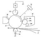
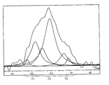
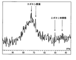
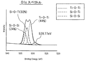
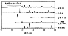
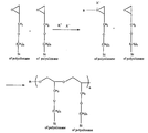
- FIG. 1 is a schematic diagram of an example of an electrophotographic apparatus according to the present invention. It is a figure which shows the measurement result of 29 Si-NMR of a high molecular compound. It is a figure which shows the measurement result of 13 C-NMR of a high molecular compound. It is a figure which shows the measurement result by ESCA of the surface layer of the charging member which concerns on this invention. It is a figure which shows the measurement result by ESCA of the surface layer of the charging member which concerns on this invention. It is a figure which shows the measurement result in XRD of the surface layer of the charging member which concerns on this invention. It is a figure which shows the measurement result in XRD of the surface layer of the charging member which concerns on this invention. It is explanatory drawing regarding the crosslinking reaction at the time of forming a surface layer.
- the charging member according to the present invention includes a polymer compound described later and cyclic polysilane. Further, the charging member of the present invention can have a surface layer containing a polymer compound and cyclic polysilane. As shown in FIG. 1, the base 101, the conductive elastic layer 102, and the surface layer 103 are formed of the surface layer. It can be set as the structure laminated
- the charging member for an electrophotographic apparatus of the present invention can be used in a belt shape (charging belt), a blade shape (charging blade), or a brush shape (charging brush) in addition to the charging roller having the above-described roller shape.
- a metallic (alloy) substrate for example, a columnar metal formed of iron, copper, stainless steel, aluminum, aluminum alloy, or nickel can be used.
- the elastic layer a conventional elastic layer of a charging member for an electrophotographic apparatus can be used.
- one or more elastic bodies such as rubber and thermoplastic elastomer described later can be used.
- the rubber include the following. Urethane rubber, silicone rubber, butadiene rubber, isoprene rubber, chloroprene rubber, styrene-butadiene rubber, ethylene-propylene rubber, styrene-butadiene-styrene rubber, acrylonitrile rubber, epichlorohydrin rubber and alkyl ether rubber.
- the following are mentioned as a thermoplastic elastomer. Styrene elastomer and olefin elastomer.
- the elastic layer can be configured as a conductive elastic layer having a predetermined conductivity by including a conductive agent in addition to the above-described rubber and thermoplastic elastomer.
- the electric resistance value of the elastic layer is preferably 10 2 ⁇ to 10 8 ⁇ , more preferably 10 3 ⁇ to 10 6 ⁇ .
- the conductive agent used in the elastic layer include a cationic surfactant, an anionic surfactant, an antistatic agent, and an electrolyte.
- cationic surfactants include the following. Quaternary ammonium salts (such as lauryltrimethylammonium, stearyltrimethylammonium, octadodecyltrimethylammonium, dodecyltrimethylammonium, hexadecyltrimethylammonium, and modified fatty acid / dimethylethylammonium), perchlorate, chlorate, borohydrofluoric acid Salts, ethosulphate salts and benzyl halide salts (such as benzyl bromide and benzyl chloride).
- anionic surfactant include the following. Aliphatic sulfonates, higher alcohol sulfates, higher alcohol ethylene oxide addition sulfates, higher alcohol phosphates, higher alcohol ethylene oxide addition phosphates, and the like.
- Examples of the antistatic agent include nonionic antistatic agents such as higher alcohol ethylene oxide, polyethylene glycol fatty acid ester and polyhydric alcohol fatty acid ester.
- Examples of the electrolyte include salts (such as quaternary ammonium salts) of metals (Li, Na, K, etc.) belonging to Group 1 of the periodic table. Specific examples of the metal salt of Group 1 of the periodic table include LiCF 3 SO 3 , NaClO 4 , LiAsF 6 , LiBF 4 , NaSCN, KSCN, and NaCl.
- a salt (Ca (ClO 4 ) 2 or the like) of a metal (Ca, Ba, etc.) belonging to Group 2 of the periodic table or an antistatic agent derived therefrom can be used.
- complexes thereof with polyhydric alcohols (1,4-butanediol, ethylene glycol, polyethylene glycol, propylene glycol, polyethylene glycol, etc.) or derivatives thereof, and monools (ethylene glycol monomethyl ether, ethylene glycol monoethyl ether) Etc.) can be used.
- carbon-based materials such as conductive carbon black and graphite
- metal oxides such as tin oxide, titanium oxide, and zinc oxide
- metals such as nickel, copper, silver, and germanium
- the hardness of the elastic layer is 60 degrees or more and 85 degrees or less in MD-1 from the viewpoint of suppressing deformation of the charging member when the charging member and the electrophotographic photosensitive member as the charged body are brought into contact with each other. It is preferably 70 degrees or more and 80 degrees or less.
- the MD-1 hardness is measured by bringing the MD-1 hardness tester (manufactured by Kobunshi Keiki Co., Ltd.) into contact with the surface of the measurement object in a measurement environment of 25 ° C. ⁇ 55% RH (relative humidity). It can be carried out.
- the elastic layer preferably has a so-called crown shape in which the layer thickness at the center in the width direction is thicker than the layer thickness at the end.
- the surface layer of the charging member according to the present invention is represented by a polymer compound having a Si—O—Ti bond in the molecular structure (hereinafter sometimes simply referred to as a polymer compound) and a general formula (7) described later. Cyclic polysilane.
- Polymer compound used in the present invention has a Si—O—Ti bond in the molecular structure, a structural unit represented by the following general formula (1), and a structural unit represented by the following formula (2) Have both.
- Formula (2) TiO 4/2 [In general formula (1), R 1 and R 2 each independently represents any one selected from the structures represented by the following general formulas (3) to (6)).
- R 3 to R 7 , R 10 to R 14 , R 19 , R 20 , R 25 and R 26 are each independently a hydrogen atom, a straight chain having 1 to 4 carbon atoms. Or a branched alkyl group, a hydroxyl group, a carboxyl group, or an amino group.
- R 8 , R 9 , R 15 to R 18 , R 23 , R 24 and R 29 to R 32 each independently represent a hydrogen atom or a linear or branched alkyl group having 1 to 4 carbon atoms.
- R 21 , R 22 , R 27 and R 28 each independently represent a hydrogen atom, an alkoxy group having 1 to 4 carbon atoms, or a linear or branched alkyl group having 1 to 4 carbon atoms.
- At least one of CR 8 R 9 , CR 15 R 16 , CR 17 R 18 , CR 23 R 24 , CR 29 R 30 , and CR 31 R 32 may be a carbonyl group.
- At least one pair selected from the group consisting of the following groups may be bonded to each other to form a ring structure.
- R 3 and R 4 , R 6 and R 7 , R 10 and R 11 , R 13 and R 14 , R 3 , R 4 , R 6 and R 7 A set of any one and R 5 ; a set of any one of R 10 , R 11 , R 13 and R 14 and R 12 ; a set of R 5 and a carbon atom in (CR 8 R 9 ) n1 ; And a combination of R 12 and a carbon atom in (CR 15 R 16 ) m1 .
- N1, m1, q1, s1, t1, and v1 each independently represents an integer of 1 or more and 8 or less.
- p1 and r1 each independently represents an integer of 4 or more and 12 or less.
- x1 and y1 each independently represent 0 or 1.
- * and ** each represent a bonding position with a silicon atom and an oxygen atom in the general formula (1).
- R 1 in the general formula (1) is the structure represented by the general formula (3) and R 2 is the structure represented by the general formula (4).
- R 1 in the general formula (1) is the structure represented by the general formula (3)
- R 2 is the structure represented by the general formula (4).
- An example of a part is shown.
- R 1 in the general formula (1) is the structure represented by the general formula (3) and R 2 is the structure represented by the general formula (6) Some examples are shown.
- the polymer compound used in the present invention has a constitutional unit represented by the general formula (1) and can have a structure in which an organic chain portion bonded to a siloxane bond and Si is polymerized with each other. Can be large. SiO 3/2 means that Si is three-dimensionally cross-linked.
- the surface layer containing the polymer compound used in the present invention is dense and can suppress bleeding of low molecular weight components from the conductive elastic layer.
- the surface layer can contain an inorganic compound having the structural unit TiO 4/2 represented by the formula (2), the surface layer can have an excellent charging ability that can cope with an increase in the speed of the electrophotographic process.
- the structure represented by the formula (2) can be formed by preparing a polymer compound using a titanium compound having a high relative dielectric constant as a metal oxide. That is, TiO 4/2 can have a structure derived from titanium oxide. TiO 4/2 means that all four reaction points of Ti are in a reaction state.
- the Si—O—Ti bond can be composed of SiO 3/2 in the general formula (1) and TiO 4/2 in the formula (2).
- the charging ability of the surface layer can be adjusted by adjusting the kind and amount of the organic chain bonded to the Si atom.
- an oxide is used as the Ti raw material for this polymer compound, it is preferable to use an oxide that does not have a complete crystal structure (rutile type, anatase type). Thereby, suppression of sedimentation and aggregation becomes easy and it can be set as the coating material excellent in stability.
- FIG. 6A shows the result of observing the surface of an example of the charging member of the present invention containing CaCO 3 and ZnO 2 in the conductive elastic layer with an X-ray apparatus (trade name: RINT TTRII, manufactured by Rigaku).
- RINT TTRII X-ray apparatus
- R 1 and R 2 in the general formula (1) are each independently selected from structures represented by the following general formulas (8) to (11), respectively. It is preferable. With such a structure, the surface layer can be made stronger and more durable.
- the structure containing an ether group represented by each of the following general formulas (9) and (11) is particularly preferable because the adhesion of the surface layer to the elastic body layer can be further improved.
- n2, m2, q2, s2, t2, and v2 each independently represent an integer of 1 or more and 8 or less, and x2 and y2 each independently represent 0 or 1. Further, * and ** each represent a bonding position with a silicon atom and an oxygen atom in the general formula (1).
- the atomic ratio (Ti / Si) of titanium and silicon in the polymer compound is preferably 0.1 or more and 12.5 or less. Thereby, the charging capability of the charging member can be easily improved.
- the polymer compound used in the present invention is a cross-linked product (first compound) of a hydrolyzable compound having a structure represented by the following general formula (12) and a hydrolyzable compound represented by the following general formula (13).
- Cross-linked product is preferred.
- the first cross-linked product is a hydrolyzed condensate (first product) obtained by subjecting a hydrolyzable compound represented by the general formula (12) and a hydrolyzable compound represented by the general formula (13) to a hydrolysis and condensation reaction.
- 1 condensate) can be obtained by polymerization (crosslinking).
- the first condensates are cross-linked by the polymerization of the R 33 epoxy group portions of the general formula (12).
- ultraviolet rays can be used for crosslinking.
- R 33 represents any one selected from the structures represented by the following general formulas (14) to (17) each having an epoxy group.
- R 34 to R 36 each independently represents a linear or branched alkyl group having 1 to 4 carbon atoms.
- R 41 to R 43 , R 46 to R 48 , R 53 , R 54 , R 59 and R 60 are each independently a hydrogen atom, a straight chain having 1 to 4 carbon atoms. Or a branched alkyl group, a hydroxyl group, a carboxyl group, or an amino group.
- R 44 , R 45 , R 49 to R 52 , R 57 , R 58 and R 63 to R 66 each independently represent a hydrogen atom or a linear or branched alkyl group having 1 to 4 carbon atoms. .
- R 55 , R 56 , R 61 and R 62 each independently represent a hydrogen atom, an alkoxy group having 1 to 4 carbon atoms, or a linear or branched alkyl group having 1 to 4 carbon atoms. *** indicates a bonding position with the silicon atom in the general formula (12).
- CR 44 R 45 , CR 49 R 50 , CR 51 R 52 , CR 57 R 58 , CR 63 R 64 and CR 65 R 66 may be a carbonyl group.
- At least one group selected from the group consisting of the following groups may be bonded to each other to form a ring to form a cycloalkane.
- (CR 44 R 45 ) a group consisting of at least any two of carbon atoms in R 3 , R 41 , R 42 and R 43 , (CR 49 R 50 ) carbon atoms in m 3 , R 46 , R 47 and at least one group consists of two of R 48, the set of R 53 and R 54, as well as a set of R 59 and R 60.
- N3, m3, q3, s3, t3 and v3 each independently represents an integer of 1 to 8
- p3 and r3 each independently represents an integer of 4 to 12.
- hydrolyzable silane compound (component A) having the structure represented by the general formula (12) are shown below.
- A-1) 4- (1,2-epoxybutyl) trimethoxysilane (A-2) 5,6-epoxyhexyltriethoxysilane (A-3) 8-oxiran-2-yloctyltrimethoxysilane (A -4) 8-oxiran-2-yloctyltriethoxysilane (A-5) 3-glycidoxypropyltrimethoxysilane (A-6) 3-glycidoxypropyltriethoxysilane (A-7) 1- ( 3,4-epoxycyclohexyl) ethyltrimethoxysilane (A-8) 1- (3,4-epoxycyclohexyl) ethyltriethoxysilane (A-9) 3- (3,4-epoxycyclohexyl) methyloxypropyltrimethoxy Silane (A-10) 3- (3,4
- R 37 to R 40 each independently represents a linear or branched alkyl group having 1 to 9 carbon atoms.
- the polymer compound used in the present invention is represented by the hydrolyzable compound represented by the general formula (12), the hydrolyzable compound represented by the general formula (13), and the following general formula (18).
- a cross-linked product (second cross-linked product) with a hydrolyzable compound is preferable.
- the electrical properties can be easily improved as the solubility and coating properties of the general formulas (12) and (13) at the synthesis stage, and the film physical properties after curing, which is preferable.
- the second cross-linked product is obtained by subjecting the hydrolyzable compound of the general formula (12), the hydrolyzable compound of the general formula (13), and the hydrolyzable compound of the general formula (18) to a hydrolysis and condensation reaction.
- the obtained hydrolysis condensate (second condensate) can be obtained by polymerization (crosslinking).
- R 67 represents a linear or branched alkyl group having 1 to 4 carbon atoms or a phenyl group
- R 68 to R 70 each independently has 1 to 6 carbon atoms.
- a linear or branched alkyl group is shown.
- R67 is an alkyl group
- solubility and coating properties can be improved, which is preferable.
- R 67 is a phenyl group, it contributes to improvement of electrical characteristics, particularly volume resistivity, which is preferable.
- the surface layer used in the present invention contains cyclic polysilane represented by the following general formula (7) in addition to the polymer compound.
- cyclic polysilane compound represented by the following general formula (7) in addition to the polymer compound.
- R ⁇ and R ⁇ each independently represent a hydrogen atom, a hydroxyl group, an alkyl group, an alkoxy group, an alkenyl group, a cycloalkyl group, a cycloalkyloxy group, a cycloalkenyl group, an aryl group, an aryloxy group, Or a silyl group is shown.
- R ⁇ and R ⁇ are preferably hydrocarbon groups such as alkyl groups, alkenyl groups, cycloalkyl groups, and aryl groups.
- the alkyl group is a linear or branched chain having 1 to 14 carbon atoms, particularly 1 to 10 carbon atoms, more preferably 1 or more carbon atoms, from the viewpoint of water repellency and compatibility with the binder.
- An alkyl group of 6 or less is preferred.
- Specific examples of the alkyl group include a methyl group, an ethyl group, a propyl group, an isopropyl group, a butyl group, a t-butyl group, and a pentyl group.
- the alkoxy group is a straight chain or branched chain having 1 to 14 carbon atoms, particularly 1 to 10 carbon atoms, from the viewpoint of water repellency, compatibility with the binder, and reactivity with the above polymer compound.
- an alkoxy group having 1 to 6 carbon atoms is more preferable.
- Specific examples of the alkoxy group include methoxy group, ethoxy group, propoxy group, isopropoxy group, butoxy group, t-butoxy group, pentyloxy group and the like.
- the alkenyl group is preferably an alkenyl group having 2 to 14 carbon atoms, particularly 2 to 10 carbon atoms, and more preferably 2 to 6 carbon atoms from the viewpoint of water repellency and compatibility with the binder.
- Specific examples of the alkenyl group include a vinyl group, an allyl group, a butenyl group, and a pentenyl group.
- the cycloalkyl group preferably has 5 to 14 carbon atoms, particularly 5 to 10 carbon atoms, from the viewpoint of water repellency and compatibility with the binder.
- Specific examples of the cycloalkyl group include a cyclopentyl group, a cyclohexyl group, a methylcyclohexyl group, and the like.
- the cycloalkyloxy group preferably has 5 to 14 carbon atoms, particularly 5 to 10 carbon atoms, from the viewpoint of water repellency and compatibility with the binder.
- Specific examples of the cycloalkyloxy group include a cyclopentyloxy group and a cyclohexyloxy group.
- the cycloalkenyl group preferably has 5 to 14 carbon atoms, particularly 5 to 10 carbon atoms, from the viewpoint of water repellency and compatibility with the binder.
- Specific examples of the cycloalkenyl group include a cyclopentenyl group and a cyclohexenyl group.
- the aryl group is preferably a substituted or unsubstituted phenyl group from the viewpoint of water repellency and compatibility with the binder.
- Specific examples of the aryl group include phenyl group, methylphenyl group (tolyl group), dimethylphenyl group (xylyl group), naphthyl group, benzyl group, phenethyl group, and phenylpropyl group.
- the aryloxy group is an aryloxy group having 6 to 20 carbon atoms, particularly 6 to 15 carbon atoms, and more preferably 6 to 12 carbon atoms from the viewpoint of water repellency and compatibility with the binder. Is more preferable.
- Specific examples of the aryloxy group include a phenoxy group and a naphthyloxy group.
- the substituent represented by R ⁇ and R ⁇ is particularly preferably a phenyl group.
- u1 which means the number of rings of the cyclic polysilane in the general formula (7) is an integer of 4 or more and 12 or less.
- U1 is preferably 5 or more from the viewpoint of compatibility with the binder, preferably 10 or less, more preferably 8 or less, and even more preferably 6 or less from the viewpoint of solubility with the solvent used.
- cyclic polysilane for example, Ogsol SI-30-10 manufactured by Osaka Gas Chemical Co., Ltd., where u1 is 5, and both R ⁇ and R ⁇ are phenyl groups can be used.
- the molecular weight of the cyclic polysilane represented by the general formula (7) is preferably a number average molecular weight of 200 or more and 5000 or less, more preferably 400 or more and 3000 or less, still more preferably 500 or more and 2000 or less, and particularly preferably 600 or more and 1500 or less. Such a cyclic polysilane tends to be highly dispersible and compatible with the resin.
- the addition amount (content) of the cyclic polysilane in the surface layer is 1.0 part by mass or more and 10.0 parts by mass or less with respect to 100 parts by mass of the polymer compound having a Si—O—Ti bond in the molecular structure. Preferably there is. Within this range, surface oxidation due to durable ozone oxidation can be easily suppressed, and adhesion to toner, external additives and the like can be easily reduced. Moreover, as a standard of content of cyclic polysilane in a surface layer, 3 mass% or more and 7 mass% or less are preferable with respect to the total mass of the high molecular compound in a surface layer.
- content of the high molecular compound and cyclic polysilane in a surface layer can be measured using pyrolysis GC / MS.
- a surface layer does not contain components other than the high molecular compound which concerns on this invention, and cyclic polysilane from a viewpoint of suppressing low molecular weight component transfer from a conductive elastic body layer.
- the present inventors have found that adding cyclic polysilane to a polymer compound having a Si—O—Ti bond exerts an effect of suppressing ozone oxidation during durability.
- the R 33 and R 67 sites represented by the general formula (12) and the general formula (18) in the polymer compound are relatively susceptible to ozone oxidation.
- the (Ti / Si) ratio in the polymer compound was 0.1 or more and 12.5 or less as described above.
- the outermost surface of the surface layer was rich in Ti and had a small amount of Si—R (R is, for example, R 33 and R 67 ).
- R is, for example, R 33 and R 67 .
- the surface layer used in the present invention can be obtained by the following method. That is, first, the first or second condensate (hydrolysis condensate) is obtained from the hydrolyzable compounds represented by the general formulas (12) and (13) or the general formulas (12), (13) and (18). Synthesize. And the cyclic polysilane compound shown by General formula (7) is added to the obtained condensate. Then, an epoxy group in R 33 of the condensate is cleaved and the condensate is crosslinked to synthesize a polymer compound composed of the first or second crosslinked product. As a result, a surface layer containing a polymer compound and cyclic polysilane can be produced.
- the first or second condensation in the coating film is performed.
- the charging member of the present invention can be produced.
- the surface layer used in the present invention containing the polymer compound composed of the second crosslinked product can be produced through the following steps (1) to (7).
- Component (A) is a hydrolyzable silane compound of general formula (12)
- component (B) is a hydrolyzable silane compound of general formula (18)
- component (C) is a hydrolyzable silane compound of general formula (13). It is a decomposable titanium compound.
- Component (G) is a cyclic polysilane compound of general formula (7). (1) The process of adjusting the molar ratio of a component (A), a component (B), and a component (C).
- a step of curing the coating agent by subjecting the hydrolysis condensate synthesized from component (A), component (B) and component (C) to a crosslinking reaction.
- the molar ratio of the component (A), the component (B), and the component (C) is adjusted.
- the molar ratio component (C) / [component (A) + component (B)] can be adjusted to 0.1 to 12.5, particularly 0.5 to 10.0. This is preferable for further improving the charging ability of the charging member according to the invention.
- this molar ratio is 12.5 or less, it is possible to easily prevent the synthesized paint (coating agent) from becoming cloudy and to easily prevent precipitation.
- the molar ratio of component (A) to component (B) (component (A) / [component (A) + component (B)]) is 0.1 from the viewpoint of improving adhesion to the conductive elastic layer.
- the liquid stability according to the step (2) that is, 0.9 or less is preferable in order to prevent the liquid according to the step (2) from becoming cloudy.
- ⁇ Process (2) Component (A) and component (B) are mixed. At that time, the component (C) may be added simultaneously with the component (A) and the component (B), and in this case, the step (3) can be omitted. Further, the component (C) may be added in two steps (2) and (3).
- the hydrolyzable silane compound may use one each of the component (A) and the component (B), or two or more types of the component (A) and two or more types of the component (B). Also good.
- the polymer compound composed of the first cross-linked product is contained through steps (1) to (7). A surface layer can be produced.
- component (D) water and component (E) alcohol are added to the resulting mixture to conduct hydrolysis and condensation reactions.
- the hydrolysis and condensation reaction can be performed by heating and refluxing the obtained mixture.
- the amount of water (number of moles) of component (D) is the molar ratio (component (D) / [component (A) + component ( B)] is preferably 0.3 or more and 6.0 or less, and within this range, an appropriate condensation reaction can be easily performed, so that unreacted monomers hardly remain, and characteristics with time It is possible to easily produce a stable paint that is difficult to change, and the molar ratio is preferably 1.2 or more and 3.0 or less.
- the stability of the liquid during the reaction (hydrolysis, condensation) of component (A), component (B), and component (C) (maintaining a uniform state), and during storage
- primary alcohol, secondary alcohol, tertiary alcohol, mixed system of primary alcohol and secondary alcohol, mixed system of primary alcohol and tertiary alcohol should be used. Is preferred.
- ethanol, a mixed solution of methanol and 2-butanol, or a mixed solution of ethanol and 2-butanol is preferable.
- combination shall be 10 mass% or more from a stability viewpoint at the time of a synthesis
- Component (C) is added and mixed with the solution obtained from the step (2). Thereby, hydrolysis condensation reaction with a component (C) advances, and the 2nd condensate which consists of a component (A), a component (B), and a component (C) can be obtained. Thereafter, the component (G) dissolved in the cyclic ether solvent is added. At that time, the concentration of the component (G) in the cyclic ether solvent is preferably 1 to 10% by mass.
- this cyclic ether solvent for example, tetrahydrofuran can be used.
- the addition amount of the component (G) is 1.0 part by mass or more with respect to 100 parts by mass of the polymer compound having a Si—O—Ti bond in the molecular structure from the viewpoint of suppressing ozone oxidation on the surface of the charging member. It is preferable to make it 10.0 parts by mass or less from the viewpoint of liquid stability and solubility.
- a photopolymerization initiator is added to the solution obtained from the step (4).
- the photopolymerization initiator is preferably an onium salt of Lewis acid or Bronsted acid.
- examples of other cationic polymerization catalysts include borate salts, compounds having an imide structure, compounds having a triazine structure, azo compounds, and peroxides.
- the photopolymerization initiator is preferably diluted in advance with a solvent such as alcohol (methanol or the like) or a ketone (methyl isobutyl ketone or the like) in order to improve the compatibility with the coating agent.
- aromatic sulfonium salts and aromatic iodonium salts are preferable from the viewpoints of sensitivity, stability, and reactivity.
- bis (4-tert-butylphenyl) iodonium salt a compound having a structure represented by the following chemical formula (19) (trade name: Adekaoptoma-SP150, manufactured by Asahi Denka Kogyo Co., Ltd.) and a chemical formula represented by the following chemical formula (20)
- a compound having a structure (trade name: Irgacure 261, manufactured by Ciba Specialty Chemicals) is preferable.
- the step (6) can be performed as it is without adjusting the concentration.
- the solvent that can be used for adjusting the concentration of the reaction solution are given below.
- Alcohols such as ethanol, methanol and 2-butanol.
- Ketones for example, ethyl acetate, methyl ethyl ketone, methyl isobutyl ketone, etc.. You may mix and use the said alcohol and ketone.
- ethanol or a mixed solution of methanol and 2-butanol or a mixed solution of ethanol and 2-butanol is preferable.
- the solid content concentration of the coating agent is preferably 0.05% by mass or more and 4.00% by mass or less from the viewpoint of maintaining stable charging performance of the charging member and suppressing the occurrence of coating unevenness.
- the coating agent thus prepared is applied on the conductive elastic layer by coating using a roll coater, dip coating, ring coating or the like.
- a layer of coating agent (hereinafter referred to as a coating layer) is formed.
- the coating layer is irradiated with activation energy rays, the cationically polymerizable group in the hydrolyzable condensate contained in the coating layer is cleaved and polymerized. As a result, the hydrolyzable condensates are cross-linked and cured to form a surface layer.
- the active energy ray ultraviolet rays are preferable.
- FIG. 7 shows a condensate formed by hydrolyzing Component B and Component C while using 3-glycidoxypropyltrimethoxysilane or 3-glycidoxypropyltriethoxysilane as Component A. Yes.
- This condensate has a glycidoxypropyl group as a group capable of cationic polymerization.
- the glycidoxypropyl group of such a hydrolyzed condensate undergoes chain polymerization in the presence of a cationic polymerization catalyst (indicated as R + X ⁇ in FIG. 7), and the epoxy ring is opened.
- n represents an integer of 1 or more.
- the surface layer will not wrinkle or crack if the surface layer does not sufficiently follow the expansion and contraction of the conductive elastic layer due to the change in temperature and humidity. May occur.
- the crosslinking reaction is carried out by ultraviolet rays that generate less heat, the adhesion between the conductive elastic layer and the surface layer can be easily increased, and the surface layer can easily follow the expansion and contraction of the conductive elastic layer. . For this reason, wrinkles and cracks in the surface layer due to changes in environmental temperature and humidity can be easily suppressed.
- the cross-linking reaction is performed with ultraviolet rays, so that the deterioration of the conductive elastic layer due to the thermal history can be easily suppressed, so that the deterioration of the electrical characteristics of the conductive elastic layer can also be easily suppressed.
- a high pressure mercury lamp, a metal halide lamp, a low pressure mercury lamp, an excimer UV lamp, or the like can be used.
- an ultraviolet ray source rich in light having an ultraviolet wavelength of 150 nm to 480 nm is used.
- the integrated light quantity of ultraviolet rays is defined as follows.
- UV integrated light quantity [mJ / cm 2 ] UV intensity [mW / cm 2 ] ⁇ irradiation time [s]
- the adjustment of the integrated amount of ultraviolet light can be performed by the irradiation time, lamp output, and distance between the lamp and the irradiated object. Moreover, you may give a gradient to integrated light quantity within irradiation time.
- the integrated light amount of ultraviolet rays can be measured using an ultraviolet integrated light amount meter UIT-150-A or UVD-S254 (both trade names) manufactured by Ushio Electric Co., Ltd.
- the integrated light amount of ultraviolet rays can be measured using an ultraviolet integrated light amount meter UIT-150-A or VUV-S172 (both trade names) manufactured by Ushio Electric Co., Ltd.
- the thickness of the surface film is 10 nm or more and 2500 nm or less.
- the charging member of the present invention can be used in an electrophotographic apparatus having an electrophotographic photosensitive member, and can be used in a process cartridge that is detachably attached to the electrophotographic apparatus.
- Reference numeral 21 denotes a rotating drum type electrophotographic photosensitive member (photosensitive member) as an image carrier.
- the photosensitive member 21 is rotationally driven at a predetermined peripheral speed (process speed) in a clockwise direction indicated by an arrow in the drawing.
- a known photoreceptor having at least a roll-like conductive substrate and a photosensitive layer containing an inorganic photosensitive material or an organic photosensitive material on the substrate can be adopted.
- the photoconductor 21 may further include a charge injection layer for charging the surface of the photoconductor to a predetermined polarity and potential.
- the charging means is constituted by the charging roller 22 and a charging bias application power source S2 for applying a charging bias to the charging roller 22.
- the charging roller 22 is brought into contact with the photoconductor 21 with a predetermined pressing force, and is driven to rotate in the forward direction with respect to the rotation of the photoconductor 21 in this apparatus.
- a predetermined DC voltage (-1050 V in the examples described later) is applied to the charging roller 22 from the charging bias application power source S2 (DC charging method), so that the surface of the photoreceptor 21 has a predetermined voltage. It is uniformly charged to a polar potential (dark portion potential: ⁇ 500 V in the examples described later).
- a well-known means can be used for the exposure means 23, for example, a laser beam scanner etc. can be illustrated suitably.
- L is exposure light.
- Image exposure corresponding to target image information is performed on the charging surface of the photosensitive member 21 by the exposure unit 23, so that the potential of the exposed bright portion of the photosensitive member charging surface (light portion potential: ⁇ 100V in the examples described later). Is selectively reduced (attenuated), and an electrostatic latent image is formed on the photoreceptor 21.
- the developing unit 24 includes a toner carrier 24 a that is disposed in an opening of a developer container that accommodates toner and carries and conveys the toner, an agitation member 24 b that agitates the contained toner, and a toner carrier. And a toner regulating member 24c that regulates the amount of toner carried (toner layer thickness).
- the developing unit 24 selectively attaches toner (negative toner) charged to the same polarity as the charged polarity of the photosensitive member 21 to the exposed bright portion of the electrostatic latent image on the surface of the photosensitive member 21 to form the electrostatic latent image.
- toner image development bias: ⁇ 400 V in the examples described later.
- developing method a known jumping developing method, contact developing method, magnetic brush method, or the like can be used.
- contact development method that can improve toner scattering.
- the transfer roller 25 a transfer roller or the like obtained by coating an elastic resin layer having a medium resistance on a conductive substrate such as metal can be used.
- the transfer roller 25 is brought into contact with the photoconductor 21 with a predetermined pressing force, and rotates in the forward direction with the rotation speed of the photoconductor 21 at substantially the same peripheral speed as the rotation speed of the photoconductor 21. Further, a transfer voltage having a polarity opposite to the charging characteristic of the toner is applied from the transfer bias application power source S4.
- the transfer material P is fed at a predetermined timing from a sheet feeding mechanism (not shown) to the contact portion between the photosensitive member 21 and the transfer roller, and the back surface of the transfer material P is charged with toner by the transfer roller 25 to which a transfer voltage is applied. Is charged with the opposite polarity.
- the toner image on the surface side of the photosensitive member 21 is electrostatically transferred to the surface side of the transfer material P at the contact portion between the photosensitive member 21 and the transfer roller.
- the transfer material P that has received the transfer of the toner image is separated from the surface of the photoconductor, introduced into a toner image fixing unit (not shown), and fixed as a toner image and output as an image formed product.
- this image formed product is introduced into a recirculation conveyance mechanism (not shown) and reintroduced into the transfer unit. Residues on the photosensitive member 21 such as transfer residual toner are collected from the photosensitive member by a cleaning means 26 such as a blade type.
- the process cartridge according to the present invention integrally supports the photosensitive member 21 and the charging member 22 according to the present invention disposed in contact with the photosensitive member 21, and is configured to be detachable from the main body of the electrophotographic apparatus.
- Parts in the examples means “parts by mass”.
- the materials shown in Table 1 were mixed using a pressure kneader (trade name: TD6-15MDX, manufactured by Toshin Co., Ltd.) having a capacity of 6 liters for 24 minutes at a filling rate of 70% by volume and a blade rotation speed of 30 rpm, and unvulcanized.
- a rubber composition was obtained.
- Tetrabenzyl thiuram disulfide (trade name: Sunseller TBzTD, manufactured by Sanshin Chemical Industry Co., Ltd.] 4.5 parts as a vulcanizing agent with respect to 174 parts by mass of the unvulcanized rubber composition. 1.2 parts of sulfur was added.
- left and right turn-over was performed 20 times in total with a front roll rotation speed of 8 rpm, a rear roll rotation speed of 10 rpm, and a roll gap of 2 mm. Thereafter, the roll gap was set to 0.5 mm, and thinning was performed 10 times to obtain a kneaded material I for the conductive elastic layer.
- thermosetting adhesive (trade name: METALOC U-) containing metal and rubber in a region of up to 115.5 mm on both sides across the center in the axial direction of the cylindrical surface of the substrate (a region having an axial width of 231 mm). 20, Toyo Chemical Laboratory Co., Ltd.) was applied. This was dried at a temperature of 80 ° C. for 30 minutes and further dried at a temperature of 120 ° C. for 1 hour to obtain a substrate with an adhesive layer.
- the kneaded product I is extruded coaxially onto the substrate with the adhesive layer into a cylindrical shape having an outer diameter of 8.75 to 8.90 mm, and the end is cut to obtain the outer periphery of the substrate.
- a conductive elastic roller was prepared by laminating an unvulcanized conductive elastic layer.
- the temperature during extrusion was adjusted to a head temperature of 80 ° C., a cylinder temperature of 100 ° C., and the screw The temperature was 100 ° C.
- this conductive elastic roller was vulcanized using a continuous heating furnace having two zones set at different temperatures. The first zone was set at a temperature of 80 ° C. and passed in 30 minutes, and the second zone was set at a temperature of 160 ° C. and passed in 30 minutes to obtain a vulcanized conductive elastic roller. Next, both ends of the conductive elastic layer portion (rubber portion) of the vulcanized conductive elastic roller were cut to make the axial width of the conductive elastic layer portion 232 mm. Thereafter, the surface of the conductive elastic layer portion was polished with a rotating grindstone (work rotation speed 333 rpm, grindstone rotation speed 2080 rpm, polishing time 12 seconds).
- the crown has an end diameter of 8.26 mm and a central diameter of 8.50 mm, the surface ten-point average roughness (Rz) is 5.5 ⁇ m, the deflection is 18 ⁇ m, and the MD-1 hardness is 73 degrees.
- Conductive elastic roller-1 was obtained.
- Ten-point average roughness (Rz) was measured in accordance with JISB0601 (1994).
- the shake was measured using a high-precision laser measuring machine (trade name: LSM-430v, manufactured by Mitutoyo Corporation). Specifically, the outer diameter is measured using this measuring machine, and the difference between the maximum outer diameter value and the minimum outer diameter value is defined as the outer diameter difference runout. This measurement is performed at five points, and the average of the five outer diameter difference runouts is measured. The value was the runout of the object to be measured.
- the MD-1 hardness was measured using MD-1capa (trade name, manufactured by Kobunshi Keiki Co., Ltd.) in a measurement environment of 25 ° C. ⁇ 55% RH (relative humidity). Type C was used for the push needle.
- this condensate intermediate 1 (the mass ratio of the polysiloxane polymer to the total mass of the solution when all hydrolyzable silane compounds were dehydrated and condensed) was 28.0% by mass.
- the molar ratio (D) / ⁇ (A) + (B) ⁇ of ion-exchanged water to the hydrolyzable silane compound was 1.8.
- cyclic polysilane [trade name: Ogsol SI-30-10, manufactured by Osaka Gas Chemical Co., Ltd.] was dissolved in tetrahydrofuran (THF) to a solid content of 10% by mass as a cyclic ether solvent. This was added so that cyclic polysilane might be 0.5 mass part with respect to 100 mass parts of solid content of the condensate 1.
- FIG. Further, 0.7 g of a solution obtained by diluting an aromatic sulfonium salt [trade name: Adekaoptomer SP-150, manufactured by Asahi Denka Kogyo Co., Ltd.] as a photocationic polymerization initiator to 10% by mass with methanol was added. This is referred to as “condensate 1, cyclic polysilane and photoinitiator mixture 1”.
- the “coating solution 1” was spin-coated on a degreased surface made of aluminum having a thickness of 100 ⁇ m using a spin coater (trade name: 1H-D7, manufactured by Mikasa Co., Ltd.).
- the spin coating conditions were a rotation speed of 300 rpm and a rotation time of 2 seconds.
- the said coating film was irradiated with the ultraviolet-ray with a wavelength of 240 nm, and the said coating film was hardened.
- the cumulative amount of ultraviolet light received by the coating film was 9000 mJ / cm 2 .
- a low-pressure mercury lamp (manufactured by Harrison Toshiba Lighting Co., Ltd.) was used for ultraviolet irradiation.
- the cured film was peeled from the aluminum sheet and pulverized using an agate mortar to prepare a sample for NMR measurement.
- This sample was measured for 29 Si-NMR and 13 C-NMR using a nuclear magnetic resonance apparatus (trade name: JMN-EX400, manufactured by JOEL).
- the measurement results are shown in FIGS.
- the region of T1 shown in the 29 Si-NMR measurement result of FIG. 3 indicates —SiO 1/2 (OR) 2
- the region of T2 indicates —SiO 2/2 (OR)
- the region of T3 indicates —SiO 3 Indicates / 2 .
- ⁇ Formation of surface layer> Three conductive elastic rollers 1 prepared in the above [1] are prepared, and surface layer forming paints 1-1 to 1-3 are ring-applied to the outer periphery of the conductive elastic layer of each conductive elastic roller 1. Thus, a coating film of each paint was formed. Next, the coating film was irradiated with ultraviolet light having a wavelength of 254 nm so that the integrated light amount was 9000 mmJ / cm 2 and cured to form a surface layer. A low-pressure mercury lamp (manufactured by Harrison Toshiba Lighting Co., Ltd.) was used for ultraviolet irradiation. In this way, charging rollers 1-1 to 1-3 were produced. Subsequently, the following evaluations [3] to [7] were performed.
- Evaluation [3] Evaluation of charging roller; The appearance state of the surface of the produced charging roller was visually evaluated according to the criteria described in Table 4 below.
- the charging roller is mounted on a process cartridge (trade name CRG-318BLK, manufactured by Canon) used in a laser beam printer (trade name: for LBP7200C, manufactured by Canon), and the state where the charging roller and the photosensitive member are in contact with each other is maintained.
- the sample was left in a high temperature and high humidity environment (temperature 40 ° C., relative humidity 95%) for 1 month.
- the contact portion of the photoreceptor with the charging roller was observed with an optical microscope, and the presence or absence of abnormality (cracking, discoloration) due to the contact of the charging roller was observed, and evaluation was made based on the criteria in Table 5 below.
- a laser printer (trade name: for LBP6200, A4 25 sheets / minute: manufactured by Canon) was prepared. This laser printer can output 25 sheets of A4 size paper in a vertical direction per minute. Then, a charging roller to be evaluated was attached to the process cartridge for the laser printer (trade name CRG-326, manufactured by Canon Inc.). The process cartridge was loaded into the laser printer, and 2000 electrophotographic images were output under a low temperature and low humidity environment (temperature 15 ° C., relative humidity 10%).
- the electrophotographic image is an image in which a horizontal line having a width of 2 dots and an interval of 112 spaces is drawn in a direction perpendicular to the rotation direction of the electrophotographic photosensitive member.
- the electrophotographic image was output in a so-called intermittent mode in which the rotation of the electrophotographic photosensitive member was stopped for 10 seconds every time two sheets were output.
- the output in the intermittent mode requires strict evaluation conditions for the charging roller because the total rubbing time between the charging roller and the electrophotographic photosensitive member is longer than when the electrophotographic image is output continuously. It is.
- the charging roller was removed from the process cartridge, and the surface of the charging roller was washed with water.
- the contact angle ⁇ with respect to the three types of probe liquids listed in Table 6 below was measured on the cleaned surface of the charging roller using a contact angle meter (trade name: CA-X ROLL type, manufactured by Kyowa Interface Co., Ltd.). .
- the contact angle measurement conditions are shown in Table 7 below.
- L and S indicate the items of liquid and solid, respectively.
- ⁇ d dispersion force term
- ⁇ p polar term
- ⁇ h hydrogen bond term.
- ⁇ L d , ⁇ L p and ⁇ L h represent a dispersion force term, a polar term and a hydrogen bond term, respectively.
- Each term ( ⁇ L d , ⁇ L p , ⁇ L h ) of the three probe liquids in Table 6 and the contact angle ⁇ with respect to each probe liquid obtained by the measurement are expressed by the following theoretical formula (calculation formula of Kitazaki and Hata (1)) in substituting, create three equations for each probe liquid, by solving them ternary simultaneous equations to calculate the ⁇ S d, ⁇ S p, ⁇ S h. Then, and ⁇ S d, ⁇ S p and gamma S h sum of the surface free energy of the ( ⁇ Total).
- Example 2 As in Example 1 except that each of “Condensate 2, mixture of cyclic polysilane and photopolymerization initiator 2” to “Condensate 15, mixture of cyclic polysilane and photopolymerization initiator 15” was used. Similarly, the coatings for forming the surface layer 2-1 to 2-3, 3-1 to 3-3, 4-1 to 4-3, 5-1 to 5-3, 6-1 to 6-3, 7- 1-7-3, 8-1-8-3, 9-1-9-3, 10-1-10-3, 11-1-11-3, 12-1-12-3, 13-1 13-3, 14-1 to 14-3, and 15-1 to 15-3 were obtained.
- the charging rollers 2-1 to 2-3, 3-1 to 3-3, 4- 1 to 4-3, 5-1 to 5-3, 6-1 to 6-3, 7-1 to 7-3, 8-1 to 8-3, 9-1 to 9-3, 10-1 to 10-3, 11-1 to 11-3, 12-1 to 12-3, 13-1 to 13-3, 14-1 to 14-3, and 15-1 to 15-3 were produced. Further, “Condensate 16, mixture of cyclic polysilane and photopolymerization initiator 16” to “Condensate 23, mixture of cyclic polysilane and photopolymerization initiator 23” are used for forming a surface layer with a solid content concentration of 10%. Paints 16 to 23 were prepared.
- Control Condensates 24 to 25 Condensate 3 and Condensate 1 listed in Table 10 were prepared as control condensates 24 and 25.
- Surface layer-forming paints 24-1 to 24-- were prepared in the same manner as in the method for preparing the surface layer-forming paint in Example 1, except that these condensates were used and no cyclic polysilane was added. 3 and surface layer forming coatings 25-1 to 25-3 were prepared and subjected to evaluation [2].
- Comparative Examples 1 to 4 The evaluation results of Comparative Examples 1 to 4 are shown in Table 17.
- Comparative Example 3 since the stability of the surface layer forming coatings 26-1 to 26-3 was rank “D” as shown in Table 17, the charging roller was not manufactured. Therefore, the column of evaluation [3] to [7] is described as “ ⁇ ”.
- Comparative Example 4 as described above, the condensate 27 had white turbidity and precipitation at the time of synthesis. Therefore, the liquid stability of the evaluation condensate 27 was “D” as shown in Table 17. Since it was a rank, the preparation of the coating material for forming the surface layer and the production of the charging roller using it were not performed. Therefore, the column of evaluation [3] to [7] is described as “ ⁇ ”.
- Substrate 101 Conductive elastic layer 102
- Conductive elastic layer 103 Surface layer 21
- Image carrier (electrophotographic photosensitive member) 22
- Charging member (charging roller) 23
- Exposing means 24
- Developing means 24a
- Toner carrier 24b
- Stirring portion 24c
- Toner regulating member 25
- Transfer means 26
- Cleaning means L Laser light S2, S4 Bias applied power supply P Transfer material
Landscapes
- Physics & Mathematics (AREA)
- Engineering & Computer Science (AREA)
- Plasma & Fusion (AREA)
- General Physics & Mathematics (AREA)
- Electrostatic Charge, Transfer And Separation In Electrography (AREA)
- Silicon Polymers (AREA)
- Rolls And Other Rotary Bodies (AREA)
Abstract
L'invention porte sur un élément de charge ayant une performance de charge supérieure d'un corps photosensible pour la photographie électronique, la performance de charge étant difficile à modifier au cours du temps. L'élément de charge pour la photographie électronique comprend un substrat, une couche élastique et une couche de surface; la couche de surface contient un composé polymère, qui comporte des liaisons Si-O-Ti dans sa structure moléculaire, et un polysilane cyclique représenté par la formule générale (7) telle que définie dans la description; et le composé polymère comporte un motif de structure représenté par la formule générale (1) et un motif de structure représenté par la formule (2) telles que définies dans la description.
Priority Applications (4)
| Application Number | Priority Date | Filing Date | Title |
|---|---|---|---|
| CN201280019991.7A CN103492958B (zh) | 2011-04-25 | 2012-04-18 | 充电构件、处理盒和电子照相设备 |
| EP12777331.5A EP2703901B1 (fr) | 2011-04-25 | 2012-04-18 | Elément de charge, cartouche de traitement et dispositif photographique électronique |
| KR1020137030303A KR101469408B1 (ko) | 2011-04-25 | 2012-04-18 | 대전 부재, 프로세스 카트리지 및 전자 사진 장치 |
| US13/615,380 US20130004206A1 (en) | 2011-04-25 | 2012-09-13 | Charging member, process cartridge and electrophotographic apparatus |
Applications Claiming Priority (2)
| Application Number | Priority Date | Filing Date | Title |
|---|---|---|---|
| JP2011-097477 | 2011-04-25 | ||
| JP2011097477 | 2011-04-25 |
Related Child Applications (1)
| Application Number | Title | Priority Date | Filing Date |
|---|---|---|---|
| US13/615,380 Continuation US20130004206A1 (en) | 2011-04-25 | 2012-09-13 | Charging member, process cartridge and electrophotographic apparatus |
Publications (1)
| Publication Number | Publication Date |
|---|---|
| WO2012147309A1 true WO2012147309A1 (fr) | 2012-11-01 |
Family
ID=47071842
Family Applications (1)
| Application Number | Title | Priority Date | Filing Date |
|---|---|---|---|
| PCT/JP2012/002686 Ceased WO2012147309A1 (fr) | 2011-04-25 | 2012-04-18 | Elément de charge, cartouche de traitement et dispositif photographique électronique |
Country Status (6)
| Country | Link |
|---|---|
| US (1) | US20130004206A1 (fr) |
| EP (1) | EP2703901B1 (fr) |
| JP (1) | JP5943690B2 (fr) |
| KR (1) | KR101469408B1 (fr) |
| CN (1) | CN103492958B (fr) |
| WO (1) | WO2012147309A1 (fr) |
Cited By (2)
| Publication number | Priority date | Publication date | Assignee | Title |
|---|---|---|---|---|
| CN106292218A (zh) * | 2015-06-26 | 2017-01-04 | 佳能株式会社 | 充电构件、处理盒和电子照相图像形成设备 |
| CN106292218B (zh) * | 2015-06-26 | 2019-07-16 | 佳能株式会社 | 充电构件、处理盒和电子照相图像形成设备 |
Families Citing this family (29)
| Publication number | Priority date | Publication date | Assignee | Title |
|---|---|---|---|---|
| JP5264873B2 (ja) * | 2009-12-28 | 2013-08-14 | キヤノン株式会社 | 帯電部材、プロセスカートリッジ及び電子写真装置 |
| JP4948666B2 (ja) * | 2010-08-17 | 2012-06-06 | キヤノン株式会社 | 帯電部材及びその製造方法 |
| WO2012147301A1 (fr) | 2011-04-27 | 2012-11-01 | キヤノン株式会社 | Elément de charge, cartouche de traitement, dispositif électrophotographique et procédé pour la production d'un élément de charge |
| WO2013118576A1 (fr) * | 2012-02-06 | 2013-08-15 | キヤノン株式会社 | Élément de charge et dispositif électrophotographique |
| WO2013145616A1 (fr) | 2012-03-29 | 2013-10-03 | キヤノン株式会社 | Procédé de fabrication d'élément d'électrophotographie et liquide de revêtement |
| WO2015098117A1 (fr) | 2013-12-27 | 2015-07-02 | キヤノン株式会社 | Élément de charge, cartouche de traitement et dispositif de formation d'image électrophotographique |
| US9897931B2 (en) | 2014-11-28 | 2018-02-20 | Canon Kabushiki Kaisha | Electroconductive member for electrophotography, process cartridge, and electrophotographic image-forming apparatus |
| US9442408B2 (en) | 2014-11-28 | 2016-09-13 | Canon Kabushiki Kaisha | Member for electrophotography, method for producing the same, and image forming apparatus |
| US9360789B1 (en) | 2014-11-28 | 2016-06-07 | Canon Kabushiki Kaisha | Member for electrophotography, process cartridge and image forming apparatus |
| US9921513B2 (en) | 2014-12-09 | 2018-03-20 | Canon Kabushiki Kaisha | Charging member, process cartridge, and electrophotographic apparatus |
| US10078286B2 (en) | 2015-04-10 | 2018-09-18 | Canon Kabushiki Kaisha | Charging member, process cartridge and electrophotographic apparatus |
| CN109358804B (zh) * | 2015-09-29 | 2022-03-29 | 华为技术有限公司 | 一种数据处理方法、装置及闪存设备 |
| US9740133B2 (en) | 2015-09-30 | 2017-08-22 | Canon Kabushiki Kaisha | Charging member, process cartridge and electrophotographic image forming apparatus |
| US9904199B2 (en) | 2015-10-26 | 2018-02-27 | Canon Kabushiki Kaisha | Charging member having outer surface with concave portions bearing exposed elastic particles, and electrophotographic apparatus |
| US9910379B2 (en) | 2015-10-26 | 2018-03-06 | Canon Kabushiki Kaisha | Charging member with concave portions containing insulating particles and electrophotographic apparatus |
| US10317811B2 (en) | 2016-10-07 | 2019-06-11 | Canon Kabushiki Kaisha | Charging member, method for producing same, process cartridge and electrophotographic image forming apparatus |
| US10416588B2 (en) | 2016-10-31 | 2019-09-17 | Canon Kabushiki Kaisha | Charging member, process cartridge, electrophotographic image forming apparatus, and method for manufacturing charging member |
| JP7034815B2 (ja) | 2017-04-27 | 2022-03-14 | キヤノン株式会社 | 帯電部材、電子写真プロセスカートリッジ及び電子写真画像形成装置 |
| US10248042B2 (en) | 2017-06-02 | 2019-04-02 | Canon Kabushiki Kaisha | Electrophotographic roller, process cartridge and electrophotographic apparatus |
| JP7046571B2 (ja) | 2017-11-24 | 2022-04-04 | キヤノン株式会社 | プロセスカートリッジ及び電子写真装置 |
| JP7187270B2 (ja) | 2017-11-24 | 2022-12-12 | キヤノン株式会社 | プロセスカートリッジ及び電子写真装置 |
| WO2019203227A1 (fr) | 2018-04-18 | 2019-10-24 | キヤノン株式会社 | Élément conducteur, cartouche de traitement et dispositif de formation d'images |
| CN112020678B (zh) | 2018-04-18 | 2022-11-01 | 佳能株式会社 | 导电性构件、处理盒和电子照相图像形成设备 |
| WO2019203225A1 (fr) | 2018-04-18 | 2019-10-24 | キヤノン株式会社 | Élément conducteur, cartouche de traitement et dispositif de formation d'image électrophotographique |
| WO2019203238A1 (fr) | 2018-04-18 | 2019-10-24 | キヤノン株式会社 | Élément électroconducteur et procédé de production associé, cartouche de traitement, et dispositif de formation d'image électrostatique |
| US10558136B2 (en) | 2018-04-18 | 2020-02-11 | Canon Kabushiki Kaisha | Charging member, manufacturing method of charging member, electrophotographic apparatus, and process cartridge |
| CN111989622B (zh) | 2018-04-18 | 2022-11-11 | 佳能株式会社 | 显影构件、处理盒和电子照相设备 |
| CN112005173B (zh) | 2018-04-18 | 2023-03-24 | 佳能株式会社 | 导电性构件、处理盒和图像形成设备 |
| US12055874B2 (en) * | 2020-11-06 | 2024-08-06 | Fujifilm Business Innovation Corp. | Transfer device, image forming apparatus, and endless belt |
Citations (6)
| Publication number | Priority date | Publication date | Assignee | Title |
|---|---|---|---|---|
| JP2001173641A (ja) | 1999-12-15 | 2001-06-26 | Suzuka Fuji Xerox Co Ltd | 導電性ロール |
| JP2007004102A (ja) * | 2004-09-02 | 2007-01-11 | Canon Inc | 帯電部材、プロセスカートリッジおよび電子写真装置 |
| JP2007225998A (ja) * | 2006-02-24 | 2007-09-06 | Canon Inc | 帯電部材 |
| JP2007264611A (ja) * | 2006-02-28 | 2007-10-11 | Canon Inc | 帯電部材、プロセスカートリッジおよび電子写真装置 |
| JP2009058634A (ja) * | 2007-08-30 | 2009-03-19 | Canon Inc | 電子写真部材、プロセスカートリッジおよび電子写真装置 |
| JP2011154353A (ja) * | 2009-12-28 | 2011-08-11 | Canon Inc | 帯電部材、プロセスカートリッジ及び電子写真装置 |
Family Cites Families (11)
| Publication number | Priority date | Publication date | Assignee | Title |
|---|---|---|---|---|
| JPH07138530A (ja) * | 1993-11-12 | 1995-05-30 | Hoya Corp | ハードコートの製造方法 |
| JP4214113B2 (ja) * | 2002-07-23 | 2009-01-28 | 大阪瓦斯株式会社 | 電子写真感光体及びそれを用いた電子写真装置 |
| CN100492191C (zh) * | 2004-09-02 | 2009-05-27 | 佳能株式会社 | 充电构件、处理盒和电子照相设备 |
| JP5170956B2 (ja) * | 2004-12-28 | 2013-03-27 | キヤノン株式会社 | 帯電部材、プロセスカートリッジおよび電子写真装置 |
| US7693457B2 (en) * | 2004-12-28 | 2010-04-06 | Canon Kabushiki Kaisha | Charging member, process cartridge, and electrophotographic apparatus |
| WO2006070904A1 (fr) * | 2004-12-28 | 2006-07-06 | Canon Kabushiki Kaisha | Element de charge, cartouche de traitement et appareil electrophotographique |
| JP2006293004A (ja) * | 2005-04-11 | 2006-10-26 | Canon Chemicals Inc | 電子写真用帯電ローラ |
| WO2007100069A1 (fr) * | 2006-02-28 | 2007-09-07 | Canon Kabushiki Kaisha | Element de chargement, cartouche de traitement et appareil electrographique |
| EP1991915B1 (fr) * | 2006-02-28 | 2016-04-13 | Canon Kabushiki Kaisha | Element de charge, cartouche de traitement et appareil electrophotographique |
| EP2115039A2 (fr) * | 2007-02-08 | 2009-11-11 | Dow Corning Corporation | Composés et polymères de siloxane comportant un hétéroélément |
| WO2010050615A1 (fr) * | 2008-10-31 | 2010-05-06 | キヤノン株式会社 | Élément de charge, cartouche de procédé et appareil électro-photographique |
-
2012
- 2012-04-18 CN CN201280019991.7A patent/CN103492958B/zh not_active Expired - Fee Related
- 2012-04-18 EP EP12777331.5A patent/EP2703901B1/fr not_active Not-in-force
- 2012-04-18 WO PCT/JP2012/002686 patent/WO2012147309A1/fr not_active Ceased
- 2012-04-18 KR KR1020137030303A patent/KR101469408B1/ko not_active Expired - Fee Related
- 2012-04-23 JP JP2012097995A patent/JP5943690B2/ja not_active Expired - Fee Related
- 2012-09-13 US US13/615,380 patent/US20130004206A1/en not_active Abandoned
Patent Citations (6)
| Publication number | Priority date | Publication date | Assignee | Title |
|---|---|---|---|---|
| JP2001173641A (ja) | 1999-12-15 | 2001-06-26 | Suzuka Fuji Xerox Co Ltd | 導電性ロール |
| JP2007004102A (ja) * | 2004-09-02 | 2007-01-11 | Canon Inc | 帯電部材、プロセスカートリッジおよび電子写真装置 |
| JP2007225998A (ja) * | 2006-02-24 | 2007-09-06 | Canon Inc | 帯電部材 |
| JP2007264611A (ja) * | 2006-02-28 | 2007-10-11 | Canon Inc | 帯電部材、プロセスカートリッジおよび電子写真装置 |
| JP2009058634A (ja) * | 2007-08-30 | 2009-03-19 | Canon Inc | 電子写真部材、プロセスカートリッジおよび電子写真装置 |
| JP2011154353A (ja) * | 2009-12-28 | 2011-08-11 | Canon Inc | 帯電部材、プロセスカートリッジ及び電子写真装置 |
Cited By (2)
| Publication number | Priority date | Publication date | Assignee | Title |
|---|---|---|---|---|
| CN106292218A (zh) * | 2015-06-26 | 2017-01-04 | 佳能株式会社 | 充电构件、处理盒和电子照相图像形成设备 |
| CN106292218B (zh) * | 2015-06-26 | 2019-07-16 | 佳能株式会社 | 充电构件、处理盒和电子照相图像形成设备 |
Also Published As
| Publication number | Publication date |
|---|---|
| JP5943690B2 (ja) | 2016-07-05 |
| US20130004206A1 (en) | 2013-01-03 |
| EP2703901A1 (fr) | 2014-03-05 |
| KR20140004221A (ko) | 2014-01-10 |
| KR101469408B1 (ko) | 2014-12-04 |
| CN103492958A (zh) | 2014-01-01 |
| JP2012237987A (ja) | 2012-12-06 |
| EP2703901A4 (fr) | 2014-11-26 |
| CN103492958B (zh) | 2015-08-12 |
| EP2703901B1 (fr) | 2015-09-30 |
Similar Documents
| Publication | Publication Date | Title |
|---|---|---|
| JP5943690B2 (ja) | 帯電部材、プロセスカートリッジ及び電子写真装置 | |
| JP5264873B2 (ja) | 帯電部材、プロセスカートリッジ及び電子写真装置 | |
| JP4948668B2 (ja) | 帯電部材、プロセスカートリッジ及び電子写真装置 | |
| JP5904862B2 (ja) | 帯電部材、プロセスカートリッジ及び電子写真装置 | |
| JP5843646B2 (ja) | 帯電部材、その製法、プロセスカートリッジ及び電子写真装置 | |
| JP5943721B2 (ja) | 帯電部材、プロセスカートリッジ及び電子写真装置 | |
| JP5925051B2 (ja) | 帯電部材、プロセスカートリッジ及び電子写真装置 | |
| JP4991961B2 (ja) | 帯電部材、プロセスカートリッジおよび電子写真装置 | |
| JP5038524B2 (ja) | 帯電部材、プロセスカートリッジおよび電子写真装置 | |
| JP4841016B1 (ja) | 帯電部材、プロセスカートリッジ及び電子写真装置 | |
| JP4942234B2 (ja) | 帯電部材、その製造方法及び電子写真装置 |
Legal Events
| Date | Code | Title | Description |
|---|---|---|---|
| 121 | Ep: the epo has been informed by wipo that ep was designated in this application |
Ref document number: 12777331 Country of ref document: EP Kind code of ref document: A1 |
|
| WWE | Wipo information: entry into national phase |
Ref document number: 2012777331 Country of ref document: EP |
|
| NENP | Non-entry into the national phase |
Ref country code: DE |
|
| ENP | Entry into the national phase |
Ref document number: 20137030303 Country of ref document: KR Kind code of ref document: A |