WO2019203238A1 - Élément électroconducteur et procédé de production associé, cartouche de traitement, et dispositif de formation d'image électrostatique - Google Patents
Élément électroconducteur et procédé de production associé, cartouche de traitement, et dispositif de formation d'image électrostatique Download PDFInfo
- Publication number
- WO2019203238A1 WO2019203238A1 PCT/JP2019/016347 JP2019016347W WO2019203238A1 WO 2019203238 A1 WO2019203238 A1 WO 2019203238A1 JP 2019016347 W JP2019016347 W JP 2019016347W WO 2019203238 A1 WO2019203238 A1 WO 2019203238A1
- Authority
- WO
- WIPO (PCT)
- Prior art keywords
- conductive
- rubber
- domain
- roller
- domains
- Prior art date
- Legal status (The legal status is an assumption and is not a legal conclusion. Google has not performed a legal analysis and makes no representation as to the accuracy of the status listed.)
- Ceased
Links
Images



Classifications
-
- G—PHYSICS
- G03—PHOTOGRAPHY; CINEMATOGRAPHY; ANALOGOUS TECHNIQUES USING WAVES OTHER THAN OPTICAL WAVES; ELECTROGRAPHY; HOLOGRAPHY
- G03G—ELECTROGRAPHY; ELECTROPHOTOGRAPHY; MAGNETOGRAPHY
- G03G5/00—Recording-members for original recording by exposure, e.g. to light, to heat or to electrons; Manufacture thereof; Selection of materials therefor
- G03G5/02—Charge-receiving layers
- G03G5/04—Photoconductive layers; Charge-generation layers or charge-transporting layers; Additives therefor; Binders therefor
- G03G5/05—Organic bonding materials; Methods for coating a substrate with a photoconductive layer; Inert supplements for use in photoconductive layers
- G03G5/0528—Macromolecular bonding materials
- G03G5/0532—Macromolecular bonding materials obtained by reactions only involving carbon-to-carbon unsatured bonds
- G03G5/0553—Polymers derived from conjugated double bonds containing monomers, e.g. polybutadiene; Rubbers
-
- G—PHYSICS
- G03—PHOTOGRAPHY; CINEMATOGRAPHY; ANALOGOUS TECHNIQUES USING WAVES OTHER THAN OPTICAL WAVES; ELECTROGRAPHY; HOLOGRAPHY
- G03G—ELECTROGRAPHY; ELECTROPHOTOGRAPHY; MAGNETOGRAPHY
- G03G15/00—Apparatus for electrographic processes using a charge pattern
- G03G15/02—Apparatus for electrographic processes using a charge pattern for laying down a uniform charge, e.g. for sensitising; Corona discharge devices
- G03G15/0208—Apparatus for electrographic processes using a charge pattern for laying down a uniform charge, e.g. for sensitising; Corona discharge devices by contact, friction or induction, e.g. liquid charging apparatus
- G03G15/0216—Apparatus for electrographic processes using a charge pattern for laying down a uniform charge, e.g. for sensitising; Corona discharge devices by contact, friction or induction, e.g. liquid charging apparatus by bringing a charging member into contact with the member to be charged, e.g. roller, brush chargers
- G03G15/0233—Structure, details of the charging member, e.g. chemical composition, surface properties
-
- B—PERFORMING OPERATIONS; TRANSPORTING
- B29—WORKING OF PLASTICS; WORKING OF SUBSTANCES IN A PLASTIC STATE IN GENERAL
- B29C—SHAPING OR JOINING OF PLASTICS; SHAPING OF MATERIAL IN A PLASTIC STATE, NOT OTHERWISE PROVIDED FOR; AFTER-TREATMENT OF THE SHAPED PRODUCTS, e.g. REPAIRING
- B29C48/00—Extrusion moulding, i.e. expressing the moulding material through a die or nozzle which imparts the desired form; Apparatus therefor
- B29C48/15—Extrusion moulding, i.e. expressing the moulding material through a die or nozzle which imparts the desired form; Apparatus therefor incorporating preformed parts or layers, e.g. extrusion moulding around inserts
- B29C48/154—Coating solid articles, i.e. non-hollow articles
-
- F—MECHANICAL ENGINEERING; LIGHTING; HEATING; WEAPONS; BLASTING
- F16—ENGINEERING ELEMENTS AND UNITS; GENERAL MEASURES FOR PRODUCING AND MAINTAINING EFFECTIVE FUNCTIONING OF MACHINES OR INSTALLATIONS; THERMAL INSULATION IN GENERAL
- F16C—SHAFTS; FLEXIBLE SHAFTS; ELEMENTS OR CRANKSHAFT MECHANISMS; ROTARY BODIES OTHER THAN GEARING ELEMENTS; BEARINGS
- F16C13/00—Rolls, drums, discs, or the like; Bearings or mountings therefor
-
- G—PHYSICS
- G03—PHOTOGRAPHY; CINEMATOGRAPHY; ANALOGOUS TECHNIQUES USING WAVES OTHER THAN OPTICAL WAVES; ELECTROGRAPHY; HOLOGRAPHY
- G03G—ELECTROGRAPHY; ELECTROPHOTOGRAPHY; MAGNETOGRAPHY
- G03G5/00—Recording-members for original recording by exposure, e.g. to light, to heat or to electrons; Manufacture thereof; Selection of materials therefor
- G03G5/02—Charge-receiving layers
- G03G5/028—Layers in which after being exposed to heat patterns electrically conductive patterns are formed in the layers, e.g. for thermoxerography
-
- G—PHYSICS
- G03—PHOTOGRAPHY; CINEMATOGRAPHY; ANALOGOUS TECHNIQUES USING WAVES OTHER THAN OPTICAL WAVES; ELECTROGRAPHY; HOLOGRAPHY
- G03G—ELECTROGRAPHY; ELECTROPHOTOGRAPHY; MAGNETOGRAPHY
- G03G15/00—Apparatus for electrographic processes using a charge pattern
- G03G15/06—Apparatus for electrographic processes using a charge pattern for developing
- G03G15/08—Apparatus for electrographic processes using a charge pattern for developing using a solid developer, e.g. powder developer
- G03G15/0806—Apparatus for electrographic processes using a charge pattern for developing using a solid developer, e.g. powder developer on a donor element, e.g. belt, roller
- G03G15/0812—Apparatus for electrographic processes using a charge pattern for developing using a solid developer, e.g. powder developer on a donor element, e.g. belt, roller characterised by the developer regulating means, e.g. structure of doctor blade
-
- G—PHYSICS
- G03—PHOTOGRAPHY; CINEMATOGRAPHY; ANALOGOUS TECHNIQUES USING WAVES OTHER THAN OPTICAL WAVES; ELECTROGRAPHY; HOLOGRAPHY
- G03G—ELECTROGRAPHY; ELECTROPHOTOGRAPHY; MAGNETOGRAPHY
- G03G15/00—Apparatus for electrographic processes using a charge pattern
- G03G15/06—Apparatus for electrographic processes using a charge pattern for developing
- G03G15/08—Apparatus for electrographic processes using a charge pattern for developing using a solid developer, e.g. powder developer
- G03G15/0806—Apparatus for electrographic processes using a charge pattern for developing using a solid developer, e.g. powder developer on a donor element, e.g. belt, roller
- G03G15/0818—Apparatus for electrographic processes using a charge pattern for developing using a solid developer, e.g. powder developer on a donor element, e.g. belt, roller characterised by the structure of the donor member, e.g. surface properties
-
- G—PHYSICS
- G03—PHOTOGRAPHY; CINEMATOGRAPHY; ANALOGOUS TECHNIQUES USING WAVES OTHER THAN OPTICAL WAVES; ELECTROGRAPHY; HOLOGRAPHY
- G03G—ELECTROGRAPHY; ELECTROPHOTOGRAPHY; MAGNETOGRAPHY
- G03G15/00—Apparatus for electrographic processes using a charge pattern
- G03G15/14—Apparatus for electrographic processes using a charge pattern for transferring a pattern to a second base
- G03G15/16—Apparatus for electrographic processes using a charge pattern for transferring a pattern to a second base of a toner pattern, e.g. a powder pattern, e.g. magnetic transfer
- G03G15/1665—Apparatus for electrographic processes using a charge pattern for transferring a pattern to a second base of a toner pattern, e.g. a powder pattern, e.g. magnetic transfer by introducing the second base in the nip formed by the recording member and at least one transfer member, e.g. in combination with bias or heat
- G03G15/167—Apparatus for electrographic processes using a charge pattern for transferring a pattern to a second base of a toner pattern, e.g. a powder pattern, e.g. magnetic transfer by introducing the second base in the nip formed by the recording member and at least one transfer member, e.g. in combination with bias or heat at least one of the recording member or the transfer member being rotatable during the transfer
- G03G15/1685—Structure, details of the transfer member, e.g. chemical composition
-
- G—PHYSICS
- G03—PHOTOGRAPHY; CINEMATOGRAPHY; ANALOGOUS TECHNIQUES USING WAVES OTHER THAN OPTICAL WAVES; ELECTROGRAPHY; HOLOGRAPHY
- G03G—ELECTROGRAPHY; ELECTROPHOTOGRAPHY; MAGNETOGRAPHY
- G03G21/00—Arrangements not provided for by groups G03G13/00 - G03G19/00, e.g. cleaning, elimination of residual charge
- G03G21/16—Mechanical means for facilitating the maintenance of the apparatus, e.g. modular arrangements
- G03G21/18—Mechanical means for facilitating the maintenance of the apparatus, e.g. modular arrangements using a processing cartridge, whereby the process cartridge comprises at least two image processing means in a single unit
- G03G21/1803—Arrangements or disposition of the complete process cartridge or parts thereof
- G03G21/1814—Details of parts of process cartridge, e.g. for charging, transfer, cleaning, developing
Definitions
- the present disclosure relates to an electrophotographic conductive member, a manufacturing method thereof, a process cartridge, and an electrophotographic image forming apparatus.
- a conductive member is used for various purposes, for example, a conductive roller and a blade such as a charging roller, a transfer roller, a developing roller, and a developing blade. ing.
- These conductive members have a conductive layer to which conductive particles such as carbon black (CB) are added in order to adjust the conductivity.
- CB carbon black
- Patent Document 1 has a sea-island structure including a polymer continuous phase made of an ion conductive rubber material and a polymer particle phase made of an electron conductive rubber material.
- the ion conductive rubber material is mainly volume-specific.
- Semiconductive rubber comprising a raw rubber having a resistivity of 1 ⁇ 10 12 ⁇ ⁇ cm or less, and the electronic conductive rubber material is made conductive by blending an electronic conductive agent (conductive particles) with the raw rubber B
- a charging member having a composition and an elastic layer formed from the semiconductive rubber composition. And patent document 1 is disclosing that such a semiconductive rubber composition has the effect that the voltage dependence and variation of electrical resistance are small, and the environmental dependence of electrical resistance is small. .
- the present inventors apply a general charging bias applied between the charging member and the electrophotographic photosensitive member to be charged.
- the power source can be made smaller. Because.
- the present invention in a conductive member used by applying a low voltage, the movement of charges in the conductive path becomes extremely efficient, and the electric resistivity hardly changes even under a high-speed process.
- the present invention is directed to providing a conductive member for electrophotography in which suppression of discharge unevenness is also achieved by homogenization of.
- Another aspect of the present invention is directed to providing a process cartridge that contributes to the formation of high-quality electrophotographic images.
- another aspect of the present invention is directed to providing an electrophotographic image forming apparatus capable of forming a high-quality electrophotographic image.
- a conductive member for electrophotography having a conductive layer having a matrix containing a crosslinked product of a first rubber and a plurality of domains dispersed in the matrix.
- Each of the domains contains a crosslinked product of a second rubber and conductive particles, and the first rubber appears in a cross section in the thickness direction of the conductive layer, unlike the second rubber.
- the average value of the ratio of the cross-sectional area of the conductive particles included in each domain to the cross-sectional area of each domain is ⁇ and the standard deviation of the ratio is ⁇ , ⁇ / ⁇ is 0 or more, 0 4 or less, the ⁇ is 20% or more and 40% or less, and at least one of the first cube-shaped samples having a side of 9 ⁇ m sampled from any nine positions of the conductive layer.
- Eight samples are electrophotography satisfying the following condition (1)
- the conductive member is provided.
- the condition (1) is: “When one sample is divided into 27 unit cubes each having a side of 3 ⁇ m, and the volume Vd of the domain included in each unit cube is obtained, Vd is 2 The number of unit cubes of 7 to 10.8 ⁇ m 3 is at least 20 ”.
- a method for producing the electrophotographic conductive member wherein the first rubber composition containing the first rubber and the conductive particles are blended.
- An electrophotographic conductive member having a step of forming the conductive layer using a kneader equipped with an extension shear screw for a rubber mixture containing the second rubber composition containing the second rubber. A manufacturing method is provided.
- a process cartridge configured to be detachable from a main body of an electrophotographic image forming apparatus, the process cartridge including the conductive member described above. Furthermore, according to another aspect of the present invention, there is provided an electrophotographic image forming apparatus comprising the above conductive member.
- the movement of charges in the conductive path becomes extremely efficient, and the electric resistivity is hardly changed even under a high-speed process. It is possible to obtain an electrophotographic conductive member that can suppress discharge unevenness by homogenizing the pass.
- a process cartridge that contributes to the formation of a high-quality electrophotographic image can be obtained.
- an electrophotographic image forming apparatus capable of forming a high-quality electrophotographic image can be obtained.
- FIG. 1 is a configuration diagram illustrating an electrophotographic image forming apparatus according to an aspect of the present invention. It is a figure which shows the process cartridge which concerns on 1 aspect of this invention. It is a block diagram which shows an example of the electrical resistance measuring apparatus which measures the electric current value which flows into an electroconductive member.
- the present inventors examined the reason why it is difficult for the charging member according to Patent Document 1 to uniformly charge the surface of the electrophotographic photosensitive member when the charging bias is lowered.
- the above problem when the charging bias was lowered was caused by non-uniformity of the dispersed state of the polymer particle phase in the conductive layer. That is, by lowering the charging bias, it becomes difficult for electrons to be exchanged between the polymer particle phases.
- the present inventors have considered that suppressing the variation in the distance between the polymer particle phases in the conductive layer can solve the above-described problem when the charging bias is low.
- a conductive member satisfying the following requirement (A) and requirement (B) is effective in solving the problem.
- the grainy image in the halftone image resulting from the non-uniform surface potential of the electrophotographic photosensitive member has uneven conductivity uniformity in the conductive member (the conductive points are not uniformly dispersed). For this reason, unevenness in discharge uniformity occurs, and it is estimated that it will occur as a result.
- the graininess in the halftone image in the durability evaluation is reduced by an increase in the electric resistance value of the charging roller.
- a conductive layer having a matrix containing a crosslinked product of the first rubber and a plurality of domains dispersed in the matrix; Each of the domains includes a second rubber cross-linked product different from the first rubber and conductive particles.
- ⁇ and ⁇ since the relationship between ⁇ and ⁇ is “ ⁇ / ⁇ is 0 or more and 0.4 or less”, there is little variation in the number and amount of conductive particles contained in each domain. It becomes a domain with uniform electrical resistance. In particular, when the relationship between ⁇ and ⁇ is “ ⁇ / ⁇ is 0 or more and 0.25 or less”, it becomes a domain with more uniform electrical resistance, which is particularly preferable because the effect in the present invention tends to increase. . In order to make ⁇ / ⁇ low, it is preferable to increase the number and amount of conductive particles contained in each domain, and it is also preferable to make the sizes of the domains uniform. Here, the ⁇ is 20% or more and 40% or less.
- ⁇ 20% or more
- the electrical connection of the conductive particles in the domain is stabilized.
- ⁇ 40% or less, it is possible to suppress domain deformation due to conductive particles due to an excessive amount of conductive particles in the domains.
- the ⁇ is more preferably 23% or more and 40% or less, and particularly preferably 28% or more and 40% or less.
- the unit cube having one side of 3 ⁇ m includes 10 to 40% by volume of the domain, and the cube exists uniformly in the entire conductive layer.
- the conductive domain is three-dimensionally uniform and The structure is densely arranged in the conductive layer.
- the ratio of being present uniformly in the entire conductive layer tends to increase.
- the ratio of the domains uniformly existing in the entire conductive layer is dramatically increased by reducing the domain size and increasing the number of domains.
- the number of unit cubes is 20 or more, preferably 22 or more, and more preferably 25 or more.
- the domains are arranged three-dimensionally.
- “the conductive path is connected” refers to a state where charges are transferred between domains according to a desired applied voltage.
- the thickness of the conductive layer, and further the electrical resistance of the domain or matrix, in a three-dimensional evaluation for example, the distance between adjacent wall surfaces of the domain is preferably 100 nm or less, and preferably 50 nm or less. Particularly preferred for charge transfer.
- the electroconductive member for electrophotography is described by the charging roller which is the representative example, the use of the electroconductive member of this invention is not limited.
- the charging roller, the transfer roller, the developing roller, and the developing blade, which are embodiments in the present invention can be manufactured by appropriately adjusting the shape of the conductive member in the present invention and using a conventionally known method for manufacturing each member. That is, as in the case where the charging bias is lowered, in the conductive member used by applying a low voltage, the movement of charges in the conductive path becomes extremely efficient, and the electric resistivity is hardly changed even under a high-speed process. In addition, suppression of discharge unevenness can be achieved by homogenizing the conductive path.
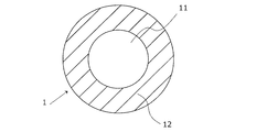
- FIG. 1A is a diagram illustrating an example of an electrophotographic conductive member according to one embodiment of the present invention
- FIG. 1B is a schematic diagram for explaining a first cube and a unit cube according to one embodiment of the present invention.
- FIG. The electrophotographic conductive member 1 according to this aspect includes a matrix containing a first rubber cross-linked product on a conductive substrate (conductive shaft core) 11 as shown in FIG. 1A in cross section. And a conductive layer having a plurality of domains dispersed in the matrix. Note that another layer can be provided on the conductive layer as necessary.
- the electrical resistance of the conductive member is preferably controlled so that the volume resistivity is 10 4 to 10 8 ⁇ cm.
- the conductive substrate can be appropriately selected from those known in the field of electrophotographic conductive members.
- a conductive shaft core body it has a cylindrical shape in which a surface of a carbon steel alloy is nickel-plated with a thickness of about 5 ⁇ m.
- the substrate may be a hollow cylinder.
- a conductive adhesive adheresive
- the conductive layer has a matrix containing a cross-linked product of the first rubber and a plurality of domains dispersed in the matrix.
- ⁇ the average value of the ratio of the cross-sectional area of the conductive particles contained in each domain to the cross-sectional area of each domain appearing in the cross section in the thickness direction of the conductive layer.
- the conductive layer of the conductive member has a uniform semi-conductivity in order to uniformly charge the charged body when used as a charging roller.
- the hardness is preferably low (for example, the elastic modulus of the conductive layer is 1 MPa or more and 100 MPa or less).
- substantially only the domains are made conductive by the conductive particles, and the conductive particles are unevenly distributed in the domains.
- the conductive layer has a matrix containing a crosslinked product of the first rubber.
- the first rubber is not particularly limited as long as it can form a matrix containing the first rubber by blending with the second rubber described later at a predetermined ratio.
- a known rubber composition can be suitably used in the field of electrophotographic conductive members. Examples thereof include natural rubber, a vulcanized product thereof, and synthetic rubber.
- Examples of the synthetic rubber include styrene-butadiene rubber (SBR), acrylonitrile-butadiene rubber (NBR), butadiene rubber (BR), epichlorohydrin rubber, silicone rubber, fluorine rubber, isoprene rubber, chloroprene rubber, and ethylene-propylene rubber. .
- SBR styrene-butadiene rubber
- NBR acrylonitrile-butadiene rubber
- BR butadiene rubber
- epichlorohydrin rubber silicone rubber, fluorine rubber, isoprene rubber, chloroprene rubber, and ethylene-propylene rubber.
- those modified rubbers and copolymers, and further hydrogenated products thereof may be used, and of course, they may be used in combination as appropriate.
- a filler, a softening agent, a processing aid, a tackifier, an anti-tacking agent, a dispersant which are generally used as a rubber compounding agent, as long
- a foaming agent, a conductive additive, roughening particles, and the like can be added.
- a vulcanizing agent, a vulcanization aid, and a vulcanization accelerator can also be added.
- the compounding agent of the rubber blended in the matrix is preferably 0.1 parts by mass or more and 100 parts by mass or less with respect to 100 parts by mass of the first rubber, although it depends on the raw material rubber to be selected.
- the synthetic rubber used is preferably a diene rubber SBR, NBR, BR or a modified rubber thereof.
- NBR and SBR since it has been confirmed that there is little thermal deterioration during kneading, NBR and SBR are particularly preferable as the rubber to be used.
- SBR tends to improve workability and polishability, and may be extremely preferable depending on desired physical properties.
- the matrix contains almost no conductive particles such as carbon black and has an electric resistance higher than that of the domain.
- the matrix containing the cross-linked product of the first rubber is formed mainly from an ion-conductive raw material rubber having a volume resistivity of 1 ⁇ 10 12 ⁇ ⁇ cm or less, conduction between domains having conductive particles is established. Tends to be good, and it is easy to form a three-dimensional good conductive path.
- the necessary conductive particles are required to satisfy the desired electrical resistance as a conductive member. As a result, it becomes difficult to form a three-dimensional good conductive path.
- the electric resistance of the matrix can be measured by thinning the conductive layer of the conductive member and using a minute terminal.
- the thinning means include a sharp razor, a microtome, and a FIB (focused ion beam).
- the film thickness is smaller than the distance between domains measured in advance with a transmission electron microscope (TEM) or scanning electron microscope (SEM). A flake is prepared. Therefore, as a means for thinning, a means capable of producing a very thin sample such as a microtome is preferable.
- the electrical resistance value is measured by first grounding one surface of the thin piece and then measuring the electric resistance value of the matrix and the domain by means of an atomic force microscope (AFM), a scanning probe microscope (SPM), etc. Identify the matrix and domain location. SPM and AFM can also measure hardness distribution. Then, the probe of the matrix is brought into contact, and a ground current when a DC voltage of 50 V is applied is measured and calculated as an electric resistance. At this time, any means capable of measuring the shape of a thin piece, such as SPM or AFM, is preferable because the film thickness of the thin piece can be measured and the electrical resistivity can be measured.
- the measurement of the electrical resistance as described above is performed by cutting out each thin sample from each of the regions obtained by dividing the conductive member into four in the circumferential direction and five in the longitudinal direction. Calculated by arithmetic average of 20 sample results.
- the matrix contains almost no conductive particles such as carbon black and has a higher electrical resistance than the domain.
- the ratio of the volume resistivity between the matrix portion and the domain portion is preferably 5 times or more, more preferably 10 times or more, from the viewpoint of forming a conductive path of the domain.
- the ratio of volume resistivity between the matrix part and the domain part was measured as follows. Similar to the measurement of the electric resistance of the matrix, a thin piece of a conductive layer was prepared, and current measurement was performed in a minute region using an SPM having a current measurement function.
- an SPM scanning area including at least one domain was set. For example, when the domain size is submicron, a scanning area of about several ⁇ m square is set so that a plurality of domains are preferably included.
- One or more subareas corresponding to the matrix are set from current mapping data (data in which current values are stored in each pixel) obtained by scanning while applying a constant voltage, and currents in the plurality of subareas are set.
- the average value of the data is calculated, and the average current value of the matrix portion is Jd. Further, the same analysis is performed for the domain part, and the average current value of the domain part is Jm. From the above data, Jm / Jd was evaluated as the resistance ratio (reciprocal of the current ratio) between the domain part and the matrix part. In the current measurement, the conductive member was divided into four pieces in the circumferential direction and five thin pieces of the conductive layer were cut out from each of the regions divided in the longitudinal direction to obtain the above measured values, and then a total of 20 Calculated by arithmetic mean of sample results.
- the domain constituting the conductive layer has a second rubber.
- the material of the second rubber is not particularly limited as long as it can form a domain containing the second rubber by blending with the first rubber at a predetermined ratio.
- a rubber composition known in the field of electrophotographic conductive members can be suitably used depending on desired physical properties. That is, if it is incompatible with the material of the first rubber, for example, the rubber material shown in the section of “[Matrix] (first rubber material)” can be used as appropriate.
- a diene rubber containing a double bond in the main chain is preferable when carbon black is used as the conductive particles because the compatibility is high depending on the combination.
- diene rubber having a styrene skeleton is also preferable because the compatibility with carbon black tends to increase depending on the combination.
- a rubber material having a functional group that can be expected to interact with conductive particles such as carbon black at the main chain, side chain, or terminal portion of the second rubber it is preferable from the viewpoint of fixing the conductive particles. .
- the material viscosity can be easily adjusted by appropriately blending liquid rubber as the second rubber material.
- the second rubber material forming the domain is a filling generally used as a rubber compounding agent as long as the effects of the present invention are not impaired.
- An agent, a softening agent, a processing aid, a tackifier, an anti-tacking agent, a dispersant, a foaming agent, a conductive aid and the like can also be added.
- a vulcanizing agent, a vulcanization aid, and a vulcanization accelerator can also be added.
- blended with a domain is based also on the raw material rubber to select, 0.1 mass part or more and 50 mass parts or less are preferable with respect to 100 mass parts of 2nd rubber
- a domain is a conductive phase that effectively transports charges in a conductive path in a high speed process.
- the electrical resistivity is preferably low, and specifically, it is preferably 10 ⁇ 1 ⁇ cm to 10 3 ⁇ cm.
- the electrical resistivity of the domain can be set to a desired value by appropriately adjusting the type and amount of the conductive particles.
- the conductive domain includes a second rubber cross-linked product and conductive particles.
- the conductive particles include the following conductive particles.
- Metal fine particles and fibers such as aluminum, palladium, iron, copper and silver; metal oxide fine particles such as titanium oxide, tin oxide and zinc oxide; the surface of the above metal fine particles, fibers and metal oxides
- furnace black the following are mentioned.
- SAF-HS SAF, ISAF-HS, ISAF, ISAF-LS, I-ISAF-HS, HAF-HS, HAF, HAF-LS, T-HS, T-NS, MAF, FEF, GPF, SRF-HS- HM, SRF-LM, ECF, and FEF-HS.
- thermal black examples include FT and MT.
- these conductive particles can be used alone or in combination of two or more.
- the carbon black used is preferably a conductive carbon black having a DBP absorption of 40 ml / 100 g or more and 150 ml / 100 g or less.
- the absorption amount of DBP is a value obtained by indirectly quantifying the structure of primary particles of carbon black. That is, by using carbon black having a structure with a DBP absorption amount within the above range, it has been found that the interaction with the rubber material tends to increase even when the second rubber material with low polarity is used.
- the DBP absorption amount of carbon black can be measured by the method described in JISK6217-4 (2001).
- conductive carbon black since conductive carbon black has a highly developed structure, it can be distinguished from other fillers such as reinforcing carbon black by microscopic observation.
- the blending amount of the conductive particles blended in the domain is 5 parts by mass or more and 150 parts by mass or less with respect to 100 parts by mass of the second rubber. More preferably, it is 20 parts by mass or more and 120 parts by mass or less.
- the percolation in the domain is good, and the conductive particles are well connected to each other. As a result, the conductive path in the domain is “electrically tightly connected” and is stably formed. More preferred is 120 parts by mass or more.
- the content is particularly preferably 60 parts by mass or more and 120 parts by mass or less.
- the blending amount of the conductive particles it becomes possible to act as a conductive domain by setting the blending amount of the conductive particles to 5 parts by mass or more with respect to 100 parts by mass of the second rubber.
- the domain may easily migrate and re-aggregate due to heat or mechanical application. Therefore, as for the compounding quantity of electroconductive particle, 20 mass parts or more are more preferable.
- the effect tends to increase, preferably 60 parts by mass or more, and particularly preferably 80 parts by mass or more. That is, when the content of the conductive particles in the domain is large, the domain becomes hard and migration can be suppressed.
- the blending amount of the conductive particles is larger than 50 parts by mass, a general electrophotographic conductive member is blended in a relatively large amount.
- the conductivity of the domain itself is manifested by electrically connecting the conductive particles in the domain to form a good conductive path.
- the formation of the conductive path correlates with the blending amount and volume occupancy ratio of the conductive particles in the domain, and the higher the ratio, the more stable the percolation. Therefore, the charge transfer efficiency in the conductive path can be increased. Therefore, when the blending amount is increased, the conductive characteristics are enhanced, and a suitable effect is easily exhibited by the present invention.
- the conductive particles exist only in the domain.
- a master batch was prepared in which conductive particles were added only to the second rubber contained in the domain in advance, and then the obtained master batch and the first rubber for forming a matrix were blended. Even in some cases, a phenomenon in which some conductive particles migrate to the matrix may be observed.
- the conductive particles may be present in the matrix as long as they do not contribute to conductivity.
- the abundance of conductive particles that do not contribute to conductivity in the matrix it is preferable that the abundance of conductive particles per unit volume of the matrix is lower than the abundance of conductive particles per unit volume of the domain. 1/5 or less, More preferably, it is 1/10 or less, More preferably, it is 1/100 or less.
- the domain according to the present invention is a conductive phase, and the electrical resistance of the domain may be measured by the same measurement method as the measurement of the electrical resistance of the matrix. Moreover, the measurement of the electrical resistance as described above is performed after obtaining the above measured values by cutting out each thin sample from each of the regions obtained by dividing the conductive member into four in the circumferential direction and five in the longitudinal direction. Calculated by arithmetic average of the results of 20 samples in total.
- one of the more effective means for uniformly distributing the domain throughout the matrix is to make the domain size small and finely dispersed. That is, even if the total volume of the domains in the matrix is the same, the number of domains greatly increases due to miniaturization. In a simple calculation, for example, if there are 100 true spherical domains with a certain radius, when all of the radii are halved, the number is about 800 with the same total volume. For this reason, even if the main total volume is the same, reducing the domain size and increasing the number increases the proportion of the domains present uniformly throughout the conductive layer. As a result, the number of unit cubes satisfying the condition (1) increases, and the effect according to this aspect can be enhanced.
- D [C ⁇ / ⁇ 0 ⁇ ⁇ ] ⁇ f ( ⁇ 0 / ⁇ )
- D Dispersion particle diameter (domain particle diameter)
- ⁇ Interfacial tension
- ⁇ 0 Matrix viscosity
- ⁇ Dispersion phase viscosity (domain viscosity)
- C Constant ⁇ ⁇ : Shear rate
- Methods A The interfacial tension between the first rubber and the second rubber is reduced.
- Methodhod B The viscosity of the first rubber is made closer to the viscosity of the second rubber.
- Methodhod C Increase the shear rate during blending.
- a combination in which the difference in solubility constant between the first rubber and the second rubber (Solubility Parameter: SP value) is selected is to uniformly disperse the conductive domains. Is preferred. Further, as a technique for reducing the interfacial tension, a technique of adding a compatibilizing agent is also suitable. In addition, when SP value difference is too small, it becomes difficult to make the electroconductive particle in a domain unevenly distributed only in a domain, or compatibility becomes too strong and a sea-island structure may not be formed stably.
- Method B Specifically, at the temperature at the time of kneading, selecting the first rubber and the second rubber by a combination of materials having similar viscosities uniformly disperses the conductive domains. It is preferable for this purpose. Here, it is also effective to use liquid rubber or the like as a part of the second rubber of the domain.
- Method C It is effective to simply increase the shear rate during blending and increase the shear time. Although details will be described later, it is particularly effective for the inventors to use “elongation shear” rather than “simple shear” as a shearing mechanism to be applied in addition to an increase in shear rate.
- the size of the domain in the cross section is preferably 0.1 to 2 ⁇ m or less, more preferably 1 ⁇ m or less, and even more preferably 0.5 ⁇ m or less.
- the thickness is 0.4 ⁇ m or less, an extremely high effect in the present invention can be expected.
- the domain size refers to the diameter at the equivalent circle diameter.
- the average domain size indicates an area weighted average domain size.
- the fracture surface at the measurement location of the sample is neatly formed by the following means.
- the fracture surface may be produced by using a freeze fracture method, a cross polisher method, a focused ion beam method (FIB), or the like on the thin piece.
- the FIB method is preferable in consideration of the smoothness of the fracture surface and pretreatment for observation.
- a pretreatment such as a dyeing treatment or a vapor deposition treatment that can suitably obtain the contrast between the domain and the matrix may be performed.
- the thin section subjected to the formation of the fracture surface and the pretreatment can be observed with a laser microscope, a scanning electron microscope (SEM) or a transmission electron microscope (TEM).
- SEM scanning electron microscope
- TEM transmission electron microscope
- a round cut sample is prepared using a sharp razor from a conductive roller.
- the conductive layer can be measured so that three positions (1/4) l, (2/4) l, and (3/4) l can be measured from the end.
- a round slice sample is prepared.
- a cryo-ion milling process is performed on the core layer and the vicinity of the center of the surface of the circular slice sample at 90 ° intervals in the circumferential direction of the roller. Surface out by cryo ion milling.
- the cross section of the conductive layer in each cross section in (1/4) l, (2/4) l, (3/4) l is 90 degrees in the circumferential direction of the roller, and the center part of the surface from the position of the core bar is SEM.
- Product name: Ultraplus, manufactured by Carl Zeiss is observed at a magnification of 5000 times and a pixel count of 4096 ⁇ 3072 (total 12 images, for example, 20 ⁇ m square SEM images can be obtained).
- each of the images obtained by the above observation was binarized and image-analyzed by an image analyzer (product name: LUZEX-AP, manufactured by Nireco), and the obtained domain area S was calculated.
- the circle equivalent diameter is obtained by applying the calculation formula of ⁇ S / ⁇ . In the present disclosure, the equivalent circle diameter is defined as the domain size.
- FIB-SEM is a technique of processing a sample with an FIB (Focused Ion Beam) apparatus and observing an SEM (scanning electron microscope) of an exposed cross section.
- FIB-SEM is a technique of processing a sample with an FIB (Focused Ion Beam) apparatus and observing an SEM (scanning electron microscope) of an exposed cross section.
- SEM scanning electron microscope
- FIG. 2 is a schematic view for explaining the structure of a conductive layer having a matrix containing a first rubber cross-linked product and a plurality of domains dispersed in the matrix.
- a FIB-SEM manufactured by FI Eye Co., Ltd.
- the conductive layer sampling is performed from any nine locations.
- the length in the longitudinal direction is l, (1/4) l, (2/4) from the end.
- the domain structure it is also preferable to perform a pretreatment that suitably obtains the contrast between the domain and the matrix.
- a dyeing process can be suitably used.
- the obtained image was subjected to 3D visualization / analysis software Avizo (registered trademark, manufactured by FEI Corporation), 27 sides included in one sample of a cubic shape having a side of 9 ⁇ m.
- the volume of the domain in the unit cube of 3 ⁇ m is calculated.
- the measurement of the distance between adjacent wall surfaces of the domain can be similarly performed using the 3D visualization / analysis software, and after obtaining the measurement value, it can be calculated by the arithmetic average of the total 27 samples. it can.
- the inventors have determined that the ratio of the cross-sectional area of the conductive particles contained in each of the domains to the cross-sectional area of each of the domains that appears in the conductive layer as a result of intensive studies is 23% or more, more preferably It has been found that there is a tendency to be achieved when it is 28% or more.
- a mixing process using an extension shearing device is also preferable, and a mixing process using a continuous extension shearing device is particularly preferable.
- the average primary particle diameter is preferably 5 nm to 60 nm, particularly preferably 10 nm to 50 nm.
- the average primary particle diameter of the conductive particles is the arithmetic average particle diameter.
- the definition of the average primary particle size is a size of 5 nm or more and 60 nm or less, all of which are a collection of single crystals or crystallites close thereto.
- TEM transmission electron microscope
- SEM scanning electron
- the section of the conductive particles included in each of the domains relative to the cross-sectional area of each of the domains appearing in the cross section in the thickness direction of the conductive layer “ ⁇ / ⁇ ” is calculated when the average value of the ratio of the area is ⁇ and the standard deviation of the ratio is ⁇ . When there is no domain at the center 3 ⁇ m square, another place is randomly observed by SEM.
- the cross-sectional shape of the domain according to the present invention is preferably close to a circle.
- the roundness value shown below is preferably 1 or more and less than 2.
- a roundness of 1 indicates a perfect circle.
- the ratio of the number of domains having a roundness of 1 or more and less than 2 among the domains appearing in the cross section of the conductive layer is 70% or more.
- the effect of this invention increases when this ratio is high, More preferably, it is 80% or more.
- the conductive properties greatly change depending on the shape and anisotropy of the conductive particles (Matsutani et al., Int. J. Mod. Phys.
- the interface area with the matrix is increased, and the following effects can be expected. is there. That is, when the conductive member is disposed in contact with the photosensitive member, the conductive member is mechanically repeatedly compressed near the nip formed between the photosensitive member and the conductive member. At that time, in the case of a perfect circle with extremely high roundness, domain migration based on mechanical energy application is likely to be induced, and as a result, the network structure of the conductive path changes and the electric resistance value of the conductive layer fluctuates. It is assumed that On the other hand, when the value of the roundness of the domain is 1.1 or more, preferably 1.5 or more, it is estimated that this variation is suppressed because the interface area with the matrix increases.
- the domain As a technique for controlling the shape of the domain, particularly a technique for obtaining a domain with good roundness, it is effective to increase the filling amount of the conductive particles in the domain as described above.
- the domain may be heated or mechanically applied depending on the blending process using a general mixing device such as a kneader or roll, or depending on the conditions during processing as a conductive member. May migrate and re-aggregate easily.
- the filling amount of the conductive particles in the domain is high, the domain becomes hard, and as a result, the migration can be suppressed, and deterioration of roundness due to reaggregation can be suppressed.
- by increasing the filling amount it becomes easy to take a share when the second rubber containing the conductive particles is kneaded, and it can be expected that the roundness of the domain is improved.
- the above-described technique for reducing the domain size is also effective. That is, the aspect ratio decreases as the domain size decreases.
- extension shear rather than “simple shear” as a shearing mechanism to be applied.
- mixed processing using a continuous extension shear device tends to give more favorable results.
- the shape of the domain according to the present invention can be quantified using an SEM image obtained by producing and observing a fracture surface in the same manner as the above-described “method for measuring the size of a domain”. That is, for each domain in the SEM image obtained above, binarization and image analysis are performed by an image analysis apparatus (LUZEX-AP, manufactured by Nireco), and roundness is calculated from the average value.
- LUZEX-AP image analysis apparatus
- the roundness is expressed as “JIS B 0621; the difference between the radii of two circles when the distance between the two concentric circles is minimum when the circular shape is sandwiched between two concentric geometric circles.” It is analyzed based on the definition of In addition, when an inorganic filler or rough particles influence image processing in SEM observation of a domain, contrast difference, EDX measurement (SEM / EDX (scanning electron microscope / energy dispersive X-ray spectroscopy)) In addition, it can be calculated by appropriately excluding by using hardness measurement using SPM measurement separately. Here, a domain having an equivalent circle radius of 100 nm or more is used for the calculation.
- the conductive domains having the same electrical resistance are arranged three-dimensionally uniformly and densely. Therefore, it is preferable that the domain size distribution has a uniform domain size and that the domain is fine. Specifically, in the cross section of the conductive layer, it was confirmed that the effect of the present invention was exhibited when the relationship between the domain size and the number satisfied the following relational expressions (1) and (2).
- Relational expression (1) 80 ⁇ 100 ⁇ L2 / L1 ⁇ 100; Relational expression (2) 0 ⁇ 100 ⁇ L3 / L1 ⁇ 20 or less.
- L1 is the total number of the domains appearing in the cross section in the thickness direction of the conductive layer
- L2 is an area measured in the cross section of the domain of 3.0 ⁇ 10 4 nm 2 or more.
- L3 represents the number of domains whose area is less than 2 ⁇ 10 5 nm 2
- L3 represents the number of domains whose area is 1.2 ⁇ 10 5 nm 2 or more.
- the method for producing a conductive member for electrophotography in the present invention is not particularly limited as long as the conductive layer having the configuration of the present invention described above can be formed, and can be formed by appropriately adjusting the following requirements. .
- a conductive member having a matrix containing a cross-linked product of the first rubber and a conductive layer having a domain containing a plurality of cross-linked products of the second rubber dispersed in the matrix is obtained.
- a dispersion device using simple shear which is generally used for mixing and kneading rubber
- elongation shear is also preferably used.
- shear heat generation is increased at the same time, and the material is deteriorated by promoting the breaking of rubber molecular chains, and the domains are re-aggregated. That is, it is important to control the temperature during the machining process at the same time as applying the shearing force.
- a dispersion device using simple shearing cannot provide a uniform share enough to disperse the second rubber compounded with the conductive particles, resulting in local heat generation during processing.
- the domains could not be uniformly and uniformly dispersed.
- a kneader equipped with an extensional shear screw is suitable for uniformly dispersing the domains in the present invention throughout the matrix.
- Elongation shear is a simple shear mechanism in a pressure type kneader, open roll, or twin-screw kneading extruder. It is easy to obtain a domain of any size.
- the present inventors have also confirmed that the domain may not be uniformly finely dispersed in the matrix simply by improving the shearing force in the simple shearing process.
- a twin-screw kneading extruder that can rotate at high speed and can achieve a shear rate that cannot be achieved with conventional pressure kneaders, open rolls or extruders for rubber (product name: KZW15TW-4MG-NH (-6000), manufactured by Technobel).
- KZW15TW-4MG-NH (-6000), manufactured by Technobel
- the shear flow is a flow in which the material is torn by the velocity gradient
- the extension flow in the extension shear is a flow in which the material is stretched in the principal stress direction.
- the electrophotographic conductive member provided with the above-described conductive layer includes (1) a first unvulcanized rubber as a raw material of the first rubber and a second as a raw material of the second rubber. Kneading an unvulcanized rubber mixture containing the unvulcanized rubber and the conductive particles using a kneader equipped with an extensional shear screw to obtain an unvulcanized rubber kneaded product; (2) Forming a layer of the unvulcanized rubber kneaded material on the outer surface of the conductive substrate; and (3) the first unvulcanized rubber and the first in the layer of the unvulcanized rubber kneaded material. And vulcanizing the unvulcanized rubber of 2 to obtain the conductive layer.
- FIG. 3A and FIG. 3B are schematic views for explaining an example of an extensional shear screw used for producing the conductive elastic layer according to this aspect.
- FIG. 3A is a diagram showing a screw provided with an extension shearing mechanism inside the screw
- FIG. 3B is a diagram showing a screw provided with an extension shearing mechanism outside the screw.
- an extension shear device provided with an extension shear screw 31 as shown in FIGS. 3A and 3B.
- FIG. 3A “a“ batch circulation system ” including a screw 3a having an extension shearing mechanism (capillary tube) inside the screw 31”, and “an extension shearing mechanism (capillary tube outside the screw 31) shown in FIG. 3B.
- the hole diameter of the thin tube which gives extension shear is larger than 0.5 mm and is 5.0 mm or less. If it is 5.0 mm or less, the shear share is sufficient, and if it is larger than 0.5 mm, the rubber will not pass through the hole in the narrow tube and processing will not be difficult. Have confirmed.
- the hole diameter of the thin tube is preferably 1.0 to 3.0 mm.
- the treatment time is particularly preferably kneaded in a short time. The shear energy applied to the rubber composition varies depending on the hole diameter of the thin tube.
- the selection of the hole diameter of the narrow tube is one of the important factors in the processing conditions, as well as the material feed rate and the material temperature control during mixing.
- the number of holes in the narrow tube is not particularly limited as long as the desired domain can be uniformly dispersed, and a configuration that can obtain an elongation shear effect in a similar manner without using a narrow tube, such as a double cylindrical configuration, is used. Also good.
- the continuous type is particularly suitable as a processing condition because it has a configuration in which only extension shear is efficiently applied.
- an extension shearing device (micro shear device: manufactured by Imoto Seisakusho or high-speed shearing device: manufactured by Niigata Machine Techno Co., Ltd.) is also preferably used.
- a continuous system apparatus as shown in FIG. 3B, an apparatus in which the screw portion of the batch circulation system apparatus is modified so as to include an extension shearing mechanism inside the screw can be suitably used.
- the bando technical report no. The apparatus described in 18/20147 P2, etc. can also be used suitably.
- the material temperature at the time of dispersion was measured using an infrared thermometer that can be directly measured, and setting it to 170 ° C or less gives good results for uniform dispersion. is doing.
- the temperature at the time of kneading the material is measured with a thermocouple, it tends to be measured lower than the infrared temperature sensor, and good results are obtained even with the same processing at 170 ° C. or lower. It may not be possible.
- it is effective to precisely control the processing process temperature using a mixing apparatus having an extensional shear mechanism equipped with a precise material temperature measurement function (IR sensor).
- a chiller capable of controlling the temperature from room temperature to ⁇ 20 ° C. in order to prevent deterioration of the rubber composition due to shearing heat generation. That is, as described above, when the screw part is equipped with an infrared temperature sensor that accurately monitors the material temperature during mixing, precise mixing condition control is possible, and in particular, the temperature during mixing is set to 170 ° C. It is suitable when setting to the following.
- An electrophotographic image forming apparatus includes the electrophotographic conductive member according to an aspect of the present invention.
- An example of the electrophotographic image forming apparatus is shown in the schematic configuration diagram of FIG.
- the photosensitive member 41 as a member to be charged has a drum shape in which a conductive support 41b having conductivity such as aluminum and a photosensitive layer 41a are stacked on the conductive support 41b. It is rotationally driven with a predetermined peripheral speed in the direction.
- Both ends of the conductive shaft core 11 of the charging roller 1 which is a conductive member for electrophotography according to one aspect of the present invention are pressed against the photoconductor 41 by pressing means (not shown), and the conductive shaft core is The conductive layer 12 to which a direct current (DC) bias is applied by the power source 42 and the rubbing electrode 43a is disposed in contact.
- the charging roller 1 is driven to rotate, so that the photosensitive member 41 is uniformly charged (primarily charged) to a predetermined polarity and potential.
- an electrostatic latent image corresponding to the target image information is formed on the peripheral surface of the photosensitive member that has been exposed to the target image information (laser beam scanning exposure, slit exposure of the original image, etc.) from the exposure unit 44.
- the electrostatic latent image on the photoreceptor is formed into a toner image by attaching toner supplied by the developing member 45.
- the transfer material 47 is conveyed from a paper feed unit (not shown) to the transfer unit between the photoconductor 41 and the transfer member 46 in synchronization with the rotation of the photoconductor 41, and is reverse to the toner image from the back surface of the transfer material.
- the transfer member applied with the polarity is pressed, and the toner images are sequentially transferred onto the transfer material 47.
- the transfer material 47 that has received the transfer of the toner image is separated from the photoreceptor 41 and conveyed to a fixing means (not shown) to fix the toner image and output it as an image formed product.
- a fixing means not shown
- the transfer material 47 is re-conveyed between the photoconductor 41 and the transfer member 46 in order to form another image by the re-conveyance means.
- the peripheral surface of the photoreceptor 41 after the image transfer is subjected to pre-exposure by the pre-exposure device 48, and residual charges on the photoreceptor are removed (static elimination).
- Known means can be used for the pre-exposure device 48.
- an LED chip array, a fuse lamp, a halogen lamp, and a fluorescent lamp can be preferably exemplified.
- the peripheral surface of the photoreceptor 41, which has been neutralized, is cleaned by the cleaning member 49 to remove adhering contaminants such as toner remaining after transfer, and is repeatedly used for image formation.
- the charging roller 1 may be driven by the photosensitive member 41 or may be non-rotated, and is positively driven with a predetermined peripheral speed in the forward direction or the reverse direction in the surface movement direction of the photosensitive member 41. You may make it drive to rotate.
- the electrophotographic image forming apparatus is used as a copying machine, the exposure is reflected or transmitted light from the original, or the original is read as a signal, and a laser beam is scanned based on this signal, or the LED array is It may be driven or a liquid crystal shutter array may be driven.
- Examples of the electrophotographic image forming apparatus of the present invention include a copying machine, a laser beam printer, an LED printer, or an electrophotographic application apparatus such as an electrophotographic plate making system.
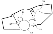
- a process cartridge according to an aspect of the present invention includes the conductive member, and is configured to be detachable from the main body of the electrophotographic image forming apparatus.
- An example of the process cartridge is shown in the block diagram of FIG.
- This process cartridge includes a roller-shaped conductive member according to one embodiment of the present invention as a charging roller 51.
- a drum-shaped electrophotographic photosensitive member (hereinafter also referred to as “electrophotographic photosensitive drum”) 53 is arranged so as to be charged by a charging roller 51.
- the charging roller 51 is pressed against and contacts the electrophotographic photosensitive drum 53.
- a developing roller 55 for supplying a developer for developing the electrostatic latent image formed on the surface of the electrophotographic photosensitive drum 53, and a developer remaining on the peripheral surface of the electrophotographic photosensitive drum 53 are removed.
- a cleaning blade 57 to be removed is provided.
- a developing blade 59 is in contact with the developing roller 55.
- the blade-shaped conductive member according to one embodiment of the present invention can also be used for the developing blade 59.
- a kneaded rubber composition (mixture) in Examples refers to an unvulcanized rubber composition (mixture) to which no crosslinking agent or vulcanization accelerator is added
- B kneaded rubber composition (mixture) refers to a crosslinking agent or It refers to an unvulcanized rubber composition (mixture) to which a vulcanization accelerator is added.
- Example 1 (Production of rubber mixture) 100 parts of ethylene-propylene-diene terpolymer (trade name: EPT4045, manufactured by Mitsui Chemicals) as the raw material of the domain, carbon black (trade name: Ketjen Black EC600JD, manufactured by Ketjen Black International) as the conductive particles ) 3 parts and 40 parts of carbon black (trade name: Toka Black # 7360, manufactured by Tokai Carbon Co., Ltd.), 10 parts of paraffin oil (trade name: PW-380, manufactured by Idemitsu Kosan Co., Ltd.) as softener, stearic acid as processing aid One part was kneaded with a pressure kneader to obtain a master batch 1.
- a round bar having a total length of 252 mm and an outer diameter of 6 mm was prepared by subjecting the surface of free-cutting steel to electroless nickel plating. Next, an adhesive was applied over the entire circumference in a range of 230 mm in length excluding 11 mm at both ends of the round bar.
- the adhesive used was a conductive hot melt type.
- a roll coater was used for coating.
- a round bar coated with this adhesive was used as a conductive shaft core (core metal).
- a crosshead extruder having a conductive shaft core supply mechanism and an unvulcanized rubber roller discharge mechanism was prepared.
- a die having an inner diameter of 12.5 mm was attached to the cross head, the extruder and the cross head were adjusted to 80 ° C., and the conveying speed of the conductive shaft core was adjusted to 60 mm / sec.
- the B kneaded rubber composition 1 is supplied from a kneading extruder to form a rubber layer of the B kneaded rubber composition 1 on the outer peripheral surface of the conductive shaft core in the crosshead.
- a vulcanized rubber roller was obtained.
- an unvulcanized rubber roller was put into a hot air vulcanizing furnace at 170 ° C.
- a crown-shaped conductive roller having a diameter of 8.4 mm and a center diameter of 8.5 mm at positions of 90 mm from the central portion to both end portions was obtained.
- the roller had an electric resistance value of 5.0 ⁇ 10 5 ⁇ ⁇ cm.
- the measurement method used was “measurement of partial resistance value of conductive roller” described later.
- the conductive elastic layer of the conductive roller according to each embodiment has a plurality of domains in the first rubber matrix, each domain satisfies the configuration including conductive particles, That the average value ⁇ of the ratio of the cross-sectional area of the conductive particles included in each domain relative to the cross-sectional area of each domain is 20% or more and 40% or less is shown in the above-described domain measurement method and the like. The method was confirmed.
- the product name: Leica EM UC7 manufactured by Leica Co., Ltd., the product name Leica EMTIC3X manufactured by Leica Co., Ltd., and the product name: Ultraplus, manufactured by Carl Zeiss are used as the microtome. It was.
- the effect according to this aspect can be enhanced by increasing the number of unit cubes satisfying the condition (1).
- the level of uniform dispersion of the domain was evaluated based on the following criteria based on the above measurement results.
- the conductive layer exhibits homogeneous and stable electric characteristics in the order of rank I> II> III> IV> V.
- Rank I Uniform dispersibility is very good. (The number of unit cubes satisfying the condition (1) is 25 or more in at least 8 samples)
- Rank II Uniform dispersibility is fairly good. (The number of unit cubes satisfying the condition (1) is less than 25 in at least 2 samples and 22 or more in at least 8 samples)
- Rank III Uniform dispersibility is good. (The number of unit cubes satisfying the condition (1) is less than 22 in at least 2 samples and 20 or more in at least 8 samples)
- Rank IV Uniform dispersibility is not recognized. (The number of unit cubes satisfying the condition (1) is less than 20 in at least 2 samples and 12 or more in at least 8 samples)
- Rank V Uniform dispersibility is extremely poor. (The number of unit cubes satisfying the condition (1) is less than 12 in at least two samples)
- ⁇ (Evaluation of variation of conductive particles in each domain in the conductive layer) It was verified using the measurement method described above that the conductive domain was a domain with uniform electrical resistance. “The average value of the ratio of the cross-sectional area of the conductive particles included in each domain to the cross-sectional area of each domain appearing in the cross section in the thickness direction of the conductive layer is ⁇ , and the standard deviation of the ratio is ⁇ . In this case, the smaller the “ ⁇ / ⁇ ” is, the higher the effect according to this aspect is, and the level of variation of the conductive particles in each domain was evaluated based on the above measurement results based on the following criteria. In the order of rank i>ii> iii, the domains have the same electric resistance.
- Rank i The variation of the conductive particles is extremely small. (0 ⁇ ⁇ / ⁇ ⁇ 0.25) Rank ii: Small variation in conductive particles. (0.25 ⁇ / ⁇ ⁇ 0.4) Rank iii: Large variation in conductive particles. ( ⁇ / ⁇ ⁇ 0.4)
- the domain shape is preferably close to a circle, and was evaluated based on the roundness based on the measurement method described above.
- the roundness level was evaluated based on the following criteria. In addition, it has shown that it is near circular in order of rank a>b>c> d.
- Rank a The roundness is recognized very well. (Average roundness is 1 or more and less than 1.90) Rank b: Good roundness is recognized. (Average roundness is 1.90 or more and less than 2.0) Rank c: The roundness is poor. (Average roundness is 2.10 or more and less than 22.60) Rank d: The roundness is extremely poor. (The average value of roundness is 2.60 or more)
- the size distribution of the domain it is preferable that the domain size is uniform and that the domain is fine. Based on the above-described measurement method, the domain size distribution was evaluated based on the particle size distribution uniformity based on the ratio of the large domain to the small domain. .
- the SEM image is calculated from 12 or more evaluations.
- the level of particle size distribution uniformity was evaluated based on the following criteria. In addition, in order of rank 1>2>3> 4, the particle size distribution uniformity is high. Rank 1: The particle size distribution uniformity is extremely high. (95 ⁇ 100 ⁇ L2 / L1 ⁇ 100 and 0 ⁇ 100 ⁇ L3 / L1 ⁇ 5) Rank 2: Uniformity of particle size distribution is high. (80 ⁇ 100 ⁇ L2 / L1 ⁇ 95 and / or 15 ⁇ 100 ⁇ L3 / L1 ⁇ 20) Rank 3: The particle size distribution uniformity is poor.
- the electric resistance of the conductive roller in the partial area was measured in a state where a metal electrode was pressed against the conductive roller and a DC voltage was applied to the conductive shaft core of the conductive roller using an external power source.
- the value of the current flowing through the partial region was calculated based on the voltage across the reference resistor connected in series with the metal electrode and the electrical resistance value of this voltage and the reference resistor.
- the resistance value of the conductive roller is measured by applying a constant DC voltage between the conductive shaft core of the conductive roller and the metal electrode using an electrometer or the like that can measure a minute current. The current value may be measured with.
- the current value of the conductive roller was measured for 10 seconds in a state where a fixed voltage of DC 20 V was applied between the conductive shaft core and the metal electrode in an environment of a temperature of 23 ° C. and a relative humidity of 50%. I went later.
- the volume resistivity ( ⁇ ⁇ cm) of the partial region was calculated from the measured current value, the area where the conductive roller and the metal electrode were in contact, the thickness of the conductive layer of the conductive roller, and the voltage applied to the conductive layer. .
- ⁇ Measurement of partial resistance of conductive roller (method using rotating electrode) The value of current flowing in a partial region of the conductive roller was measured using an electrical resistance measuring device described in detail below.
- a cylindrical metallic rotating electrode having a diameter of 30 mm and a width of 20 mm is pressed at a predetermined pressure at an arbitrary position of the conductive roller, the conductive roller is rotated, and the rotation is performed in accordance with the rotational movement of the conductive roller.
- the electrode is driven to rotate. Further, the voltage across the reference resistor connected in series with the rotating electrode is measured in a state where a DC voltage is applied to the conductive shaft core of the conductive roller using an external power source.
- the value of current flowing through the region defined by the contact surface between the rotating electrode and the conductive roller in the conductive layer of the conductive roller can be obtained.
- the area of the contact surface is about 0.05 to 0.2 cm 2 depending on the hardness of the conductive layer.
- the rotational speed of the conductive roller was set to 30 rpm, the data sampling frequency was set to 20 Hz, and the electric resistance value of the reference resistance was set to 1 k ⁇ .
- the applied voltage depends on the electrical resistivity of the conductive layer, a fixed voltage was set between 10 and 200 V so that the current value was about 0.1 mA. Under the above conditions, it is possible to measure about 12 areas per circumference on the roller surface in the circumferential direction every about 0.6 mm.
- the rotating electrodes were sequentially moved in the longitudinal direction of the roller, and similarly, the current was measured in a total of about 140 regions while rotating the conductive roller. Moreover, the volume resistivity ( ⁇ ⁇ cm) of the partial region is calculated from the measured current value, the contact area between the conductive roller and the rotating electrode, the thickness of the conductive layer of the conductive roller, and the voltage applied to the conductive layer. did. Variations in the volume resistivity of a conductive roller in the average of the volume resistivity of the partial regions of the measurement mu R, dispersed and sigma R, was evaluated by ⁇ R / ⁇ R.
- ⁇ R / ⁇ R The level of ⁇ R / ⁇ R of electrical resistance was evaluated based on the following criteria based on the above results. It shows that the conductive layer exhibits homogeneous and stable electrical characteristics in the order of rank A>B>C> D.
- Rank A ⁇ R / ⁇ R is extremely small.
- Rank B ⁇ R / ⁇ R is quite small.
- Rank C ⁇ R / ⁇ R is small.
- Rank D ⁇ R / ⁇ R is large. (0.5 ⁇ ⁇ R / ⁇ R )
- an energization deterioration test of the conductive roller was performed in an environment of a temperature of 23 ° C. and a relative humidity of 50%.
- a constant voltage set at 50 V DC was applied between the conductive shaft core and the metal drum for 10 minutes.
- the rotation speed of the metal drum was set at 30 rpm, and the electric resistance value of the reference resistance was set between 100 ⁇ and 1 k ⁇ .
- the data sampling frequency was set to 20 Hz, and the average value of the measured values for 10 seconds was defined as the current value flowing through the conductive roller.
- the initial current value I0 and the current value I1 at the end of the energization test were calculated, and the current maintenance ratio (%) was calculated as the ratio of I1 to I0.
- Rank A The current maintenance rate is extremely high. (Maintenance rate is 85% or more)
- Rank B The current maintenance rate is slightly recognized. (Maintenance rate is 70% or more and less than 85%)
- Rank C A current maintenance ratio is recognized. (Maintenance rate is 60% or more and less than 70%)
- Rank D No current maintenance rate is recognized. (Maintenance rate is less than 60%)
- Image evaluation of conductive roller Image evaluation was performed in a high-speed process of a conductive member.
- an electrophotographic laser printer (trade name: Laserjet M608dn, manufactured by HP) was prepared as an electrophotographic apparatus.
- the conductive member, the electrophotographic apparatus, and the process cartridge were left in an environment of 23 ° C. and 50% RH for 48 hours for the purpose of adjusting the measurement environment.
- the laser printer was modified so that the number of output sheets per unit time was 75 sheets / minute with A4 size paper, which is larger than the original output number. At that time, the output speed of the recording medium was 370 mm / second, and the image resolution was 1,200 dpi.
- the produced conductive roller was mounted on an electrophotographic process cartridge as a charging roller. Under the same environment as described above, a voltage of ⁇ 900 V was applied to the conductive member by an external power source (manufactured by Trek615 Trek Japan) to output a halftone image. That is, one electrophotographic image in which a halftone image (an image in which a line with a width of 1 dot is drawn at intervals of 2 dots in the direction perpendicular to the rotation direction of the electrophotographic photosensitive member) is formed on A4 size paper was output. This image is referred to as a “first image”.
- Rank A A uniform image having no graininess from the beginning, and no deterioration in graininess is observed even after durability.
- Rank B A uniform image without graininess in the initial stage, and the deterioration of graininess is slightly recognized after durability.
- Rank C An image having graininess (deterioration in graininess) is recognized from the beginning.
- Rank D An image with graininess (deterioration in graininess) is noticeable from the beginning.
- Example 2 100 parts of SBR (trade name: Toughden 2003, manufactured by Asahi Kasei Co., Ltd.) as the raw material of the domain, 3 parts of carbon black (trade name: Ketjen Black EC600JD, manufactured by Ketjen Black International) as the conductive particles, and carbon black (trade name) : Toka Black # 5500, manufactured by Tokai Carbon Co., Ltd.) 40 parts and 1 part of stearic acid as a processing aid were kneaded with a pressure kneader to obtain a master batch 2.
- SBR trade name: Toughden 2003, manufactured by Asahi Kasei Co., Ltd.
- carbon black trade name: Ketjen Black EC600JD, manufactured by Ketjen Black International
- carbon black trade name: Toka Black # 5500, manufactured by Tokai Carbon Co., Ltd.
- NBR trade name: N230SV, manufactured by JSR
- 10 parts of calcium carbonate trade name: Nanox # 30, manufactured by Maruo Calcium Co., Ltd.
- a pressure kneader trade name: TD6-15MDX: manufactured by Toshin Co., Ltd.
- the rubber composition 2 for a matrix was obtained by mixing under the conditions of a filling rate of 70%, a blade rotation speed of 30 rpm, and a mixing time of 16 minutes.
- Example 3 90 parts of SBR (trade name: Toughden 2003, manufactured by Asahi Kasei Co., Ltd.) and 10 parts of liquid SBR (trade name: LIR-310, manufactured by Kuraray Co., Ltd.), carbon black (trade name: Talker Black) as conductive particles 60 parts of # 5500 (manufactured by Tokai Carbon Co., Ltd.) and 1 part of stearic acid as a processing aid were kneaded with a pressure kneader to obtain a master batch 3.
- 20 parts of the masterbatch 3 prepared above and 72 parts of the rubber composition 2 for matrix prepared in Example 2 were mixed for 13 minutes using a pressure kneader, and the unvulcanized rubber mixture 3 was mixed.
- the master batch was divided into five equal parts and mixed stepwise. Except for these, a conductive roller was produced in the same manner as in Example 2, and each evaluation was performed. The roller had an electric resistance of 8.5 ⁇ 10 5 ⁇ ⁇ cm.
- Example 4 A corresponding rubber mixture was prepared in the same manner as in Example 1. That is, 120 parts of epichlorohydrin-ethylene oxide-allyl glycidyl ether terpolymer (trade name: Epichromer CG, manufactured by Osaka Soda Co., Ltd.), 1 part of stearic acid as a processing aid, 40 masterbatches 1 prepared in Example 1 were used. Are mixed with an open roll to obtain an unvulcanized rubber mixture 4. Here, the master batch was divided into five equal parts and mixed stepwise. Next, using the processing machine (product name: NHSS8-28, manufactured by Niigata Machine Techno Co., Ltd.) having a screw having an extension shearing mechanism inside the screw as an extension shear molding processing machine shown in FIG.
- the processing machine product name: NHSS8-28, manufactured by Niigata Machine Techno Co., Ltd.
- Sulfur rubber (A-kneaded rubber composition) was kneaded.
- the hole of the thin tube of the screw equipped in the processing machine is set to 2.0 mm
- the plasticizing part temperature is 100 ° C.
- the kneading part temperature is 150 ° C.
- the screw rotation speed is set to 750 rpm. Kneaded.
- the rubber composition was stretched and sheared by discharging from the kneading section. By repeating this, an amount sufficient for producing the conductive roller was produced.
- the temperature of the kneading part was controlled so as not to exceed 170 ° C. by using a cooling mechanism.
- vulcanizing agent / sulfur (trade name: SULFAX PMC, manufactured by Tsurumi Chemical Co., Ltd.), vulcanization accelerator (trade name: Perkacit TBzTD, 6.8 parts of Performance Additives) were added. Subsequently, it knead
- Example 5 100 parts of SBR (trade name: Toughden 2003, manufactured by Asahi Kasei Co., Ltd.) as the raw material of the domain, 70 parts of carbon black (trade name: Toka Black # 5500, manufactured by Tokai Carbon Co., Ltd.) as the conductive particles, stearic acid 1 as the processing aid The parts were kneaded with a pressure kneader to obtain a master batch 5. Next, 22 parts of the master batch 5 and 68 parts of the rubber composition 2 for the matrix produced in Example 2 were mixed for 20 minutes using a pressure kneader to obtain an unvulcanized rubber composition 5. . Except for these, a conductive roller was produced in the same manner as in Example 2, and each evaluation was performed. The roller had an electric resistance of 4.0 ⁇ 10 5 ⁇ ⁇ cm.
- Example 6 100 parts of terminal-modified SBR (trade name: Toughden E581, manufactured by Asahi Kasei), 80 parts of carbon black (trade name: Toka Black # 5500, manufactured by Tokai Carbon Co., Ltd.) as conductive particles, and stearin as processing aid 1 part of the acid was kneaded with a pressure kneader to obtain a master batch 6. Next, 25 parts of the master batch 6 prepared above and 70 parts of the matrix rubber composition 2 prepared in Example 2 were mixed for 16 minutes using a pressure kneader, and the unvulcanized rubber composition was mixed. 6 was obtained. Here, the master batch was divided into 5 equal parts and mixed with the rubber composition 2 for the matrix stepwise. The electric resistance of the roller was 3.5 ⁇ 10 5 ⁇ ⁇ cm.
- Example 7 100 parts of SBR (trade name: Toughden 2003, manufactured by Asahi Kasei Co., Ltd.) as the raw material of the domain, 85 parts of carbon black (trade name: Toka Black # 7360, manufactured by Tokai Carbon Co., Ltd.) as the conductive particles, stearic acid 1 as the processing aid The parts were kneaded with a pressure kneader to obtain a master batch 7. Next, 30 parts of the master batch 7 and 65 parts of the rubber composition 2 for the matrix produced in Example 2 were mixed with an open roll to obtain a corresponding unvulcanized rubber mixture 7.
- Example 4 the unvulcanized rubber (A kneaded rubber composition) was kneaded using an extension shear molding machine having a screw provided with an extension shearing mechanism inside the screw.
- the processing was performed under the same conditions except that the screw rotation speed was set to 800 rpm.
- a conductive roller was produced in the same manner as in Example 4, and each evaluation was performed.
- the roller had an electric resistance of 8.0 ⁇ 10 5 ⁇ ⁇ cm.
- Example 8 As raw materials for the domain, emulsion-polymerized styrene-butadiene rubber, 100 parts of E-SBR (trade name: JSR0202, manufactured by JSR) and 10 parts of liquid SBR (trade name: LIR-310, manufactured by Kuraray), carbon as conductive particles 100 parts of black (trade name: Toka Black # 5500, manufactured by Tokai Carbon Co., Ltd.) and 1 part of stearic acid as a processing aid were kneaded with a pressure kneader to obtain a master batch 8. Next, 34 parts of the master batch 8 and 70 parts of the rubber composition 2 for the matrix produced in Example 2 were mixed with an open roll to obtain an unvulcanized rubber mixture 8.
- E-SBR trade name: JSR0202, manufactured by JSR
- liquid SBR trade name: LIR-310, manufactured by Kuraray
- carbon as conductive particles 100 parts of black (trade name: Toka Black # 5500, manufactured by Tokai Carbon Co., Ltd.) and
- an extension shear forming machine As a continuous processing machine having a screw having an extension shearing mechanism on the outside of the screw, an extension shear molding having a screw having an extension shearing mechanism inside the screw used in Example 7.
- a processing machine product name: NHSS8-28, manufactured by Niigata Machine Techno
- continuous extension shear molding is possible by adopting the apparatus configuration shown in FIG. 3B in which the screw tip is modified so that the hole 32 of the thin tube is held outside rather than inside the screw.
- the unvulcanized rubber (A kneaded rubber composition) was kneaded using a continuous extension shear molding machine having a screw provided with the extension shearing application mechanism.
- the processing was performed under the same conditions except that the screw rotation speed was set to 600 rpm. Except for these, a conductive roller was produced in the same manner as in Example 4, and each evaluation was performed.
- the roller had an electric resistance of 8.0 ⁇ 10 5 ⁇ cm.
- Example 9 100 parts of NBR (trade name: N230SV, manufactured by JSR) as a raw material of the domain, 60 parts of carbon black (trade name: Toka Black # 7360, manufactured by Tokai Carbon Co.) as conductive particles, carbon black (trade name: Ketjen) Black EC600JD (manufactured by Ketjen Black International Co., Ltd.) 10 parts and 1 part of stearic acid as a processing aid were kneaded with a pressure kneader to obtain a master batch 9.
- NBR trade name: N230SV, manufactured by JSR
- carbon black trade name: Toka Black # 7360, manufactured by Tokai Carbon Co.
- carbon black trade name: Ketjen
- EC600JD manufactured by Ketjen Black International Co., Ltd.
- a rubber mixture was prepared based on Patent Document 1. That is, 100 parts of an ethylene-propylene-diene terpolymer (trade name: EPT4045, manufactured by Mitsui Chemicals) as a domain material, and carbon black (trade name: Ketjen Black EC600JD, manufactured by Ketjen Black International) as conductive particles. 10 parts, 30 parts of paraffin oil (trade name: PW-380, manufactured by Idemitsu Kosan Co., Ltd.) as a softening agent, and 1 part of stearic acid as a processing aid were kneaded with a pressure kneader to obtain a master batch.
- EPT4045 ethylene-propylene-diene terpolymer
- carbon black trade name: Ketjen Black EC600JD, manufactured by Ketjen Black International
- epichlorohydrin-ethylene oxide-allyl glycidyl ether terpolymer (trade name: Epichromer CG, manufactured by Osaka Soda Co., Ltd.) 75 parts as a matrix material, stearic acid 1 part as a processing aid, and masterbatch 10 35.25.
- Example 2 In Example 2, in master batch 2, the amount of ketjen black was changed to 3.5 parts and the amount of carbon black was changed to 35 parts to produce a corresponding unvulcanized rubber composition 2A, and unvulcanized A conductive roller was produced and evaluated in the same manner as in Example 1 except that the kneading time of the pressure kneader was 5 minutes when producing the rubber composition 2A.
- the roller had an electric resistance of 4.1 ⁇ 10 6 ⁇ cm.
- the mixture (A kneaded rubber composition) was kneaded.
- 2,5-dimethyl-2,5-di (t-butylperoxy) hexyne (trade name: Perhexa 25B-40, Nippon Oil & Fats as a vulcanizing agent)
- 2.5 parts of triallyl isocyanurate (trade name: TAIC-M60, manufactured by Nippon Kasei Co., Ltd.) is mixed with an open roll, and an unvulcanized rubber mixture (B kneaded rubber)
- a conductive roller was prepared and evaluated in the same manner as in Comparative Example 1 except that the composition 3A) was obtained.
- the roller had an electric resistance of 1.2 ⁇ 10 7 ⁇ cm.
- Example 4 In Example 2, in master batch 2, the amount of ketjen black was changed to 3.5 parts and the amount of carbon black was changed to 35 parts to produce a corresponding unvulcanized rubber composition 4A, and unvulcanized When the rubber composition 4A was prepared, the kneading time of the pressure kneader was 40 minutes (the material temperature at the time of kneading (measured using an infrared thermometer) was increased to 183 degrees) In the same manner as in Example 2, a conductive roller was prepared and evaluated. The roller had an electric resistance of 2.2 ⁇ 10 6 ⁇ cm.
- Example 5 In Example 3, 25 parts of the master batch 3 prepared above and 70 parts of the matrix rubber composition 2 prepared in Example 2 were mixed using two rolls. Thereafter, the same procedure as in Example 3 was performed except that the corresponding unvulcanized rubber mixture 5A (A kneaded rubber composition) was kneaded using the biaxial kneading apparatus shown in Comparative Example 3 at a rotational speed of 1000 rpm. A conductive roller was prepared and evaluated. The roller had an electric resistance of 9.6 ⁇ 10 6 ⁇ cm.
- Example 6 In addition to mixing in Example 8 using a pressure kneader instead of an extension shear molding machine for 10 minutes, 20 parts of master batch 8 and rubber composition 2 for matrix prepared in Example 2 were used. A conductive roller was prepared and evaluated in the same manner as in Example 8 except that 70 parts were used. The roller had an electric resistance of 9.0 ⁇ 10 5 ⁇ cm.
- Example 7 The mixing in Example 8 was carried out by using two rolls instead of the elongation shear molding machine (here, the master batch was divided into 10 equal parts and mixed stepwise), and the master batch 8 was changed to 14.
- a conductive roller was prepared and evaluated in the same manner as in Example 8 except that 6 parts of the rubber composition 2 for a matrix prepared in Example 2 was used in an amount of 70 parts.
- the roller had an electric resistance of 4.9 ⁇ 10 6 ⁇ cm.
- Table 1 shows evaluation of uniform dispersion of domains, evaluation of variation of conductive particles in each domain, evaluation of domain shape, and evaluation of particle size distribution of domains in Examples 1 to 9 and Comparative Examples 1 to 7. , Used mixing device, average domain size in cross section, conductive roller evaluation: electrical resistance ⁇ / ⁇ , and conductive roller evaluation: current maintenance rate and evaluation result of image quality rank.
- Example 10 Provided below, the examination result applied to the transfer roller as a conductive roller is shown.
- Example 10> -Production of conductive roller A round bar having a total length of 240 mm and an outer diameter of 5 mm prepared by electroless nickel plating on the surface of free-cutting steel was prepared. Next, an adhesive was applied over the entire circumference in a range of 210 mm in length excluding 15 mm at both ends of the round bar. The adhesive used was a conductive hot melt type. A roll coater was used for coating. A round bar coated with this adhesive was used as a conductive shaft core (core metal).
- a crosshead extruder having a conductive shaft core supply mechanism and an unvulcanized rubber roller discharge mechanism is prepared, and a die having an inner diameter of 13.5 mm is attached to the crosshead. Furthermore, the conveyance speed of the conductive shaft core was adjusted to 60 mm / sec. Under this condition, the unvulcanized rubber mixture 2 obtained in Example 2 is supplied from a kneading extruder to form a rubber layer of the unvulcanized rubber mixture on the outer peripheral surface of the conductive shaft core in the cross head. An unvulcanized rubber roller was obtained. Next, an unvulcanized rubber roller was put into a hot air vulcanizing furnace at 170 ° C. and heated for 60 minutes to obtain a vulcanized rubber roller.
- the obtained conductive roller was evaluated in the same manner as in Example 1 except for the image quality evaluation.
- the following image quality evaluation 1 of the conductive roller and image quality evaluation 2 of the conductive roller are added instead.
- ⁇ Image evaluation of conductive roller 1 The above conductive roller was used as a transfer roller and mounted on an electrophotographic process cartridge (trade name: HP 30A Black Original LaserJet Toner, HP). This process cartridge was mounted on an electrophotographic image forming apparatus (trade name: HP LaserJet Pro M203dw, manufactured by HP) capable of outputting A4 size paper to form an electrophotographic image.
- HP LaserJet Pro M203dw an electrophotographic image forming apparatus
- Rank A No vertical line crushing or occurrence of a sticky image is observed.
- Rank B Vertical lines are crushed and the occurrence of potty images is slightly recognized.
- Rank C Vertical lines are crushed and the occurrence of potty images is observed.
- Rank D Vertical lines are crushed and the occurrence of potty images is noticeable.
- the electroconductive process cartridge (trade name: HP 30A Black Original LaserJet Toner, manufactured by HP) was mounted as a transfer roller using the conductive roller after the above-described energization deterioration test was performed.
- This process cartridge was mounted on an electrophotographic image forming apparatus (trade name: HP LaserJet Pro M203dw, manufactured by HP) capable of outputting A4 size paper to form an electrophotographic image.
- HP LaserJet Pro M203dw manufactured by HP
- the output of the electrophotographic image was performed in an environment with a temperature of 15 ° C. and a relative humidity of 10%. The image was visually observed, and the presence or absence of a spot-like image that may occur due to an increase in the electrical resistance value of the transfer roller and the degree thereof were evaluated according to the following criteria.
- Rank A Generation of a spot-like image is not recognized.
- Rank B The occurrence of a spot-like image is slightly recognized.
- Rank C Generation of a spot-like image is recognized.
- Rank D The occurrence of a spot-like image is noticeable.
- Example 11 the unvulcanized rubber mixture 4 obtained in Example 4 was used as the unvulcanized rubber mixture. Other than that was carried out similarly to Example 10, and produced the electroconductive roller and performed each evaluation.
- the roller had an electric resistance of 3.2 ⁇ 10 6 ⁇ cm.
- Example 12 the unvulcanized rubber mixture 8 obtained in Example 8 was used as the unvulcanized rubber mixture. Other than that was carried out similarly to Example 10, and produced the electroconductive roller and performed each evaluation. The roller had an electric resistance of 2.4 ⁇ 10 6 ⁇ cm.
- Example 10 the unvulcanized rubber mixture 1A obtained in Comparative Example 1 was used as the unvulcanized rubber mixture. Other than that was carried out similarly to Example 10, and produced the electroconductive roller and performed each evaluation. The roller had an electric resistance of 2.1 ⁇ 10 6 ⁇ cm.
- Example 13 -Production of conductive blade B kneaded rubber mixture 2 (unvulcanized rubber mixture) obtained in Example 2 was used.
- the B-kneaded rubber mixture 2 is treated at 160 ° C. for 10 minutes while pressing it with a pressure press machine onto a mold having a width of 250 mm, a length of 150 mm, and a thickness of 0.7 mm, thereby obtaining a corresponding thickness of 0.
- a 7 mm rubber sheet 1 was obtained.
- the rubber sheet 1 is cut to a width of 216 mm and a length of 12 mm and bonded to a sheet metal (substantially the same shape as a sheet metal used for a developing blade of an electrophotographic process cartridge to be described later) processed in advance to be attached to a predetermined cartridge.
- the conductive rubber blade 1 was obtained by bonding using an agent. At this time, the conductive blade was bonded so that the portion of 12 mm in length overlapping the sheet metal was 4.5 mm, and the remaining 7.5 mm was protruded from the sheet metal.
- the adhesive used was a conductive hot melt type.
- the electric resistance of the conductive blade was 4.2 ⁇ 10 5 ⁇ cm.
- ⁇ Evaluation measurement location of uniform dispersibility of domains in conductive layer Measured at 9 locations near each center in a section of width 24 mm, length 12 mm and thickness 0.7 mm obtained by dividing the width of the rubber sheet into 9 parts.
- ⁇ Evaluation measurement location of variation of conductive particles in each domain in conductive layer Measured at 12 locations around the center in a section of 18 mm wide, 12 mm thick, and 0.7 mm thick divided into 12 rubber sheet widths.
- ⁇ Evaluation of the shape of the domain in the conductive layer of the conductive blade to the roundness measurement location The rubber sheet width is divided into 12 sections, each having 12 locations near the center in a section of 18 mm width, 12 mm thickness, and 0.7 mm thickness. Measurement. -Evaluation measurement location of domain particle size distribution in conductive layer: Measured at 12 locations around the center in a section of 18 mm wide, 12 mm thick, and 0.7 mm wide divided into 12 rubber sheet widths.
- the electric resistance value of the reference resistor was set to 1 k ⁇ . Further, the length of the conductive blade was divided into 20 sections, and a total of 20 areas were measured. For the volume resistivity of the conductive blade, the volume resistivity ( ⁇ ⁇ cm) of the partial region was calculated from the area of the conductive blade rubber part and the metal electrode, the thickness of the rubber part of the conductive blade, and the applied voltage. . Variations in the volume resistivity of a conductive inside blades, the average of the volume resistivity of the partial region of the measurement mu R, dispersed and sigma R, was evaluated by ⁇ R / ⁇ R.
- ⁇ R / ⁇ R The level of ⁇ R / ⁇ R of electrical resistance was evaluated based on the following criteria based on the above results. It shows that the conductive layer exhibits homogeneous and stable electrical characteristics in the order of rank A>B>C> D.
- Rank A ⁇ R / ⁇ R is extremely small. ( ⁇ R / ⁇ R ⁇ 0.25)
- Rank B ⁇ R / ⁇ R is quite small. (0.25 ⁇ R / ⁇ R ⁇ 0.32)
- Rank C ⁇ R / ⁇ R is small. (0.32 ⁇ R / ⁇ R ⁇ 0.4)
- Rank D ⁇ R / ⁇ R is large. (0.4 ⁇ ⁇ R / ⁇ R )
- the level of the current maintenance rate was evaluated based on the following criteria based on the above results. Of course, it is shown that the conductive layers exhibit homogeneous and stable electrical characteristics in the order of rank A>B>C> D.
- Rank A The current maintenance rate is extremely high. (Maintenance rate is 85% or more)
- Rank B The current maintenance rate is slightly recognized. (Maintenance rate is 70% or more and less than 85%)
- Rank C A current maintenance ratio is recognized. (Maintenance rate is 60% or more and less than 70%)
- Rank D The current maintenance rate is noticeable. (Maintenance rate is less than 60%)
- E character image an image in which the letter “E” of the alphabet with a size of 14 points is printed so that the coverage is 1% with respect to the area of the A4 size paper (hereinafter also referred to as “E character image”).
- E character image an image in which the letter “E” of the alphabet with a size of 14 points is printed so that the coverage is 1% with respect to the area of the A4 size paper.
- the triboelectric charge distribution was measured for the toner carried on the narrow portion of the portion of the developing sleeve sandwiched between the developing blade and the photoreceptor contact position.
- the triboelectric charge amount distribution was measured using an E-spar Analyzer Model EST-III (manufactured by Hosokawa Micron). The number of measured particles was about 3000, and the standard deviation ⁇ of the measured value was used as the triboelectric charge amount distribution of the toner.
- the evaluation criteria for evaluating the triboelectric charge amount distribution of the toner are as follows. Rank A: The triboelectric charge amount distribution is very good. ( ⁇ ⁇ 3.0) Rank B: The triboelectric charge amount distribution is quite good. (3.0 ⁇ ⁇ ⁇ 4.0) Rank C: The triboelectric charge amount distribution is good. (4.0 ⁇ ⁇ ⁇ 5.0) Rank D: The triboelectric charge distribution is bad. ( ⁇ > 5.0)
- the above-mentioned conductive blade was used as a developing blade and attached to an electrophotographic process cartridge (trade name: 37X black toner cartridge, manufactured by HP).
- This process cartridge was mounted on an electrophotographic image forming apparatus (trade name: HP LaserJet Enterprise M608dn, manufactured by HP) capable of outputting A4 size paper to form an electrophotographic image.
- HP LaserJet Enterprise M608dn manufactured by HP
- a halftone image an image in which a line with a width of 1 dot is drawn at intervals of 2 dots in the direction perpendicular to the rotation direction of the electrophotographic photosensitive member
- One formed electrophotographic image was output.
- the output of the electrophotographic image was performed in an environment with a temperature of 15 ° C. and a relative humidity of 10%.
- the central part of the image was visually observed, and the presence or absence of density unevenness that might be caused by the unevenness of the conductive point of the conductive blade and the degree thereof were evaluated according to the following criteria.
- Rank A Generation of density unevenness is not recognized.
- Rank B The occurrence of density unevenness is slightly recognized.
- Rank C Generation of density unevenness is recognized.
- Example 14 In Example 13, the unvulcanized rubber mixture 4 obtained in Example 4 was used as the unvulcanized rubber mixture. Other than that was carried out similarly to Example 10, and produced the electroconductive braid
- Example 15 In Example 13, the unvulcanized rubber mixture 8 obtained in Example 8 was used as the unvulcanized rubber mixture. Other than that was carried out similarly to Example 10, and produced the electroconductive braid
- Example 9 the unvulcanized rubber mixture 9 obtained in Comparative Example 1 was used as the unvulcanized rubber mixture. Other than that was carried out similarly to Example 10, and produced the electroconductive braid
- Example 16 (1. Production of master batch 16) [1-1. Preparation of masterbatch 16] The master batch 16 was obtained by mixing the materials of the types and amounts shown in Table 4 with a pressure kneader.
- a die having an inner diameter of 16.0 mm is attached to the tip of a crosshead extruder having a conductive shaft core supply mechanism and an unvulcanized rubber roller discharge mechanism, and the temperature of the extruder and the crosshead is set to 80 ° C.
- the conveyance speed of the conductive shaft core was adjusted to 60 mm / sec. Under these conditions, the unvulcanized rubber composition was supplied from the extruder, and the outer peripheral portion of the conductive shaft core body was covered with the unvulcanized rubber composition in the cross head to obtain an unvulcanized rubber roller. .
- the unvulcanized rubber roller is put in a hot air vulcanization furnace at 170 ° C., and the unvulcanized rubber composition is vulcanized by heating for 60 minutes.
- a roller on which a resin layer was formed was obtained.
- both ends of the conductive resin layer were excised, and the surface of the conductive resin layer was polished with a rotating grindstone.
- a developing roller 100 having a diameter of 12.0 mm and a center diameter of 12.2 mm at positions of 90 mm from the central portion to both end portions was obtained.
- the obtained conductive roller was evaluated in the same manner as in Example 1 except for the image quality evaluation.
- the following triboelectric charge amount distribution evaluation of the toner and image evaluation (L / L ghost) of the developing roller are added instead.
- the developing roller according to each example and comparative example was loaded into a magenta toner cartridge for a laser printer (trade name: HP Color Laserjet Enterprise CP4515dn, manufactured by HP). Next, the cartridge was loaded into the laser printer (changed to a high-speed system) and placed in a high-temperature and high-humidity environment with an air temperature of 32 ° C. and a relative humidity of 85% RH, and left for 6 hours or more.
- E character image an image in which the letter “E” of the alphabet with a size of 14 points is printed so that the coverage is 1% with respect to the area of the A4 size paper (hereinafter also referred to as “E character image”).
- the triboelectric charge distribution was measured for the toner carried on the narrow portion of the portion of the developing roller sandwiched between the toner regulating blade and the photoreceptor contact position.
- the triboelectric charge amount distribution was measured using an E-spar Analyzer Model EST-III (manufactured by Hosokawa Micron). The number of measured particles was about 3000.
- the standard deviation is calculated from the obtained triboelectric charge distribution, the standard deviation of the value measured after outputting 100 sheets is taken as the initial triboelectric charge distribution of the toner, and the standard deviation of the value measured after outputting 30000 sheets is used after the endurance of the toner.
- the triboelectric charge distribution was used.
- the evaluation criteria for evaluating the triboelectric charge amount distribution of the toner are as follows. Rank A: The triboelectric charge amount distribution is very good. ( ⁇ ⁇ 3.0) Rank B: The triboelectric charge amount distribution is quite good. (3.0 ⁇ ⁇ ⁇ 4.0) Rank C: The triboelectric charge amount distribution is good. (4.0 ⁇ ⁇ ⁇ 5.0) Rank D: The triboelectric charge distribution is bad. ( ⁇ > 5.0)
- the evaluation criteria for ghost evaluation are as follows. Rank A: Generation of ghost is not recognized. Rank B: The occurrence of ghost is slightly recognized. Rank C: Generation of ghost is recognized. Rank D: The occurrence of ghost is noticeable.
- Example 17 Corresponding B kneaded rubber composition 17 in the same manner as in Example 7 except that the screw speed of the extension shearing process was set to 850 rpm when kneading the unvulcanized rubber mixture 7 (A kneaded rubber composition) in Example 7. Obtained. Thereafter, a conductive roller for developing roller evaluation was produced in the same manner as in Example 16, and each evaluation was performed.
- Example 18 Corresponding B kneaded rubber composition 18 in the same manner as in Example 8 except that the screw speed of the extension shearing process was changed to 630 rpm at the time of kneading the unvulcanized rubber mixture 8 (A kneaded rubber composition) in Example 8. Obtained. Thereafter, a conductive roller for developing roller evaluation was produced in the same manner as in Example 16, and each evaluation was performed.
- Comparative Example 10 Corresponding B kneaded rubber composition was obtained in the same manner as in Comparative Example 1. Thereafter, a conductive roller for developing roller evaluation was produced in the same manner as in Example 16, and each evaluation was performed.
- Table 7 shows the results of the study applied to the developing roller.
Landscapes
- Physics & Mathematics (AREA)
- General Physics & Mathematics (AREA)
- Engineering & Computer Science (AREA)
- General Engineering & Computer Science (AREA)
- Mechanical Engineering (AREA)
- Chemical & Material Sciences (AREA)
- Chemical Kinetics & Catalysis (AREA)
- Spectroscopy & Molecular Physics (AREA)
- Plasma & Fusion (AREA)
- Electrostatic Charge, Transfer And Separation In Electrography (AREA)
Abstract
Selon la présente invention, la couche électroconductrice d'un élément électroconducteur pour électrophotographie possède une structure à matrice-domaine, la matrice ayant un premier caoutchouc, le domaine ayant un second caoutchouc et des particules électroconductrices, le rapport σ/μ de l'écart-type σ de la proportion de la surface de section transversale des particules électroconductrices dans chacun des domaines par rapport à la surface de section transversale de chacun des domaines apparaissant dans une section transversale dans le sens de l'épaisseur de la couche électroconductrice, à la valeur moyenne μ de la proportion, étant de 0 à 0,4 (inclusivement), et d'au moins huit échantillons, parmi des premiers échantillons en forme de cube dans lesquels μ est de 20 à 40 % et un côté échantillonné à partir de neuf emplacements arbitraires de la couche électroconductrice est de 9 µm, satisfaisant à la condition suivante : là où un échantillon est divisé en 27 cubes unitaires ayant des côtés de 3 µm, le volume Vd du domaine inclus dans chaque cube unitaire est de 2,7 à 10,8 µm3, et le nombre de cubes unitaires est d'au moins 20.
Priority Applications (2)
| Application Number | Priority Date | Filing Date | Title |
|---|---|---|---|
| CN201980026610.XA CN112020679B (zh) | 2018-04-18 | 2019-04-16 | 导电性构件及其制造方法、处理盒以及电子照相图像形成装置 |
| US17/070,995 US11307509B2 (en) | 2018-04-18 | 2020-10-15 | Electro-conductive member, method for producing same, process cartridge and electrophotographic image forming apparatus |
Applications Claiming Priority (6)
| Application Number | Priority Date | Filing Date | Title |
|---|---|---|---|
| JP2018079952 | 2018-04-18 | ||
| JP2018-079952 | 2018-04-18 | ||
| JP2019032936A JP7229811B2 (ja) | 2018-04-18 | 2019-02-26 | 帯電部材、帯電部材の製造方法、電子写真装置およびプロセスカートリッジ |
| JP2019-032936 | 2019-02-26 | ||
| JP2019-069095 | 2019-03-29 | ||
| JP2019069095A JP7225005B2 (ja) | 2019-03-29 | 2019-03-29 | 導電性部材及びその製造方法、プロセスカートリッジ並びに電子写真画像形成装置 |
Related Child Applications (1)
| Application Number | Title | Priority Date | Filing Date |
|---|---|---|---|
| US17/070,995 Continuation US11307509B2 (en) | 2018-04-18 | 2020-10-15 | Electro-conductive member, method for producing same, process cartridge and electrophotographic image forming apparatus |
Publications (1)
| Publication Number | Publication Date |
|---|---|
| WO2019203238A1 true WO2019203238A1 (fr) | 2019-10-24 |
Family
ID=68240241
Family Applications (1)
| Application Number | Title | Priority Date | Filing Date |
|---|---|---|---|
| PCT/JP2019/016347 Ceased WO2019203238A1 (fr) | 2018-04-18 | 2019-04-16 | Élément électroconducteur et procédé de production associé, cartouche de traitement, et dispositif de formation d'image électrostatique |
Country Status (2)
| Country | Link |
|---|---|
| US (1) | US11307509B2 (fr) |
| WO (1) | WO2019203238A1 (fr) |
Cited By (3)
| Publication number | Priority date | Publication date | Assignee | Title |
|---|---|---|---|---|
| US10845724B2 (en) | 2019-03-29 | 2020-11-24 | Canon Kabushiki Kaisha | Electro-conductive member, process cartridge and image forming apparatus |
| US11169454B2 (en) | 2019-03-29 | 2021-11-09 | Canon Kabushiki Kaisha | Electrophotographic electro-conductive member, process cartridge, and electrophotographic image forming apparatus |
| JP2021189445A (ja) * | 2020-05-29 | 2021-12-13 | キヤノン株式会社 | 導電性弾性体、電子写真用部材、プロセスカートリッジ並びに電子写真画像形成装置 |
Families Citing this family (12)
| Publication number | Priority date | Publication date | Assignee | Title |
|---|---|---|---|---|
| WO2019203225A1 (fr) | 2018-04-18 | 2019-10-24 | キヤノン株式会社 | Élément conducteur, cartouche de traitement et dispositif de formation d'image électrophotographique |
| EP3783440B1 (fr) | 2018-04-18 | 2025-03-12 | Canon Kabushiki Kaisha | Élément conducteur, cartouche de traitement et dispositif de formation d'images |
| CN111989622B (zh) | 2018-04-18 | 2022-11-11 | 佳能株式会社 | 显影构件、处理盒和电子照相设备 |
| CN114556231B (zh) | 2019-10-18 | 2023-06-27 | 佳能株式会社 | 导电性构件、其制造方法、处理盒以及电子照相图像形成设备 |
| WO2021075530A1 (fr) | 2019-10-18 | 2021-04-22 | キヤノン株式会社 | Élément conducteur, cartouche de traitement et dispositif de formation d'image électrophotographique |
| WO2021075441A1 (fr) | 2019-10-18 | 2021-04-22 | キヤノン株式会社 | Élément conducteur, cartouche de traitement et dispositif de formation d'image électrophotographique |
| JP7669134B2 (ja) | 2019-10-18 | 2025-04-28 | キヤノン株式会社 | 導電性部材、プロセスカートリッジ並びに電子写真画像形成装置 |
| CN114556230B (zh) | 2019-10-18 | 2024-03-08 | 佳能株式会社 | 电子照相用导电性构件、处理盒和电子照相图像形成装置 |
| US11556073B2 (en) | 2020-05-29 | 2023-01-17 | Canon Kabushiki Kaisha | Electroconductive elastic body, electrophotographic member, process cartridge, and electrophotographic image-forming apparatus |
| US11487214B2 (en) | 2020-11-09 | 2022-11-01 | Canon Kabushiki Kaisha | Charging roller, process cartridge, and electrophotographic image forming apparatus |
| US12498646B2 (en) | 2023-09-27 | 2025-12-16 | Canon Kabushiki Kaisha | Electrophotographic conductive member, process cartridge, and electrophotographic image forming apparatus |
| JP2025056886A (ja) | 2023-09-27 | 2025-04-09 | キヤノン株式会社 | 電子写真部材、プロセスカートリッジ、及び電子写真画像形成装置 |
Citations (4)
| Publication number | Priority date | Publication date | Assignee | Title |
|---|---|---|---|---|
| JP2002003651A (ja) * | 2000-06-19 | 2002-01-09 | Canon Inc | 半導電性ゴム組成物、帯電部材、電子写真装置、プロセスカートリッジ |
| JP2013020175A (ja) * | 2011-07-13 | 2013-01-31 | Canon Inc | 現像部材、電子写真プロセスカートリッジ及び電子写真画像形成装置 |
| US20140219679A1 (en) * | 2013-02-01 | 2014-08-07 | Xerox Corporation | Image forming apparatus |
| JP2017072833A (ja) * | 2015-10-08 | 2017-04-13 | キヤノン株式会社 | 電子写真用の導電性部材、その製造方法、プロセスカートリッジ及び電子写真装置 |
Family Cites Families (106)
| Publication number | Priority date | Publication date | Assignee | Title |
|---|---|---|---|---|
| US5198685A (en) | 1990-08-01 | 1993-03-30 | Canon Kabushiki Kaisha | Photoelectric conversion apparatus with shock-absorbing layer |
| JP4730766B2 (ja) | 2004-04-08 | 2011-07-20 | シンジーテック株式会社 | 導電性ロール及びその製造方法 |
| JP2006030456A (ja) | 2004-07-14 | 2006-02-02 | Canon Inc | 現像方法及び該現像方法に用いられる現像剤担持体 |
| JP4455454B2 (ja) | 2004-09-02 | 2010-04-21 | キヤノン株式会社 | 帯電部材、プロセスカートリッジおよび電子写真装置 |
| DE602005027749D1 (de) | 2004-12-28 | 2011-06-09 | Canon Kk | Ladegerät, prozesskartusche und elektrofotografische vorrichtung |
| JP2006207807A (ja) | 2004-12-28 | 2006-08-10 | Hokushin Ind Inc | 導電性ロール及びその検査方法 |
| US20060226572A1 (en) | 2005-04-06 | 2006-10-12 | Canon Kabushiki Kaisha | Electrophotographic endless belt, electrophotographic apparatus, and process for producing electrophotographic endless belt |
| JP5207682B2 (ja) | 2006-09-29 | 2013-06-12 | キヤノン株式会社 | 現像部材及び電子写真画像形成装置 |
| CN102103348B (zh) | 2007-01-09 | 2012-12-26 | 柯尼卡美能达商用科技株式会社 | 中间转印体、使用其的图像形成方法以及图像形成装置 |
| JP2008292573A (ja) | 2007-05-22 | 2008-12-04 | Canon Inc | 電子写真感光体、プロセスカートリッジ及び電子写真装置 |
| EP2287675B1 (fr) | 2008-05-30 | 2014-10-01 | Canon Kabushiki Kaisha | Rouleau de développement, son procédé de fabrication, cartouche de traitement et dispositif de formation d'image électrophotographique |
| KR101216263B1 (ko) | 2008-10-31 | 2012-12-28 | 캐논 가부시끼가이샤 | 대전 롤러, 프로세스 카트리지 및 전자 사진 장치 |
| JP5493529B2 (ja) | 2009-07-16 | 2014-05-14 | 富士ゼロックス株式会社 | 導電性部材、帯電装置、プロセスカートリッジ及び画像形成装置 |
| CN102549506B (zh) | 2009-10-15 | 2014-10-29 | 佳能株式会社 | 充电构件和电子照相设备 |
| JP5264873B2 (ja) | 2009-12-28 | 2013-08-14 | キヤノン株式会社 | 帯電部材、プロセスカートリッジ及び電子写真装置 |
| EP2378365B1 (fr) | 2010-04-16 | 2014-03-05 | Konica Minolta Business Technologies, Inc. | Toner permettant de développer une image électrostatique et son procédé de fabrication |
| EP2590028B1 (fr) | 2010-06-30 | 2016-05-04 | Canon Kabushiki Kaisha | Élément conducteur, cartouche de traitement, et dispositif de formation d'image électrophotographique |
| CN102985881B (zh) | 2010-07-13 | 2015-05-13 | 佳能株式会社 | 电子照相用导电性构件、处理盒和电子照相设备 |
| JP5875264B2 (ja) | 2010-07-13 | 2016-03-02 | キヤノン株式会社 | 帯電部材の製造方法 |
| EP2597523B1 (fr) | 2010-07-20 | 2017-03-08 | Canon Kabushiki Kaisha | Elément conducteur, cartouche de traitement et dispositif électrophotographique |
| WO2012023241A1 (fr) | 2010-08-19 | 2012-02-23 | キヤノン株式会社 | Élément d'électrisation, cartouche de traitement et dispositif électrophotographique |
| JP4921607B2 (ja) | 2010-09-03 | 2012-04-25 | キヤノン株式会社 | 帯電部材およびその製造方法 |
| WO2012042765A1 (fr) | 2010-09-27 | 2012-04-05 | キヤノン株式会社 | Organe d'électrification, cartouche de process et dispositif photographique électronique |
| KR101454137B1 (ko) | 2010-09-27 | 2014-10-22 | 캐논 가부시끼가이샤 | 대전 부재, 프로세스 카트리지 및 전자 사진 장치 |
| JP4954344B2 (ja) | 2010-09-27 | 2012-06-13 | キヤノン株式会社 | 帯電部材及びその製造方法 |
| WO2012049814A1 (fr) | 2010-10-15 | 2012-04-19 | キヤノン株式会社 | Organe d'électrisation |
| JP4975184B2 (ja) | 2010-11-11 | 2012-07-11 | キヤノン株式会社 | 帯電部材 |
| JP5079134B2 (ja) | 2010-12-28 | 2012-11-21 | キヤノン株式会社 | 現像ローラ、プロセスカートリッジおよび電子写真装置 |
| WO2012098834A1 (fr) | 2011-01-21 | 2012-07-26 | キヤノン株式会社 | Élastomère de type caoutchouc électriquement conducteur, élément de charge, et appareil électrophotographique |
| KR101543139B1 (ko) | 2011-02-15 | 2015-08-07 | 캐논 가부시끼가이샤 | 대전 부재, 그 제조 방법, 프로세스 카트리지 및 전자 사진 장치 |
| US8338521B2 (en) | 2011-03-17 | 2012-12-25 | Xerox Corporation | Intermediate transfer member and composition |
| JP5875416B2 (ja) | 2011-03-22 | 2016-03-02 | キヤノン株式会社 | 電子写真用導電性部材 |
| US20120251171A1 (en) | 2011-03-29 | 2012-10-04 | Canon Kabushiki Kaisha | Conductive member |
| JP5893432B2 (ja) | 2011-03-30 | 2016-03-23 | キヤノン株式会社 | イオン導電性樹脂、および電子写真用導電性部材 |
| EP2696245B1 (fr) | 2011-04-01 | 2015-08-19 | Canon Kabushiki Kaisha | Élément conducteur, cartouche de traitement, et dispositif électrophotographique |
| WO2012137419A1 (fr) | 2011-04-05 | 2012-10-11 | キヤノン株式会社 | Élément conducteur pour électrophotographie, dispositif électrophotographique et cartouche de traitement |
| WO2012147309A1 (fr) | 2011-04-25 | 2012-11-01 | キヤノン株式会社 | Elément de charge, cartouche de traitement et dispositif photographique électronique |
| KR101515745B1 (ko) | 2011-04-27 | 2015-04-28 | 캐논 가부시끼가이샤 | 대전 부재, 프로세스 카트리지, 전자 사진 장치 및 대전 부재의 제조 방법 |
| WO2012147338A1 (fr) | 2011-04-28 | 2012-11-01 | キヤノン株式会社 | Élément de charge, cartouche de traitement et appareil électrophotographique |
| EP2703902B1 (fr) | 2011-04-28 | 2016-03-23 | Canon Kabushiki Kaisha | Élément chargé, son procédé de fabrication, dispositif électrophotographique et cartouche de processeur |
| US8913930B2 (en) | 2011-06-29 | 2014-12-16 | Canon Kabushiki Kaisha | Developing roller, electrophotographic process cartridge, and electrophotographic image forming apparatus |
| WO2013001736A1 (fr) | 2011-06-30 | 2013-01-03 | キヤノン株式会社 | Élément chargé, procédé de fabrication d'élément chargé et dispositif photographique numérique |
| JP6053354B2 (ja) | 2011-07-06 | 2016-12-27 | キヤノン株式会社 | 帯電部材とその製造方法、および電子写真装置 |
| KR20140033507A (ko) | 2011-07-15 | 2014-03-18 | 캐논 가부시끼가이샤 | 현상제 담지체, 전자 사진 프로세스 카트리지 및 전자 사진 화상 형성 장치 |
| JP5972150B2 (ja) | 2011-12-19 | 2016-08-17 | キヤノン株式会社 | 電子写真用導電性部材、プロセスカートリッジおよび電子写真画像形成装置 |
| WO2013094164A1 (fr) | 2011-12-22 | 2013-06-27 | キヤノン株式会社 | Élément électroconducteur, cartouche de traitement et dispositif d'électrophotographie |
| WO2013094089A1 (fr) | 2011-12-22 | 2013-06-27 | キヤノン株式会社 | Élément de charge et procédé de production de celui-ci, et dispositif d'électrographie |
| JP5693441B2 (ja) | 2011-12-26 | 2015-04-01 | キヤノン株式会社 | 電子写真用導電性部材、プロセスカートリッジおよび電子写真装置 |
| JP5312568B2 (ja) | 2011-12-26 | 2013-10-09 | キヤノン株式会社 | 導電性部材、プロセスカートリッジおよび電子写真装置 |
| CN104024957B (zh) | 2011-12-28 | 2016-03-02 | 佳能株式会社 | 电子照相用构件、其制造方法、处理盒和电子照相设备 |
| JP5723354B2 (ja) | 2011-12-28 | 2015-05-27 | キヤノン株式会社 | 現像部材、プロセスカートリッジおよび電子写真用画像形成装置 |
| JP5236111B1 (ja) | 2012-02-17 | 2013-07-17 | キヤノン株式会社 | 現像部材、プロセスカートリッジ、および電子写真画像形成装置 |
| JP6023604B2 (ja) | 2012-02-17 | 2016-11-09 | キヤノン株式会社 | 現像部材、プロセスカートリッジおよび電子写真装置 |
| JP6049435B2 (ja) | 2012-03-16 | 2016-12-21 | キヤノン株式会社 | 帯電部材、プロセスカートリッジおよび電子写真装置 |
| JP5600719B2 (ja) | 2012-06-27 | 2014-10-01 | キヤノン株式会社 | 現像部材、プロセスカートリッジおよび電子写真装置 |
| JP5230838B1 (ja) | 2012-06-27 | 2013-07-10 | キヤノン株式会社 | 現像装置、および電子写真画像形成装置 |
| JP5631447B2 (ja) | 2012-06-27 | 2014-11-26 | キヤノン株式会社 | 電子写真用部材、プロセスカートリッジおよび電子写真装置 |
| JP6104068B2 (ja) | 2012-06-27 | 2017-03-29 | キヤノン株式会社 | 現像部材、プロセスカートリッジおよび電子写真装置 |
| JP6113014B2 (ja) | 2012-07-31 | 2017-04-12 | キヤノン株式会社 | 電子写真用部材、電子写真用部材の製造方法および電子写真装置 |
| US8768227B2 (en) | 2012-09-07 | 2014-07-01 | Canon Kabushiki Kaisha | Developing member including elastic member containing cured product of addition-curing silicone rubber mixture, processing cartridge including the developing member, and electrophotographic apparatus including the developing member |
| US8622881B1 (en) | 2012-09-21 | 2014-01-07 | Canon Kabushiki Kaisha | Conductive member, electrophotographic apparatus, and process cartridge |
| JP6320014B2 (ja) | 2012-12-13 | 2018-05-09 | キヤノン株式会社 | 電子写真用部材、プロセスカートリッジ及び電子写真装置 |
| JP6265716B2 (ja) | 2012-12-13 | 2018-01-24 | キヤノン株式会社 | 電子写真用部材、プロセスカートリッジおよび電子写真装置 |
| CN105556397B (zh) * | 2013-09-20 | 2018-07-10 | 佳能株式会社 | 充电构件及其制造方法、处理盒和电子照相设备 |
| WO2015045370A1 (fr) | 2013-09-27 | 2015-04-02 | キヤノン株式会社 | Élément électro-conducteur pour électrophotographie, cartouche de traitement et dispositif électrophotographique |
| JP5738463B2 (ja) | 2013-09-27 | 2015-06-24 | キヤノン株式会社 | 電子写真用の導電性部材、プロセスカートリッジおよび電子写真装置 |
| RU2598685C2 (ru) | 2013-09-27 | 2016-09-27 | Кэнон Кабусики Кайся | Электропроводный элемент, технологический картридж и электрофотографическое устройство |
| JP6192466B2 (ja) | 2013-09-27 | 2017-09-06 | キヤノン株式会社 | 電子写真用の導電性部材、プロセスカートリッジおよび電子写真装置 |
| WO2015045365A1 (fr) | 2013-09-27 | 2015-04-02 | キヤノン株式会社 | Rouleau conducteur et son procédé de fabrication |
| JP6198548B2 (ja) | 2013-09-27 | 2017-09-20 | キヤノン株式会社 | 電子写真用の導電性部材、プロセスカートリッジおよび電子写真装置 |
| WO2015045395A1 (fr) | 2013-09-27 | 2015-04-02 | キヤノン株式会社 | Élément conducteur pour électrophotographie, cartouche de traitement et dispositif électrophotographique |
| JP6067632B2 (ja) | 2013-11-21 | 2017-01-25 | 三星電子株式会社Samsung Electronics Co.,Ltd. | 帯電部材 |
| DE112015001173B4 (de) | 2014-03-11 | 2019-10-31 | Canon Kabushiki Kaisha | Ladungsbauteil, Herstellungsverfahren für Ladungsbauteil, elektrofotografisches Gerät und Prozesskartusche |
| US9977353B2 (en) | 2014-05-15 | 2018-05-22 | Canon Kabushiki Kaisha | Electrophotographic member, process cartridge and electrophotographic image forming apparatus |
| JP6587418B2 (ja) | 2014-05-15 | 2019-10-09 | キヤノン株式会社 | 電子写真用部材、プロセスカートリッジ及び電子写真装置 |
| JP6305202B2 (ja) | 2014-05-16 | 2018-04-04 | キヤノン株式会社 | 電子写真用部材、プロセスカートリッジ及び電子写真装置 |
| US20150331346A1 (en) | 2014-05-16 | 2015-11-19 | Canon Kabushiki Kaisha | Electrophotographic member, process cartridge, and electrophotographic apparatus |
| JP6346494B2 (ja) | 2014-05-16 | 2018-06-20 | キヤノン株式会社 | 電子写真用部材、プロセスカートリッジおよび電子写真装置 |
| JP6486188B2 (ja) | 2014-05-16 | 2019-03-20 | キヤノン株式会社 | 電子写真用部材、プロセスカートリッジ及び電子写真装置 |
| US9811009B2 (en) | 2014-05-16 | 2017-11-07 | Canon Kabushiki Kaisha | Electrophotographic member, process cartridge and electrophotographic apparatus |
| JP2016018154A (ja) | 2014-07-10 | 2016-02-01 | キヤノン株式会社 | 画像形成装置及び取得装置 |
| JP6415421B2 (ja) | 2014-12-26 | 2018-10-31 | キヤノン株式会社 | 電子写真用部材、プロセスカートリッジおよび電子写真装置 |
| JP6666031B2 (ja) | 2014-12-26 | 2020-03-13 | キヤノン株式会社 | 電子写真用部材、その製造方法、プロセスカートリッジおよび電子写真装置 |
| JP6706101B2 (ja) | 2015-03-27 | 2020-06-03 | キヤノン株式会社 | 電子写真用の導電性部材、プロセスカートリッジおよび電子写真装置 |
| US10197930B2 (en) | 2015-08-31 | 2019-02-05 | Canon Kabushiki Kaisha | Electrophotographic member, process cartridge, and electrophotographic apparatus |
| US9904199B2 (en) | 2015-10-26 | 2018-02-27 | Canon Kabushiki Kaisha | Charging member having outer surface with concave portions bearing exposed elastic particles, and electrophotographic apparatus |
| US9910379B2 (en) | 2015-10-26 | 2018-03-06 | Canon Kabushiki Kaisha | Charging member with concave portions containing insulating particles and electrophotographic apparatus |
| JP6806579B2 (ja) | 2016-02-05 | 2021-01-06 | キヤノン株式会社 | 電子写真用部材、その製造方法、プロセスカートリッジおよび電子写真装置 |
| US10331054B2 (en) | 2016-05-11 | 2019-06-25 | Canon Kabushiki Kaisha | Electrophotographic member, process cartridge and electrophotographic image forming apparatus |
| JP6862276B2 (ja) | 2016-07-08 | 2021-04-21 | キヤノン株式会社 | 電子写真用部材、プロセスカートリッジおよび電子写真装置 |
| JP2018022074A (ja) | 2016-08-04 | 2018-02-08 | キヤノン株式会社 | 電子写真用部材、プロセスカートリッジ及び電子写真装置 |
| US10317811B2 (en) | 2016-10-07 | 2019-06-11 | Canon Kabushiki Kaisha | Charging member, method for producing same, process cartridge and electrophotographic image forming apparatus |
| US10416588B2 (en) | 2016-10-31 | 2019-09-17 | Canon Kabushiki Kaisha | Charging member, process cartridge, electrophotographic image forming apparatus, and method for manufacturing charging member |
| JP7034815B2 (ja) | 2017-04-27 | 2022-03-14 | キヤノン株式会社 | 帯電部材、電子写真プロセスカートリッジ及び電子写真画像形成装置 |
| JP7166854B2 (ja) | 2017-09-27 | 2022-11-08 | キヤノン株式会社 | 電子写真用部材、プロセスカートリッジ及び電子写真装置 |
| JP7187270B2 (ja) | 2017-11-24 | 2022-12-12 | キヤノン株式会社 | プロセスカートリッジ及び電子写真装置 |
| JP7046571B2 (ja) | 2017-11-24 | 2022-04-04 | キヤノン株式会社 | プロセスカートリッジ及び電子写真装置 |
| US10884352B2 (en) | 2018-03-30 | 2021-01-05 | Canon Kabushiki Kaisha | Electrophotographic member, process cartridge and electrophotographic apparatus |
| CN112005173B (zh) | 2018-04-18 | 2023-03-24 | 佳能株式会社 | 导电性构件、处理盒和图像形成设备 |
| CN111989622B (zh) | 2018-04-18 | 2022-11-11 | 佳能株式会社 | 显影构件、处理盒和电子照相设备 |
| CN112020678B (zh) | 2018-04-18 | 2022-11-01 | 佳能株式会社 | 导电性构件、处理盒和电子照相图像形成设备 |
| US10558136B2 (en) | 2018-04-18 | 2020-02-11 | Canon Kabushiki Kaisha | Charging member, manufacturing method of charging member, electrophotographic apparatus, and process cartridge |
| US11169464B2 (en) | 2018-07-30 | 2021-11-09 | Canon Kabushiki Kaisha | Electrophotographic member, process cartridge, and electrophotographic image-forming apparatus |
| JP7277301B2 (ja) | 2018-07-31 | 2023-05-18 | キヤノン株式会社 | 電子写真用部材、プロセスカートリッジおよび電子写真画像形成装置 |
| US10845724B2 (en) | 2019-03-29 | 2020-11-24 | Canon Kabushiki Kaisha | Electro-conductive member, process cartridge and image forming apparatus |
| US11169454B2 (en) | 2019-03-29 | 2021-11-09 | Canon Kabushiki Kaisha | Electrophotographic electro-conductive member, process cartridge, and electrophotographic image forming apparatus |
-
2019
- 2019-04-16 WO PCT/JP2019/016347 patent/WO2019203238A1/fr not_active Ceased
-
2020
- 2020-10-15 US US17/070,995 patent/US11307509B2/en active Active
Patent Citations (4)
| Publication number | Priority date | Publication date | Assignee | Title |
|---|---|---|---|---|
| JP2002003651A (ja) * | 2000-06-19 | 2002-01-09 | Canon Inc | 半導電性ゴム組成物、帯電部材、電子写真装置、プロセスカートリッジ |
| JP2013020175A (ja) * | 2011-07-13 | 2013-01-31 | Canon Inc | 現像部材、電子写真プロセスカートリッジ及び電子写真画像形成装置 |
| US20140219679A1 (en) * | 2013-02-01 | 2014-08-07 | Xerox Corporation | Image forming apparatus |
| JP2017072833A (ja) * | 2015-10-08 | 2017-04-13 | キヤノン株式会社 | 電子写真用の導電性部材、その製造方法、プロセスカートリッジ及び電子写真装置 |
Cited By (5)
| Publication number | Priority date | Publication date | Assignee | Title |
|---|---|---|---|---|
| US10845724B2 (en) | 2019-03-29 | 2020-11-24 | Canon Kabushiki Kaisha | Electro-conductive member, process cartridge and image forming apparatus |
| US11169454B2 (en) | 2019-03-29 | 2021-11-09 | Canon Kabushiki Kaisha | Electrophotographic electro-conductive member, process cartridge, and electrophotographic image forming apparatus |
| US11971683B2 (en) | 2019-03-29 | 2024-04-30 | Canon Kabushiki Kaisha | Electrophotographic electro-conductive member, process cartridge, and electrophotographic image forming apparatus |
| JP2021189445A (ja) * | 2020-05-29 | 2021-12-13 | キヤノン株式会社 | 導電性弾性体、電子写真用部材、プロセスカートリッジ並びに電子写真画像形成装置 |
| JP7592549B2 (ja) | 2020-05-29 | 2024-12-02 | キヤノン株式会社 | 導電性弾性体、電子写真用部材、プロセスカートリッジ並びに電子写真画像形成装置 |
Also Published As
| Publication number | Publication date |
|---|---|
| US20210048759A1 (en) | 2021-02-18 |
| US11307509B2 (en) | 2022-04-19 |
Similar Documents
| Publication | Publication Date | Title |
|---|---|---|
| WO2019203238A1 (fr) | Élément électroconducteur et procédé de production associé, cartouche de traitement, et dispositif de formation d'image électrostatique | |
| JP6890942B2 (ja) | 電子写真用の導電性部材、その製造方法、プロセスカートリッジ及び電子写真装置 | |
| CN111989622B (zh) | 显影构件、处理盒和电子照相设备 | |
| CN112020678B (zh) | 导电性构件、处理盒和电子照相图像形成设备 | |
| JP3639773B2 (ja) | 半導電性ゴム組成物、帯電部材、電子写真装置、プロセスカートリッジ | |
| CN112005173A (zh) | 导电性构件、处理盒和图像形成设备 | |
| JP7669134B2 (ja) | 導電性部材、プロセスカートリッジ並びに電子写真画像形成装置 | |
| WO2019203225A1 (fr) | Élément conducteur, cartouche de traitement et dispositif de formation d'image électrophotographique | |
| JP7195999B2 (ja) | 導電性部材、プロセスカートリッジ並びに電子写真画像形成装置 | |
| US11556073B2 (en) | Electroconductive elastic body, electrophotographic member, process cartridge, and electrophotographic image-forming apparatus | |
| JP7297498B2 (ja) | 導電性部材、プロセスカートリッジ、および画像形成装置 | |
| WO2019203227A1 (fr) | Élément conducteur, cartouche de traitement et dispositif de formation d'images | |
| CN116420032B (zh) | 导电性构件、处理盒和电子照相图像形成设备 | |
| JP7727444B2 (ja) | 中間転写体及び画像形成装置 | |
| JP7225005B2 (ja) | 導電性部材及びその製造方法、プロセスカートリッジ並びに電子写真画像形成装置 | |
| WO2019203321A1 (fr) | Élément de développement, cartouche de traitement et appareil électrophotographique | |
| CN112020679B (zh) | 导电性构件及其制造方法、处理盒以及电子照相图像形成装置 | |
| JP7672805B2 (ja) | 導電性部材、電子写真画像形成装置、及びプロセスカートリッジ | |
| JP7592549B2 (ja) | 導電性弾性体、電子写真用部材、プロセスカートリッジ並びに電子写真画像形成装置 | |
| JP2021067729A (ja) | 画像形成装置 | |
| JP2021067924A (ja) | 導電性部材、プロセスカートリッジ並びに電子写真画像形成装置 | |
| JP7781712B2 (ja) | 導電性ローラ、その製造方法、該導電性ローラを用いた電子写真用のプロセスカートリッジ、及び電子写真画像形成装置 | |
| JP7242395B2 (ja) | 現像部材、プロセスカートリッジおよび電子写真装置 | |
| JP2025158360A (ja) | 電子写真部材、プロセスカートリッジ、及び電子写真画像形成装置 | |
| JP2025158377A (ja) | 電子写真部材、プロセスカートリッジ、及び電子写真画像形成装置 |
Legal Events
| Date | Code | Title | Description |
|---|---|---|---|
| 121 | Ep: the epo has been informed by wipo that ep was designated in this application |
Ref document number: 19788848 Country of ref document: EP Kind code of ref document: A1 |
|
| NENP | Non-entry into the national phase |
Ref country code: DE |
|
| 122 | Ep: pct application non-entry in european phase |
Ref document number: 19788848 Country of ref document: EP Kind code of ref document: A1 |