WO2012148191A2 - Procédé de formation d'électrode avant de cellule solaire - Google Patents
Procédé de formation d'électrode avant de cellule solaire Download PDFInfo
- Publication number
- WO2012148191A2 WO2012148191A2 PCT/KR2012/003242 KR2012003242W WO2012148191A2 WO 2012148191 A2 WO2012148191 A2 WO 2012148191A2 KR 2012003242 W KR2012003242 W KR 2012003242W WO 2012148191 A2 WO2012148191 A2 WO 2012148191A2
- Authority
- WO
- WIPO (PCT)
- Prior art keywords
- electrode
- solution
- forming
- semiconductor layer
- front electrode
- Prior art date
- Legal status (The legal status is an assumption and is not a legal conclusion. Google has not performed a legal analysis and makes no representation as to the accuracy of the status listed.)
- Ceased
Links
Images


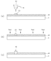


Classifications
-
- H—ELECTRICITY
- H10—SEMICONDUCTOR DEVICES; ELECTRIC SOLID-STATE DEVICES NOT OTHERWISE PROVIDED FOR
- H10F—INORGANIC SEMICONDUCTOR DEVICES SENSITIVE TO INFRARED RADIATION, LIGHT, ELECTROMAGNETIC RADIATION OF SHORTER WAVELENGTH OR CORPUSCULAR RADIATION
- H10F77/00—Constructional details of devices covered by this subclass
- H10F77/30—Coatings
- H10F77/306—Coatings for devices having potential barriers
- H10F77/311—Coatings for devices having potential barriers for photovoltaic cells
- H10F77/315—Coatings for devices having potential barriers for photovoltaic cells the coatings being antireflective or having enhancing optical properties
-
- H—ELECTRICITY
- H10—SEMICONDUCTOR DEVICES; ELECTRIC SOLID-STATE DEVICES NOT OTHERWISE PROVIDED FOR
- H10F—INORGANIC SEMICONDUCTOR DEVICES SENSITIVE TO INFRARED RADIATION, LIGHT, ELECTROMAGNETIC RADIATION OF SHORTER WAVELENGTH OR CORPUSCULAR RADIATION
- H10F10/00—Individual photovoltaic cells, e.g. solar cells
-
- H—ELECTRICITY
- H10—SEMICONDUCTOR DEVICES; ELECTRIC SOLID-STATE DEVICES NOT OTHERWISE PROVIDED FOR
- H10F—INORGANIC SEMICONDUCTOR DEVICES SENSITIVE TO INFRARED RADIATION, LIGHT, ELECTROMAGNETIC RADIATION OF SHORTER WAVELENGTH OR CORPUSCULAR RADIATION
- H10F71/00—Manufacture or treatment of devices covered by this subclass
-
- H—ELECTRICITY
- H10—SEMICONDUCTOR DEVICES; ELECTRIC SOLID-STATE DEVICES NOT OTHERWISE PROVIDED FOR
- H10F—INORGANIC SEMICONDUCTOR DEVICES SENSITIVE TO INFRARED RADIATION, LIGHT, ELECTROMAGNETIC RADIATION OF SHORTER WAVELENGTH OR CORPUSCULAR RADIATION
- H10F77/00—Constructional details of devices covered by this subclass
- H10F77/20—Electrodes
-
- H—ELECTRICITY
- H10—SEMICONDUCTOR DEVICES; ELECTRIC SOLID-STATE DEVICES NOT OTHERWISE PROVIDED FOR
- H10F—INORGANIC SEMICONDUCTOR DEVICES SENSITIVE TO INFRARED RADIATION, LIGHT, ELECTROMAGNETIC RADIATION OF SHORTER WAVELENGTH OR CORPUSCULAR RADIATION
- H10F77/00—Constructional details of devices covered by this subclass
- H10F77/20—Electrodes
- H10F77/206—Electrodes for devices having potential barriers
- H10F77/211—Electrodes for devices having potential barriers for photovoltaic cells
-
- Y—GENERAL TAGGING OF NEW TECHNOLOGICAL DEVELOPMENTS; GENERAL TAGGING OF CROSS-SECTIONAL TECHNOLOGIES SPANNING OVER SEVERAL SECTIONS OF THE IPC; TECHNICAL SUBJECTS COVERED BY FORMER USPC CROSS-REFERENCE ART COLLECTIONS [XRACs] AND DIGESTS
- Y02—TECHNOLOGIES OR APPLICATIONS FOR MITIGATION OR ADAPTATION AGAINST CLIMATE CHANGE
- Y02E—REDUCTION OF GREENHOUSE GAS [GHG] EMISSIONS, RELATED TO ENERGY GENERATION, TRANSMISSION OR DISTRIBUTION
- Y02E10/00—Energy generation through renewable energy sources
- Y02E10/50—Photovoltaic [PV] energy
Definitions
- the present invention relates to a method for forming a front electrode of a solar cell, and more particularly, when printing an etching solution in the step of etching the anti-reflection film, or when printing an electrode solution or a conductive solution for forming the front electrode, EHD, Electrohydrodynamic (Ink Jetting Type) solution is printed, by reducing the width of the front electrode printed on the semiconductor layer of the solar cell to provide a high aspect ratio front electrode, the light incident to the solar cell It relates to a method of forming a front electrode of a solar cell to increase the amount of.
- the solar cell is a device that converts light energy into electrical energy by using the photovoltaic effect. It has the advantages of pollution-free, indefinite resource, and semi-permanent life. It is expected to be an energy source that can be solved.
- Solar cells may be classified into silicon solar cells, thin film solar cells, dye-sensitized solar cells, organic polymer solar cells, and the like according to their constituent materials.
- crystalline silicon solar cells account for most of the total production of solar cells in the world, and the photoelectric conversion efficiency is higher than other cells, and the technology is continuously being developed, which is the most popular solar cell.
- a solar cell includes an n-type semiconductor layer on a front surface of a silicon substrate and a p-type semiconductor layer on a rear surface thereof to form a pn junction interface.
- the semiconductor layer S is formed to contain.
- An antireflection film AR is coated on the front surface of the semiconductor layer S to minimize reflection of light incident on the solar cell, and the front electrode FE is wired to contact the semiconductor layer S.
- the rear electrode BE is wired on the rear surface of the semiconductor layer S.
- the solar cell generates charges (holes, electrons) by the incident light, and the generated charges are separately collected through the front electrode FE and the rear electrode BE to generate electrical energy.
- the generated electrical energy increases.
- the distance between the front electrodes FE spaced apart from each other should be widened.
- a method of reducing the electrode width w of the front electrode FE has been sought to widen the interval between the front electrodes FE.
- the front electrode is used to reduce the electrode width (w) of the front electrode as the electrode solution having a viscosity of 30000 cp to 150000 cp is printed by a contact printing method such as screen printing. There is a limit.
- the amount of charge transferred through the front electrode is proportional to the cross-sectional area of the front electrode (the product of the electrode width (w) and the height of the electrode (h)), reducing the electrode width (w) at the same electrode height (h) There is a problem that the electrical resistance increases.
- the contact printing method such as screen printing has a problem in that the semiconductor layer is damaged during the process, and thus, non-contact printing such as ink jetting to eject ink through the nozzle Law is required.
- the maximum viscosity of the electrode solution discharged in piezoelectric ink jetting or thermoelectric ink jetting is about 30 cP, there is a limit in printing the electrode solution having the aforementioned viscosity (30000 cps to 150000 cps).
- the size of the solid particles contained in the electrode solution is nanoscale, there are problems such as clogging of the nozzle.
- the diameter of the nozzle may be expanded to prevent nozzle clogging, but when the diameter of the nozzle is expanded in the conventional ink jetting, it is difficult to implement a desired minute electrode width w.
- an object of the present invention is to solve such a conventional problem, by reducing the electrode width of the front electrode, and by increasing the distance between the adjacent front electrode, the solar cell which can increase the amount of light incident on the solar cell
- the present invention provides a method for forming a front electrode.
- the method of forming the front electrode of the solar cell can maintain or increase the amount of charge that is transferred through the front electrode, and can reduce the electrical resistance generated in the front electrode In providing.
- the present invention provides a method for forming a front electrode of a solar cell that can prevent damage to a semiconductor layer while using an electrode solution having a viscosity of 30000cp to 150000cp as it is.
- the present invention provides a method for forming a front electrode of a solar cell that can implement a desired minute electrode width.
- the present invention provides a method for forming a front electrode of a solar cell capable of forming a front electrode having a high aspect ratio.
- a method for forming a front electrode on the front surface of a semiconductor layer of a solar cell the electrode forming step of printing an electrode solution on the front surface of the semiconductor layer;
- the electrode solution is a material mixed with the adhesive for bonding the semiconductor layer and the metal, the metal for forming the front electrode, the electrode forming step is at least one electrohydrodynamic (EHD, Electrohydrodynamic ) Forming a front electrode of a solar cell, characterized in that the charge is applied to the electrode solution by a power source applied using an ink jetting type, and the electrode solution having a charge from the nozzle is discharged by an electrostatic force. Is achieved by the method.
- EHD Electrohydrodynamic
- a surface treatment step of applying an anti-reflection film to the entire surface of the semiconductor layer to prevent reflection loss of incident light It is preferable to further include.
- the object is, according to the present invention, a method for forming a front electrode on a solar cell coated with an antireflection film on the entire surface of the semiconductor layer, the etching step of printing an etching solution on the antireflection film; An electrode forming step of printing an electrode solution on a portion where the anti-reflection film is etched through the etching step; An electrode curing step of curing the electrode solution such that the electrode solution printed on the portion where the anti-reflection film is etched through the electrode forming step becomes the front electrode; Including, The electrode solution is a material mixed with an adhesive for bonding the semiconductor layer and the metal, and the metal for forming the front electrode, wherein the etching step and the electrode forming step is at least one electrohydrodynamic (EHD, Electrohydrodynamic) The etching solution and the electrode solution by applying a power applied by using the ink jetting type (Ink Jetting Type), each of the etching solution and the electrode having a charge in each nozzle with an electrostatic force It
- a method for forming a front electrode on a solar cell coated with an antireflection film on the entire surface of the semiconductor layer comprising: etching the antireflection film by dry etching using a laser or plasma; An electrode forming step of printing an electrode solution on a portion where the anti-reflection film is etched through the etching step; An electrode curing step of curing the electrode solution such that the electrode solution printed on the portion where the anti-reflection film is etched through the electrode forming step becomes the front electrode;
- the electrode solution is a material mixed with the adhesive for bonding the semiconductor layer and the metal, the metal for forming the front electrode, the electrode forming step is at least one electrohydrodynamic (EHD, Electrohydrodynamic ) Forming a front electrode of a solar cell, characterized in that the charge is applied to the electrode solution by a power source applied using an ink jetting type, and the electrode solution having a charge from the nozzle is discharged by an electrostatic force.
- EHD Electrohydrodynamic
- a hydrophobic layer is formed by applying a hydrophobic material on the antireflection film to form a hydrophobic layer step; An etching step of printing an etching solution on the hydrophobic layer; Removing the hydrophobic layer and applying heat to the hydrophobic layer so that the etching solution printed through the etching step etches the anti-reflection film; An electrode forming step of printing an electrode solution on a portion where the anti-reflection film is etched through the hydrophobic layer removing step; An electrode curing step of curing the electrode solution such that the electrode solution printed on the portion where the anti-reflection film is etched through the electrode forming step becomes the front electrode; Including, The electrode solution is a material mixed with an adhesive for bonding the semiconductor layer and the metal, and the metal for forming the front electrode, wherein the etching step and the electrode forming
- an electrode for printing a conductive solution mixed with an etching solution and an electrode solution on the antireflection film Forming step An electrode curing step of curing the conductive solution such that the conductive solution printed on the antireflection film becomes the front electrode through the electrode forming step;
- the electrode solution is a material mixed with the adhesive for bonding the semiconductor layer and the metal, the metal for forming the front electrode, the electrode forming step is at least one electrohydrodynamic (EHD, Electrohydrodynamic ) Forming a front electrode of a solar cell, characterized in that the charge is applied to the conductive solution by a power source applied using an ink jetting type, and the conductive solution having a charge from the nozzle is discharged by electrostatic force. Is achieved by the method.
- EHD Electrohydrodynamic
- a hydrophobic layer is formed by applying a hydrophobic material on the antireflection film to form a hydrophobic layer step;
- the electrode solution is a material mixed with the adhesive for bonding the semiconductor layer and the metal, the metal for forming the front electrode, the electrode forming step is at least one electrohydrodynamic (EHD, Electrohydrodynamic ) Forming a front electrode of a solar cell, characterized in that the charge is applied
- the object is, according to the present invention, a method for forming a front electrode on a solar cell coated with an antireflection film on the entire surface of the semiconductor layer, the etching step of printing an etching solution on the antireflection film;
- Including, but the etching step is to charge the etching solution by a power applied by using one or more times (EHD, Electrohydrodynamic) ink jetting type (EHD Jet Inking Type), the charge in the nozzle by the electrostatic force It is achieved by a method for forming a front electrode of a solar cell, characterized in that the etching solution having a discharge.
- a hydrophobic layer is formed by applying a hydrophobic material on the antireflection film to form a hydrophobic layer step; An etching step of printing an etching solution on the hydrophobic layer; Removing the hydrophobic layer and applying heat to the hydrophobic layer so that the etching solution printed through the etching step etches the anti-reflection film; An auxiliary electrode forming step of forming the front electrode on the portion where the anti-reflection film is etched through the hydrophobic layer removing step by at least one electroplating method; Including, wherein the electrode solution is a material mixed with the adhesive for bonding the semiconductor layer and the metal, and the metal for forming the front electrode, the etching step is at least one electrohydrodynamic (EHD, Electrohydrodynamic) A method of forming a front electrode of a solar cell, characterized in that charge
- auxiliary electrode forming step of performing at least one electroplating with a metal for forming the front electrode on the portion where the anti-reflection film is etched It is preferable to further include.
- a method for forming a front electrode of a solar cell which can increase the amount of light incident on the solar cell by reducing the electrode width of the front electrode and widening the distance between adjacent front electrodes.
- the method of forming the front electrode of the solar cell can maintain or increase the amount of charge that is transferred through the front electrode, and can reduce the electrical resistance generated in the front electrode This is provided.
- an electrode solution having a viscosity of 100 cps to 150000 cps may be used, and a method of forming a front electrode of a solar cell capable of preventing breakage of a semiconductor layer is provided.
- a method of forming a front electrode of a solar cell capable of realizing a desired fine electrode width is provided.
- a method for forming a front electrode of a solar cell capable of reducing the contact area of the printed solution and improving the reduction of the electrode width according to the printed solution.
- a method of forming a front electrode of a solar cell which improves precision of front electrode formation and secures a high aspect ratio of the front electrode, is provided.
- EHD electrohydrodynamic ink jetting type
- FIG. 1 is a view schematically showing the structure of a typical solar cell
- FIG. 2 is a flowchart illustrating a first method of forming a front electrode on a solar cell according to an embodiment of the present invention
- 3 and 4 are flowcharts for explaining a second method and a third method of forming a front electrode in a solar cell according to an embodiment of the present invention
- FIG. 5 is a process flow diagram for a second method of forming a front electrode on a solar cell according to one embodiment of the present invention.
- FIG. 6 is a process flow diagram for a third method of forming a front electrode on a solar cell according to one embodiment of the present invention.
- FIG. 7 is a flowchart illustrating a fourth method and a fifth method of forming a front electrode on a solar cell according to an embodiment of the present invention
- FIG. 8 is a flowchart illustrating a sixth method and a seventh method of forming a front electrode on a solar cell according to an embodiment of the present invention
- FIG. 9 is a process flow diagram for a sixth method of forming a front electrode on a solar cell according to one embodiment of the present invention.
- FIG. 10 is a process flow diagram for a seventh method of forming a front electrode on a solar cell according to one embodiment of the present invention.
- the semiconductor layer S is formed to include a pn junction interface by forming an n-type semiconductor layer on a front surface of a silicon substrate and a p-type semiconductor layer on a rear surface of the silicon substrate.
- the front surface of the semiconductor layer S is coated with an antireflection film AR, and the front electrode FE is wired to contact the semiconductor layer S.
- the rear electrode BE is wired on the rear surface of the semiconductor layer S.
- the solar cell generates charges (holes, electrons) by the incident light, and the generated charges are separately collected through the front electrode FE and the rear electrode BE to generate electrical energy.
- the electrohydrodynamic (EHD, Electrohydrodynamic) ink jetting Charge is applied to the solution by a power source applied using an ink jetting type, and a solution having a charge from the nozzle N is discharged by electrostatic force to be printed on the semiconductor layer S.
- EHD Electrohydrodynamic
- the electrode solution E2 when the antireflection film AR is applied to the semiconductor layer S, the electrode solution E2 must be printed after undergoing an etching step.
- the method of forming the front electrode of the solar cell according to the exemplary embodiment of the present invention is a method for forming the front electrode FE in the semiconductor layer S of the solar cell, and can be classified into seven methods as follows.
- the first method is a method of printing the electrode solution (E2) directly on the semiconductor layer (S), and curing the printed electrode solution (E2) to form a front electrode (FE) in the solar cell.
- the electrode solution E2 has a viscosity of about 100 cP to 150000 cP, and may be formed in the form of a paste.
- the electrode solution E2 is a material in which a metal for forming the front electrode FE and an adhesive for joining the ceramic (semiconductor layer S) and the metal are mixed.
- glass frit is used as an adhesive
- silver (Ag) is generally used as a metal for forming the front electrode FE, but the type of adhesive or metal is limited. no.
- FIG. 2 is a flowchart illustrating a first method of forming a front electrode on a solar cell according to an embodiment of the present invention.
- the first method of forming the front electrode FE in the solar cell includes a semiconductor forming step S1, an electrode forming step S7, and an electrode curing step S8.
- the semiconductor layer S is formed to generate charges (holes, electrons) by incident light.
- the semiconductor layer S is formed by forming an n-type semiconductor layer on the front surface of the silicon substrate and a p-type semiconductor layer on the rear surface thereof to include a pn junction interface. Then, the n-type semiconductor layer on the front surface acts as an emitter.
- the electrode forming step S7 is for forming the front electrode FE through which charges (holes, electrons) generated in the semiconductor layer S can move.
- the electrode solution E2 is printed on the entire surface of the semiconductor layer S formed through the semiconductor forming step S1. Since the electrode solution E2 forms the front electrode FE through the electrode curing step S8 described later, the electrode solution E2 should be printed in consideration of the pattern of the front electrode FE to be formed. In the electrode forming step S7, it is advantageous to be repeated one or more times in consideration of the electrode height h of the front electrode FE to be formed.
- the electrode solution E2 is charged by a power applied by using an electrohydrodynamic ink jetting type (EHD).
- the electrode solution E2 having the electric charge is discharged from the nozzle N by the electrostatic force.
- the electrode solution E2 may be discharged without clogging the nozzle N by using an electrohydrodynamic ink jetting type (EHD) even though the electrode solution E2 has a viscosity of about 1000 cp to 150000 cp.
- the electrode solution E2 having a viscosity of 20000 cp or more is discharged.
- the electrohydrodynamic ink jetting type may allow the size of the droplets discharged from the nozzle N to be smaller than the diameter of the nozzle N.
- FIG. Accordingly, when the above-described electrode solution E2 is discharged from the nozzle N, the droplet size of the discharged electrode solution E2 can be adjusted according to the applied power, and thus the electrode width of the front electrode FE to be formed. In consideration of (w), a desired electrode width w can be set.
- the electrode solution E2 printed on the semiconductor layer S is cured through the electrode forming step S7.
- the curing temperature of silver (Ag) in the metal for forming the front electrode (FE) in the electrode solution (E2) is about 200 degrees (°C)
- the curing temperature of the glass frit in the adhesive is about 700 degrees (°C). ) to be. Accordingly, in the electrode curing step S8, it is advantageous to heat the entire surface of the semiconductor layer S at 700 ° C. or more.
- the front electrode FE is formed on the entire surface of the semiconductor layer S.
- FIG. The electrode curing step S8 may be repeated one or more times in engagement with the electrode forming step S7 which is repeated in consideration of the height h of the front electrode FE to be formed.
- the first method of forming the front electrode FE on the solar cell may further include at least one of the surface treatment step S3 and the texturing step S2.
- an antireflection film AR is coated on the entire surface of the semiconductor layer S to prevent reflection of light incident to the solar cell and to prevent loss of incident light.
- the antireflection film AR may be coated on the entire surface of the semiconductor layer S to cover the front electrode FE stacked on the semiconductor layer S. In addition, it may be applied only between the front electrode FE formed in the semiconductor layer (S).
- the anti-reflection film AR formed in the surface treatment step S3 may use silicon nitride.
- the texturing step S2 irregularities are formed on the entire surface of the semiconductor layer S formed in the semiconductor forming step S1. If irregularities are formed on the entire surface of the semiconductor layer S through the texturing step S2, light absorption may be improved with respect to incident light, and the generation of charges (holes and electrons) may be promoted in the semiconductor layer S. have.
- the front surface of the semiconductor layer S may be hydrophilic to enhance adhesion between the semiconductor layer S and the anti-reflection film AR in the surface treatment step S3.
- the antireflection film AR is etched with the etching solution E1 while the antireflection film AR is formed on the semiconductor layer S, and then the electrode solution E2 is etched on the etched portion of the antireflection film AR. ), And the front electrode FE is formed on the solar cell by curing the printed electrode solution E2.
- the etching solution E1 may be a material capable of removing the contacted antireflection film AR.
- the electrode solution E2 has a viscosity of about 100 cP to 150000 cP, and may be formed in the form of a paste.
- the electrode solution E2 is a material in which a metal for forming the front electrode FE and an adhesive for joining the ceramic (semiconductor layer S) and the metal are mixed.
- glass frit is used as an adhesive
- silver (Ag) is generally used as a metal for forming the front electrode FE, but the type of adhesive or metal is limited. no.
- FIG. 3 and 4 are flowcharts illustrating a second method and a third method of forming a front electrode on a solar cell according to an embodiment of the present invention
- FIG. 5 is an embodiment according to an embodiment of the present invention. This is a process flow diagram for the second method of forming a front electrode in a cell.
- the semiconductor forming step S1 the surface treatment step S3, the etching step S5, and the electrode forming step (S7) and the electrode curing step (S8).
- the semiconductor layer S is formed to generate charges (holes, electrons) by incident light.
- the semiconductor layer S is formed by forming an n-type semiconductor layer on the front surface of the silicon substrate and a p-type semiconductor layer on the rear surface thereof to include a pn junction interface. Then, the n-type semiconductor layer on the front surface acts as an emitter.
- an antireflection film AR is coated on the entire surface of the semiconductor layer S to prevent reflection of light incident to the solar cell and to prevent loss of incident light.
- the antireflection film AR is applied to the entire surface of the semiconductor layer S.
- the anti-reflection film AR formed in the surface treatment step S3 may use silicon nitride.
- the etching solution E1 is printed on the antireflection film AR as shown in FIG. 5A. Then, as shown in (b) of FIG. 5, the antireflection film AR of the portion in contact with the etching solution E1 is etched to form a pattern for forming the front electrode FE.
- the etching step S5 may be repeated one or more times in consideration of the thickness of the antireflection film AR or the electrode width w of the front electrode FE to be formed.
- etching solution (E1) In order to print the etching solution (E1) in the etching step (S5), charge is applied to the etching solution (E1) by a power applied by using an electrohydrodynamic (EHD, Electro Hydrodynamic) ink jetting type (EHD), The etching solution E1 having an electric charge is discharged from the nozzle N by the electrostatic force.
- the etching solution E1 has a viscosity of about 100 cp or more or about 300 cp or more to be discharged by an electrohydrodynamic ink jetting type (EHD).
- the electrohydrodynamic ink jetting type (EHD) may allow the size of the droplets discharged from the nozzle N to be smaller than the diameter of the nozzle N.
- the droplet size of the etching solution E1 discharged according to the applied power can be adjusted, so that the electrode width w of the front electrode FE to be formed
- the anti-reflection film AR may be etched at a desired portion.
- the electrode forming step S7 is for forming the front electrode FE through which charges (holes, electrons) generated in the semiconductor layer S can move.
- the electrode forming step S7 prints the electrode solution E2 on the portion where the antireflection film AR is etched through the etching step S5 as shown in FIG. 5C. Since the electrode solution E2 forms the front electrode FE through the electrode curing step S8 described later, the electrode solution E2 should be printed in consideration of the pattern of the front electrode FE to be formed. In the electrode forming step S7, it is advantageous to be repeated one or more times in consideration of the electrode height h of the front electrode FE to be formed.
- the electrode solution E2 is charged by a power applied by using an electrohydrodynamic ink jetting type (EHD).
- the electrode solution E2 having the electric charge is discharged from the nozzle N by the electrostatic force.
- the electrode solution E2 may be discharged without clogging the nozzle N by using an electrohydrodynamic ink jetting type (EHD) even though the electrode solution E2 has a viscosity of about 1000 cp to 150000 cp.
- the electrode solution E2 having a viscosity of 20000 cp or more is discharged.
- the electrohydrodynamic ink jetting type may allow the size of the droplets discharged from the nozzle N to be smaller than the diameter of the nozzle N.
- FIG. Accordingly, when the above-described electrode solution E2 is discharged from the nozzle N, the droplet size of the discharged electrode solution E2 can be adjusted according to the applied power, and thus the electrode width of the front electrode FE to be formed. In consideration of (w), a desired electrode width w can be set.
- the electrode forming step S7 when the above-described etching step S5 etches the antireflection film AR by dry etching using a laser or plasma, the electrode forming step S7 must be performed using an electrohydrodynamic ink jetting method (EHD). Ink Jetting Type) is used.
- EHD electrohydrodynamic ink jetting Type
- the electrode curing step S8 cures the electrode solution E2 printed on the portion where the anti-reflection film AR is etched through the electrode forming step S7.
- the curing temperature of silver (Ag) in the metal for forming the front electrode (FE) in the electrode solution (E2) is about 200 degrees (°C)
- the curing temperature of the glass frit in the adhesive is about 700 degrees (°C). ) to be. Accordingly, in the electrode curing step S8, it is advantageous to heat the entire surface of the semiconductor layer S at 700 ° C. or higher as shown in FIG. 5D.
- the glass frit in the adhesive causes an oxidation reaction with silicon nitride (nitride) used as the antireflection film (AR) during the curing process, thereby causing the antireflection film (AR) to be etched. You can get it.
- the front electrode FE is formed on the entire surface of the semiconductor layer S as shown in FIG.
- the electrode curing step S8 may be repeated one or more times in engagement with the electrode forming step S7 which is repeated in consideration of the height h of the front electrode FE to be formed.
- the second method of forming the front electrode FE in the solar cell may further include at least one of the texturing step S2 and the auxiliary electrode forming step S7-1.
- the texturing step S2 irregularities are formed on the entire surface of the semiconductor layer S formed in the semiconductor forming step S1. If irregularities are formed on the entire surface of the semiconductor layer S through the texturing step S2, light absorption may be improved with respect to incident light, and the generation of charges (holes and electrons) may be promoted in the semiconductor layer S. have.
- the front surface of the semiconductor layer S may be hydrophilic to enhance adhesion between the semiconductor layer S and the anti-reflection film AR in the surface treatment step S3.
- the auxiliary electrode forming step S7-1 is to form the front electrode FE through which charges (holes, electrons) generated in the semiconductor layer S can move.
- the metal for forming the front electrode FE is formed by electroplating on a portion where the anti-reflection film AR is etched through the etching step S5 as shown in FIG. 3. May be plated.
- the auxiliary electrode forming step (S7-1) is a method of electroplating the electrode solution (E2) cured in the portion where the anti-reflection film (AR) is etched through the electrode curing step (S8) as shown in FIG.
- the metal for forming the front electrode FE may be plated.
- the electrical conductivity may be improved by increasing the purity of the front electrode FE.
- the third method is to apply the hydrophobic layer HP on the antireflection film AR in a state where the antireflection film AR is formed on the semiconductor layer S, and then print the etching solution E1 on the hydrophobic layer HP. Then, the etching solution E1 etches the antireflection film AR while the hydrophobic layer HP is removed, the electrode solution E2 is printed on the etched portion of the antireflection film AR, and the printed electrode solution E2 is printed. ) To form a front electrode (FE) in the solar cell.
- FE front electrode
- the material forming the hydrophobic layer (HP) may be an organic compound consisting of monohydric or dihydric alcohol fatty acid esters, it may be used a wax containing an alkyl chain (alkyl chain).
- the etching solution E1 is sufficient to be a material capable of removing the antireflection film AR in contact.
- the electrode solution E2 has a viscosity of about 100 cP to 150000 cP, and may be formed in the form of a paste.
- the electrode solution E2 is a material in which a metal for forming the front electrode FE and an adhesive for joining the ceramic (semiconductor layer S) and the metal are mixed.
- glass frit is used as an adhesive
- silver (Ag) is generally used as a metal for forming the front electrode FE, but the type of adhesive or metal is limited. no.
- FIG. 3 and 4 are flowcharts illustrating a second method and a third method of forming a front electrode in a solar cell according to an embodiment of the present invention
- FIG. 6 is an embodiment according to an embodiment of the present invention.
- the semiconductor forming step S1 the surface treatment step S3, the hydrophobic lamination step S4, , An etching step S5, a hydrophobic layer removing step S6, an electrode forming step S7, and an electrode curing step S8.
- the semiconductor layer S is formed to generate charges (holes, electrons) by incident light.
- the n-type semiconductor layer is formed on the front surface of the silicon substrate and the p-type semiconductor layer is formed on the rear surface of the semiconductor substrate to form the pn junction interface. Then, the n-type semiconductor layer on the front surface acts as an emitter.
- an antireflection film AR is coated on the entire surface of the semiconductor layer S to prevent reflection of light incident to the solar cell and to prevent loss of incident light.
- the antireflection film AR may be applied to the entire surface of the semiconductor layer S.
- the anti-reflection film AR formed in the surface treatment step S3 may use silicon nitride.
- a hydrophobic material is coated on the antireflection film AR to form a hydrophobic layer HP.
- the hydrophobic layer HP formed on the anti-reflection film AR through the hydrophobic lamination step S4 is evaporated at a low temperature (lower than the temperature for curing the electrode solution), and is soluble in water-soluble (water soluble) or oily solvents. It is advantageous to have the property of not dissolving.
- heat may be applied to the hydrophobic material, and the heated hydrophobic material may be sprayed onto the antireflection film AR.
- the etching solution E1 is printed on the hydrophobic layer HP as shown in FIG. 6B.
- the contact area between the hydrophilic etching solution E1 and the hydrophobic layer HP can be reduced.
- the etching width of the antireflection film AR may be reduced, and the electrode of the front electrode FE formed on the etched portion of the antireflection film AR as the etching width of the antireflection film AR is reduced.
- the width w may also be reduced, thereby increasing the amount of light incident on the solar cell.
- etching solution (E1) In order to print the etching solution (E1) in the etching step (S5), charge is applied to the etching solution (E1) by a power applied by using an electrohydrodynamic (EHD, Electro Hydrodynamic) ink jetting type (EHD), The etching solution E1 having an electric charge is discharged from the nozzle N by the electrostatic force.
- the etching solution E1 has a viscosity of about 100 cps or more or about 300 cps or more and is discharged without clogging of the nozzle N by an electrohydrodynamic ink jetting type (EHD).
- the electrohydrodynamic ink jetting type (EHD) may allow the size of the droplets discharged from the nozzle N to be smaller than the diameter of the nozzle N.
- the droplet size of the etching solution E1 discharged according to the applied power can be adjusted, so that the electrode width of the front electrode FE to be formed
- the antireflection film AR may be etched at a desired portion.
- the hydrophobic layer removing step S6 applies heat to the hydrophobic layer HP.
- the hydrophobic layer HP is heated, the hydrophobic layer HP is removed by the heat applied as shown in FIG. 6C, and the etching solution printed through the etching step S5 is printed.
- a pattern for forming the front electrode FE by E1 etches the antireflection film AR.
- the etching solution E1 is further added to the etched portion of the antireflection film AR from which the hydrophobic layer HP is removed in consideration of the thickness of the antireflection film AR or the electrode width w of the front electrode FE to be formed.
- the temperature of the heat applied to the hydrophobic layer HP in the hydrophobic layer removing step S6 is advantageously lower than the curing temperature of the metal for forming the front electrode FE, which will be described later, or the curing temperature of the electrode solution E2.
- the electrode forming step S7 is for forming the front electrode FE through which charges (holes, electrons) generated in the semiconductor layer S can move.
- the electrode solution E2 is printed on the portion where the anti-reflection film AR is etched through the hydrophobic layer removing step S6 as shown in FIG. 6D. Since the electrode solution E2 forms the front electrode FE through the electrode curing step S8 described later, the electrode solution E2 should be printed in consideration of the pattern of the front electrode FE to be formed. In the electrode forming step S7, it is advantageous to be repeated one or more times in consideration of the electrode height h of the front electrode FE to be formed.
- the electrode solution E2 is charged by a power applied by using an electrohydrodynamic ink jetting type (EHD).
- the electrode solution E2 having the electric charge is discharged from the nozzle N by the electrostatic force.
- the electrode solution E2 may be discharged without clogging the nozzle N by using an electrohydrodynamic ink jetting type (EHD) even though the electrode solution E2 has a viscosity of about 1000 cp to 150000 cp.
- the electrode solution E2 having a viscosity of 20000 cp or more is discharged.
- the electrohydrodynamic ink jetting type may allow the size of the droplets discharged from the nozzle N to be smaller than the diameter of the nozzle N.
- FIG. Accordingly, when the above-described electrode solution E2 is discharged from the nozzle N, the droplet size of the discharged electrode solution E2 can be adjusted according to the applied power, and thus the electrode width of the front electrode FE to be formed. In consideration of (w), a desired electrode width w can be set.
- the electrode curing step S8 cures the electrode solution E2 printed on the portion where the anti-reflection film AR is etched through the electrode forming step S7.
- the curing temperature of silver (Ag) in the metal for forming the front electrode (FE) in the electrode solution (E2) is about 200 degrees (°C)
- the curing temperature of the glass frit in the adhesive is about 700 degrees (°C). ) to be. Accordingly, in the electrode curing step S8, it is advantageous to heat the entire surface of the semiconductor layer S at 700 ° C. or higher as shown in FIG. 6E.
- the glass frit in the adhesive causes an oxidation reaction with silicon nitride (nitride) used as the antireflection film (AR) during the curing process, thereby causing the antireflection film (AR) to be etched. You can get it.
- the front electrode FE is formed on the entire surface of the semiconductor layer S as shown in FIG.
- the electrode curing step S8 may be repeated one or more times in engagement with the electrode forming step S7 which is repeated in consideration of the height h of the front electrode FE to be formed.
- the third method of forming the front electrode FE on the solar cell may further include at least one of the texturing step S2 and the auxiliary electrode forming step S7-1.
- the texturing step S2 irregularities are formed on the entire surface of the semiconductor layer S formed in the semiconductor forming step S1. If irregularities are formed on the entire surface of the semiconductor layer S through the texturing step S2, light absorption may be improved with respect to incident light, and the generation of charges (holes and electrons) may be promoted in the semiconductor layer S. have.
- the front surface of the semiconductor layer S may be hydrophilic to enhance adhesion between the semiconductor layer S and the anti-reflection film AR in the surface treatment step S3.
- the auxiliary electrode forming step S7-1 is to form the front electrode FE through which charges (holes, electrons) generated in the semiconductor layer S can move.
- the metal for forming the front electrode FE by electroplating is formed on the portion where the anti-reflection film AR is etched through the hydrophobic layer removing step S6 as shown in FIG. 3. Can be plated.
- the auxiliary electrode forming step (S7-1) is a method of electroplating the electrode solution (E2) cured in the portion where the anti-reflection film (AR) is etched through the electrode curing step (S8) as shown in FIG.
- the metal for forming the front electrode FE may be plated.
- the electrical conductivity may be improved by increasing the purity of the front electrode FE.
- the anti-reflection film AR is etched with the etching solution E1 while the anti-reflection film AR is formed on the semiconductor layer S, and then the front electrode FE is etched on the etched portion of the anti-reflection film AR.
- the etching solution E1 may be a material capable of removing the contacted antireflection film AR.
- silver (Ag) is normally used as a metal for forming the front electrode FE, the type of the adhesive or the metal is not limited thereto.
- FIG. 7 is a flowchart illustrating a fourth method and a fifth method of forming a front electrode on a solar cell according to an embodiment of the present invention.
- the semiconductor forming step S1 the surface treatment step S3, the etching step S5, and the auxiliary electrode forming step S7. -1).
- the semiconductor layer S is formed to generate charges (holes, electrons) by incident light.
- the semiconductor layer S is formed by forming an n-type semiconductor layer on the front surface of the silicon substrate and a p-type semiconductor layer on the rear surface thereof to include a pn junction interface. Then, the n-type semiconductor layer on the front surface acts as an emitter.
- an antireflection film AR is coated on the entire surface of the semiconductor layer S to prevent reflection of light incident to the solar cell and to prevent loss of incident light.
- the antireflection film AR may be coated on the entire surface of the semiconductor layer S.
- the anti-reflection film AR formed in the surface treatment step S3 may use silicon nitride.
- the etching solution E1 is printed on the antireflection film AR as shown in FIG. 5A. Then, as shown in (b) of FIG. 5, the antireflection film AR of the portion in contact with the etching solution E1 is etched to form a pattern for forming the front electrode FE.
- the etching step S5 may be repeated one or more times in consideration of the thickness of the antireflection film AR or the electrode width w of the front electrode FE to be formed.
- etching solution (E1) In order to print the etching solution (E1) in the etching step (S5), charge is applied to the etching solution (E1) by a power applied by using an electrohydrodynamic (EHD, Electro Hydrodynamic) ink jetting type (EHD), The etching solution E1 having an electric charge is discharged from the nozzle N by the electrostatic force.
- the etching solution E1 has a viscosity of about 100 cps or more or about 300 cps or more and is discharged without clogging of the nozzle N by an electrohydrodynamic ink jetting type (EHD).
- the electrohydrodynamic ink jetting type (EHD) may allow the size of the droplets discharged from the nozzle N to be smaller than the diameter of the nozzle N.
- the droplet size of the etching solution E1 discharged according to the applied power can be adjusted, so that the electrode width of the front electrode FE to be formed
- the antireflection film AR may be etched at a desired portion.
- the auxiliary electrode forming step S7-1 is to form the front electrode FE through which charges (holes, electrons) generated in the semiconductor layer S can move.
- the metal for forming the front electrode FE may be plated on the portion where the anti-reflection film AR is etched through the etching step S5 by electroplating.
- the electrical conductivity may be improved by increasing the purity of the front electrode FE.
- the fourth method of forming the front electrode FE in the solar cell may further include a texturing step (S2).
- the texturing step S2 irregularities are formed on the entire surface of the semiconductor layer S formed in the semiconductor forming step S1. If irregularities are formed on the entire surface of the semiconductor layer S through the texturing step S2, light absorption may be improved with respect to incident light, and the generation of charges (holes and electrons) may be promoted in the semiconductor layer S. have.
- the front surface of the semiconductor layer S may be hydrophilic to enhance adhesion between the semiconductor layer S and the anti-reflection film AR in the surface treatment step S3.
- the fifth method is to apply a hydrophobic layer (HP) on the antireflection film (AR) in a state where the antireflection film (AR) is formed on the semiconductor layer (S), and then print the etching solution (E1) on the hydrophobic layer (HP).
- the hydrophobic layer HP is removed, the printed etching solution E1 etches the antireflection film AR, and the metal for forming the front electrode FE is plated on the etched portion of the antireflection film AR.
- the front electrode FE is formed on a solar cell.
- the material forming the hydrophobic layer HP may be an organic compound consisting of monohydric or dihydric alcohol fatty acid esters. It is also possible to use a wax containing an alkyl chain.
- the etching solution E1 is sufficient to be a material capable of removing the antireflection film AR in contact.
- silver (Ag) is normally used as a metal for forming the front electrode FE, the type of the adhesive or the metal is not limited thereto.
- FIG. 7 is a flowchart illustrating a fourth method and a fifth method of forming a front electrode on a solar cell according to an embodiment of the present invention.
- the semiconductor forming step S1 the surface treatment step S3, the hydrophobic lamination step S4, and the etching step S5 are performed. And a hydrophobic layer removing step S6 and an auxiliary electrode forming step S7-1.
- the semiconductor layer S is formed to generate charges (holes, electrons) by incident light.
- the semiconductor layer S is formed by forming an n-type semiconductor layer on the front surface of the silicon substrate and a p-type semiconductor layer on the rear surface thereof to include a pn junction interface. Then, the n-type semiconductor layer on the front surface acts as an emitter.
- an antireflection film AR is coated on the entire surface of the semiconductor layer S to prevent reflection of light incident to the solar cell and to prevent loss of incident light.
- the antireflection film AR may be coated on the entire surface of the semiconductor layer S.
- the anti-reflection film AR formed in the surface treatment step S3 may use silicon nitride.
- a hydrophobic material is coated on the antireflection film AR to form a hydrophobic layer HP.
- the hydrophobic layer HP formed on the antireflection film AR through the hydrophobic lamination step S4 is advantageously evaporated at a low temperature and has a property of being insoluble in water (soluble easily in water) or in an oily solvent.
- heat is applied to the hydrophobic material, and the heated hydrophobic material is sprayed onto the antireflection film AR.
- the etching solution E1 is printed on the hydrophobic layer HP as shown in FIG. 6B.
- the contact area between the hydrophilic etching solution E1 and the hydrophobic layer HP can be reduced.
- the etching width of the antireflection film AR may be reduced, and the electrode of the front electrode FE formed on the etched portion of the antireflection film AR as the etching width of the antireflection film AR is reduced.
- the width w may also be reduced, thereby increasing the amount of light incident on the solar cell.
- etching solution (E1) In order to print the etching solution (E1) in the etching step (S5), charge is applied to the etching solution (E1) by a power applied by using an electrohydrodynamic (EHD, Electro Hydrodynamic) ink jetting type (EHD), The etching solution E1 having an electric charge is discharged from the nozzle N by the electrostatic force.
- the etching solution E1 has a viscosity of about 100 cps or more or about 300 cps or more and is discharged without clogging of the nozzle N by an electrohydrodynamic ink jetting type (EHD).
- the electrohydrodynamic ink jetting type (EHD) may allow the size of the droplets discharged from the nozzle N to be smaller than the diameter of the nozzle N.
- the droplet size of the etching solution E1 discharged according to the applied power can be adjusted, so that the electrode width of the front electrode FE to be formed
- the antireflection film AR may be etched at a desired portion.
- the hydrophobic layer removing step S6 applies heat to the hydrophobic layer HP.
- the hydrophobic layer HP is heated, the hydrophobic layer HP is removed by the heat applied as shown in FIG. 6C, and the etching solution printed through the etching step S5 is printed.
- a pattern for forming the front electrode FE by E1 etches the antireflection film AR.
- the etching solution E1 is further added to the etched portion of the antireflection film AR from which the hydrophobic layer HP is removed in consideration of the thickness of the antireflection film AR or the electrode width w of the front electrode FE to be formed.
- the temperature of the heat applied to the hydrophobic layer HP in the hydrophobic layer removing step S6 is advantageously lower than the curing temperature of the metal for forming the front electrode FE, which will be described later, or the curing temperature of the electrode solution E2.
- the auxiliary electrode forming step S7-1 is to form the front electrode FE through which charges (holes, electrons) generated in the semiconductor layer S can move.
- the metal for forming the front electrode FE may be plated on the portion where the anti-reflection film AR is etched through the hydrophobic layer removing step S6.
- the electrical conductivity may be improved by increasing the purity of the front electrode FE.
- the fifth method of forming the front electrode FE in the solar cell may further include a texturing step (S2).
- the texturing step S2 irregularities are formed on the entire surface of the semiconductor layer S formed in the semiconductor forming step S1. If irregularities are formed on the entire surface of the semiconductor layer S through the texturing step S2, light absorption may be improved with respect to incident light, and the generation of charges (holes and electrons) may be promoted in the semiconductor layer S. have.
- the front surface of the semiconductor layer S may be hydrophilic to enhance adhesion between the semiconductor layer S and the anti-reflection film AR in the surface treatment step S3.
- the sixth method prints a conductive solution E3 in which the etching solution E1 and the electrode solution E2 are mixed directly on the antireflection film AR while the antireflection film AR is formed on the semiconductor layer S.
- the etching solution E1 mixed in the printed conductive solution E3 is to etch the antireflection film AR, and the electrode solution E2 mixed in the printed conductive solution E3 is etched in the antireflection film AR.
- the front electrode (FE) is formed on the solar cell by curing at the portion.
- the etching solution E1 mixed with the conductive solution E3 may be a material capable of removing the contacted antireflection film AR.
- the conductive solution (E3) has a viscosity of about 100 cP to 150000 cP, it may be formed in the form of a paste (paste).
- the electrode solution E2 mixed in the conductive solution E3 is a material in which a metal for forming the front electrode FE and an adhesive for joining the ceramic (semiconductor layer S) and the metal are mixed.
- glass frit is used as an adhesive
- silver (Ag) is generally used as a metal for forming the front electrode FE, but the type of adhesive or metal is limited. no.
- FIG. 8 is a flowchart illustrating a sixth method and a seventh method of forming a front electrode in a solar cell according to an embodiment of the present invention
- FIG. 9 is a front view of the solar cell according to an embodiment of the present invention.
- the semiconductor forming step S1 the surface treatment step S3, the electrode forming step S7, and the electrode curing Step S8 is included.
- the semiconductor layer S is formed to generate charges (holes, electrons) by incident light.
- the semiconductor layer S is formed by forming an n-type semiconductor layer on the front surface of the silicon substrate and a p-type semiconductor layer on the rear surface thereof to include a pn junction interface. Then, the n-type semiconductor layer on the front surface acts as an emitter.
- an antireflection film AR is coated on the entire surface of the semiconductor layer S to prevent reflection of light incident to the solar cell and to prevent loss of incident light.
- the antireflection film AR may be coated on the entire surface of the semiconductor layer S.
- FIG. The anti-reflection film AR formed in the surface treatment step S3 may use silicon nitride.
- the electrode forming step S7 is for forming the front electrode FE through which charges (holes, electrons) generated in the semiconductor layer S can move.
- the etching solution E1 is formed according to the pattern of the front electrode FE at the portion where the antireflection film AR is formed through the surface treatment step S3 as shown in FIG. 9A.
- the conductive solution E3 mixed with the electrode solution E2 is printed. Since the conductive solution E3 forms the front electrode FE while going through the electrode curing step S8 to be described later, it should be printed in consideration of the pattern of the front electrode FE to be formed.
- the conductive solution E3 in the electrode forming step (S7) to give a charge to the conductive solution (E3) by a power applied by using an electrohydrodynamic (EHD, Electro Hydrodynamic) ink jetting type (EHD)
- EHD Electro Hydrodynamic
- the conductive solution E3 having a charge is discharged from the nozzle N by the electrostatic force.
- the electrode solution E2 may be discharged without clogging the nozzle N by using an electrohydrodynamic ink jetting type (EHD) even though the electrode solution E2 has a viscosity of about 1000 cp to 150000 cp.
- the electrode solution E2 having a viscosity of 20000 cp or more is discharged.
- the electrohydrodynamic ink jetting type may allow the size of the droplets discharged from the nozzle N to be smaller than the diameter of the nozzle N.
- FIG. Accordingly, when the above-described conductive solution E3 is discharged from the nozzle N, the droplet size of the conductive solution E3 discharged can be adjusted according to the applied power, and thus the electrode width of the front electrode FE to be formed. In consideration of (w), a desired electrode width w can be set.
- the conductive solution E3 printed on the antireflection film AR is cured through the electrode forming step S7.
- the curing temperature of silver (Ag) in the metal for forming the front electrode (FE) in the electrode solution (E2) mixed in the conductive solution (E3) is about 200 degrees (° C), and the glass frit in the adhesive
- the curing temperature is about 700 degrees Celsius. Accordingly, in the electrode curing step S8, it is advantageous to heat the entire surface of the semiconductor layer S at 700 ° C. or more, as shown in FIG. 9B.
- the etching solution E1 mixed in the conductive solution E3 etches the anti-reflection film AR, and at the same time, the electrode solution E2 mixed in the conductive solution E3 is cured in the etched portion.
- the glass frit in the adhesive causes an oxidation reaction with silicon nitride (nitride) used as the antireflection film (AR) during the curing process, thereby causing the antireflection film (AR) to be etched. You can get it.
- the front electrode FE is formed on the entire surface of the semiconductor layer S as shown in FIG. 9C.
- the electrode curing step S8 may be repeated one or more times in engagement with the electrode forming step S7 which is repeated in consideration of the height h of the front electrode FE to be formed.
- the sixth method of forming the front electrode FE in the solar cell may further include at least one of the texturing step S2 and the auxiliary electrode forming step S7-1.
- the texturing step S2 irregularities are formed on the entire surface of the semiconductor layer S formed in the semiconductor forming step S1. If irregularities are formed on the entire surface of the semiconductor layer S through the texturing step S2, light absorption may be improved with respect to incident light, and the generation of charges (holes and electrons) may be promoted in the semiconductor layer S. have.
- the front surface of the semiconductor layer S may be hydrophilic to enhance adhesion between the semiconductor layer S and the anti-reflection film AR in the surface treatment step S3.
- the auxiliary electrode forming step S7-1 is to form the front electrode FE through which charges (holes, electrons) generated in the semiconductor layer S can move.
- Auxiliary electrode forming step (S7-1) is to form the front electrode (FE) by the electroplating method in the conductive solution (E3) cured in the portion where the anti-reflection film (AR) is etched through the electrode curing step (S8) The metal may be plated.
- the electrical conductivity may be improved by increasing the purity of the front electrode FE.
- the seventh method is to apply the hydrophobic layer (HP) on the antireflection film (AR) in the state in which the antireflection film (AR) is formed on the semiconductor layer (S), then the etching solution (E1) and the electrode solution on the hydrophobic layer (HP) Print the conductive solution (E3) mixed with (E2).
- the etching solution E1 mixed with the conductive solution E3 is etched while the hydrophobic layer HP is removed, and the anti-reflection film AR is mixed with the electrode solution E2 mixed with the conductive solution E3.
- the front electrode FE is formed on the solar cell by curing at an etched portion of the solar cell.
- the material forming the hydrophobic layer HP may be an organic compound consisting of monohydric or dihydric alcohol fatty acid esters. It is also possible to use a wax containing an alkyl chain.
- the etching solution E1 mixed with the conductive solution E3 may be a material capable of removing the contacted antireflection film AR.
- the conductive solution (E3) has a viscosity of about 100 cP to 150000 cP, it may be formed in the form of a paste (paste).
- the electrode solution E2 mixed in the conductive solution E3 is a material in which a metal for forming the front electrode FE and an adhesive for joining the ceramic (semiconductor layer S) and the metal are mixed. In an embodiment of the present invention, glass frit is used as an adhesive, and silver (Ag) is generally used as a metal for forming the front electrode FE, but the type of adhesive or metal is limited. no.
- FIG. 8 is a flowchart illustrating a sixth method and a seventh method of forming a front electrode on a solar cell according to an embodiment of the present invention
- FIG. 10 is a front view of the solar cell according to an embodiment of the present invention. Process flow diagram for the seventh method of forming an electrode.
- the semiconductor formation step S1 the surface treatment step S3, the hydrophobic lamination step S4, and the electrode formation are performed.
- a step S7, a hydrophobic layer removing step S6, and an electrode curing step S8 are included.
- the semiconductor layer S is formed to generate charges (holes, electrons) by incident light.
- the semiconductor layer S is formed by forming an n-type semiconductor layer on the front surface of the silicon substrate and a p-type semiconductor layer on the rear surface thereof to include a pn junction interface. Then, the n-type semiconductor layer on the front surface acts as an emitter.
- an antireflection film AR is coated on the entire surface of the semiconductor layer S to prevent reflection of light incident to the solar cell and to prevent loss of incident light.
- the antireflection film AR may be coated on the entire surface of the semiconductor layer S.
- FIG. The anti-reflection film AR formed in the surface treatment step S3 may use silicon nitride.
- a hydrophobic material is coated on the antireflection film AR to form a hydrophobic layer HP.
- the hydrophobic layer HP formed on the antireflection film AR through the hydrophobic lamination step S4 is advantageously evaporated at a low temperature and has a property of being insoluble in water (soluble easily in water) or in an oily solvent.
- heat is applied to the hydrophobic material, and the heated hydrophobic material is sprayed onto the antireflection film AR.
- the electrode forming step S7 is for forming the front electrode FE through which charges (holes, electrons) generated in the semiconductor layer S can move.
- the electrode forming step is performed by using the etching solution E1 and the electrode solution according to the pattern of the front electrode FE on the portion where the hydrophobic layer HP is formed through the hydrophobic lamination step S4.
- the conductive solution E3 mixed with E2) is printed. Then, the contact area between the hydrophilic (hidrophilic) conductive solution E3 and the hydrophobic layer HP can be reduced.
- the etching width of the antireflection film AR may be reduced, and as the etching width of the antireflection film AR is reduced, the electrode of the front electrode FE formed at the portion where the antireflection film AR is etched is formed.
- the width w may also be reduced, thereby increasing the amount of light incident on the solar cell.
- the conductive solution E3 forms the front electrode FE while going through the electrode curing step S8 to be described later, it should be printed in consideration of the pattern of the front electrode FE to be formed.
- the electrode forming step S7 it is advantageous to be repeated one or more times in consideration of the electrode height h of the front electrode FE to be formed.
- the conductive solution E3 in the electrode forming step (S7) to give a charge to the conductive solution (E3) by a power applied by using an electrohydrodynamic (EHD, Electro Hydrodynamic) ink jetting type (EHD)
- EHD Electro Hydrodynamic
- the conductive solution E3 having a charge is discharged from the nozzle N by the electrostatic force.
- the electrode solution E2 may be discharged without clogging the nozzle N by using an electrohydrodynamic ink jetting type (EHD) even though the electrode solution E2 has a viscosity of about 1000 cp to 150000 cp.
- the electrode solution E2 having a viscosity of 20000 cp or more is discharged.
- the electrohydrodynamic ink jetting type may allow the size of the droplets discharged from the nozzle N to be smaller than the diameter of the nozzle N.
- FIG. Accordingly, when the above-described conductive solution E3 is discharged from the nozzle N, the droplet size of the conductive solution E3 discharged can be adjusted according to the applied power, and thus the electrode width of the front electrode FE to be formed. In consideration of (w), a desired electrode width w can be set.
- the hydrophobic layer removing step S6 applies heat to the hydrophobic layer HP.
- the hydrophobic layer HP is heated, the hydrophobic layer HP is removed by the applied heat, and the conductive solution E3 printed through the electrode forming step comes into contact with the antireflection film AR. .
- the temperature of the heat applied to the hydrophobic layer HP in the hydrophobic layer removing step S6 is advantageously lower than the curing temperature of the metal for forming the front electrode FE, which will be described later, or the curing temperature of the electrode solution E2.
- the electrode curing step S8 cures the conductive solution E3 in contact with the antireflection film AR through the hydrophobic layer removing step S6.
- the curing temperature of silver (Ag) in the metal for forming the front electrode (FE) in the electrode solution (E2) mixed in the conductive solution (E3) is about 200 degrees (° C), and the glass frit in the adhesive
- the curing temperature is about 700 degrees Celsius. Accordingly, in the electrode curing step S8, as shown in FIG. 10C, it is advantageous to heat the entire surface of the semiconductor layer S to 700 ° C. or more.
- the etching solution E1 mixed in the conductive solution E3 etches the anti-reflection film AR, and at the same time, the electrode solution E2 mixed in the conductive solution E3 is cured in the etched portion.
- the glass frit in the adhesive causes an oxidation reaction with silicon nitride (nitride) used as the antireflection film (AR) during the curing process, thereby causing the antireflection film (AR) to be etched. You can get it.
- the front electrode FE is formed on the entire surface of the semiconductor layer S as shown in FIG.
- the electrode curing step S8 may be repeated one or more times in engagement with the electrode forming step S7 which is repeated in consideration of the height h of the front electrode FE to be formed.
- the hydrophobic layer removing step and the electrode curing step may be simultaneously performed under one temperature condition by heating the entire surface of the semiconductor layer S to 700 ° C or more.
- the seventh method of forming the front electrode FE in the solar cell may further include at least one of the texturing step S2 and the auxiliary electrode forming step S7-1.
- the texturing step S2 irregularities are formed on the entire surface of the semiconductor layer S formed in the semiconductor forming step S1. If irregularities are formed on the entire surface of the semiconductor layer S through the texturing step S2, light absorption may be improved with respect to incident light, and the generation of charges (holes and electrons) may be promoted in the semiconductor layer S. have.
- the front surface of the semiconductor layer S may be hydrophilic to enhance adhesion between the semiconductor layer S and the anti-reflection film AR in the surface treatment step S3.
- the auxiliary electrode forming step S7-1 is to form the front electrode FE through which charges (holes, electrons) generated in the semiconductor layer S can move.
- Auxiliary electrode forming step (S7-1) is to form the front electrode (FE) by the electroplating method in the conductive solution (E3) cured in the portion where the anti-reflection film (AR) is etched through the electrode curing step (S8) The metal may be plated.
- the electrical conductivity may be improved by increasing the purity of the front electrode FE.
- the present invention by reducing the electrode width of the front electrode and widening the distance between adjacent front electrodes, it is possible to increase the amount of light incident on the solar cell, by increasing the height of the electrode by reducing the electrode width, the front electrode Provided is a method of forming a front electrode of a solar cell, which can maintain or increase the amount of charge transferred through it, and can reduce the electrical resistance generated at the front electrode.
Landscapes
- Photovoltaic Devices (AREA)
- Electrodes Of Semiconductors (AREA)
Abstract
Le procédé de formation d'une électrode avant d'une cellule solaire selon la présente invention se rapporte à un processus consistant à former une électrode avant sur la surface d'une couche semi-conductrice d'une cellule solaire. Le procédé de formation d'une électrode avant sur la surface avant de la couche semi-conductrice d'une cellule solaire comprend les étapes consistant à : imprimer une solution d'électrode sur la surface avant de la couche semi-conductrice pour former l'électrode ; et durcir ladite solution d'électrode de sorte que ladite solution d'électrode imprimée sur ladite couche semi-conductrice lors de ladite étape de formation d'électrode configure ladite électrode avant. Ladite solution d'électrode est formée par le mélange d'un agent de liaison destiné à lier ladite couche semi-conductrice et ledit métal, et du métal destiné à former ladite électrode avant. Ladite étape de formation d'électrode envoie une charge électrique à ladite solution d'électrode à l'aide de l'énergie électrique appliquée par une ou plusieurs opérations d'impression à jet d'encre électrohydrodynamique (EHD), et rejette ladite solution d'électrode électriquement chargée depuis une buse à l'aide d'une force électrostatique.
Priority Applications (1)
| Application Number | Priority Date | Filing Date | Title |
|---|---|---|---|
| CN201280016674.XA CN103493221A (zh) | 2011-04-26 | 2012-04-26 | 太阳能电池的前面电极的形成方法 |
Applications Claiming Priority (2)
| Application Number | Priority Date | Filing Date | Title |
|---|---|---|---|
| KR10-2011-0039105 | 2011-04-26 | ||
| KR1020110039105A KR101399419B1 (ko) | 2011-04-26 | 2011-04-26 | 태양전지의 전면전극 형성방법 |
Publications (2)
| Publication Number | Publication Date |
|---|---|
| WO2012148191A2 true WO2012148191A2 (fr) | 2012-11-01 |
| WO2012148191A3 WO2012148191A3 (fr) | 2013-01-17 |
Family
ID=47072918
Family Applications (1)
| Application Number | Title | Priority Date | Filing Date |
|---|---|---|---|
| PCT/KR2012/003242 Ceased WO2012148191A2 (fr) | 2011-04-26 | 2012-04-26 | Procédé de formation d'électrode avant de cellule solaire |
Country Status (3)
| Country | Link |
|---|---|
| KR (1) | KR101399419B1 (fr) |
| CN (1) | CN103493221A (fr) |
| WO (1) | WO2012148191A2 (fr) |
Families Citing this family (6)
| Publication number | Priority date | Publication date | Assignee | Title |
|---|---|---|---|---|
| KR101468690B1 (ko) * | 2012-11-19 | 2014-12-04 | 엔젯 주식회사 | 고점도 전도성 나노 잉크 조성물로 이루어진 전극선을 포함하는 투명전극 및 이를 이용한 터치센서, 투명히터 및 전자파 차폐제 |
| KR101631923B1 (ko) * | 2015-10-27 | 2016-06-20 | 국방과학연구소 | 전도성 잉크와 대기압 플라즈마 젯을 이용한 다양한 패턴의 유연 플라즈마 전극 제작 방법 |
| CN108242477B (zh) * | 2016-12-27 | 2020-03-24 | 中国科学院上海高等研究院 | 层转移单晶硅薄膜用籽晶衬底的微接触湿法刻蚀制备方法 |
| KR20190049973A (ko) | 2017-10-31 | 2019-05-10 | 희성전자 주식회사 | 태양전지 셀의 보조전극 형성 방법 및 이러한 방법에 따라 형성된 보조전극을 포함하는 태양전지 셀의 전극 |
| KR20220039448A (ko) * | 2020-09-22 | 2022-03-29 | 삼성전자주식회사 | 측면 배선을 구비한 디스플레이 모듈 및 그 제조 방법 |
| CN112951929B (zh) * | 2021-01-25 | 2022-12-30 | 浙江爱旭太阳能科技有限公司 | 太阳能电池电极及其制备方法、太阳能电池 |
Family Cites Families (7)
| Publication number | Priority date | Publication date | Assignee | Title |
|---|---|---|---|---|
| IE56852B1 (en) * | 1985-10-04 | 1992-01-01 | Boc Group Plc | A method for the preparation of a thin semi conductor film |
| JP3873204B2 (ja) * | 2000-09-06 | 2007-01-24 | 学校法人金沢工業大学 | Ehdポンピングによる液体ジェット発生方法ならびにehdポンピングによる液体ジェット発生装置 |
| JP5242703B2 (ja) * | 2008-02-01 | 2013-07-24 | ニューサウス・イノベーションズ・ピーティーワイ・リミテッド | 選択された材料のパターン化されたエッチング法 |
| KR100993511B1 (ko) * | 2008-11-19 | 2010-11-12 | 엘지전자 주식회사 | 태양 전지 및 그 제조 방법 |
| US20120196444A1 (en) * | 2009-08-11 | 2012-08-02 | New South Innovations Pty Limited | Method for the selective delivery of material to a substrate |
| KR20110026305A (ko) * | 2009-09-07 | 2011-03-15 | 엔바로테크 주식회사 | 태양전지용 전극조성물 및 이를 이용한 태양전지용 전극 제조방법 |
| KR101005005B1 (ko) * | 2010-08-31 | 2010-12-30 | 한국기계연구원 | 솔라셀 웨이퍼 전극 형성방법 |
-
2011
- 2011-04-26 KR KR1020110039105A patent/KR101399419B1/ko active Active
-
2012
- 2012-04-26 WO PCT/KR2012/003242 patent/WO2012148191A2/fr not_active Ceased
- 2012-04-26 CN CN201280016674.XA patent/CN103493221A/zh active Pending
Also Published As
| Publication number | Publication date |
|---|---|
| KR20120121244A (ko) | 2012-11-05 |
| KR101399419B1 (ko) | 2014-06-30 |
| CN103493221A (zh) | 2014-01-01 |
| WO2012148191A3 (fr) | 2013-01-17 |
Similar Documents
| Publication | Publication Date | Title |
|---|---|---|
| WO2010147260A1 (fr) | Pile solaire et procédé de fabrication associé | |
| WO2009128678A2 (fr) | Cellule solaire et son procédé de fabrication | |
| WO2019017522A1 (fr) | Batterie solaire en pérovskite et batterie solaire en tandem comprenant celle-ci | |
| WO2010114294A2 (fr) | Appareil de production d'énergie photovoltaïque solaire et procédé de fabrication de celui-ci | |
| WO2010018961A2 (fr) | Pile solaire et son procédé de fabrication | |
| WO2010058976A2 (fr) | Cellule solaire et son procédé de fabrication | |
| WO2012023669A1 (fr) | Module de pile photovoltaïque | |
| WO2011136488A2 (fr) | Cellule solaire | |
| WO2010114313A2 (fr) | Cellule solaire et son procédé de production | |
| WO2010126314A2 (fr) | Cellule solaire au silicium comprenant une couche de nanotubes de carbone | |
| WO2019177223A1 (fr) | Procédé de fabrication comprenant de multiples traitements conducteurs pour film mince polymère hautement conducteur | |
| WO2021162216A1 (fr) | Batterie solaire, panneau de batterie solaire et son procédé de fabrication | |
| WO2011040778A2 (fr) | Appareil de génération d'énergie solaire et son procédé de fabrication | |
| WO2015046845A1 (fr) | Cellule solaire | |
| WO2022164116A1 (fr) | Cellule solaire et son procédé de fabrication | |
| WO2016098984A1 (fr) | Tête de buse, procédé de fabrication pour tête de buse et appareil d'alimentation en liquide comprenant la tête de buse | |
| WO2011142510A1 (fr) | Cellule solaire et son procédé de fabrication | |
| KR101399419B1 (ko) | 태양전지의 전면전극 형성방법 | |
| WO2021194282A1 (fr) | Appareil et procédé de fabrication de cellule unitaire | |
| WO2011002130A1 (fr) | Cellule solaire et son procédé de fabrication | |
| WO2010098624A2 (fr) | Substrat présentant une partie irrégulière en surface, et procédé de fabrication d'une cellule photovoltaïque utilisant ce substrat | |
| WO2010143794A1 (fr) | Pâte mordante qui présente une fonction dopante, et procédé de formation d'émetteur sélectif de cellule solaire l'utilisant | |
| WO2020054920A1 (fr) | Cellule solaire organique semi-transparente utilisant un polymère conducteur et son procédé de fabrication | |
| WO2011081239A1 (fr) | Pile solaire à hétérojonction et son procédé de fabrication | |
| US7977146B2 (en) | Method for manufacturing a photovoltaic module |
Legal Events
| Date | Code | Title | Description |
|---|---|---|---|
| 121 | Ep: the epo has been informed by wipo that ep was designated in this application |
Ref document number: 12776918 Country of ref document: EP Kind code of ref document: A2 |
|
| NENP | Non-entry into the national phase |
Ref country code: DE |
|
| 122 | Ep: pct application non-entry in european phase |
Ref document number: 12776918 Country of ref document: EP Kind code of ref document: A2 |