WO2012157207A1 - Système multi-affichages et dispositif d'affichage - Google Patents
Système multi-affichages et dispositif d'affichage Download PDFInfo
- Publication number
- WO2012157207A1 WO2012157207A1 PCT/JP2012/003025 JP2012003025W WO2012157207A1 WO 2012157207 A1 WO2012157207 A1 WO 2012157207A1 JP 2012003025 W JP2012003025 W JP 2012003025W WO 2012157207 A1 WO2012157207 A1 WO 2012157207A1
- Authority
- WO
- WIPO (PCT)
- Prior art keywords
- display
- light guide
- guide member
- display panel
- flat surface
- Prior art date
- Legal status (The legal status is an assumption and is not a legal conclusion. Google has not performed a legal analysis and makes no representation as to the accuracy of the status listed.)
- Ceased
Links
Images


Classifications
-
- F—MECHANICAL ENGINEERING; LIGHTING; HEATING; WEAPONS; BLASTING
- F21—LIGHTING
- F21V—FUNCTIONAL FEATURES OR DETAILS OF LIGHTING DEVICES OR SYSTEMS THEREOF; STRUCTURAL COMBINATIONS OF LIGHTING DEVICES WITH OTHER ARTICLES, NOT OTHERWISE PROVIDED FOR
- F21V5/00—Refractors for light sources
- F21V5/04—Refractors for light sources of lens shape
-
- F—MECHANICAL ENGINEERING; LIGHTING; HEATING; WEAPONS; BLASTING
- F21—LIGHTING
- F21V—FUNCTIONAL FEATURES OR DETAILS OF LIGHTING DEVICES OR SYSTEMS THEREOF; STRUCTURAL COMBINATIONS OF LIGHTING DEVICES WITH OTHER ARTICLES, NOT OTHERWISE PROVIDED FOR
- F21V17/00—Fastening of component parts of lighting devices, e.g. shades, globes, refractors, reflectors, filters, screens, grids or protective cages
- F21V17/10—Fastening of component parts of lighting devices, e.g. shades, globes, refractors, reflectors, filters, screens, grids or protective cages characterised by specific fastening means or way of fastening
- F21V17/101—Fastening of component parts of lighting devices, e.g. shades, globes, refractors, reflectors, filters, screens, grids or protective cages characterised by specific fastening means or way of fastening permanently, e.g. welding, gluing or riveting
-
- G—PHYSICS
- G02—OPTICS
- G02F—OPTICAL DEVICES OR ARRANGEMENTS FOR THE CONTROL OF LIGHT BY MODIFICATION OF THE OPTICAL PROPERTIES OF THE MEDIA OF THE ELEMENTS INVOLVED THEREIN; NON-LINEAR OPTICS; FREQUENCY-CHANGING OF LIGHT; OPTICAL LOGIC ELEMENTS; OPTICAL ANALOGUE/DIGITAL CONVERTERS
- G02F1/00—Devices or arrangements for the control of the intensity, colour, phase, polarisation or direction of light arriving from an independent light source, e.g. switching, gating or modulating; Non-linear optics
- G02F1/01—Devices or arrangements for the control of the intensity, colour, phase, polarisation or direction of light arriving from an independent light source, e.g. switching, gating or modulating; Non-linear optics for the control of the intensity, phase, polarisation or colour
- G02F1/13—Devices or arrangements for the control of the intensity, colour, phase, polarisation or direction of light arriving from an independent light source, e.g. switching, gating or modulating; Non-linear optics for the control of the intensity, phase, polarisation or colour based on liquid crystals, e.g. single liquid crystal display cells
- G02F1/133—Constructional arrangements; Operation of liquid crystal cells; Circuit arrangements
- G02F1/1333—Constructional arrangements; Manufacturing methods
- G02F1/13336—Combining plural substrates to produce large-area displays, e.g. tiled displays
-
- H—ELECTRICITY
- H04—ELECTRIC COMMUNICATION TECHNIQUE
- H04N—PICTORIAL COMMUNICATION, e.g. TELEVISION
- H04N5/00—Details of television systems
- H04N5/64—Constructional details of receivers, e.g. cabinets or dust covers
-
- G—PHYSICS
- G02—OPTICS
- G02F—OPTICAL DEVICES OR ARRANGEMENTS FOR THE CONTROL OF LIGHT BY MODIFICATION OF THE OPTICAL PROPERTIES OF THE MEDIA OF THE ELEMENTS INVOLVED THEREIN; NON-LINEAR OPTICS; FREQUENCY-CHANGING OF LIGHT; OPTICAL LOGIC ELEMENTS; OPTICAL ANALOGUE/DIGITAL CONVERTERS
- G02F2201/00—Constructional arrangements not provided for in groups G02F1/00 - G02F7/00
- G02F2201/50—Protective arrangements
- G02F2201/503—Arrangements improving the resistance to shock
-
- G—PHYSICS
- G09—EDUCATION; CRYPTOGRAPHY; DISPLAY; ADVERTISING; SEALS
- G09G—ARRANGEMENTS OR CIRCUITS FOR CONTROL OF INDICATING DEVICES USING STATIC MEANS TO PRESENT VARIABLE INFORMATION
- G09G2300/00—Aspects of the constitution of display devices
- G09G2300/02—Composition of display devices
- G09G2300/026—Video wall, i.e. juxtaposition of a plurality of screens to create a display screen of bigger dimensions
Definitions
- the present invention relates to a display device and a multi-display system that displays a seamless image using the display device.
- a light guide means such as a lens is arranged in a frame shape on the peripheral edge of each display, and the display is performed seamlessly so that the joint is difficult to be visually recognized (for example, Patent Document 1).
- each display device is provided with a light guide member made of acrylic resin or the like at the periphery, each light guide is arranged in a matrix without any gap. Since the members come into direct contact with each other, a force is applied to each light guide member, the adhesion portion of the light guide member, and the like. As a result, the light guide member may be peeled off or the display panel may be damaged.
- the present invention even when a plurality of display devices are arranged in a matrix to configure a large screen of a seamless multi-display system, stress is applied to the light guide member, the adhesion portion of the light guide member, and the light guide member is peeled off. And the display panel is prevented from being damaged.
- the multi-display system of the present invention includes a display panel and the display panel, the display viewing side surface is configured as a window frame portion corresponding to the peripheral edge of the display panel, and the window surrounded by the window frame portion
- a housing that allows the display image of the display panel to be visually recognized from the outside through the unit, and the outer peripheral edge of the display panel surface and the surface of the window frame, and provides light for image display outside the display panel.
- a plurality of display devices having a light guide member for guiding light toward the direction, The plurality of display devices are arranged in a matrix so that a cushioning material is interposed along the light guide member between the light guide members of two adjacent display devices among the plurality of display devices. It is characterized by that.
- the buffer material is interposed along the light guide member between each light guide member in two adjacent display apparatuses, even if it arranges a some display apparatus in matrix form
- the light guide members of adjacent display devices do not directly contact each other. For this reason, it is possible to prevent the light guide member from being peeled off or the display panel from being damaged due to the force applied to the light guide member or the adhesion portion of the light guide member.
- each of the plurality of display devices is such that the outer surface end of the light guide member is positioned closer to the inner peripheral side than the outer surface of the housing, It is preferable that the buffer material is provided in contact with the outer surface of the light guide member and the surface of the window frame portion.
- the outer surface edge part of the light guide member is located in the inner periphery side rather than the outer surface of a housing
- the cushioning material is preferably formed of a transparent elastic material.
- a transparent elastic material for example, an acrylic gel sheet or a urethane gel sheet is suitable.
- a multi-display system includes a display panel and the display panel, and a surface on the display viewing side is configured as a window frame portion corresponding to a peripheral portion of the display panel.
- a housing that allows the display image of the display panel to be visually recognized from the outside through a window surrounded by a window, light that is provided to cover the outer peripheral edge of the display panel surface and the window frame surface, and to display an image
- a plurality of display devices each including a light guide member that guides light to the outside of the display panel, and a buffer material that extends along the light guide member and covers an outer surface of the light guide member.
- the plurality of display devices are arranged in a matrix so that the buffer material is interposed between light guide members of two adjacent display devices among the plurality of display devices. .
- the buffer material is interposed along the light guide member between each light guide member in two adjacent display apparatuses, even if it arranges a some display apparatus in matrix form
- the light guide members of adjacent display devices do not directly contact each other. For this reason, it is possible to prevent the light guide member from being peeled off or the display panel from being damaged due to the force applied to the light guide member or the adhesion portion of the light guide member.
- each of the plurality of display devices is provided with a buffer material that extends along the light guide member and covers the outer surface of the light guide member, the light guide member is peeled off by combining these display devices. And a seamless multi-display system in which the display panel is prevented from being damaged can be obtained.
- each of the plurality of display devices is such that the outer surface end of the light guide member is positioned closer to the inner periphery than the outer surface of the housing. It is preferable that the buffer material is provided in contact with the outer surface of the light guide member and the surface of the window frame portion.
- the light guide member includes a first flat surface facing the display panel, a convex surface bulging toward the display viewing side, and a second surface constituting the outer surface of the light guide member.
- a plano-convex lens shape formed of a flat surface of The buffer material may be provided so as to cover the second flat surface.
- the cushioning material may be provided so as to cover the entire surface of the convex surface and the second flat surface.
- the cushioning material may be provided so as to cover a part of the convex surface and the second flat surface.
- the buffer material is composed of a buffer material body having adhesiveness, and a non-adhesive film that covers the surface of the buffer material body opposite to the light guide member. Is preferred.
- each display device can be disassembled again.
- the cushioning material body is preferably formed of a transparent elastic material.
- a transparent elastic material for example, an acrylic gel sheet or a urethane gel sheet is suitable.
- a non-adhesive film a polyethylene terephthalate (PET) film, a triacetyl cellulose (TAC) film, an acrylic film, and a polycarbonate film are suitable, for example.
- the display viewing side surface of the display panel may be covered with a front surface covering portion provided integrally with the light guide member, and the display viewing side surface of the light guide member and the display visibility of the front surface covering portion.
- the side surface is preferably connected with a smooth curved surface.
- said structure has the front surface coating
- the display device of the present invention includes a display panel, The display panel is included, the display viewing side surface is configured as a window frame corresponding to the peripheral edge of the display panel, and the display image of the display panel is externally displayed through the window surrounded by the window frame.
- a housing that can be seen from, A light guide member that covers the outer peripheral edge of the display panel surface and the window frame surface and guides light for image display to the outside of the display panel; And a cushioning material that extends along the light guide member and covers the outer surface of the light guide member.
- the buffer material is provided so as to extend along the light guide member and cover the outer surface of the light guide member, the light guide member may be peeled off or displayed by combining these display devices.
- a seamless multi-display system in which the panel is prevented from being damaged can be obtained.
- the outer surface end of the light guide member is positioned closer to the inner peripheral side than the outer surface of the housing. It is preferable that the buffer material is provided in contact with the outer surface of the light guide member and the surface of the window frame portion.
- the outer surface edge part of the light guide member is located in the inner periphery side rather than the outer surface of a housing
- the light guide member includes a first flat surface facing the display panel, a convex surface bulging toward the display viewing side, and a second surface constituting the outer surface of the light guide member. It is a plano-convex lens shape formed with a flat surface, The buffer material may be provided so as to cover the second flat surface.
- the cushioning material may be provided so as to cover the entire surface of the convex surface and the second flat surface.
- the cushioning material may be provided so as to cover a part of the convex surface and the second flat surface.
- the cushioning material may be composed of a cushioning material main body having adhesiveness, and a non-adhesive film that covers the surface of the cushioning material main body opposite to the light guide member. preferable.
- the buffer material body is formed of an adhesive material
- the surface opposite to the light guide member is covered with the non-adhesive film.
- the cushioning material body is preferably formed of a transparent elastic material.
- a transparent elastic material for example, an acrylic gel sheet or a urethane gel sheet is suitable.
- a non-adhesive film a polyethylene terephthalate (PET) film, a triacetyl cellulose (TAC) film, an acrylic film, and a polycarbonate film are suitable, for example.
- the display viewing side surface of the display panel may be covered with a front surface covering portion provided integrally with the light guide member, and the display viewing side surface of the light guide member and the display visibility of the front surface covering portion.
- the side surface is preferably connected with a smooth curved surface.
- said structure has the front surface coating
- the buffer material is interposed along the light guide member between the light guide members in the two adjacent display devices, even if the plurality of display devices are arranged in a matrix, The light guide members of adjacent display devices do not directly contact each other. Therefore, it is possible to prevent the light guide member from being peeled off or the display panel from being damaged due to the force applied to the light guide member or the adhesion portion of the light guide member.
- FIG. 1 is a schematic plan view of a display device according to Embodiment 1.
- FIG. FIG. 4 is a cross-sectional view taken along line IV-IV in FIG. 3.
- 1 is a schematic plan view of a large screen display according to Embodiment 1.
- FIG. FIG. 6 is a cross-sectional view taken along line VI-VI in FIG. 5. It is explanatory drawing of the assembly method of the large screen display which concerns on Embodiment 1.
- FIG. It is sectional drawing of the joint part of the large screen display which concerns on the modification 1.
- FIG. is sectional drawing of the large screen display which concerns on the modification 2.
- FIG. 6 is a schematic plan view of a display device according to Embodiment 2.
- FIG. It is sectional drawing in the XI-XI line of FIG. 6 is a schematic plan view of a large screen display according to Embodiment 2.
- FIG. FIG. 13 is a cross-sectional view taken along line XIII-XIII in FIG. 12. It is sectional drawing of the joint part of the large screen display which concerns on the modification 3.
- FIG. It is sectional drawing of the joint part of the large screen display which concerns on the modification 4.
- 6 is a schematic plan view of a display device according to Embodiment 2.
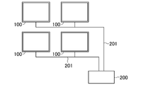
- FIG. 1 is a schematic image diagram of a multi-display system 10.
- the multi-display system 10 is used, for example, for digital signage applications that display a large screen.
- the multi-display system 10 includes a plurality of display devices 100 (four in FIG. 1) and a management unit 200.
- the management unit 200 communicates with each of the display devices 100 via the network 201.
- the management unit 200 has a function of transmitting content to be displayed on each display device 100 and switching display modes in the display device 100.
- Each display device 100 may be connected in parallel as shown in FIG. 1, or may be connected in series by a GPIB interface board (GeneralurPurpose Interface Bus interface board) or the like.
- GPIB interface board GeneralurPurpose Interface Bus interface board
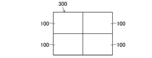
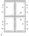
- FIG. 2 shows a state where a plurality of display devices 100 are assembled together.
- a plurality of display devices 100 constitute a large screen display 300 as a whole.
- Each display device 100 may display an enlarged part of the image based on an instruction from the management unit 200 so that one image is formed on the large screen display 300. Further, the same image may be displayed on each display device 100 without being enlarged (that is, four images are displayed in a tile shape). Alternatively, different images may be displayed on each display device 100.
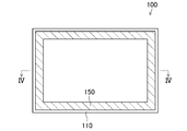
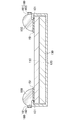
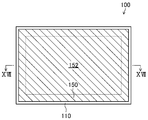
- Display device 3 and 4 are a schematic plan view and a cross-sectional view of the display device 100, respectively.
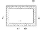
- the display device 100 includes a display panel 110 that performs image display, a backlight unit 120 that causes light to enter the display panel 110, a housing 130 that includes the display panel 110 and the backlight unit 120, and a peripheral portion of the display panel 110.
- the light guide member 150 provided correspondingly is provided. In FIG. 3, the region of the light guide member 150 is indicated by oblique lines.
- the display panel 110 is not shown, two substrates are arranged to face each other, and a sealing material is provided in a frame shape at the peripheral portion between them. Then, a liquid crystal layer is provided in a region surrounded by the sealing material between the substrates, and constitutes a liquid crystal display panel as a whole. A polarizing plate is provided on the surface of each of the two substrates opposite to the liquid crystal layer.
- the display panel 110 is, for example, a 60-inch display having a vertical length of 747 mm and a horizontal length of 1328 mm.
- the backlight unit 120 is disposed so as to face the surface opposite to the display viewing side of the display panel 110.
- the backlight unit 120 includes a light source such as a cold cathode tube or an LED (Light Emitting Diode), and a light guide plate and a diffusion plate that guide light from the light source to the display panel 110.
- a light source such as a cold cathode tube or an LED (Light Emitting Diode)
- a light guide plate and a diffusion plate that guide light from the light source to the display panel 110.
- the housing 130 includes, for example, a front housing portion that includes the display panel 110 and a rear housing portion that supports the backlight unit 120.
- the surface of the housing 130 on the display viewing side is a window frame portion 130F corresponding to the peripheral portion of the display panel 110, and a portion surrounded by the window frame portion 130F constitutes a window portion 130W.
- the display panel 110 is positioned in the housing 130 so that the display image can be visually recognized from the outside through the window portion 130W.
- a spacer 131 is formed in a frame shape along the peripheral edge on the display viewing side surface of the display panel 110, and the display panel 110 and the inner surface of the housing 130 are fixed to each other.
- the light guide member 150 is provided on the surface on the display viewing side of the display panel 110 in a frame shape at the periphery.
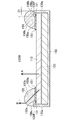
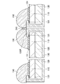
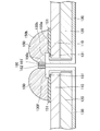
- the light guide member 150 includes a first flat surface 150a that faces the display panel 110, a curved surface 150b that bulges toward the display viewing side, a second flat surface 150c that forms the outer surface of the light guide member 150, Is a plano-convex lens shape.
- the light guide member 150 is formed of, for example, a transparent insulating material such as acrylic resin.
- the light guide member 150 has a width of 10 to 100 mm and a thickness of 10 to 30 mm.
- the light guide member 150 is bonded to the surface of the display panel 110 with an adhesive 151 such as an ultraviolet curable resin or a thermosetting resin on the first flat surface 150a.
- the outer side surface 150 c of the light guide member 150 is positioned closer to the inner peripheral side than the outer side surface 130 a of the housing 130.
- a distance D1 between the outer surface 150c of the light guide member 150 and the outer surface 130a of the housing 130 is, for example, about 0.2 to 0.5 mm.
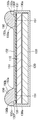
- the light guide member 150 In the area where the light guide member 150 is not provided, the light for displaying an image on the display panel 110 is emitted vertically on the average with respect to the display panel 110 as indicated by an arrow A in FIG.
- the light guide member 150 is provided in a frame shape at the peripheral portion on the display viewing side of the display panel 110, so that light at the peripheral portion of the display panel 110 is guided by the light guide member 150 as indicated by an arrow B in FIG. 4. The light is refracted on the curved surface of the light guide member 150 and travels outward from the display panel 110.
- the multi-display system 10 having the large screen display 300 is configured using a plurality of display devices 100 and an image is enlarged and displayed, the peripheral light out of the image display light is guided to the outside of the display panel 110.
- the display at the joint of each display device 100 is less visible.
- the display device 100 can be manufactured using a conventionally known method or the like.
- the four display devices 100 are arranged in a matrix of 2 rows and 2 columns.
- Each light guide member 150 is positioned in parallel at a boundary portion between adjacent display devices 100, and a buffer material 310 is interposed between the light guide members 150.
- the buffer material 310 is provided so as to extend along the light guide member 150.
- the buffer material 310 is provided so as to contact the outer side surface 150c of the light guide member 150 and the surface 130b of the window frame portion 130F.
- the distance D2 between the adjacent light guide members 150 is, for example, about 0.6 to 1.5 mm.
- the buffer material 310 is formed of a material softer than the acrylic resin that forms the light guide member 150.
- the buffer material 310 is made of a transparent elastic material.
- the buffer material 310 preferably has adhesiveness, whereby the light guide members 150 of the adjacent display devices 100 can be bonded to each other.
- the buffer material 310 is preferably a material having the same refractive index as that of the light guide member 150 or a material having a small difference, for example, about 1.5.
- an acrylic gel sheet, a urethane gel sheet, or the like is suitable as the transparent elastic material forming such a buffer material 310.
- the acrylic gel sheet is a sheet formed from an acrylic gel that has been gelled with a polyacrylic acid ester as a main component.
- the acrylic gel sheet for example, “300Z” series manufactured by Kyori Giken Chemical Co., Ltd. can be suitably used.
- the urethane gel sheet is obtained by forming gel-like polyurethane into a sheet.
- As the urethane gel sheet for example, “SAB (thick film adhesive sheet)” manufactured by Toray Film Processing Co., Ltd. can be suitably used.
- As a material of the buffer material 310 an acrylic gel sheet or a urethane gel sheet, silicone rubber, silicone gel sheet, styrene gel sheet, or the like can be used.
- a method for assembling the large screen display 300 will be described with reference to FIG.
- the four display devices 100 are referred to as display devices 100A, 100B, 100C, and 100D, respectively.
- a buffer material 310a is attached in an L shape along two adjacent sides of the first display device 100A. Then, the display devices 100B and 100C are arranged adjacent to each side so as to sandwich the buffer material 310a. Further, the buffer material 310b is attached to the side of the display device 100B on the side where the display device 110D is arranged, and the buffer material 310c is attached to the side of the display device 100C on the side of the display device 110D where the buffer material 310b, 310c is attached. The last display device 100D is arranged so as to sandwich the.
- a large screen display 300 is configured by fixing these display devices 100A, 100B, 100C, and 100D with external fixing means.
- the buffer material 310 is interposed along the light guide member 150 between the light guide members 150 in the two adjacent display devices 100, a plurality of displays Even if the devices 100 are arranged in a matrix, the light guide members 150 of the adjacent display devices 100 do not directly contact each other. That is, even if the two light guide members 150 are arranged adjacent to each other, the shock absorbing material 310 interposed between the light guide members 150 absorbs the impact, so that the light guide member 150, the bonded portion of the light guide member 150, and the like Thus, the light guide member 150 is prevented from being peeled off or the display panel 110 is damaged.
- the outer surface 150c of the light guide member 150 is positioned closer to the inner peripheral edge than the outer surface 130a of the housing 130.
- the outer surface 150c of the housing 130 may be positioned on the outer peripheral side of the outer surface 130a of the housing 130.
- the frame area of the display panel 110 is different depending on each side of the display panel 110, as shown in FIG. 9 as a second modification, the area having a large frame area (the right side of the left display panel 110 in FIG. 9).
- the outer surface 150c of the light guide member 150 is positioned closer to the inner peripheral side than the outer surface 130a of the housing 130, while the frame region is smaller (in FIG. 9, the left and left sides of the right display panel 110).
- the outer surface 150 c of the light guide member 150 may be positioned on the outer peripheral side of the outer surface 130 a of the housing 130.
- the light guide member 150 includes a first flat surface 150 a that faces the display panel 110, a curved surface 150 b that bulges toward the display viewing side, and a second surface that forms the outer surface of the light guide member 150.
- the light guide member 150 has a flat surface 150a facing the display panel 110 and a curved surface 150b bulging toward the display viewing side (that is, The outer surface of the light guide member 150 is not a flat surface but a part of the curved surface 150b).
- the outer surface of the light guide member 150 is a flat surface from the viewpoint that adjacent display devices 100 are arranged in a matrix without a gap.
- the light guide member 150 is described as being provided with a frame shape covering the outer peripheral edge of the display panel surface.
- the light guide member 150 is the display device 100 of the outer peripheral edge of the display panel 110. May be provided in a region adjacent to the other display device 100 when a plurality of are combined to form the large screen display 300.
- the multi-display system 10 includes a plurality of display devices 100 and a management unit 200, and the large-screen display 300 is configured by combining the plurality of display devices 100 in a matrix.
- Display device 10 and 11 are a schematic plan view and a cross-sectional view of the display device 100, respectively.
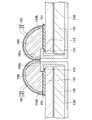
- the display device 100 corresponds to a display panel 110 that performs image display, a backlight unit 120 that causes light to enter the display panel 110, a housing 130 that includes the display panel 110 and the backlight unit 120, and a peripheral portion of the display panel 110. And a buffer material 160 that covers the outer surface of the light guide member 150.
- the buffer material 160 has a configuration in which a buffer material body 161 on the light guide member 150 side and a non-adhesive film 162 covering the surface thereof are laminated.
- the buffer material 160 is provided so as to cover the second flat surface 150 c that is the outer surface of the light guide member 150 and to extend annularly along the light guide member 150.
- the buffer material 160 is provided so as to contact the surface 130 b of the window frame portion 130 ⁇ / b> F of the housing 130. Since the surface of the buffer material main body 161 is covered with the non-adhesive film 162, it is possible to prevent other materials from adhering to the buffer material 160.
- the buffer material main body 161 has adhesiveness and is made of a softer material than the acrylic resin that forms the light guide member 150. Moreover, the buffer material main body 161 is formed of a transparent elastic material. The buffer material main body 161 is preferably made of a material having the same refractive index as that of the light guide member 150 or a small difference, for example, about 1.5.
- An acrylic gel sheet, a urethane gel sheet, or the like is suitable as the transparent elastic material that forms such a buffer material body 161.
- the acrylic gel sheet is a sheet formed from an acrylic gel that has been gelled with a polyacrylic acid ester as a main component. As the acrylic gel sheet, for example, “300Z” series manufactured by Kyori Giken Chemical Co., Ltd. can be suitably used.
- the urethane gel sheet is obtained by forming gel-like polyurethane into a sheet.
- the urethane gel sheet for example, “SAB (thick film adhesive sheet)” manufactured by Toray Film Processing Co., Ltd. can be suitably used.
- As a material of the buffer material main body 161 in addition to an acrylic gel sheet and a urethane gel sheet, silicone rubber, a silicone gel sheet, a styrene gel sheet, and the like can be used.
- the buffer material main body 161 has a thickness of 300 to 700 ⁇ m, for example.
- non-adhesive film 162 examples include a polyethylene terephthalate (PET) film, a triacetyl cellulose (TAC) film, an acrylic film, and a polycarbonate film.
- PET polyethylene terephthalate
- TAC triacetyl cellulose
- acrylic film an acrylic film
- polycarbonate film a polycarbonate film.
- the non-adhesive film 162 has a thickness of 50 to 100 ⁇ m, for example.
- the configuration is the same as that of the first embodiment.
- the display device 100 can be manufactured by attaching the buffer material 160 to the outer side surface 150c of the light guide member 150 of the display device manufactured using a conventionally known method or the like.
- the buffer material 160 may be attached to the outer surface 150c of the light guide member 150 before the light guide member 150 is attached to the display panel 110, and the light guide member 150 is attached to the display panel 110 after the light guide member 150 is attached to the display panel 110.
- the cushioning material 160 may be affixed to the outer side surface 150 c of 150.
- the large-screen display 300 is configured by arranging the display devices 100 having the above-described configuration in a matrix and fixing them with external fixing means.
- each buffer material 160 is interposed between two light guide members positioned in parallel at the boundary portion between adjacent display devices 100.
- the non-adhesive films 162 abut against each other in the cushioning material 160 of the two adjacent display devices 100.
- the buffer material 160 is interposed along the light guide member 150 between the light guide members 150 at the boundary portion between the two adjacent display devices 100. Therefore, even if the plurality of display devices 100 are arranged in a matrix, the light guide members 150 of the adjacent display devices 100 are not in direct contact with each other. That is, even if the two light guide members 150 are disposed adjacent to each other, the shock absorber main body 161 of each of the two shock absorbers 160 interposed between the light guide members 150 absorbs the impact, and thus the light guide member 150. In addition, it is possible to prevent the light guide member 150 from being peeled off or the display panel 110 from being damaged due to the force applied to the bonded portion of the light guide member 150 or the like.
- the large-screen display of the multi-display system 10 can be easily obtained by combining the display devices 100.
- 300 can be configured. Further, in the cushioning material 160 of the display device 100, since the surface of the cushioning material main body 161 is covered with the non-adhesive film 162, the cushioning materials 160 of the adjacent display devices 100 are not bonded to each other and are assembled once. The display 300 can be disassembled again to easily make the individual display devices 100.
- Modification of Embodiment 2 Although the second embodiment has been described on the assumption that the cushioning material 160 is provided so as to cover the second flat surface 150c, the entire surface of the curved surface 150b of the light guide member 150 is further covered as illustrated in FIG. 15 may be provided so as to cover a part of the curved surface 150b of the light guide member 150 and the second flat surface 150c, as shown as Modification 4 in FIG.
- the buffer material 160 As in the modified examples 2 and 3, the light refraction at the interface of the light guide member 150 becomes uniform in the buffer material 160, and more excellent visibility is obtained.
- the buffer material 160 is provided so as to cover the entire surface of the light guide member 150 as in Modification 2, the region where the buffer material is present on the display viewing side of the light guide member 150 and the region where the buffer material is not present There is no break between and better visibility is obtained.
- the multi-display system 10 includes a plurality of display devices 100 and a management unit 200, and the large-screen display 300 is configured by combining the plurality of display devices 100 in a matrix.
- Display device 16 and 17 are a schematic plan view and a cross-sectional view of the display device 100, respectively.
- the display device 100 corresponds to a display panel 110 that performs image display, a backlight unit 120 that causes light to enter the display panel 110, a housing 130 that includes the display panel 110 and the backlight unit 120, and a peripheral portion of the display panel 110. And a front cover 152 that covers the surface of the display panel 110 on the display viewing side.
- the front surface covering portion 152 is integrated with the light guide member 150.
- the joint portion between the light guide member 150 and the front cover portion 152 is connected with a smooth curve in cross section.
- the curved surface 150b bulging to the display viewing side of the light guide member 150 and the surface 152a on the display viewing side of the front cover 152 are connected by a smooth curved surface 150d as shown in an enlarged view in FIG. ing.
- the front cover 152 has a thickness of 0.5 to 5 mm, for example.
- the light guide member 150 and the front cover portion 152 are integrally molded so as to have the shape described above, and then adhered to the surface of the display panel 110 with an adhesive 151.
- the configuration is the same as that of the first embodiment.
- the buffer material 310 is interposed along the light guide member 150 between the light guide members 150 in the two adjacent display devices 100, a plurality of displays Even if the devices 100 are arranged in a matrix, the light guide members 150 of the adjacent display devices 100 do not directly contact each other. That is, even if the two light guide members 150 are arranged adjacent to each other, the shock absorbing material 310 interposed between the light guide members 150 absorbs the impact, so that the light guide member 150, the bonded portion of the light guide member 150, and the like Thus, the light guide member 150 is prevented from being peeled off or the display panel 110 is damaged.
- the front cover 152 that is integrated with the light guide member 150 is provided, the curved surface 150b that bulges toward the display viewing side of the light guide member 150, and the front cover. Since the surface 152a on the display viewing side of the portion 152 is connected by a smooth curved surface 150d, the light emitted from the curved surface 150b through the light guide member 150 and the surface 152a emitted from the inside of the light guide member 150 are emitted from the surface 152a. There is no boundary line at the joint with the emitted light. Therefore, a more natural display for the viewer is visually recognized.
- the display device 100 of the present embodiment since the surface of the display panel 110 is covered with the front cover portion 152, the physical strength of the display panel 110 is increased.
- the display device 100 has been described as related to a liquid crystal display device.
- the display device 100 is not limited to this.
- an organic EL display device an inorganic EL display device, an electrophoretic display device, (Plasma display)), plasma addressed liquid crystal display (PALC), field emission display (FED) or surface-conduction electron-emitter display (SED) Etc.
- the display panel 110 may be driven by a field sequential color system.
- the present invention is useful for a display device and a multi-display system that displays a seamless image using the display device.
Landscapes
- Physics & Mathematics (AREA)
- Engineering & Computer Science (AREA)
- Nonlinear Science (AREA)
- General Engineering & Computer Science (AREA)
- Optics & Photonics (AREA)
- General Physics & Mathematics (AREA)
- Crystallography & Structural Chemistry (AREA)
- Chemical & Material Sciences (AREA)
- Multimedia (AREA)
- Signal Processing (AREA)
- Mathematical Physics (AREA)
- Devices For Indicating Variable Information By Combining Individual Elements (AREA)
- Liquid Crystal (AREA)
Abstract
L'objectif de la présente invention est d'empêcher un élément de guidage de lumière de s'arracher à la suite d'une contrainte appliquée à l'élément de guidage de lumière ou à la section adhésive de l'élément de guidage de lumière et d'empêcher un panneau d'affichage de se détériorer. Dans un système multi-affichages, une pluralité de dispositifs d'affichage (100) est disposée sous la forme d'une matrice de sorte qu'un matériau amortisseur de chocs (310) soit disposé entre et le long des éléments de guidage de lumière (150) sur deux dispositifs d'affichage adjacents (100) de la pluralité de dispositifs d'affichage (100).
Priority Applications (1)
| Application Number | Priority Date | Filing Date | Title |
|---|---|---|---|
| US14/117,605 US9140433B2 (en) | 2011-05-16 | 2012-05-09 | Multi display system, and display device |
Applications Claiming Priority (2)
| Application Number | Priority Date | Filing Date | Title |
|---|---|---|---|
| JP2011-109189 | 2011-05-16 | ||
| JP2011109189 | 2011-05-16 |
Publications (1)
| Publication Number | Publication Date |
|---|---|
| WO2012157207A1 true WO2012157207A1 (fr) | 2012-11-22 |
Family
ID=47176559
Family Applications (1)
| Application Number | Title | Priority Date | Filing Date |
|---|---|---|---|
| PCT/JP2012/003025 Ceased WO2012157207A1 (fr) | 2011-05-16 | 2012-05-09 | Système multi-affichages et dispositif d'affichage |
Country Status (2)
| Country | Link |
|---|---|
| US (1) | US9140433B2 (fr) |
| WO (1) | WO2012157207A1 (fr) |
Cited By (4)
| Publication number | Priority date | Publication date | Assignee | Title |
|---|---|---|---|---|
| KR20150008666A (ko) * | 2013-07-15 | 2015-01-23 | 엘지전자 주식회사 | 멀티비전 디바이스 및 이에 부착되는 렌즈 바 |
| KR20150060070A (ko) * | 2013-11-25 | 2015-06-03 | 엘지디스플레이 주식회사 | 멀티 비전 디스플레이 장치 |
| WO2016063343A1 (fr) * | 2014-10-21 | 2016-04-28 | 三菱電機株式会社 | Couvercle de dispositif d'affichage de véhicule et dispositif d'affichage de véhicule |
| CN107037966A (zh) * | 2015-09-09 | 2017-08-11 | 三星电子株式会社 | 感测输入的压力的电子设备和用于操作电子设备的方法 |
Families Citing this family (7)
| Publication number | Priority date | Publication date | Assignee | Title |
|---|---|---|---|---|
| CN104503115B (zh) * | 2015-01-14 | 2017-12-05 | 合肥鑫晟光电科技有限公司 | 一种显示面板和显示装置 |
| US10191187B2 (en) * | 2015-03-31 | 2019-01-29 | Samsung Electronics Co., Ltd. | Outdoor display apparatus |
| US10628111B2 (en) * | 2016-11-08 | 2020-04-21 | Frank Michael Weyer | Method and apparatus for optically concealing video wall seams |
| KR102740814B1 (ko) * | 2016-12-20 | 2024-12-09 | 엘지디스플레이 주식회사 | 표시 장치와 이를 포함하는 멀티 스크린 표시 장치 |
| WO2019187735A1 (fr) * | 2018-03-29 | 2019-10-03 | ソニー株式会社 | Dispositif d'affichage |
| CN108957818A (zh) * | 2018-06-29 | 2018-12-07 | 苏州佳世达电通有限公司 | 显示模组、显示装置以及显示器 |
| US11275403B2 (en) | 2019-03-08 | 2022-03-15 | Innolux Corporation | Tiled display device |
Citations (4)
| Publication number | Priority date | Publication date | Assignee | Title |
|---|---|---|---|---|
| JPS59216186A (ja) * | 1983-05-23 | 1984-12-06 | 三菱電機株式会社 | 表示装置 |
| JPH043089A (ja) * | 1990-04-20 | 1992-01-08 | Fujitsu General Ltd | 表示装置およびその製造方法 |
| WO2008149449A1 (fr) * | 2007-06-07 | 2008-12-11 | Telesystems Co., Ltd. | Dispositif à multiples affichages |
| WO2010092794A1 (fr) * | 2009-02-10 | 2010-08-19 | シャープ株式会社 | Dispositif d'affichage et procédé de fabrication associé |
Family Cites Families (11)
| Publication number | Priority date | Publication date | Assignee | Title |
|---|---|---|---|---|
| CA2084103C (fr) * | 1991-12-02 | 1999-07-27 | Keiji Sakai | Un affichage |
| US5867236A (en) * | 1996-05-21 | 1999-02-02 | Rainbow Displays, Inc. | Construction and sealing of tiled, flat-panel displays |
| US6897855B1 (en) * | 1998-02-17 | 2005-05-24 | Sarnoff Corporation | Tiled electronic display structure |
| JP2004510186A (ja) * | 2000-09-19 | 2004-04-02 | キム、シハン | マルチディスプレイ装置 |
| GB0028890D0 (en) * | 2000-11-27 | 2001-01-10 | Isis Innovation | Visual display screen arrangement |
| KR101030537B1 (ko) * | 2004-06-30 | 2011-04-21 | 엘지디스플레이 주식회사 | 액정표시장치 및 그를 이용한 휘도 편차 보상방법 |
| US20070058114A1 (en) * | 2005-09-12 | 2007-03-15 | Asahi Glass Company, Limited | Light control device |
| US8089582B2 (en) * | 2007-05-31 | 2012-01-03 | Hitachi Displays, Ltd. | Liquid crystal display device comprising at least one groove having an end portion that stops short of the non-adjacent opposite side surfaces and extends in a direction perpendicular to the non-adjacent side surfaces |
| JP2010072522A (ja) | 2008-09-22 | 2010-04-02 | Nec Personal Products Co Ltd | ディスプレイ装置およびデータ表示方法 |
| JP2010097070A (ja) * | 2008-10-17 | 2010-04-30 | Nitto Denko Corp | フラットパネルディスプレイ用透明粘着シート及びフラットパネルディスプレイ |
| WO2010140537A1 (fr) * | 2009-06-03 | 2010-12-09 | シャープ株式会社 | Dispositif d'affichage |
-
2012
- 2012-05-09 WO PCT/JP2012/003025 patent/WO2012157207A1/fr not_active Ceased
- 2012-05-09 US US14/117,605 patent/US9140433B2/en not_active Expired - Fee Related
Patent Citations (4)
| Publication number | Priority date | Publication date | Assignee | Title |
|---|---|---|---|---|
| JPS59216186A (ja) * | 1983-05-23 | 1984-12-06 | 三菱電機株式会社 | 表示装置 |
| JPH043089A (ja) * | 1990-04-20 | 1992-01-08 | Fujitsu General Ltd | 表示装置およびその製造方法 |
| WO2008149449A1 (fr) * | 2007-06-07 | 2008-12-11 | Telesystems Co., Ltd. | Dispositif à multiples affichages |
| WO2010092794A1 (fr) * | 2009-02-10 | 2010-08-19 | シャープ株式会社 | Dispositif d'affichage et procédé de fabrication associé |
Cited By (8)
| Publication number | Priority date | Publication date | Assignee | Title |
|---|---|---|---|---|
| KR20150008666A (ko) * | 2013-07-15 | 2015-01-23 | 엘지전자 주식회사 | 멀티비전 디바이스 및 이에 부착되는 렌즈 바 |
| KR102034586B1 (ko) * | 2013-07-15 | 2019-10-21 | 엘지전자 주식회사 | 멀티비전 디바이스 및 이에 부착되는 렌즈 바 |
| KR20150060070A (ko) * | 2013-11-25 | 2015-06-03 | 엘지디스플레이 주식회사 | 멀티 비전 디스플레이 장치 |
| KR102009884B1 (ko) * | 2013-11-25 | 2019-10-21 | 엘지디스플레이 주식회사 | 멀티 비전 디스플레이 장치 |
| WO2016063343A1 (fr) * | 2014-10-21 | 2016-04-28 | 三菱電機株式会社 | Couvercle de dispositif d'affichage de véhicule et dispositif d'affichage de véhicule |
| JPWO2016063343A1 (ja) * | 2014-10-21 | 2017-04-27 | 三菱電機株式会社 | 車両用表示器カバー及び車両用表示器 |
| CN107037966A (zh) * | 2015-09-09 | 2017-08-11 | 三星电子株式会社 | 感测输入的压力的电子设备和用于操作电子设备的方法 |
| CN107037966B (zh) * | 2015-09-09 | 2021-10-26 | 三星电子株式会社 | 感测输入的压力的电子设备和用于操作电子设备的方法 |
Also Published As
| Publication number | Publication date |
|---|---|
| US20140218918A1 (en) | 2014-08-07 |
| US9140433B2 (en) | 2015-09-22 |
Similar Documents
| Publication | Publication Date | Title |
|---|---|---|
| WO2012157207A1 (fr) | Système multi-affichages et dispositif d'affichage | |
| JP6267936B2 (ja) | 曲面ディスプレイ装置 | |
| KR102272216B1 (ko) | 타일드 표시 장치 | |
| JP5694383B2 (ja) | 表示装置 | |
| JP5679604B2 (ja) | 液晶表示装置および液晶表示装置の製造方法 | |
| JP4731637B2 (ja) | 表示装置 | |
| US8797234B2 (en) | Display device including light-transmitting cover with lens portion and electronic device including same | |
| JP5892736B2 (ja) | 表示装置 | |
| US9709783B2 (en) | Display apparatus having bezel hiding member | |
| TWI402572B (zh) | 背光單元、用於組裝背光單元的方法、及使用該背光單元的液晶顯示裝置 | |
| US9835898B2 (en) | Display unit | |
| US9626053B2 (en) | Touch control display device and joint touch control display | |
| WO2012161260A1 (fr) | Dispositif d'affichage | |
| KR20140139844A (ko) | 멀티 패널 표시 장치 및 그 제조 방법 | |
| TW201513070A (zh) | 顯示裝置及拼接式顯示器 | |
| US9146343B2 (en) | Display device, multi-display system and method for manufacturing display device | |
| CN105723441A (zh) | 显示装置 | |
| CN107390413B (zh) | 拼接式显示装置及其拼接方法 | |
| US20140233261A1 (en) | Display device and multi-display device | |
| WO2012147323A1 (fr) | Procédé de fabrication d'un écran, écran, et système multi-écran | |
| KR102148823B1 (ko) | 멀티 패널 표시 장치 | |
| US20140132848A1 (en) | Illuminating device, display device, and television receiver | |
| KR102372343B1 (ko) | 표시장치 | |
| KR102421867B1 (ko) | 표시장치 | |
| KR102239593B1 (ko) | 표시장치 및 그를 포함하는 세트 전자 장치 |
Legal Events
| Date | Code | Title | Description |
|---|---|---|---|
| 121 | Ep: the epo has been informed by wipo that ep was designated in this application |
Ref document number: 12786540 Country of ref document: EP Kind code of ref document: A1 |
|
| WWE | Wipo information: entry into national phase |
Ref document number: 14117605 Country of ref document: US |
|
| NENP | Non-entry into the national phase |
Ref country code: DE |
|
| 122 | Ep: pct application non-entry in european phase |
Ref document number: 12786540 Country of ref document: EP Kind code of ref document: A1 |
|
| NENP | Non-entry into the national phase |
Ref country code: JP |