WO2012160859A1 - Elément électroluminescent organique, dispositif d'affichage et dispositif d'éclairage - Google Patents
Elément électroluminescent organique, dispositif d'affichage et dispositif d'éclairage Download PDFInfo
- Publication number
- WO2012160859A1 WO2012160859A1 PCT/JP2012/056229 JP2012056229W WO2012160859A1 WO 2012160859 A1 WO2012160859 A1 WO 2012160859A1 JP 2012056229 W JP2012056229 W JP 2012056229W WO 2012160859 A1 WO2012160859 A1 WO 2012160859A1
- Authority
- WO
- WIPO (PCT)
- Prior art keywords
- group
- light emitting
- emitting layer
- organic
- ring
- Prior art date
- Legal status (The legal status is an assumption and is not a legal conclusion. Google has not performed a legal analysis and makes no representation as to the accuracy of the status listed.)
- Ceased
Links
- 0 CC*(C)c1ccccc1C(*(*)C=C1)=*1*(cccc1)c1C(OC)=O Chemical compound CC*(C)c1ccccc1C(*(*)C=C1)=*1*(cccc1)c1C(OC)=O 0.000 description 6
- JLLXCMXFAWTPMD-UHFFFAOYSA-N c(cc1)ccc1-c(cc1c2ccccc22)ccc1[n]2-c1cc(-c(cc2c3ccccc33)ccc2[n]3-c2ccccc2)ccc1 Chemical compound c(cc1)ccc1-c(cc1c2ccccc22)ccc1[n]2-c1cc(-c(cc2c3ccccc33)ccc2[n]3-c2ccccc2)ccc1 JLLXCMXFAWTPMD-UHFFFAOYSA-N 0.000 description 2
- OHFPUYXMACOCBL-UHFFFAOYSA-N C(C1c2c3cccc2)=CC=CC1N3c1cc(N(C2C=CC=CC22)c3c2cccc3)cc(-c2cc(-[n]3c4ccccc4c4c3cccc4)cc(-[n]3c4ccccc4c4c3cccc4)c2)c1 Chemical compound C(C1c2c3cccc2)=CC=CC1N3c1cc(N(C2C=CC=CC22)c3c2cccc3)cc(-c2cc(-[n]3c4ccccc4c4c3cccc4)cc(-[n]3c4ccccc4c4c3cccc4)c2)c1 OHFPUYXMACOCBL-UHFFFAOYSA-N 0.000 description 1
- QFRMDBNFYQPWGQ-UHFFFAOYSA-N C(C1c2ccccc22)=CC=CC1N2c(cc1)ccc1-c1cc(N(C2C=CC=CC22)c3c2cccc3)cc(N2c3ccccc3C3C=CC=CC23)c1 Chemical compound C(C1c2ccccc22)=CC=CC1N2c(cc1)ccc1-c1cc(N(C2C=CC=CC22)c3c2cccc3)cc(N2c3ccccc3C3C=CC=CC23)c1 QFRMDBNFYQPWGQ-UHFFFAOYSA-N 0.000 description 1
- SCAPBYFBZXXUQT-UHFFFAOYSA-N C(C1c2ccccc22)=CC=CC1N2c1cc(-c2cccc(-[n]3c4ccccc4c4c3cccc4)c2)ccc1 Chemical compound C(C1c2ccccc22)=CC=CC1N2c1cc(-c2cccc(-[n]3c4ccccc4c4c3cccc4)c2)ccc1 SCAPBYFBZXXUQT-UHFFFAOYSA-N 0.000 description 1
- XWSXKPBVUOWVMJ-UHFFFAOYSA-O Cc(cc1C)cc(c2cccc(C(C3)[IH]3(C)c3c(c4ncc[n]4c4c5cc(C=C)cc4C)c5ccc3)c22)c1[n]1c2[nH+]cc1 Chemical compound Cc(cc1C)cc(c2cccc(C(C3)[IH]3(C)c3c(c4ncc[n]4c4c5cc(C=C)cc4C)c5ccc3)c22)c1[n]1c2[nH+]cc1 XWSXKPBVUOWVMJ-UHFFFAOYSA-O 0.000 description 1
- CBNWNTUTZGAZTF-UHFFFAOYSA-N c(cc1)cc(c2c3)c1[o]c2ccc3-c(cc1)cc(c2cc(-c3ccc4[o]c(cccc5)c5c4c3)ccc22)c1[n]2-c1cc(-[n]2c(ccc(-c(cc3)cc4c3[o]c3ccccc43)c3)c3c3cc(-c(cc4)cc5c4[o]c4ccccc54)ccc23)ccc1 Chemical compound c(cc1)cc(c2c3)c1[o]c2ccc3-c(cc1)cc(c2cc(-c3ccc4[o]c(cccc5)c5c4c3)ccc22)c1[n]2-c1cc(-[n]2c(ccc(-c(cc3)cc4c3[o]c3ccccc43)c3)c3c3cc(-c(cc4)cc5c4[o]c4ccccc54)ccc23)ccc1 CBNWNTUTZGAZTF-UHFFFAOYSA-N 0.000 description 1
- AWXGSYPUMWKTBR-UHFFFAOYSA-N c(cc1)cc(c2c3cccc2)c1[n]3-c(cc1)ccc1N(c(cc1)ccc1-[n]1c(cccc2)c2c2c1cccc2)c(cc1)ccc1-[n]1c2ccccc2c2c1cccc2 Chemical compound c(cc1)cc(c2c3cccc2)c1[n]3-c(cc1)ccc1N(c(cc1)ccc1-[n]1c(cccc2)c2c2c1cccc2)c(cc1)ccc1-[n]1c2ccccc2c2c1cccc2 AWXGSYPUMWKTBR-UHFFFAOYSA-N 0.000 description 1
- YCCGKMOVAKCKDM-UHFFFAOYSA-N c(cc1)cc(c2c3cccc2)c1[n]3-c1cc(-[n]2c3ccccc3c3c2cccc3)cc(-c(cc2)cc3c2[o]c2ccccc32)c1 Chemical compound c(cc1)cc(c2c3cccc2)c1[n]3-c1cc(-[n]2c3ccccc3c3c2cccc3)cc(-c(cc2)cc3c2[o]c2ccccc32)c1 YCCGKMOVAKCKDM-UHFFFAOYSA-N 0.000 description 1
- KBIRSRDVZYSTJU-UHFFFAOYSA-N c(cc1)cc(c2cc(-c3cc(-c(cc4)cc(c5ccccc55)c4[n]5-c(cc4)cc5c4[o]c4c5cccc4)ccc3)ccc22)c1[n]2-c(cc1)cc2c1[o]c1ccccc21 Chemical compound c(cc1)cc(c2cc(-c3cc(-c(cc4)cc(c5ccccc55)c4[n]5-c(cc4)cc5c4[o]c4c5cccc4)ccc3)ccc22)c1[n]2-c(cc1)cc2c1[o]c1ccccc21 KBIRSRDVZYSTJU-UHFFFAOYSA-N 0.000 description 1
- ZGEUUNNIQMDTKF-UHFFFAOYSA-N c(cc1)cc(c2ccccc22)c1[n]2-c(cc1)cc(c2c3)c1[o]c2ccc3-c1cccc(-c2ccc3[o]c(ccc(-[n]4c(cccc5)c5c5c4cccc5)c4)c4c3c2)c1 Chemical compound c(cc1)cc(c2ccccc22)c1[n]2-c(cc1)cc(c2c3)c1[o]c2ccc3-c1cccc(-c2ccc3[o]c(ccc(-[n]4c(cccc5)c5c5c4cccc5)c4)c4c3c2)c1 ZGEUUNNIQMDTKF-UHFFFAOYSA-N 0.000 description 1
- VFUDMQLBKNMONU-UHFFFAOYSA-N c(cc1)cc(c2ccccc22)c1[n]2-c(cc1)ccc1-c(cc1)ccc1-[n]1c(cccc2)c2c2c1cccc2 Chemical compound c(cc1)cc(c2ccccc22)c1[n]2-c(cc1)ccc1-c(cc1)ccc1-[n]1c(cccc2)c2c2c1cccc2 VFUDMQLBKNMONU-UHFFFAOYSA-N 0.000 description 1
- MZYDBGLUVPLRKR-UHFFFAOYSA-N c(cc1)cc(c2ccccc22)c1[n]2-c1cc(-[n]2c(cccc3)c3c3c2cccc3)ccc1 Chemical compound c(cc1)cc(c2ccccc22)c1[n]2-c1cc(-[n]2c(cccc3)c3c3c2cccc3)ccc1 MZYDBGLUVPLRKR-UHFFFAOYSA-N 0.000 description 1
- ZMJOWHNGBSQMJG-UHFFFAOYSA-N c(cc1)ccc1-[n](c(cccc1)c1c1c2)c1ccc2-c(cc1)cc(c2c3cccc2)c1[n]3-c1cc(-[n](c2ccccc2c2c3)c2ccc3-c(cc2)cc(c3ccccc33)c2[n]3-c2ccccc2)ccc1 Chemical compound c(cc1)ccc1-[n](c(cccc1)c1c1c2)c1ccc2-c(cc1)cc(c2c3cccc2)c1[n]3-c1cc(-[n](c2ccccc2c2c3)c2ccc3-c(cc2)cc(c3ccccc33)c2[n]3-c2ccccc2)ccc1 ZMJOWHNGBSQMJG-UHFFFAOYSA-N 0.000 description 1
- ILDUFPWBKKKNIW-UHFFFAOYSA-N c(cc1)ccc1-[n](c(cccc1)c1c1c2)c1ccc2-c1cc(-[n]2c(ccc(-c(cc3)cc4c3[o]c3c4cccc3)c3)c3c3c2cccc3)ccc1 Chemical compound c(cc1)ccc1-[n](c(cccc1)c1c1c2)c1ccc2-c1cc(-[n]2c(ccc(-c(cc3)cc4c3[o]c3c4cccc3)c3)c3c3c2cccc3)ccc1 ILDUFPWBKKKNIW-UHFFFAOYSA-N 0.000 description 1
- ZYXQUIQJNOGTGL-UHFFFAOYSA-N c(cc1)ccc1-[n](c(cccc1)c1c1c2)c1ccc2-c1cc(-[n]2c3ccccc3c3ccccc23)cc(-c(cc2)cc(c3ccccc33)c2[n]3-c2ccccc2)c1 Chemical compound c(cc1)ccc1-[n](c(cccc1)c1c1c2)c1ccc2-c1cc(-[n]2c3ccccc3c3ccccc23)cc(-c(cc2)cc(c3ccccc33)c2[n]3-c2ccccc2)c1 ZYXQUIQJNOGTGL-UHFFFAOYSA-N 0.000 description 1
- WWFRJQCFBCQJCU-UHFFFAOYSA-N c(cc1)ccc1-[n](c(cccc1)c1c1c2)c1ccc2-c1cc(-c(cc2)cc3c2[o]c2ccccc32)ccc1 Chemical compound c(cc1)ccc1-[n](c(cccc1)c1c1c2)c1ccc2-c1cc(-c(cc2)cc3c2[o]c2ccccc32)ccc1 WWFRJQCFBCQJCU-UHFFFAOYSA-N 0.000 description 1
- ZMBMXPKEHHFHEM-UHFFFAOYSA-N c(cc1)ccc1-[n]1c(cc(cc2)-c3ccc4[o]c(ccc(-c(cc5)cc6c5c(cccc5)c5[n]6-c5ccccc5)c5)c5c4c3)c2c2c1cccc2 Chemical compound c(cc1)ccc1-[n]1c(cc(cc2)-c3ccc4[o]c(ccc(-c(cc5)cc6c5c(cccc5)c5[n]6-c5ccccc5)c5)c5c4c3)c2c2c1cccc2 ZMBMXPKEHHFHEM-UHFFFAOYSA-N 0.000 description 1
- ZEGYQBGJQMTXKA-UHFFFAOYSA-N c(cc1)ccc1-[n]1c(ccc(-[n]2c3ccccc3c3ccccc23)c2)c2c2cc(-[n]3c4ccccc4c4c3cccc4)ccc12 Chemical compound c(cc1)ccc1-[n]1c(ccc(-[n]2c3ccccc3c3ccccc23)c2)c2c2cc(-[n]3c4ccccc4c4c3cccc4)ccc12 ZEGYQBGJQMTXKA-UHFFFAOYSA-N 0.000 description 1
- NGPVTXZPZDYWNO-UHFFFAOYSA-N c(cc1)ccc1-[n]1c(ccc(-c2cccc(-[n]3c4ccccc4c4c3cccc4)c2)c2)c2c2c1cccc2 Chemical compound c(cc1)ccc1-[n]1c(ccc(-c2cccc(-[n]3c4ccccc4c4c3cccc4)c2)c2)c2c2c1cccc2 NGPVTXZPZDYWNO-UHFFFAOYSA-N 0.000 description 1
- MQFCCSXRKNAXFS-UHFFFAOYSA-N c(cc1)ccc1-[n]1c(ccc(-c2cccc(-c(cc3c4c5cccc4)ccc3[n]5-c3ccccc3)c2)c2)c2c2ccccc12 Chemical compound c(cc1)ccc1-[n]1c(ccc(-c2cccc(-c(cc3c4c5cccc4)ccc3[n]5-c3ccccc3)c2)c2)c2c2ccccc12 MQFCCSXRKNAXFS-UHFFFAOYSA-N 0.000 description 1
- TYACDNYYXBXTMX-UHFFFAOYSA-N c(cc1)ccc1-c(cc1c2c3)ccc1[o]c2ccc3-c1cc(-[n]2c3ccccc3c3c2cccc3)cc(-[n]2c(cccc3)c3c3c2cccc3)c1 Chemical compound c(cc1)ccc1-c(cc1c2c3)ccc1[o]c2ccc3-c1cc(-[n]2c3ccccc3c3c2cccc3)cc(-[n]2c(cccc3)c3c3c2cccc3)c1 TYACDNYYXBXTMX-UHFFFAOYSA-N 0.000 description 1
- RUQBUIPCKJWQNW-UHFFFAOYSA-N c(cc1)ccc1[Si](c(c(-c1c2)c3)ccc3-[n]3c(cccc4)c4c4c3cccc4)(c1ccc2-[n]1c2ccccc2c2c1cccc2)c1ccccc1 Chemical compound c(cc1)ccc1[Si](c(c(-c1c2)c3)ccc3-[n]3c(cccc4)c4c4c3cccc4)(c1ccc2-[n]1c2ccccc2c2c1cccc2)c1ccccc1 RUQBUIPCKJWQNW-UHFFFAOYSA-N 0.000 description 1
- NYBJAOSPRUREKJ-UHFFFAOYSA-N c(cc1c2c3ccc(-c4ccc5[o]c(cccc6)c6c5c4)c2)ccc1[n]3-c1cc(-[n](c(cccc2)c2c2c3)c2ccc3-c(cc2)cc3c2[o]c2ccccc32)ccc1 Chemical compound c(cc1c2c3ccc(-c4ccc5[o]c(cccc6)c6c5c4)c2)ccc1[n]3-c1cc(-[n](c(cccc2)c2c2c3)c2ccc3-c(cc2)cc3c2[o]c2ccccc32)ccc1 NYBJAOSPRUREKJ-UHFFFAOYSA-N 0.000 description 1
- JUOPLIWLGISFCN-UHFFFAOYSA-N c1ccc(C(c(c(-c2c3)c4)ccc4-[n]4c(cccc5)c5c5c4cccc5)(c2ccc3-[n]2c3ccccc3c3c2cccc3)c2ccccc2)cc1 Chemical compound c1ccc(C(c(c(-c2c3)c4)ccc4-[n]4c(cccc5)c5c5c4cccc5)(c2ccc3-[n]2c3ccccc3c3c2cccc3)c2ccccc2)cc1 JUOPLIWLGISFCN-UHFFFAOYSA-N 0.000 description 1
Images

Classifications
-
- C—CHEMISTRY; METALLURGY
- C07—ORGANIC CHEMISTRY
- C07D—HETEROCYCLIC COMPOUNDS
- C07D405/00—Heterocyclic compounds containing both one or more hetero rings having oxygen atoms as the only ring hetero atoms, and one or more rings having nitrogen as the only ring hetero atom
- C07D405/14—Heterocyclic compounds containing both one or more hetero rings having oxygen atoms as the only ring hetero atoms, and one or more rings having nitrogen as the only ring hetero atom containing three or more hetero rings
-
- C—CHEMISTRY; METALLURGY
- C07—ORGANIC CHEMISTRY
- C07D—HETEROCYCLIC COMPOUNDS
- C07D209/00—Heterocyclic compounds containing five-membered rings, condensed with other rings, with one nitrogen atom as the only ring hetero atom
- C07D209/56—Ring systems containing three or more rings
- C07D209/80—[b, c]- or [b, d]-condensed
- C07D209/82—Carbazoles; Hydrogenated carbazoles
- C07D209/86—Carbazoles; Hydrogenated carbazoles with only hydrogen atoms, hydrocarbon or substituted hydrocarbon radicals, directly attached to carbon atoms of the ring system
-
- C—CHEMISTRY; METALLURGY
- C07—ORGANIC CHEMISTRY
- C07D—HETEROCYCLIC COMPOUNDS
- C07D403/00—Heterocyclic compounds containing two or more hetero rings, having nitrogen atoms as the only ring hetero atoms, not provided for by group C07D401/00
- C07D403/14—Heterocyclic compounds containing two or more hetero rings, having nitrogen atoms as the only ring hetero atoms, not provided for by group C07D401/00 containing three or more hetero rings
-
- C—CHEMISTRY; METALLURGY
- C07—ORGANIC CHEMISTRY
- C07D—HETEROCYCLIC COMPOUNDS
- C07D409/00—Heterocyclic compounds containing two or more hetero rings, at least one ring having sulfur atoms as the only ring hetero atoms
- C07D409/14—Heterocyclic compounds containing two or more hetero rings, at least one ring having sulfur atoms as the only ring hetero atoms containing three or more hetero rings
-
- C—CHEMISTRY; METALLURGY
- C07—ORGANIC CHEMISTRY
- C07D—HETEROCYCLIC COMPOUNDS
- C07D471/00—Heterocyclic compounds containing nitrogen atoms as the only ring hetero atoms in the condensed system, at least one ring being a six-membered ring with one nitrogen atom, not provided for by groups C07D451/00 - C07D463/00
- C07D471/12—Heterocyclic compounds containing nitrogen atoms as the only ring hetero atoms in the condensed system, at least one ring being a six-membered ring with one nitrogen atom, not provided for by groups C07D451/00 - C07D463/00 in which the condensed system contains three hetero rings
- C07D471/14—Ortho-condensed systems
-
- C—CHEMISTRY; METALLURGY
- C09—DYES; PAINTS; POLISHES; NATURAL RESINS; ADHESIVES; COMPOSITIONS NOT OTHERWISE PROVIDED FOR; APPLICATIONS OF MATERIALS NOT OTHERWISE PROVIDED FOR
- C09K—MATERIALS FOR MISCELLANEOUS APPLICATIONS, NOT PROVIDED FOR ELSEWHERE
- C09K11/00—Luminescent materials, e.g. electroluminescent or chemiluminescent
- C09K11/06—Luminescent materials, e.g. electroluminescent or chemiluminescent containing organic luminescent materials
-
- H—ELECTRICITY
- H05—ELECTRIC TECHNIQUES NOT OTHERWISE PROVIDED FOR
- H05B—ELECTRIC HEATING; ELECTRIC LIGHT SOURCES NOT OTHERWISE PROVIDED FOR; CIRCUIT ARRANGEMENTS FOR ELECTRIC LIGHT SOURCES, IN GENERAL
- H05B33/00—Electroluminescent light sources
- H05B33/10—Apparatus or processes specially adapted to the manufacture of electroluminescent light sources
-
- H—ELECTRICITY
- H10—SEMICONDUCTOR DEVICES; ELECTRIC SOLID-STATE DEVICES NOT OTHERWISE PROVIDED FOR
- H10K—ORGANIC ELECTRIC SOLID-STATE DEVICES
- H10K50/00—Organic light-emitting devices
- H10K50/10—OLEDs or polymer light-emitting diodes [PLED]
- H10K50/11—OLEDs or polymer light-emitting diodes [PLED] characterised by the electroluminescent [EL] layers
-
- C—CHEMISTRY; METALLURGY
- C09—DYES; PAINTS; POLISHES; NATURAL RESINS; ADHESIVES; COMPOSITIONS NOT OTHERWISE PROVIDED FOR; APPLICATIONS OF MATERIALS NOT OTHERWISE PROVIDED FOR
- C09K—MATERIALS FOR MISCELLANEOUS APPLICATIONS, NOT PROVIDED FOR ELSEWHERE
- C09K2211/00—Chemical nature of organic luminescent or tenebrescent compounds
- C09K2211/10—Non-macromolecular compounds
- C09K2211/1003—Carbocyclic compounds
- C09K2211/1007—Non-condensed systems
-
- C—CHEMISTRY; METALLURGY
- C09—DYES; PAINTS; POLISHES; NATURAL RESINS; ADHESIVES; COMPOSITIONS NOT OTHERWISE PROVIDED FOR; APPLICATIONS OF MATERIALS NOT OTHERWISE PROVIDED FOR
- C09K—MATERIALS FOR MISCELLANEOUS APPLICATIONS, NOT PROVIDED FOR ELSEWHERE
- C09K2211/00—Chemical nature of organic luminescent or tenebrescent compounds
- C09K2211/10—Non-macromolecular compounds
- C09K2211/1003—Carbocyclic compounds
- C09K2211/1011—Condensed systems
-
- C—CHEMISTRY; METALLURGY
- C09—DYES; PAINTS; POLISHES; NATURAL RESINS; ADHESIVES; COMPOSITIONS NOT OTHERWISE PROVIDED FOR; APPLICATIONS OF MATERIALS NOT OTHERWISE PROVIDED FOR
- C09K—MATERIALS FOR MISCELLANEOUS APPLICATIONS, NOT PROVIDED FOR ELSEWHERE
- C09K2211/00—Chemical nature of organic luminescent or tenebrescent compounds
- C09K2211/10—Non-macromolecular compounds
- C09K2211/1018—Heterocyclic compounds
- C09K2211/1025—Heterocyclic compounds characterised by ligands
- C09K2211/1029—Heterocyclic compounds characterised by ligands containing one nitrogen atom as the heteroatom
-
- C—CHEMISTRY; METALLURGY
- C09—DYES; PAINTS; POLISHES; NATURAL RESINS; ADHESIVES; COMPOSITIONS NOT OTHERWISE PROVIDED FOR; APPLICATIONS OF MATERIALS NOT OTHERWISE PROVIDED FOR
- C09K—MATERIALS FOR MISCELLANEOUS APPLICATIONS, NOT PROVIDED FOR ELSEWHERE
- C09K2211/00—Chemical nature of organic luminescent or tenebrescent compounds
- C09K2211/10—Non-macromolecular compounds
- C09K2211/1018—Heterocyclic compounds
- C09K2211/1025—Heterocyclic compounds characterised by ligands
- C09K2211/1088—Heterocyclic compounds characterised by ligands containing oxygen as the only heteroatom
-
- H—ELECTRICITY
- H10—SEMICONDUCTOR DEVICES; ELECTRIC SOLID-STATE DEVICES NOT OTHERWISE PROVIDED FOR
- H10K—ORGANIC ELECTRIC SOLID-STATE DEVICES
- H10K2101/00—Properties of the organic materials covered by group H10K85/00
- H10K2101/10—Triplet emission
-
- H—ELECTRICITY
- H10—SEMICONDUCTOR DEVICES; ELECTRIC SOLID-STATE DEVICES NOT OTHERWISE PROVIDED FOR
- H10K—ORGANIC ELECTRIC SOLID-STATE DEVICES
- H10K85/00—Organic materials used in the body or electrodes of devices covered by this subclass
- H10K85/30—Coordination compounds
- H10K85/341—Transition metal complexes, e.g. Ru(II)polypyridine complexes
- H10K85/342—Transition metal complexes, e.g. Ru(II)polypyridine complexes comprising iridium
Definitions
- the present invention relates to an organic electroluminescence element, and more particularly, to an organic electroluminescence element excellent in luminous efficiency and luminous lifetime, and a display device and an illumination device using the same.
- organic electroluminescence elements using organic substances are promising for use as solid light-emitting inexpensive large-area full-color display elements and writing light source arrays.
- the organic EL element is composed of an organic functional layer (single layer portion or multilayer portion) having a thickness of only about 0.1 ⁇ m containing an organic light emitting material between a pair of anode and cathode formed on a film. It is a thin film type all solid state device.
- a relatively low voltage of about 2 to 20 V is applied to such an organic EL element, electrons are injected from the cathode and holes are injected from the anode into the organic compound layer.
- emission is obtained by releasing energy as light when the electrons and holes recombine in the light emitting layer and the energy level returns from the conduction band to the valence band. This technology is expected as a flat display and lighting.
- organic EL device manufacturing methods include a vacuum deposition method, a wet process (coating method), etc., but in recent years a wet process is not required because a vacuum process is not required, continuous production is simple, and production speed can be increased.
- a manufacturing method in spin coating method, casting method, ink jet method, spray method, printing method, slot type coater method has attracted attention.
- examples of the coating type organic EL element include a coating type polymer organic EL element using a polymer material for a light emitting layer (for example, see Patent Document 1).
- a coating type polymer organic EL element using a polymer material for a light emitting layer for example, see Patent Document 1.
- the coating type polymer organic EL device there is a concern in terms of performance and production stability because it is difficult to purify the material and it is difficult to control the molecular weight distribution. ing.
- a coating type low molecular organic EL element has attracted attention.
- a low molecular organic EL element formed by coating is disclosed (for example, see Patent Document 2), and a low molecular organic EL element having good color purity, excellent luminous efficiency, luminance, and half-life is provided.
- the performance is not sufficient for using the coating-type low-molecular organic EL element in lighting applications, and further reduction in driving voltage and improvement in life are required.
- the cause of increasing the driving voltage of the low molecular weight coating type organic EL element is the presence of microcrystals contained in the thin film.
- Films deposited by a general vapor deposition method and polymer films formed by a wet process are known to be amorphous, and the problem of the presence of microcrystals in the thin film is a low molecular coating type organic EL. This is a problem specific to the device.
- microcrystals In the presence of microcrystals, the transport of holes and electrons is scattered by the grain boundaries, increasing the resistance. In addition, when an organic electroluminescence element containing microcrystals is driven for a long time, the microcrystals grow into larger crystals due to the generation of Joule heat, and the transport resistance of holes and electrons increases with the passage of time. As a result, the device life is shortened. The effect of increasing the driving voltage due to the formation of microcrystals and shortening the device lifetime increases as the crystal size increases. Therefore, in order to reduce the driving voltage of the low molecular weight coating type organic EL element, it is necessary to reduce the size of the contained microcrystals as much as possible and to reduce the number of the microcrystals contained.
- an amorphous thin film forming method by an ink jet coating method is disclosed.
- the ink jet can be selectively applied only to the concave area partitioned by the partition wall layer.
- a method of forming an amorphous film of an organic material by a method is disclosed (for example, see Patent Document 3). Although this method can be said to be effective for the whole coating method, the confirmation of the formation of an amorphous film in this document is performed only by visual observation, and the possibility of generating microcrystals in an invisible range cannot be denied. .
- Patent Document 5 discloses a method for manufacturing a vapor deposition type organic EL element including a thin film in which a diffraction peak due to microcrystals is not detected by X-ray diffraction.
- a method for producing a low molecular weight coating-type organic EL element in which no is detected is left as an unsolved problem.
- an organic electroluminescence device that forms a functional layer containing a microcrystal that is measured by X-ray diffraction by increasing the drying speed (Patent Document 6).
- a commercially available apparatus such as a thin film structure evaluation apparatus ATX-G manufactured by Rigaku Corporation is used for X-ray diffraction measurement, and the film has no microcrystal peak and has a high efficiency and a long lifetime.
- microcrystal peaks are observed even in such films in high energy, high directivity X-ray diffraction.
- the molecules are not sufficiently dispersed, and it is suggested that several molecules are assembled, resulting in the formation of domains (aggregated clusters or voids), further lower driving voltage, higher efficiency, It was not sufficient to obtain a device having a long lifetime.
- the main object of the present invention is to provide an organic EL device capable of realizing high luminous efficiency, low driving voltage, and long life, and more specifically, microcrystals and aggregates present in the light emitting layer of the device.
- Another object of the present invention is to provide a display device and a lighting device using the organic EL element.
- the organic EL element has a film having a small average size and molecules dispersed therein. is there.
- an organic electroluminescence device having a pair of electrodes and at least one light emitting layer on a substrate
- the light emitting layer contains at least one dopant and a host
- the light emitting layer is formed by a coating method using a coating liquid dispersed in at least one kind of solvent, and the gradient of the Guinier plot obtained from X-ray small angle scattering is that of the comparative light emitting layer formed by vapor deposition.
- an organic electroluminescence device characterized in that it is 1.75 times or less the slope of a Guinier plot obtained from X-ray small angle scattering.
- an organic electroluminescent device having high luminous efficiency, low driving voltage, and long life by selecting a host material, a phosphorescent light emitting dopant, and a film forming condition of the light emitting layer.
- a stable film formation of a uniform film, which was difficult with the combination, can be performed stably, and the yield can be improved.
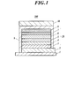
- FIG. 1 It is a schematic sectional drawing which shows an example of a structure of an organic electroluminescent element. It is drawing which shows roughly the Guinier plot of Example sample 1,6,7 and the comparative example sample 9.
- FIG. 1 It is a schematic sectional drawing which shows an example of a structure of an organic electroluminescent element. It is drawing which shows roughly the Guinier plot of Example sample 1,6,7 and the comparative example sample 9.
- an organic electroluminescence element 100 (hereinafter also referred to as an organic EL element) according to a preferred embodiment of the present invention has a flexible support substrate 1.
- An anode 2 is formed on the flexible support substrate 1
- an organic functional layer 20 is formed on the anode 2
- a cathode 8 is formed on the organic functional layer 20.
- the organic functional layer 20 refers to each layer constituting the organic electroluminescence element 100 provided between the anode 2 and the cathode 8.
- the organic functional layer 20 includes, for example, a hole injection layer 3, a hole transport layer 4, a light emitting layer 5, an electron transport layer 6, an electron injection layer 7, and in addition, a hole block layer, an electron block layer, and the like. May be included.
- the anode 2, the organic functional layer 20, and the cathode 8 on the flexible support substrate 1 are sealed with a flexible sealing member 10 through a sealing adhesive 9.
- these layer structures (refer FIG. 1) of the organic electroluminescent element 100 show only the preferable specific example, and this invention is not limited to these.
- the organic EL device 100 according to the present invention may have a layer structure of (i) to (viii).
- Organic functional layer 20 of organic EL element >> Subsequently, the detail of the organic functional layer which comprises the organic EL element of this invention is demonstrated.
- the injection layer can be provided as necessary.
- the injection layer includes an electron injection layer and a hole injection layer, and may be present between the anode and the light emitting layer or the hole transport layer and between the cathode and the light emitting layer or the electron transport layer as described above.
- the injection layer referred to in the present invention is a layer provided between the electrode and the organic functional layer in order to lower the driving voltage and improve the light emission luminance. “The organic EL element and its industrialization front line (November 30, 1998, NT.
- Injection materials include triazole derivatives, oxadiazole derivatives, imidazole derivatives, pyrazoline derivatives and pyrazolone derivatives, phenylenediamine derivatives, arylamine derivatives, amino-substituted chalcone derivatives, oxazole derivatives, styrylanthracene derivatives, fluorenone derivatives, hydrazone derivatives, stilbene derivatives.
- the details of the electron injection layer are described in, for example, JP-A-6-325871, JP-A-9-17574, and JP-A-10-74586, and specific examples thereof include strontium and aluminum.
- the buffer layer (injection layer) is desirably a very thin film, and potassium fluoride and sodium fluoride are preferable.
- the film thickness is about 0.1 nm to 5 ⁇ m, preferably 0.1 to 100 nm, more preferably 0.5 to 10 nm, and most preferably 0.5 to 4 nm.
- Hole transport layer 4 As the hole transport material constituting the hole transport layer, the same compounds as those applied in the hole injection layer can be used, and further, porphyrin compounds, aromatic tertiary amine compounds, and styryl. It is preferable to use an amine compound, particularly an aromatic tertiary amine compound.
- aromatic tertiary amine compounds and styrylamine compounds include N, N, N ′, N′-tetraphenyl-4,4′-diaminophenyl; N, N′-diphenyl-N, N′— Bis (3-methylphenyl)-[1,1′-biphenyl] -4,4′-diamine (TPD); 2,2-bis (4-di-p-tolylaminophenyl) propane; 1,1-bis (4-di-p-tolylaminophenyl) cyclohexane; N, N, N ′, N′-tetra-p-tolyl-4,4′-diaminobiphenyl; 1,1-bis (4-di-p-tolyl) Aminophenyl) -4-phenylcyclohexane; bis (4-dimethylamino-2-methylphenyl) phenylmethane; bis (4-di-p-tolylaminoph
- inorganic compounds such as p-type-Si and p-type-SiC can also be used as the hole injection material and the hole transport material.
- the hole transport layer is formed by thinning the hole transport material by a known method such as a vacuum deposition method, a spin coating method, a casting method, a printing method including an ink jet method, or an LB method. Can do.
- the thickness of the hole transport layer is not particularly limited, but is usually about 5 nm to 5 ⁇ m, preferably 5 to 200 nm.
- the hole transport layer may have a single layer structure composed of one or more of the above materials.
- n described in the above exemplary compounds represents the degree of polymerization and represents an integer having a weight average molecular weight in the range of 50,000 to 200,000. If the weight average molecular weight is less than this range, there is a concern of mixing with other layers during film formation due to the high solubility in the solvent. Even if a film can be formed, the light emission efficiency does not increase at a low molecular weight. When the weight average molecular weight is larger than this range, problems arise due to difficulty in synthesis and purification. Since the molecular weight distribution increases and the residual amount of impurities also increases, the light emission efficiency, voltage, and life of the organic EL element deteriorate. These polymer compounds are disclosed in Makromol. Chem. , Pages 193, 909 (1992) and the like.
- Electron transport layer 6 The electron transport layer is made of a material having a function of transporting electrons, and in a broad sense, an electron injection layer and a hole blocking layer are also included in the electron transport layer.
- the electron transport layer can be provided as a single layer or a plurality of layers. Conventionally, in the case of a single electron transport layer and a plurality of layers, an electron transport material (also serving as a hole blocking material) used for an electron transport layer adjacent to the cathode side with respect to the light emitting layer is injected from the cathode. As long as it has a function of transmitting electrons to the light-emitting layer, any material can be selected and used from among conventionally known compounds.
- fluorene derivatives for example, fluorene derivatives, carbazole derivatives, azacarbazole And metal complexes such as derivatives, oxadiazole derivatives, triazole derivatives, silole derivatives, pyridine derivatives, pyrimidine derivatives, 8-quinolinol derivatives, and the like.
- metal-free or metal phthalocyanine, or those having terminal ends substituted with an alkyl group or a sulfonic acid group can be preferably used as the electron transporting material.
- a carbazole derivative, an azacarbazole derivative, a pyridine derivative, and the like are preferable in the present invention, and an azacarbazole derivative is more preferable.
- the electron transport layer can be formed by thinning the electron transport material by a known method such as a spin coating method, a casting method, a printing method including an ink jet method, an LB method, and the like, preferably
- the electron transport material can be formed by a wet process using a coating solution containing a fluorinated alcohol solvent.
- the thickness of the electron transport layer is not particularly limited, but is usually about 5 nm to 5 ⁇ m, preferably 5 to 200 nm.
- the electron transport layer may have a single layer structure composed of one or more of the above materials.
- an electron transport layer having high n property doped with impurities as a guest material can be used.
- examples thereof include JP-A-4-297076, JP-A-10-270172, JP-A-2000-196140, 2001-102175, J.A. Appl. Phys. 95, 5773 (2004), and the like.
- the electron transport layer in the present invention preferably contains an organic alkali metal salt.
- organic substance but formate, acetate, propionic acid, butyrate, valerate, caproate, enanthate, caprylate, oxalate, malonate, succinate Benzoate, phthalate, isophthalate, terephthalate, salicylate, pyruvate, lactate, malate, adipate, mesylate, tosylate, benzenesulfonate ,
- the type of alkali metal of the alkali metal salt of the organic substance is not particularly limited, and examples thereof include Na, K, and Cs, preferably K, Cs, and more preferably Cs.
- Examples of the alkali metal salt of the organic substance include a combination of the organic substance and the alkali metal, preferably, formic acid Li, formic acid K, formic acid Na, formic acid Cs, acetic acid Li, acetic acid K, Na acetate, acetic acid Cs, propionic acid Li, Propionic acid Na, propionic acid K, propionic acid Cs, oxalic acid Li, oxalic acid Na, oxalic acid K, oxalic acid Cs, malonic acid Li, malonic acid Na, malonic acid K, malonic acid Cs, succinic acid Li, succinic acid Na, succinic acid K, succinic acid Cs, benzoic acid Li, benzoic acid Na, benzoic acid K, benzoic acid Li,
- the light emitting layer constituting the organic EL device of the present invention is a layer that emits light by recombination of electrons and holes injected from the electrode, the electron transport layer, or the hole transport layer, and the light emitting portion is the light emitting layer. It may be in the layer or the interface between the light emitting layer and the adjacent layer.
- the light emitting layer according to the present invention is not particularly limited in its configuration as long as the contained light emitting material satisfies the above requirements. Moreover, there may be a plurality of layers having the same emission spectrum and emission maximum wavelength. It is preferable to have a non-light emitting intermediate layer between each light emitting layer.
- the total thickness of the light emitting layers in the present invention is preferably in the range of 1 to 100 nm, and more preferably 50 nm or less because a lower driving voltage can be obtained.
- the sum total of the film thickness of the light emitting layer as used in this invention is a film thickness also including the said intermediate
- the film thickness of each light emitting layer is preferably adjusted in the range of 1 to 50 nm.
- each light emitting layer may emit light of each color of blue, green, and red, and there is no particular limitation on the relationship between the thickness of each light emitting layer.
- a plurality of light emitting materials may be mixed in each light emitting layer, and a phosphorescent light emitting material and a fluorescent light emitting material may be mixed and used in the same light emitting layer.
- the structure of the light-emitting layer preferably contains a host compound and a light-emitting material (also referred to as a light-emitting dopant compound) and emits light from the light-emitting material.
- (4.1) Host Compound As the host compound contained in the light emitting layer of the organic EL device of the present invention, a compound having a phosphorescence quantum yield of phosphorescence emission at room temperature (25 ° C.) of less than 0.1 is preferable. More preferably, the phosphorescence quantum yield is less than 0.01. Moreover, it is preferable that the volume ratio in the layer is 50% or more among the compounds contained in a light emitting layer.
- known host compounds may be used alone or in combination of two or more. By using a plurality of types of host compounds, it is possible to adjust the movement of charges, and the organic EL element can be made highly efficient. Moreover, it becomes possible to mix different light emission by using multiple types of luminescent material mentioned later, and can thereby obtain arbitrary luminescent colors.
- the light emitting host used in the present invention may be a conventionally known low molecular compound or a high molecular compound having a repeating unit, and a low molecular compound having a polymerizable group such as a vinyl group or an epoxy group (polymerizable light emission).
- a polymer material it is difficult to purify, and the phenomenon that the compound is difficult to escape such as swelling and gelation due to incorporation of the solvent is likely to occur. It is preferably not high, and specifically, a material having a molecular weight of 2,000 or less at the time of coating is preferably used, and a material having a molecular weight of 1,000 or less at the time of coating is more preferably used.
- the known host compound a compound having a hole transporting ability and an electron transporting ability, preventing an increase in the wavelength of light emission, and having a high Tg (glass transition temperature) is preferable.
- the glass transition point (Tg) is a value determined by a method based on JIS-K-7121 using DSC (Differential Scanning Colorimetry).
- Specific examples of known host compounds include compounds described in the following documents. For example, Japanese Patent Application Laid-Open Nos.
- the host compound used in the present invention is preferably a carbazole derivative.
- the host compound is preferably a compound represented by the general formula (1).
- X represents NR ′, O, S, CR′R ′′ or SiR′R ′′.
- R ′ and R ′′ each represent a hydrogen atom or a substituent.
- Ar represents an aromatic ring.
- N represents an integer of 0 to 8.
- examples of the substituent represented by R ′ and R ′′ include an alkyl group (for example, a methyl group, an ethyl group, a propyl group, an isopropyl group, a t-butyl group, a pentyl group, Hexyl group, octyl group, dodecyl group, tridecyl group, tetradecyl group, pentadecyl group, etc.), cycloalkyl group (for example, cyclopentyl group, cyclohexyl group, etc.), alkenyl group (for example, vinyl group, allyl group, etc.), alkynyl group ( For example, ethynyl group, propargyl group, etc.), aromatic hydrocarbon ring group (aromatic carbocyclic group, aryl group, etc.), for example, phenyl group, p-chlorophenyl group, mesity
- These substituents may be further substituted with the above substituents.
- a plurality of these substituents may be bonded to each other to form a ring.
- X is preferably NR ′ or O
- R ′ is an aromatic hydrocarbon group (also referred to as an aromatic carbocyclic group, an aryl group, etc., for example, a phenyl group, a p-chlorophenyl group, a mesityl group, A tolyl group, a xylyl group, a naphthyl group, an anthryl group, an azulenyl group, an acenaphthenyl group, a fluorenyl group, a phenanthryl group, an indenyl group, a pyrenyl group, a biphenylyl group), or an aromatic heterocyclic group (for example, a furyl group, a thienyl group, a pyridyl group) Group, pyridazinyl group, pyrimidinyl group, pyrazinyl group, triazinyl group, imidazolyl group,
- aromatic hydrocarbon group and aromatic heterocyclic group each may have a substituent represented by R ′ or R ′′ in X of the general formula (1).
- examples of the aromatic ring represented by Ar include an aromatic hydrocarbon ring and an aromatic heterocyclic ring.
- the aromatic ring may be a single ring or a condensed ring, and may be unsubstituted or may have a substituent represented by R ′ or R ′′ in X of the general formula (1).
- examples of the aromatic hydrocarbon ring represented by Ar include a benzene ring, biphenyl ring, naphthalene ring, azulene ring, anthracene ring, phenanthrene ring, pyrene ring, chrysene ring, naphthacene ring, triphenylene ring, o-terphenyl ring, m-terphenyl ring, p-terphenyl ring, acenaphthene ring, coronene ring, fluorene ring, fluoranthrene ring, naphthacene ring, pentacene ring, perylene ring, pentaphen ring, picene ring, pyrene ring, Examples include a pyranthrene ring and anthraanthrene ring. These rings may further have substituents represented by R ′ and R ′′ in X of the partial structure represented by the general
- examples of the aromatic heterocycle represented by Ar include a furan ring, a dibenzofuran ring, a thiophene ring, an oxazole ring, a pyrrole ring, a pyridine ring, a pyridazine ring, and a pyrimidine ring.
- These rings may further have substituents represented by R ′ and R ′′ in the general formula (1).
- the aromatic ring represented by Ar is preferably a carbazole ring, a carboline ring, a dibenzofuran ring, or a benzene ring, and more preferably a carbazole ring, A carboline ring and a benzene ring, more preferably a benzene ring having a substituent, and particularly preferably a benzene ring having a carbazolyl group.
- the aromatic ring represented by Ar is preferably a condensed ring of three or more rings, and the aromatic hydrocarbon condensed ring condensed with three or more rings is specifically exemplified.
- aromatic heterocycle condensed with three or more rings include an acridine ring, a benzoquinoline ring, a carbazole ring, a carboline ring, a phenazine ring, a phenanthridine ring, a phenanthroline ring, a carboline ring, a cyclazine ring, Quindrine ring, tepenidine ring, quinindrin ring, triphenodithiazine ring, triphenodioxazine ring, phenanthrazine ring, anthrazine ring, perimidine ring, diazacarbazole ring (any one of the carbon atoms constituting the carboline ring is a nitrogen atom) Phenanthroline ring, dibenzofuran ring, dibenzothiophene ring, naphthofuran ring, naphthothiophene ring, benzodifuran ring, benzodif
- n represents an integer of 0 to 8, preferably 0 to 2, particularly preferably 1 to 2 when X is O or S.
- a host compound having both a dibenzofuran ring and a carbazole ring is particularly preferable.
- Luminescent material (luminescent dopant)
- a fluorescent compound or a phosphorescent light-emitting material also referred to as a phosphorescent compound or a phosphorescent compound
- the phosphorescent material is a compound in which light emission from an excited triplet is observed. Specifically, it is a compound that emits phosphorescence at room temperature (25 ° C.) and has a phosphorescence quantum yield of 25 ° C.
- the phosphorescence quantum yield is preferably 0.1 or more.
- the phosphorescence quantum yield can be measured by the method described in Spectra II, page 398 (1992 edition, Maruzen) of Experimental Chemistry Course 4 of the 4th edition.
- the phosphorescence quantum yield in a solution can be measured using various solvents, but when using a phosphorescent material in the present invention, the above phosphorescence quantum yield (0.01 or more) is achieved in any solvent. It only has to be done.
- the energy transfer type that obtains light emission from the phosphorescent light emitting material by moving it, and the other is that the phosphorescent light emitting material becomes a carrier trap, and carrier recombination occurs on the phosphorescent light emitting material, and light emission from the phosphorescent light emitting material
- the excited state energy of the phosphorescent material is lower than the excited state energy of the host compound.
- the phosphorescent light-emitting material can be appropriately selected from known materials used for the light-emitting layer of the organic EL element, but is preferably a complex compound containing a group 8-10 metal in the periodic table of elements.
- the phosphorescent material according to the present embodiment includes at least one blue phosphorescent material, preferably at least one blue phosphorescent material and at least one bandgap energy lower than the blue phosphorescent material. And a phosphorescent material.
- R 1 represents a substituent.
- Z represents a nonmetallic atom group necessary to form a 5- to 7-membered ring.
- N1 represents an integer of 0 to 5.
- B 1 to B 5 represents a carbon atom, a nitrogen atom, an oxygen atom, or a sulfur atom, and at least one represents a nitrogen atom.
- M 1 represents a group 8 to group 10 metal in the periodic table.
- X 1 ” and “X 2 ” represent a carbon atom, a nitrogen atom, or an oxygen atom
- L 1 represents an atomic group that forms a bidentate ligand together with X 1 and X 2 .
- M1 represents an integer of 1, 2, or 3
- m2 represents an integer of 0, 1, or 2, but “m1 + m2” is 2 or 3.
- the phosphorescent compound represented by the general formula (2) according to the present invention has a HOMO of ⁇ 5.15 to ⁇ 3.50 eV, a LUMO of ⁇ 1.25 to +1.00 eV, and preferably a HOMO of ⁇ 4. .80 to -3.50 eV, and LUMO is -0.80 to +1.00 eV.
- examples of the substituent represented by R 1 include an alkyl group (eg, methyl group, ethyl group, propyl group, isopropyl group, tert-butyl group, Pentyl group, hexyl group, octyl group, dodecyl group, tridecyl group, tetradecyl group, pentadecyl group etc.), cycloalkyl group (eg cyclopentyl group, cyclohexyl group etc.), alkenyl group (eg vinyl group, allyl group etc.), Alkynyl group (for example, ethynyl group, propargyl group, etc.), aromatic hydrocarbon ring group (also called aromatic carbocyclic group, aryl group, etc.), for example, phenyl group, p-chlorophenyl group, mesityl group, tolyl group, xylyl
- alkyl group eg, methyl group
- Z represents a nonmetallic atom group necessary for forming a 5- to 7-membered ring.
- the 5- to 7-membered ring formed by Z include a benzene ring, naphthalene ring, pyridine ring, pyrimidine ring, pyrrole ring, thiophene ring, pyrazole ring, imidazole ring, oxazole ring and thiazole ring. Of these, a benzene ring is preferred.
- B 1 to B 5 represent a carbon atom, a nitrogen atom, an oxygen atom or a sulfur atom, and at least one represents a nitrogen atom.
- the aromatic nitrogen-containing heterocycle formed by these five atoms is preferably a monocycle. Examples include pyrrole ring, pyrazole ring, imidazole ring, triazole ring, tetrazole ring, oxazole ring, isoxazole ring, thiazole ring, isothiazole ring, oxadiazole ring, and thiadiazole ring.
- a pyrazole ring and an imidazole ring are preferable, and an imidazole ring in which B2 and B5 are nitrogen atoms is particularly preferable.
- These rings may be further substituted with the above substituents.
- Preferred as the substituent are an alkyl group and an aryl group, and more preferably an aryl group.
- L 1 represents an atomic group that forms a bidentate ligand together with X 1 and X 2 .
- Specific examples of the bidentate ligand represented by X 1 -L 1 -X 2 include, for example, substituted or unsubstituted phenylpyridine, phenylpyrazole, phenylimidazole, phenyltriazole, phenyltetrazole, pyrazabol, picolinic acid And acetylacetone. These groups may be further substituted with the above substituents.
- n1 represents an integer of 1, 2 or 3
- m2 represents an integer of 0, 1 or 2
- m1 + m2 is 2 or 3.
- the case where m2 is 0 is preferable.
- the metal represented by M 1 a transition metal element belonging to Group 8 to 10 of the periodic table (also simply referred to as a transition metal) is used, among which iridium and platinum are preferable, and iridium is more preferable.
- each layer of organic functional layer it is sufficient that at least one light emitting layer as a constituent layer is formed by a coating method, and the method for forming the other layers is not particularly limited to the coating method, and is necessary. In accordance with the above, it is also possible to form a film using an evaporation method or the like.
- a coating method (also referred to as a coating film forming method) is used as a method for forming a light emitting layer.
- a method for forming the light emitting layer there are a spin coat method, a cast method, an ink jet method, a spray method, a printing method, a slot type coater method and the like.
- the light emitting layer is preferably formed by a coating method such as a spin coating method, an ink jet method, a spray method, a printing method, or a slot coater method.
- the slot coater method is preferably used.
- the coating solution is dried.
- spin drying hot air drying, far-infrared drying, vacuum drying, reduced pressure drying, or the like can be applied.
- the “coating film-forming method” as used herein means a process from application of a coating solution to completion of drying of the coating solution.
- the present inventors prepared low molecular organic thin films formed so as to have the same film thickness by various coating film forming methods, and suppressed the size and content of contained microcrystals in the low molecular organic thin films.
- the coating solution for the light emitting layer is preferably composed of two or more mixed solvents.
- the film is preferably formed in a coating environment of 35 ° C. or higher, and preferably formed at 40 ° C. or higher. In the coating film forming method, in order to generate a supercooled state depending on the case, cooling may be performed after coating and drying.
- drying step after coating film formation spin drying, hot air drying, far infrared drying, vacuum drying, reduced pressure drying, or the like can be applied.
- These drying conditions are as follows.
- the coating solution for the light emitting layer is applied, the coating solution is dried, and the drying time is 5% of the final thickness after drying, the drying time is 3 Preferably, it is within 2 seconds, and more preferably within 2 seconds.
- the film becomes thinner as the thin film is formed and the drying proceeds. It becomes a thin film having a final film thickness after drying.
- the “film thickness that is 5% more than the final film thickness after drying” means, for example, that when a thin film having a final film thickness after drying of 50 nm is prepared, the film thickness is 52.5 nm. It corresponds to.
- a spectroscopic ellipsometer for example, UVISEL manufactured by Joban Yvon
- UVISEL manufactured by Joban Yvon
- the inventors of the present invention have found that the molecular weight of the host (host compound) in the formation of the light emitting layer is particularly low in the slope of the Guinier plot of the scattered light due to the low molecular weight organic substance in the X-ray small angle scattering measurement of the light emitting layer after coating film formation. That is, it is possible to form a thin film in which a material such as a vapor deposition film with little aggregation and voids is dispersed, and is preferable in relation to the characteristics (power efficiency and light emission lifetime) of the obtained organic EL element. I found that there is a relationship.
- the molecular weight of the low molecular weight organic substance, particularly the host, in the light emitting layer is preferably in the range of 400 to 2000, more preferably in the range of 400 to 800.
- “Molecular weight” as used herein is obtained using a conventionally known mass spectrum. For polymers (for example, those having a molecular weight of 10,000 or more), a conventionally known GPC (gel permeation chromatography) is used. Measured.
- the thin film sample was irradiated with 1 mm.
- a HUBER multi-axis diffractometer is used, the X-ray incident angle ⁇ is fixed at 0.2 °, and the thin film sample is irradiated.
- the detector uses a scintillation counter to measure scattered radiation from 2 to 43 °. went.
- the Guinier plot was used for the analysis of the obtained X-ray small angle scattering data.
- X-rays When X-rays are incident on a substance, a part is scattered by an electron cloud of each atom constituting the X-ray. From a small scattering angle range (2 to 8 ° in the present invention), information on a spatial level of several nanometers to several hundred nanometers can be obtained, and structural evaluation using this is X-ray small angle scattering.
- the scattering vector q is generally used instead of the scattering angle ⁇ . q is given by the following formula (i).
- the organic film is generally formed by a vapor deposition film from the viewpoint of uniform dispersion of molecules in the film and suppression of impurities.
- film formation by vapor deposition is time consuming and costly, it is a film with a low cost application method, and how close to the vapor deposition film or dispersibility higher than the vapor deposition film can be obtained, high power efficiency and long life It becomes an important factor.
- the inventors of the present invention have found that the slope of the Guinier plot obtained from the X-ray small angle scattering is 1 when the slope of the Guinier plot obtained from the X-ray small angle scattering of the light emitting layer formed by vapor deposition is 1.
- the slope of the Guinier plot obtained from X-ray small angle scattering of the layer is 1.75 times or less, it is possible to produce an organic electroluminescence device having high power efficiency and a long lifetime.
- the magnification is more preferably 1.5 times or less, and most preferably 1.3 times or less.
- the slope of the Guinier plot obtained from these X-ray small angle scatterings is preferably ⁇ 700 or more and 0 or less, more preferably ⁇ 500 or more and 0 or less, and ⁇ 400 or more and 0 or less for high power efficiency and long life. Most preferable from the viewpoint of chemical conversion.
- an electrode material made of a metal, an alloy, an electrically conductive compound or a mixture thereof having a high work function (4 eV or more) is preferably used.
- electrode materials include metals such as Au, and conductive transparent materials such as CuI, indium tin oxide (ITO), SnO 2 , and ZnO.
- conductive transparent materials such as CuI, indium tin oxide (ITO), SnO 2 , and ZnO.
- an amorphous material such as IDIXO (In 2 O 3 —ZnO) capable of forming a transparent conductive film may be used.
- these electrode materials may be formed into a thin film by a method such as vapor deposition or sputtering, and a desired shape pattern may be formed by a photolithography method, or when pattern accuracy is not so high (about 100 ⁇ m or more)
- a pattern may be formed through a mask having a desired shape at the time of vapor deposition or sputtering of the electrode material.
- wet film-forming methods such as a printing system and a coating system, can also be used.
- the transmittance is greater than 10%, and the sheet resistance as the anode is preferably several hundred ⁇ / ⁇ or less.
- the film thickness depends on the material, it is usually in the range of 10 to 1000 nm, preferably in the range of 10 to 200 nm.
- Cathode 8 a material having a low work function (4 eV or less) metal (referred to as an electron injecting metal), an alloy, an electrically conductive compound, and a mixture thereof as an electrode material is used.
- electrode materials include sodium, sodium-potassium alloy, magnesium, lithium, magnesium / copper mixture, magnesium / silver mixture, magnesium / aluminum mixture, magnesium / indium mixture, aluminum / aluminum oxide (Al 2 O 3 ) Mixtures, indium, lithium / aluminum mixtures, rare earth metals and the like.
- a mixture of an electron injecting metal and a second metal which is a stable metal having a larger work function than this for example, a magnesium / silver mixture, Magnesium / aluminum mixtures, magnesium / indium mixtures, aluminum / aluminum oxide (Al 2 O 3 ) mixtures, lithium / aluminum mixtures, aluminum and the like are preferred.
- the cathode can be produced by forming a thin film of these electrode materials by a method such as vapor deposition or sputtering.
- the sheet resistance as the cathode is preferably several hundred ⁇ / ⁇ or less, and the film thickness is usually selected in the range of 10 nm to 5 ⁇ m, preferably 50 to 200 nm.
- the film thickness is usually selected in the range of 10 nm to 5 ⁇ m, preferably 50 to 200 nm.
- the light emission luminance is improved, which is convenient.
- a transparent or translucent cathode can be produced by forming the above metal on the cathode with a film thickness of 1 to 20 nm and then forming the conductive transparent material mentioned in the description of the anode thereon. By applying this, an organic EL element in which both the anode and the cathode are transmissive can be produced.
- the support substrate (hereinafter also referred to as a substrate, substrate, substrate, support, etc.) that can be used in the organic EL device of the present invention is not particularly limited in the type of glass, plastic, etc., and is transparent. May be opaque. When extracting light from the support substrate side, the support substrate is preferably transparent. Examples of the transparent support substrate preferably used include glass, quartz, and a transparent resin film. Since the effect of suppressing high-temperature storage stability and chromaticity variation appears greatly in a flexible substrate than a rigid substrate, a particularly preferable support substrate has flexibility that can give flexibility to an organic EL element. Resin film.
- polyesters such as polyethylene terephthalate (PET) and polyethylene naphthalate (PEN), polyethylene, polypropylene, cellophane, cellulose diacetate, cellulose triacetate, cellulose acetate butyrate, cellulose acetate propionate (CAP), Cellulose esters such as cellulose acetate phthalate (TAC) and cellulose nitrate or derivatives thereof, polyvinylidene chloride, polyvinyl alcohol, polyethylene vinyl alcohol, syndiotactic polystyrene, polycarbonate, norbornene resin, polymethylpentene, polyether ketone, polyimide , Polyethersulfone (PES), polyphenylene sulfide, polysulfones Cycloolefin resins such as polyetherimide, polyetherketoneimide, polyamide, fluororesin, nylon, polymethylmethacrylate, acrylic or polyarylate, Arton (trade name, manufactured by JSR) or Appel (
- an inorganic film, an organic film or a hybrid film of both may be formed on the surface of the resin film.
- the film is preferably a high-barrier film having a degree of 10 ⁇ 3 cm 3 / (m 2 ⁇ 24 h ⁇ atm) or less and a water vapor permeability of 10 ⁇ 3 g / (m 2 ⁇ 24 h) or less.
- the degree is 10 ⁇ 5 g / (m 2 ⁇ 24 h) or less.
- a material for forming the barrier film any material may be used as long as it has a function of suppressing entry of factors that cause deterioration of the organic EL element such as moisture and oxygen.
- silicon oxide, silicon dioxide, silicon nitride, or the like is used. Can do.
- the method for forming the barrier film is not particularly limited.
- a plasma CVD method, a laser CVD method, a thermal CVD method, a coating method, and the like can be used, but an atmospheric pressure plasma polymerization method as described in JP-A-2004-68143 is particularly preferable.
- the opaque support substrate examples include metal plates such as aluminum and stainless steel, films, opaque resin substrates, and ceramic substrates.
- the external extraction efficiency of light emission at room temperature is preferably 1% or more, more preferably 5% or more.
- the external extraction quantum efficiency (%) the number of photons emitted to the outside of the organic EL element / the number of electrons sent to the organic EL element ⁇ 100.
- Sealing (sealing adhesive 9, sealing member 10)
- a sealing means applicable to the organic EL element of the present invention for example, a method of adhering a sealing member, an electrode, and a support substrate with an adhesive can be mentioned.
- a sealing member it should just be arrange
- Examples of the glass plate include soda-lime glass, barium / strontium-containing glass, lead glass, aluminosilicate glass, borosilicate glass, barium borosilicate glass, and quartz.
- Examples of the polymer plate include polycarbonate, acrylic, polyethylene terephthalate, polyether sulfide, and polysulfone.
- Examples of the metal plate include those made of one or more metals or alloys selected from the group consisting of stainless steel, iron, copper, aluminum, magnesium, nickel, zinc, chromium, titanium, molybdenum, silicone, germanium, and tantalum.
- a polymer film and a metal film can be preferably used because the element can be thinned.
- the polymer film has an oxygen permeability measured by a method according to JIS K 7126-1987 of 1 ⁇ 10 ⁇ 3 cm 3 / (m 2 ⁇ 24 h ⁇ atm) or less, and conforms to JIS K 7129-1992.
- the water vapor permeability (25 ⁇ 0.5 ° C., relative humidity (90 ⁇ 2)% RH) measured by the above method is preferably 1 ⁇ 10 ⁇ 3 g / (m 2 ⁇ 24 h) or less.
- sandblasting, chemical etching, or the like is used for processing the sealing member into a concave shape.
- the adhesive include photocuring and thermosetting adhesives having reactive vinyl groups of acrylic acid oligomers and methacrylic acid oligomers, and moisture curing adhesives such as 2-cyanoacrylates. Can be mentioned. Moreover, heat
- coating of the adhesive agent to a sealing part may use commercially available dispenser, and may print like screen printing.
- the electrode and the organic functional layer are coated on the outside of the electrode facing the support substrate with the organic functional layer interposed therebetween, and an inorganic or organic layer is formed in contact with the support substrate to form a sealing film.
- the material for forming the film may be any material that has a function of suppressing intrusion of elements that cause deterioration of elements such as moisture and oxygen.
- silicon oxide, silicon dioxide, silicon nitride, or the like may be used. it can.
- vacuum deposition sputtering, reactive sputtering, molecular beam epitaxy, cluster ion beam method, ion plating method, plasma polymerization method, atmospheric pressure plasma
- a polymerization method a plasma CVD method, a laser CVD method, a thermal CVD method, a coating method, or the like can be used.
- an inert gas such as nitrogen or argon, an inert gas such as fluorinated hydrocarbon or silicon oil is used. It is preferable to inject a liquid. A vacuum is also possible.
- a hygroscopic compound can also be enclosed inside. Examples of the hygroscopic compound include metal oxides (for example, sodium oxide, potassium oxide, calcium oxide, barium oxide, magnesium oxide, aluminum oxide) and sulfates (for example, sodium sulfate, calcium sulfate, magnesium sulfate, cobalt sulfate).
- metal halides eg calcium chloride, magnesium chloride, cesium fluoride, tantalum fluoride, cerium bromide, magnesium bromide, barium iodide, magnesium iodide etc.
- perchloric acids eg perchloric acid Barium, magnesium perchlorate, and the like
- anhydrous salts are preferably used in sulfates, metal halides, and perchloric acids.
- Sealing includes casing type sealing (can sealing) and close contact type sealing (solid sealing), but solid sealing is preferable from the viewpoint of thinning. Moreover, when producing a flexible organic EL element, since sealing is also required for the sealing member, solid sealing is preferable.
- thermosetting adhesive such as an epoxy resin, an acrylic resin, or a silicone resin, more preferably moisture resistant.
- a thermosetting adhesive such as an epoxy resin, an acrylic resin, or a silicone resin, more preferably moisture resistant.
- It is an epoxy thermosetting adhesive resin that is excellent in water resistance and water resistance and has little shrinkage during curing.
- the water content of the sealing adhesive according to the present invention is preferably 300 ppm or less, more preferably 0.01 to 200 ppm, and most preferably 0.01 to 100 ppm.
- the moisture content referred to in the present invention may be measured by any method.
- a volumetric moisture meter Karl Fischer
- an infrared moisture meter a microwave transmission moisture meter
- a heat-dry weight method GC / MS , IR, DSC (differential scanning calorimeter), TDS (temperature programmed desorption analysis).
- a precision moisture meter AVM-3000 Omnitech
- moisture can be measured from a pressure increase caused by evaporation of moisture, and moisture content of a film or a solid film can be measured.
- the moisture content of the sealing adhesive can be adjusted by, for example, placing it in a nitrogen atmosphere with a dew point temperature of ⁇ 80 ° C. or lower and an oxygen concentration of 0.8 ppm, and changing the time.
- the sealing adhesive can be dried in a vacuum state of 100 Pa or less while changing the time.
- the sealing adhesive can be dried only with an adhesive, but can also be placed in advance on the sealing member and dried.
- the sealing member for example, a 50 ⁇ m thick PET (polyethylene terephthalate) laminated with an aluminum foil (30 ⁇ m thick) is used.
- a sealing adhesive is placed in advance, the resin substrate 1 and the sealing member 5 are aligned, and both are pressure-bonded ( 0.1-3 MPa) and a temperature of 80-180 ° C. for close contact / bonding (adhesion), and close sealing (solid sealing).
- Heating or pressure bonding time varies depending on the type, amount, and area of the adhesive, but temporary bonding is performed at a pressure of 0.1 to 3 MPa, and heat curing time is in the range of 5 seconds to 10 minutes at a temperature of 80 to 180 ° C. Just choose.
- the use of a heated crimping roll is preferred because it allows simultaneous crimping (temporary bonding) and heating, and eliminates internal voids at the same time.
- a coating method such as roll coating, spin coating, screen printing, or spray coating, or a printing method can be used depending on the material.
- solid sealing is a form in which there is no space between the sealing member and the organic EL element substrate and the resin is covered with a cured resin.
- the sealing member include metals such as stainless steel, aluminum, and magnesium alloys, polyethylene terephthalate, polycarbonate, polystyrene, nylon, plastics such as polyvinyl chloride, and composites thereof, glass, and the like.
- a laminate of gas barrier layers such as aluminum, aluminum oxide, silicon oxide, and silicon nitride can be used as in the case of a resin substrate.
- the gas barrier layer can be formed by sputtering, vapor deposition or the like on both surfaces or one surface of the sealing member before molding the sealing member, or may be formed on both surfaces or one surface of the sealing member after sealing by a similar method.
- the oxygen permeability is 1 ⁇ 10 ⁇ 3 ml / (m 2 ⁇ 24 h ⁇ atm) or less
- the water vapor permeability (25 ⁇ 0.5 ° C., relative humidity (90 ⁇ 2)% RH) is 1 ⁇ It is preferably 10 ⁇ 3 g / (m 2 ⁇ 24 h) or less.
- the sealing member may be a film laminated with a metal foil such as aluminum.
- a generally used laminating machine can be used.
- the adhesive polyurethane-based, polyester-based, epoxy-based, acrylic-based adhesives and the like can be used. You may use a hardening
- a hot melt lamination method, an extrusion lamination method and a coextrusion lamination method can also be used, but a dry lamination method is preferred.
- the metal foil is formed by sputtering or vapor deposition and is formed from a fluid electrode material such as a conductive paste, it may be created by a method of forming a metal foil on a polymer film as a base. Good.
- a protective film or a protective plate may be provided outside the sealing film on the side facing the support substrate with the organic functional layer interposed therebetween or on the outer side of the sealing film.
- the mechanical strength is not necessarily high, and thus it is preferable to provide such a protective film and a protective plate.
- the same glass plate, polymer plate / film, metal plate / film, and the like used for the sealing can be used.
- the polymer film is light and thin. Is preferably used.
- a light extraction member between the flexible support substrate and the anode, or at any location on the light emission side from the flexible support substrate.
- the light extraction member include a prism sheet, a lens sheet, and a diffusion sheet.
- a diffraction grating or a diffusion structure introduced into an interface or any medium that causes total reflection can be used.
- an organic electroluminescence element that emits light from a substrate
- a part of the light emitted from the light emitting layer causes total reflection at the interface between the substrate and air, causing a problem of loss of light.
- prismatic or lens-like processing is applied to the surface of the substrate, or prism sheets, lens sheets, and diffusion sheets are affixed to the surface of the substrate, thereby suppressing total reflection and light extraction efficiency.
- prismatic or lens-like processing is applied to the surface of the substrate, or prism sheets, lens sheets, and diffusion sheets are affixed to the surface of the substrate, thereby suppressing total reflection and light extraction efficiency.
- a method of introducing a diffraction grating or a method of introducing a diffusion structure in an interface or any medium that causes total reflection is known.
- Method for Manufacturing Organic EL Element 100 As an example of the method for producing an organic EL device of the present invention, a method for producing an organic EL device comprising an anode / hole injection layer / hole transport layer / light emitting layer / electron transport layer / electron injection layer / cathode will be described.
- a desired electrode material for example, a thin film made of an anode material is formed on a suitable substrate by a thin film forming method such as vapor deposition or sputtering so as to have a thickness of 1 ⁇ m or less, preferably 10 to 200 nm.
- An anode is produced.
- a hole injection layer, a hole transport layer, a light emitting layer, an electron transport layer, and an organic functional layer (organic compound thin film) of an electron injection layer, which are organic EL element materials, are formed thereon.
- the process of forming the organic functional layer mainly includes (I) a step of applying and laminating the coating liquid constituting the organic functional layer on the anode of the support substrate; (Ii) a step of drying the coating solution after coating and lamination; Consists of.
- the light emitting layer forming method (coating film forming method) is as described above.
- a vapor deposition method for example, spin coating method, casting method, die coating method, blade coating method, roll coating method, ink jet method, printing method, spray coating).
- Method, curtain coating method, LB method Liangmuir Brodgett method and the like can be used
- at least the light emitting layer of the present invention is preferably formed by a wet process.
- a wet process in the present invention because it is easy to obtain a homogeneous film and it is difficult to generate pinholes.
- Film formation by a coating method such as a die coating method, a blade coating method, a roll coating method, or an ink jet method is preferable.
- the liquid medium for dissolving or dispersing the organic EL material according to the present invention include ketones such as methyl ethyl ketone and cyclohexanone, fatty acid esters such as ethyl acetate, halogenated hydrocarbons such as dichlorobenzene, toluene, xylene, and mesitylene.
- Aromatic hydrocarbons such as cyclohexylbenzene, aliphatic hydrocarbons such as cyclohexane, decalin, and dodecane, and organic solvents such as dimethylformamide (DMF) and dimethylsulfoxide (DMSO) can be used.
- a dispersion method it can disperse
- the preparation step for dissolving or dispersing the organic EL material according to the present invention and the coating process until coating on the substrate are preferably performed under an inert gas atmosphere. Even if it is not performed, film formation can be performed without degrading the performance of the organic EL element, and thus it may not always be performed in an inert gas atmosphere. In this case, the manufacturing cost can be suppressed, which is more preferable.
- the coated and laminated organic functional layer is dried.
- drying refers to a reduction to 0.2% or less when the solvent content of the film immediately after coating is 100%.
- those generally used can be used, and examples thereof include reduced pressure or pressure drying, heat drying, air drying, IR drying, and electromagnetic wave drying.
- heat drying is preferable, the temperature is equal to or higher than the boiling point of the solvent having the lowest boiling point in the organic functional layer coating solvent, and the temperature is lower than (Tg + 20) ° C. of the material having the lowest Tg among the Tg of the organic functional layer material. Most preferably, it is held at In the present invention, more specifically, it is preferable to hold and dry at 80 ° C.
- the atmosphere at the time of drying the coating liquid after coating / lamination is preferably an atmosphere having a volume concentration of a gas other than the inert gas of 200 ppm or less. It may not be necessary to do this. In this case, the manufacturing cost can be suppressed, which is more preferable.
- the inert gas is preferably a rare gas such as nitrogen gas and argon gas, and most preferably nitrogen gas in terms of production cost.
- the coating / laminating and drying steps of these layers may be single wafer manufacturing or line manufacturing. Further, the drying process may be performed while being conveyed on the line, but from the viewpoint of productivity, it may be deposited or rolled in a non-contact manner in a roll form.
- a thin film made of a cathode material is formed thereon by a method such as vapor deposition or sputtering so as to have a film thickness of 1 ⁇ m or less, preferably in the range of 50 nm to 200 nm.
- a desired organic EL element can be obtained.
- the organic EL element can be produced by adhering the close-sealing or sealing member to the electrode and the support substrate with an adhesive.
- the organic EL element of the present invention can be used as a display device, a display, and various light emission sources.
- light sources include home lighting, interior lighting, clock and liquid crystal backlights, billboard advertisements, traffic lights, light sources for optical storage media, light sources for electrophotographic copying machines, light sources for optical communication processors, and light sources for optical sensors.
- it can be used in a wide range of applications such as general household appliances that require a display device, but it can be used effectively as a backlight for a liquid crystal display device combined with a color filter, and as a light source for illumination. it can.
- patterning may be performed by a metal mask, an ink jet printing method, or the like as needed during film formation. In the case of patterning, only the electrode may be patterned, the electrode and the light emitting layer may be patterned, or the entire layer of the element may be patterned. In the fabrication of the element, a conventionally known method is used. Can do.
- Example Sample 1 Production of Gas Barrier Flexible Film First of polyethylene naphthalate film (Teijin DuPont film, hereinafter abbreviated as PEN) as the flexible film.
- An inorganic gas barrier film made of SiOx is continuously formed on the flexible film by using an atmospheric pressure plasma discharge treatment apparatus having a structure described in JP-A-2004-68143 on the entire surface on the electrode forming side.
- first electrode layer 120 nm thick ITO (Indium Tin Oxide) film is formed on the prepared gas barrier flexible film by sputtering and patterned by photolithography. An electrode layer (anode) was formed. The pattern was such that the light emission area was 50 mm square.
- ITO Indium Tin Oxide
- each light-emitting layer composition having the following composition was formed by spin coating at 1500 rpm for 30 seconds, and then held at 120 ° C. for 30 minutes to form a light-emitting layer having a thickness of 40 nm. did.
- ⁇ Light emitting layer composition> Host material ...
- Exemplary compound D-80 0.025 Part by mass Solvent type: Toluene: Isopropyl acetate 1: 1 2,000 parts by mass
- the drying liquid was applied to the coating solution while maintaining the environmental temperature at 40 ° C. during the coating.
- Example Sample 1 (organic EL element).
- a sealing member a flexible aluminum foil (manufactured by Toyo Aluminum Co., Ltd.) having a thickness of 30 ⁇ m and a polyethylene terephthalate (PET) film (12 ⁇ m thickness) as an adhesive for dry lamination (two-component reactive urethane) (Adhesive layer thickness 1.5 ⁇ m) was used.
- PET polyethylene terephthalate
- Adhesive layer thickness 1.5 ⁇ m As a sealing adhesive, a thermosetting adhesive was uniformly applied to the aluminum surface with a thickness of 20 ⁇ m along the adhesive surface (shiny surface) of the aluminum foil using a dispenser.
- thermosetting adhesive an epoxy adhesive mixed with the following (A) to (C) was used.
- DGEBA Bisphenol A diglycidyl ether
- DIY Dicyandiamide
- C Epoxy adduct curing accelerator
- Example sample 1 (organic EL element) was manufactured by closely sealing at a temperature of 120 ° C., a pressure of 0.5 MPa, and an apparatus speed of 0.3 m / min.
- Example Sample 2 Preparation of Example Samples 2 to 5 In Example Samples 2 to 5, D-1 and D-2 were reduced from the dopant material, and the coating and drying environment (solvent type, coating temperature, drying Presence or absence, drying time, etc.). Other than that was the same as Example Sample 1.
- Example Sample 6 In Example Sample 6, a-20, a-27, and a-38 were reduced from the host material. Other than that was the same as Example Sample 2.
- Example Sample 7 In Example Sample 7, a-7 was reduced from the host material.
- Example Sample 6 (5) Production of Example Sample 8 In Example Sample 8, a-2 was reduced from the host material.
- Example Sample 9 (Coating) The light emitting layer composition was changed to the following composition. Other than that was the same as Example Sample 1.
- Comparative Example Sample 10 (Vapor Deposition)
- the light emitting layer having the same configuration as that of Comparative Example Sample 9 with the solvent removed is used as the vapor deposition source, and only the light emitting layer is formed on the silicon wafer by vapor deposition. Filmed.
- Table 1 shows the compositions, coating and drying environments (conditions), etc. of Example Samples 1 to 8 and Comparative Samples 9 to 10 described above.
- Yield rate calculation 10 samples were prepared for each sample, and all samples were lit at room temperature (about 23 to 25 ° C.) under a constant luminance condition of 1,000 cd / m 2 to emit no light ( The presence or absence of dark spots) was examined. The inside of the light emitting element of each sample was divided into 5 ⁇ 5 square areas, the areas where dark spots were seen were treated as defective areas, and the ratio of defective areas to all 250 areas (yield rate (%)) was obtained. The evaluation results are shown in Table 2.
- Example Samples 1 to 8 have good results in each evaluation. there were. From the above, in order to at least improve the luminous efficiency, reduce the driving voltage, and improve the luminous lifetime, the slope of the Guinier plot of the light emitting layer is 1.75 times or less than that of the light emitting layer formed by vapor deposition. It turns out that is useful.
- the present invention can be particularly suitably used to realize high luminous efficiency, low driving voltage, and long life as the characteristics of the organic EL element.
Landscapes
- Chemical & Material Sciences (AREA)
- Organic Chemistry (AREA)
- Engineering & Computer Science (AREA)
- Materials Engineering (AREA)
- Manufacturing & Machinery (AREA)
- Physics & Mathematics (AREA)
- Optics & Photonics (AREA)
- Electroluminescent Light Sources (AREA)
- Nitrogen And Oxygen Or Sulfur-Condensed Heterocyclic Ring Systems (AREA)
Abstract
L'invention concerne un élément électroluminescent organique (100) qui comprend, sur un substrat (1), une paire d'électrodes (2, 8) et au moins une couche d'émission de lumière (5). La couche d'émission de lumière (5) contient au moins un type de dopant et au moins un type d'hôte. La couche d'émission de lumière (100) est formée par un procédé de revêtement utilisant une solution de revêtement dispersée dans au moins un type de solvant, et la pente d'une représentation de Guinier obtenue à partir d'une dispersion de rayons X à angle faible est de 1,75 fois au moins la pente d'une représentation de Guinier obtenue par une dispersion de rayons X à angle faible d'une couche d'émission de lumière comparative formée par dépôt en phase vapeur.
Priority Applications (1)
| Application Number | Priority Date | Filing Date | Title |
|---|---|---|---|
| JP2013516235A JP5862663B2 (ja) | 2011-05-24 | 2012-03-12 | 有機エレクトロルミネッセンス素子の製造方法 |
Applications Claiming Priority (2)
| Application Number | Priority Date | Filing Date | Title |
|---|---|---|---|
| JP2011-115615 | 2011-05-24 | ||
| JP2011115615 | 2011-05-24 |
Publications (1)
| Publication Number | Publication Date |
|---|---|
| WO2012160859A1 true WO2012160859A1 (fr) | 2012-11-29 |
Family
ID=47216948
Family Applications (1)
| Application Number | Title | Priority Date | Filing Date |
|---|---|---|---|
| PCT/JP2012/056229 Ceased WO2012160859A1 (fr) | 2011-05-24 | 2012-03-12 | Elément électroluminescent organique, dispositif d'affichage et dispositif d'éclairage |
Country Status (2)
| Country | Link |
|---|---|
| JP (1) | JP5862663B2 (fr) |
| WO (1) | WO2012160859A1 (fr) |
Cited By (3)
| Publication number | Priority date | Publication date | Assignee | Title |
|---|---|---|---|---|
| WO2014013721A1 (fr) * | 2012-07-20 | 2014-01-23 | 出光興産株式会社 | Composé cyclique hétéro-aromatique d'azote, et élément électroluminescent organique mettant en œuvre celui-ci |
| WO2014088300A1 (fr) * | 2012-12-04 | 2014-06-12 | Rohm And Haas Electronic Materials Korea Ltd. | Composés à électroluminescence organique et dispositif à électroluminescence organique les comprenant |
| US12501828B2 (en) | 2018-12-28 | 2025-12-16 | Samsung Electronics Co., Ltd. | Organic light-emitting device and apparatus including the same |
Citations (5)
| Publication number | Priority date | Publication date | Assignee | Title |
|---|---|---|---|---|
| JP2004231784A (ja) * | 2003-01-30 | 2004-08-19 | Konica Minolta Holdings Inc | 有機−無機ポリマーハイブリッドフィルム、その製造方法、該フィルムを用いたディスプレイ及びタッチパネル |
| JP2006066294A (ja) * | 2004-08-27 | 2006-03-09 | Hitachi Displays Ltd | 電子装置の製造方法およびこの製造に用いる非晶質薄膜形成用インク組成物 |
| JP2006148045A (ja) * | 2004-11-17 | 2006-06-08 | Samsung Sdi Co Ltd | 低分子有機電界発光素子及びその製造方法 |
| JP2010278287A (ja) * | 2009-05-29 | 2010-12-09 | Konica Minolta Holdings Inc | 有機エレクトロルミネッセンス素子、該素子を用いた表示装置、照明装置及び有機エレクトロルミネッセンス素子の製造方法 |
| WO2011024922A1 (fr) * | 2009-08-27 | 2011-03-03 | 三菱化学株式会社 | Composé monoamine, matière de transport de charge, composition pour un film de transport de charge, élément électroluminescent organique, dispositif d'affichage électroluminescent organique et dispositif d'éclairage électroluminescent organique |
-
2012
- 2012-03-12 WO PCT/JP2012/056229 patent/WO2012160859A1/fr not_active Ceased
- 2012-03-12 JP JP2013516235A patent/JP5862663B2/ja not_active Expired - Fee Related
Patent Citations (5)
| Publication number | Priority date | Publication date | Assignee | Title |
|---|---|---|---|---|
| JP2004231784A (ja) * | 2003-01-30 | 2004-08-19 | Konica Minolta Holdings Inc | 有機−無機ポリマーハイブリッドフィルム、その製造方法、該フィルムを用いたディスプレイ及びタッチパネル |
| JP2006066294A (ja) * | 2004-08-27 | 2006-03-09 | Hitachi Displays Ltd | 電子装置の製造方法およびこの製造に用いる非晶質薄膜形成用インク組成物 |
| JP2006148045A (ja) * | 2004-11-17 | 2006-06-08 | Samsung Sdi Co Ltd | 低分子有機電界発光素子及びその製造方法 |
| JP2010278287A (ja) * | 2009-05-29 | 2010-12-09 | Konica Minolta Holdings Inc | 有機エレクトロルミネッセンス素子、該素子を用いた表示装置、照明装置及び有機エレクトロルミネッセンス素子の製造方法 |
| WO2011024922A1 (fr) * | 2009-08-27 | 2011-03-03 | 三菱化学株式会社 | Composé monoamine, matière de transport de charge, composition pour un film de transport de charge, élément électroluminescent organique, dispositif d'affichage électroluminescent organique et dispositif d'éclairage électroluminescent organique |
Cited By (3)
| Publication number | Priority date | Publication date | Assignee | Title |
|---|---|---|---|---|
| WO2014013721A1 (fr) * | 2012-07-20 | 2014-01-23 | 出光興産株式会社 | Composé cyclique hétéro-aromatique d'azote, et élément électroluminescent organique mettant en œuvre celui-ci |
| WO2014088300A1 (fr) * | 2012-12-04 | 2014-06-12 | Rohm And Haas Electronic Materials Korea Ltd. | Composés à électroluminescence organique et dispositif à électroluminescence organique les comprenant |
| US12501828B2 (en) | 2018-12-28 | 2025-12-16 | Samsung Electronics Co., Ltd. | Organic light-emitting device and apparatus including the same |
Also Published As
| Publication number | Publication date |
|---|---|
| JP5862663B2 (ja) | 2016-02-16 |
| JPWO2012160859A1 (ja) | 2014-07-31 |
Similar Documents
| Publication | Publication Date | Title |
|---|---|---|
| JP6052324B2 (ja) | 有機エレクトロルミネッセンス素子 | |
| JP6128119B2 (ja) | 有機エレクトロルミネッセンス素子、有機エレクトロルミネッセンス素子の製造方法、表示装置および照明装置 | |
| JP5664311B2 (ja) | 有機エレクトロルミネッセンス素子 | |
| JPWO2012121101A1 (ja) | 有機エレクトロルミネッセンス素子 | |
| JP5561272B2 (ja) | 有機エレクトロルミネッセンス素子 | |
| JP2013200941A (ja) | 有機エレクトロルミネッセンス素子の製造方法 | |
| JP5765271B2 (ja) | 有機エレクトロルミネッセンス素子、表示装置および照明装置 | |
| JP5817490B2 (ja) | 有機エレクトロルミネッセンス素子、表示装置及び照明装置 | |
| JP5790536B2 (ja) | 有機エレクトロルミネッセンス素子及びその製造方法 | |
| WO2012077431A1 (fr) | Procédé de fabrication d'élément électroluminescent organique | |
| JP5862663B2 (ja) | 有機エレクトロルミネッセンス素子の製造方法 | |
| JP5958464B2 (ja) | 有機エレクトロルミネッセンス素子およびその製造方法 | |
| WO2013141190A1 (fr) | Élément d'étanchéité pour élément à électroluminescence organique et procédé pour fabriquer l'élément à électroluminescence organique | |
| WO2013080696A1 (fr) | Elément électroluminescente (el) organique | |
| JP5983618B2 (ja) | 有機エレクトロルミネッセンス素子の製造方法 | |
| JP6052326B2 (ja) | 有機エレクトロルミネッセンス素子、表示装置及び照明装置 | |
| JP2013074085A (ja) | 有機エレクトロルミネッセンス素子 | |
| JP5867189B2 (ja) | 有機エレクトロルミネッセンス素子、表示装置及び照明装置 | |
| JP5655616B2 (ja) | 有機エレクトロルミネッセンス素子及び有機エレクトロルミネッセンス素子の製造方法 | |
| JP2014103290A (ja) | 有機エレクトロルミネッセンス素子、有機エレクトロルミネッセンス素子の製造方法及び金属酸化物粒子含有組成物 | |
| JPWO2011114870A1 (ja) | 有機エレクトロルミネッセンス素子の製造方法 | |
| JPWO2013031346A1 (ja) | 有機エレクトロルミネッセンス素子ならびに表示装置および照明装置 |
Legal Events
| Date | Code | Title | Description |
|---|---|---|---|
| 121 | Ep: the epo has been informed by wipo that ep was designated in this application |
Ref document number: 12790165 Country of ref document: EP Kind code of ref document: A1 |
|
| ENP | Entry into the national phase |
Ref document number: 2013516235 Country of ref document: JP Kind code of ref document: A |
|
| NENP | Non-entry into the national phase |
Ref country code: DE |
|
| 122 | Ep: pct application non-entry in european phase |
Ref document number: 12790165 Country of ref document: EP Kind code of ref document: A1 |