WO2012164882A1 - Substrat pour dispositif d'affichage et dispositif d'affichage le comprenant - Google Patents
Substrat pour dispositif d'affichage et dispositif d'affichage le comprenant Download PDFInfo
- Publication number
- WO2012164882A1 WO2012164882A1 PCT/JP2012/003399 JP2012003399W WO2012164882A1 WO 2012164882 A1 WO2012164882 A1 WO 2012164882A1 JP 2012003399 W JP2012003399 W JP 2012003399W WO 2012164882 A1 WO2012164882 A1 WO 2012164882A1
- Authority
- WO
- WIPO (PCT)
- Prior art keywords
- substrate
- display device
- wiring
- insulating film
- tft
- Prior art date
- Legal status (The legal status is an assumption and is not a legal conclusion. Google has not performed a legal analysis and makes no representation as to the accuracy of the status listed.)
- Ceased
Links
Images







Classifications
-
- H—ELECTRICITY
- H10—SEMICONDUCTOR DEVICES; ELECTRIC SOLID-STATE DEVICES NOT OTHERWISE PROVIDED FOR
- H10D—INORGANIC ELECTRIC SEMICONDUCTOR DEVICES
- H10D86/00—Integrated devices formed in or on insulating or conducting substrates, e.g. formed in silicon-on-insulator [SOI] substrates or on stainless steel or glass substrates
- H10D86/40—Integrated devices formed in or on insulating or conducting substrates, e.g. formed in silicon-on-insulator [SOI] substrates or on stainless steel or glass substrates characterised by multiple TFTs
- H10D86/411—Integrated devices formed in or on insulating or conducting substrates, e.g. formed in silicon-on-insulator [SOI] substrates or on stainless steel or glass substrates characterised by multiple TFTs characterised by materials, geometry or structure of the substrates
-
- H—ELECTRICITY
- H10—SEMICONDUCTOR DEVICES; ELECTRIC SOLID-STATE DEVICES NOT OTHERWISE PROVIDED FOR
- H10D—INORGANIC ELECTRIC SEMICONDUCTOR DEVICES
- H10D30/00—Field-effect transistors [FET]
- H10D30/60—Insulated-gate field-effect transistors [IGFET]
- H10D30/67—Thin-film transistors [TFT]
- H10D30/6758—Thin-film transistors [TFT] characterised by the insulating substrates
-
- H—ELECTRICITY
- H10—SEMICONDUCTOR DEVICES; ELECTRIC SOLID-STATE DEVICES NOT OTHERWISE PROVIDED FOR
- H10D—INORGANIC ELECTRIC SEMICONDUCTOR DEVICES
- H10D86/00—Integrated devices formed in or on insulating or conducting substrates, e.g. formed in silicon-on-insulator [SOI] substrates or on stainless steel or glass substrates
- H10D86/40—Integrated devices formed in or on insulating or conducting substrates, e.g. formed in silicon-on-insulator [SOI] substrates or on stainless steel or glass substrates characterised by multiple TFTs
- H10D86/451—Integrated devices formed in or on insulating or conducting substrates, e.g. formed in silicon-on-insulator [SOI] substrates or on stainless steel or glass substrates characterised by multiple TFTs characterised by the compositions or shapes of the interlayer dielectrics
-
- H—ELECTRICITY
- H10—SEMICONDUCTOR DEVICES; ELECTRIC SOLID-STATE DEVICES NOT OTHERWISE PROVIDED FOR
- H10D—INORGANIC ELECTRIC SEMICONDUCTOR DEVICES
- H10D86/00—Integrated devices formed in or on insulating or conducting substrates, e.g. formed in silicon-on-insulator [SOI] substrates or on stainless steel or glass substrates
- H10D86/40—Integrated devices formed in or on insulating or conducting substrates, e.g. formed in silicon-on-insulator [SOI] substrates or on stainless steel or glass substrates characterised by multiple TFTs
- H10D86/60—Integrated devices formed in or on insulating or conducting substrates, e.g. formed in silicon-on-insulator [SOI] substrates or on stainless steel or glass substrates characterised by multiple TFTs wherein the TFTs are in active matrices
-
- G—PHYSICS
- G02—OPTICS
- G02F—OPTICAL DEVICES OR ARRANGEMENTS FOR THE CONTROL OF LIGHT BY MODIFICATION OF THE OPTICAL PROPERTIES OF THE MEDIA OF THE ELEMENTS INVOLVED THEREIN; NON-LINEAR OPTICS; FREQUENCY-CHANGING OF LIGHT; OPTICAL LOGIC ELEMENTS; OPTICAL ANALOGUE/DIGITAL CONVERTERS
- G02F1/00—Devices or arrangements for the control of the intensity, colour, phase, polarisation or direction of light arriving from an independent light source, e.g. switching, gating or modulating; Non-linear optics
- G02F1/01—Devices or arrangements for the control of the intensity, colour, phase, polarisation or direction of light arriving from an independent light source, e.g. switching, gating or modulating; Non-linear optics for the control of the intensity, phase, polarisation or colour
- G02F1/13—Devices or arrangements for the control of the intensity, colour, phase, polarisation or direction of light arriving from an independent light source, e.g. switching, gating or modulating; Non-linear optics for the control of the intensity, phase, polarisation or colour based on liquid crystals, e.g. single liquid crystal display cells
- G02F1/133—Constructional arrangements; Operation of liquid crystal cells; Circuit arrangements
- G02F1/1333—Constructional arrangements; Manufacturing methods
- G02F1/133305—Flexible substrates, e.g. plastics, organic film
-
- G—PHYSICS
- G02—OPTICS
- G02F—OPTICAL DEVICES OR ARRANGEMENTS FOR THE CONTROL OF LIGHT BY MODIFICATION OF THE OPTICAL PROPERTIES OF THE MEDIA OF THE ELEMENTS INVOLVED THEREIN; NON-LINEAR OPTICS; FREQUENCY-CHANGING OF LIGHT; OPTICAL LOGIC ELEMENTS; OPTICAL ANALOGUE/DIGITAL CONVERTERS
- G02F1/00—Devices or arrangements for the control of the intensity, colour, phase, polarisation or direction of light arriving from an independent light source, e.g. switching, gating or modulating; Non-linear optics
- G02F1/01—Devices or arrangements for the control of the intensity, colour, phase, polarisation or direction of light arriving from an independent light source, e.g. switching, gating or modulating; Non-linear optics for the control of the intensity, phase, polarisation or colour
- G02F1/13—Devices or arrangements for the control of the intensity, colour, phase, polarisation or direction of light arriving from an independent light source, e.g. switching, gating or modulating; Non-linear optics for the control of the intensity, phase, polarisation or colour based on liquid crystals, e.g. single liquid crystal display cells
- G02F1/133—Constructional arrangements; Operation of liquid crystal cells; Circuit arrangements
- G02F1/1333—Constructional arrangements; Manufacturing methods
- G02F1/133345—Insulating layers
-
- G—PHYSICS
- G02—OPTICS
- G02F—OPTICAL DEVICES OR ARRANGEMENTS FOR THE CONTROL OF LIGHT BY MODIFICATION OF THE OPTICAL PROPERTIES OF THE MEDIA OF THE ELEMENTS INVOLVED THEREIN; NON-LINEAR OPTICS; FREQUENCY-CHANGING OF LIGHT; OPTICAL LOGIC ELEMENTS; OPTICAL ANALOGUE/DIGITAL CONVERTERS
- G02F1/00—Devices or arrangements for the control of the intensity, colour, phase, polarisation or direction of light arriving from an independent light source, e.g. switching, gating or modulating; Non-linear optics
- G02F1/01—Devices or arrangements for the control of the intensity, colour, phase, polarisation or direction of light arriving from an independent light source, e.g. switching, gating or modulating; Non-linear optics for the control of the intensity, phase, polarisation or colour
- G02F1/13—Devices or arrangements for the control of the intensity, colour, phase, polarisation or direction of light arriving from an independent light source, e.g. switching, gating or modulating; Non-linear optics for the control of the intensity, phase, polarisation or colour based on liquid crystals, e.g. single liquid crystal display cells
- G02F1/133—Constructional arrangements; Operation of liquid crystal cells; Circuit arrangements
- G02F1/1333—Constructional arrangements; Manufacturing methods
- G02F1/133357—Planarisation layers
Definitions
- the present invention relates to a display device substrate including a plastic substrate and a display device including the same.
- a display device for example, a pair of display device substrates (that is, a thin film transistor (TFT) substrate and a color filter (CF) substrate) disposed opposite to each other is provided between the pair of substrates.
- TFT thin film transistor
- CF color filter
- the TFT substrate includes a flexible plastic substrate and a display element layer provided on the plastic substrate and having a TFT element as a switching element.
- the CF substrate includes the above-described plastic substrate and a CF element layer provided on the plastic substrate (see, for example, Patent Document 1).
- the TFT substrate includes a plurality of gate wirings provided on a plastic substrate so as to extend in parallel with each other, and a plurality of source wirings provided so as to extend in parallel with each other in a direction orthogonal to each gate wiring. Etc. are provided.
- the above-described TFT element is provided for each intersection of each gate wiring and each source wiring, that is, for each pixel.
- the present invention has been made in view of the above problems, has flexibility and good display performance, and suppresses the occurrence of wire breakage and TFT element damage due to bending, It is an object of the present invention to provide a display device substrate capable of improving the yield and a display device including the same.
- a display device substrate includes a flexible substrate, a display element layer formed on the substrate and having a switching element and a wiring, and the switching element and the wiring. And a trench groove provided.
- the display device substrate is bent at a portion of the trench groove that is resistant to stress. Stress will be concentrated. Therefore, concentration of stress on wiring and switching elements that are vulnerable to stress can be avoided, so that disconnection of wiring and damage to switching elements due to bending can be suppressed. In particular, it is possible to suppress the disconnection of the wiring and the breakage of the switching element that are likely to occur during the manufacturing process. Further, in the switching element, it is possible to suppress a variation in threshold voltage due to breakage, and thus it is possible to suppress a deterioration in the characteristics of the switching element. As a result, the yield of the display device substrate can be improved.
- a plurality of trench grooves may be provided.
- the trench groove may be formed along the wiring.
- concentration of stress on the wiring can be further avoided, disconnection of the wiring due to bending can be further suppressed.
- the display device substrate of the present invention may further include a plurality of pixels arranged in a matrix, and a trench groove may be provided at the periphery of each of the plurality of pixels.
- the display element layer may include an insulating film that covers the switching element and the wiring, and a trench groove may be formed in the insulating film.
- the display element layer may have an insulating film that covers the switching element and the wiring, and a trench groove may be formed in the substrate and the insulating film.
- the display device substrate is easily bent at the trench groove portion, and stress can be further concentrated on the trench groove. Accordingly, concentration of stress on wiring and switching elements that are vulnerable to stress can be further avoided, so that disconnection of wiring and damage to switching elements due to bending can be further suppressed.
- the wiring includes a plurality of gate wirings extending in parallel to each other on the substrate and a plurality of wirings extending in parallel to each other in a direction orthogonal to each of the plurality of gate wirings.
- the switching element may be provided at each intersection of the gate wiring and the source wiring.
- the switching element may be a TFT element.
- the display device substrate of the present invention has an excellent characteristic that the yield of the display device substrate can be improved by suppressing the disconnection of the wiring due to the bending and the breakage of the switching element. Therefore, the display device substrate of the present invention can be suitably used for a display device including a display device substrate and a display element formed on the display device substrate.
- the display device of the present invention can be suitably used for a display device in which the display element is a liquid crystal display element.
- a display device substrate provided with a flexible substrate it is possible to improve the yield of the display device substrate by suppressing the disconnection of the wiring and the breakage of the switching element due to the bending.
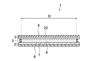
- FIG. 1 is a plan view showing an overall configuration of a liquid crystal display device according to a first embodiment of the present invention.
- FIG. 2 is a cross-sectional view taken along the line AA in FIG. It is the top view to which the pixel part of the TFT substrate which concerns on the 1st Embodiment of this invention was expanded.
- It is sectional drawing which shows the whole structure of the TFT substrate which comprises the liquid crystal display device which concerns on the 1st Embodiment of this invention.
- It is sectional drawing which shows the whole structure of the display part of the liquid crystal display device which concerns on the 1st Embodiment of this invention.
- It is a perspective view which shows the state which bent the TFT substrate which concerns on the 1st Embodiment of this invention.
- FIG. 4 is a sectional view taken along line BB in FIG. 3. It is a top view for demonstrating arrangement
- FIG. 1 is a plan view showing an overall configuration of a liquid crystal display device according to a first embodiment of the present invention
- FIG. 2 is a cross-sectional view taken along the line AA in FIG. 3 is an enlarged plan view of the pixel portion of the TFT substrate according to the first embodiment of the present invention
- FIG. 4 is a TFT constituting the liquid crystal display device according to the first embodiment of the present invention.
- It is sectional drawing which shows the whole structure of a board
- FIG. 5 is a cross-sectional view showing the overall configuration of the display unit of the liquid crystal display device according to the first embodiment of the present invention
- FIG. 6 shows a bent TFT substrate according to the first embodiment of the present invention. It is a perspective view which shows the state which carried out.
- FIG. 7 is a sectional view taken along line BB in FIG.
- a liquid crystal display device will be described as an example of the display device.
- the liquid crystal display device 1 includes a TFT substrate 2 that is a display device substrate on which a plurality of TFTs (Thin-FilmTransistors) that are switching elements are formed, and a TFT substrate 2 facing the TFT substrate 2. And a CF substrate 3 which is another display device substrate. Further, the liquid crystal display device 1 is sandwiched between a liquid crystal layer 4 which is a display medium layer sandwiched between the TFT substrate 2 and the CF substrate 3, and the TFT substrate 2 and the CF substrate 3. The substrate 2 and the CF substrate 3 are bonded to each other, and a sealing material 5 provided in a frame shape is provided to enclose the liquid crystal layer 4.
- TFT substrate 2 that is a display device substrate on which a plurality of TFTs (Thin-FilmTransistors) that are switching elements are formed
- a CF substrate 3 which is another display device substrate.
- the liquid crystal display device 1 is sandwiched between a liquid crystal layer 4
- the sealing material 5 is formed so as to circulate around the liquid crystal layer 4, and the TFT substrate 2 and the CF substrate 3 are bonded to each other via the sealing material 5.
- the TFT substrate 2 and the CF substrate 3 are each formed in a rectangular plate shape.
- the liquid crystal display device 1 includes a plurality of photo spacers (not shown) for regulating the thickness of the liquid crystal layer 4 (that is, the cell gap).
- a display area D for image display is defined in an area where the TFT substrate 2 and the CF substrate 3 overlap inside the sealing material 5. Yes.
- the display area D includes a plurality of pixels E (see FIGS. 3 and 8), which are the minimum unit of an image, arranged in a matrix.
- the liquid crystal display device 1 is formed in a rectangular shape, and in the longitudinal direction of the liquid crystal display device 1, the TFT substrate 2 protrudes from the CF substrate 3 on the upper side thereof.
- a terminal region T is defined in the protruding region.
- the terminal area T is provided around the display area D as shown in FIG.
- the terminal region T is provided with a plurality of terminals (not shown) and connection wiring (not shown) connected to each of the plurality of terminals.
- the TFT substrate 2 includes a substrate 6 having film-like flexibility (flexibility).
- a substrate 6 having film-like flexibility (flexibility) for example, a plastic substrate formed of an organic material such as polyimide resin, polyparaxylene resin, or acrylic resin can be used. Note that a metal substrate having flexibility may be used instead of the plastic substrate.
- a display element layer 7 provided with TFTs and the like is formed on the substrate 6 of the TFT substrate 2.
- the display element layer 7 includes a base coat layer 9 provided on the substrate 6, a plurality of gate wirings 11 extending in parallel to each other on the base coat layer 9, and And a gate insulating film 12 provided so as to cover each gate wiring 11.
- the display element layer 7 includes a plurality of source lines 14 extending in parallel with each other in a direction orthogonal to the gate lines 11 on the gate insulating film 12, and each intersection of the gate lines 11 and the source lines 14.
- a plurality of TFT elements 15 are provided, and a plurality of auxiliary capacitance lines 16 are provided between the gate lines 11 and extend in parallel to each other.
- the display element layer 7 is provided in a matrix on the interlayer insulating film 10 provided on the interlayer insulating film 10 so as to cover each gate wiring 11, each source wiring 14, and each TFT element 15.
- a plurality of pixel electrodes 19 connected to each of the elements 15 and an alignment film 20 provided so as to cover each pixel electrode 19 are provided.
- the TFT element 15 includes a gate electrode 27 in which each gate wiring 11 protrudes to the side, a gate insulating film 12 provided so as to cover the gate electrode 27, and the gate insulating film 12.
- the semiconductor layer 23 is provided in an island shape at a position overlapping the gate electrode 27, and the source electrode 28 and the drain electrode 29 are provided so as to face each other on the semiconductor layer 23.
- the source electrode 28 is a portion where each source wiring 14 protrudes to the side.
- the drain electrode 29 is connected to the pixel electrode 19 through a contact hole 30 formed in the interlayer insulating film 10 as shown in FIG.
- the pixel electrode 19 includes a transparent electrode 31 provided on the interlayer insulating film 10, and a reflective electrode 32 stacked on the transparent electrode 31 and provided on the surface of the transparent electrode 31. It is comprised by.
- the semiconductor layer 23 includes a lower intrinsic amorphous silicon layer 23 a and an upper n + amorphous silicon layer 23 b doped with phosphorus, and is exposed from the source electrode 28 and the drain electrode 29.
- the intrinsic amorphous silicon layer 23a that constitutes the channel region.
- drain electrode 29 forms an auxiliary capacitance by overlapping with the auxiliary capacitance wiring 16 through the gate insulating film 12.
- the material constituting the base coat layer 9 examples include materials such as silicon oxide (SiO 2 ), silicon nitride (SiNx (x is a positive number)), silicon oxynitride (SiNO), and the like. Note that the base coat layer 9 may have a laminated structure of these materials.
- the material constituting the gate insulating film 12 is not particularly limited.
- silicon oxide (SiO 2 ) a material having a lower dielectric constant than silicon oxide such as SiOF, SiOC, or the like, trisilicon tetranitride (Si 3 N 4 ) silicon nitride such as (SiNx (x is a positive number)), silicon oxynitride (SiNO), titanium dioxide (TiO 2), dialuminum trioxide (Al 2 O 3), tantalum pentoxide (Ta 2 O 5 ) And other materials having a higher dielectric constant than silicon oxide such as hafnium dioxide (HfO 2 ) and zirconium dioxide (ZrO 2 ).
- the gate insulating film 12 may have a single-layer structure or a stacked structure.
- the material constituting the interlayer insulating film 10 is not particularly limited, and examples thereof include insulating materials such as silicon oxide (SiO 2 ) and silicon nitride (SiNx (x is a positive number)).
- the CF substrate 3 includes a substrate 8 having a film-like flexibility (flexibility) formed of a resin material, like the TFT substrate 2.
- a resin material like the TFT substrate 2.
- a plastic substrate formed of an organic material such as polyimide resin, polyparaxylene resin, or acrylic resin can be used.
- a metal substrate having flexibility may be used instead of the plastic substrate.
- a CF element layer 22 is formed on the substrate 8 of the CF substrate 3.
- the CF element layer 22 includes a color filter 48 provided on the substrate 8, a common electrode 24 provided so as to cover the reflective region of the color filter 48, and the common electrode 24.
- a photo spacer (not shown) provided in a column shape, and an alignment film 26 provided so as to cover the common electrode 24 and the photo spacer.
- the color filter 48 includes a plurality of types of colored layers 39 (that is, a red layer, a green layer, and a blue layer) provided for each pixel, and a black matrix that is a light shielding film. 36.
- the black matrix 36 is provided between adjacent colored layers 39 and has a role of partitioning these plural types of colored layers 39.
- the black matrix 36 is made of a metal material such as Ta (tantalum), Cr (chromium), Mo (molybdenum), Ni (nickel), Ti (titanium), Cu (copper), Al (aluminum), or a black pigment such as carbon.
- a metal material such as Ta (tantalum), Cr (chromium), Mo (molybdenum), Ni (nickel), Ti (titanium), Cu (copper), Al (aluminum), or a black pigment such as carbon.
- the photo spacer is made of, for example, an acrylic photosensitive resin, and is formed by a photolithography method.
- the thickness of the substrates 6 and 8 is preferably 3 to 30 ⁇ m. When the thickness is less than 3 ⁇ m, sufficient mechanical strength may not be obtained. When the thickness is greater than 30 ⁇ m, the substrate 6 is formed when the display element layer 7 and the CF element layer 22 are formed. , 8 becomes large and a problem may occur in the process.
- the liquid crystal layer 4 includes, for example, nematic liquid crystal having electro-optical characteristics.
- a reflection region R is defined by the reflection electrode 32 as shown in FIG. Further, the surface of the interlayer insulating film 10 under the pixel electrode 19 is formed in an uneven shape, and the surface of the reflective electrode 32 provided on the surface of the interlayer insulating film 10 via the transparent electrode 31 is also formed in an uneven shape. Has been.
- a liquid crystal display including a pixel electrode 19, a liquid crystal layer 4 formed on the pixel electrode 19, and a common electrode 24 formed on the liquid crystal layer 4 on the TFT substrate 2.
- An element 35 is provided.
- a polarizing plate (not shown) is provided outside the substrate 6 of the TFT substrate 2, and a backlight unit (not shown) is provided outside the polarizing plate.
- a polarizing plate (not shown) is provided outside the substrate 8 of the CF substrate 3.
- the reflective liquid crystal display device 1 having the above-described configuration is configured such that light incident from the CF substrate 3 side in the reflective region R is reflected by the reflective electrode 32.
- one pixel E is configured for each pixel electrode 19, and in each pixel E, when a gate signal is sent from the gate wiring 11 and the TFT element 15 is turned on, A source signal is sent from the source wiring 14 and a predetermined charge is written to the pixel electrode 19 through the source electrode 28 and the drain electrode 29, and a potential difference is generated between the pixel electrode 19 and the common electrode 24, and the liquid crystal layer 4 Is configured to be applied with a predetermined voltage.
- the reflectance of light incident from the CF substrate 3 side is adjusted using the fact that the alignment state of the liquid crystal molecules changes according to the magnitude of the applied voltage. Is displayed.
- a plurality of trench grooves 25 are provided in the vicinity of the TFT element 15 and the wiring (that is, the gate wiring 11 and the source wiring 14). There is a feature in that.
- the TFT substrate 2 is bent at the portion of the trench groove 25 that is resistant to stress as shown in FIG. Therefore, stress concentrates in the trench groove 25. Accordingly, a portion that is vulnerable to stress, for example, a crossing portion (wiring crossing portion) 33 of the gate wiring 11 and the source wiring 14 shown in FIG. 3 or a step portion in the TFT element 15 (that is, a step portion of the source electrode 28 or the drain electrode 29). ) It is possible to avoid the concentration of stress on 34, so that the disconnection of the wiring (that is, the gate wiring 11 and the source wiring 14) due to the bending and the damage to the TFT element 15 can be suppressed.
- a crossing portion (wiring crossing portion) 33 of the gate wiring 11 and the source wiring 14 shown in FIG. 3 or a step portion in the TFT element 15 that is, a step portion of the source electrode 28 or the drain electrode 29.
- the trench groove 25 is formed in the insulating film (that is, the gate insulating film 12 and the interlayer insulating film 10), and the pixel electrode 19 is provided on the surface of the trench groove 25. It has become.
- the trench groove 25 is formed along the gate line 11 and the source line 14. It is preferable to do.
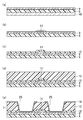
- FIG. 9 is a cross-sectional view for explaining a manufacturing method of the TFT substrate in the liquid crystal display device according to the first embodiment of the present invention, and more particularly, a diagram showing a manufacturing process of the TFT element.
- FIG. 10 is a cross-sectional view for explaining a method of manufacturing a TFT substrate in the liquid crystal display device according to the first embodiment of the present invention, and particularly shows a manufacturing process of a trench groove.
- FIG. 11 is a cross-sectional view for explaining the method for manufacturing the CF substrate in the liquid crystal display device according to the first embodiment of the present invention.
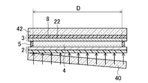
- FIGS. 12 to 14 are cross-sectional views for explaining the manufacturing method of the liquid crystal display device according to the first embodiment of the present invention.
- the manufacturing method shown below is a mere illustration, and the liquid crystal display device 1 which concerns on this invention is not limited to what was manufactured by the method shown below.
- ⁇ TFT substrate manufacturing process> Glass substrate preparation process
- a glass substrate 40 having a thickness of about 0.7 mm is prepared as a support substrate.
- a film-like flexible substrate 6 formed of, for example, a polyimide resin is formed on a glass substrate 40 with a thickness of, for example, about 20 ⁇ m. Form with.
- the substrate 6 may be formed by applying an organic material such as polyimide resin on the glass substrate 40.
- a base coat layer 9 made of, for example, silicon oxide (or silicon nitride) is formed on the substrate 6 by a method such as a CVD method.
- the molybdenum film having a single layer structure is exemplified as the metal film constituting the gate electrode 27.
- a metal such as an aluminum film, a tungsten film, a tantalum film, a chromium film, a titanium film, or a copper film is used.
- the gate electrode 27 may be formed with a thickness of 50 nm to 300 nm using a film, or an alloy film or a metal nitride film thereof.
- a silicon nitride film (thickness of about 200 nm to 500 nm) is formed by CVD on the entire substrate on which the gate wiring 11, the gate electrode 27, and the auxiliary capacitance wiring 16 are formed, and FIG. As shown in FIG. 10C, the gate insulating film 12 is formed so as to cover the gate wiring 11, the gate electrode 27, and the auxiliary capacitance wiring 16. Note that the gate insulating film 12 may have a two-layer structure.
- an intrinsic amorphous silicon film (thickness of about 2000 mm) and phosphorus-doped n + amorphous silicon film (thickness of about 500 mm) are formed on the entire substrate on which the gate insulating film 12 is formed by plasma CVD. Films are continuously formed. Thereafter, the semiconductor electrode is patterned on the gate electrode 27 by photolithography to form a semiconductor formation layer in which the intrinsic amorphous silicon layer 23a and the n + amorphous silicon layer 23b are stacked.
- an aluminum film and a titanium film are sequentially formed on the entire substrate on which the semiconductor formation layer has been formed by sputtering, and then patterned by photolithography to form the source wiring 14, the source electrode 28, and the drain.
- the electrode 29 is formed to a thickness of about 2000 mm.
- the n + amorphous silicon layer 23b of the semiconductor formation layer is etched by using the source electrode 28 and the drain electrode 29 as a mask to pattern the channel region, and as shown in FIG. A TFT element 15 having the same is formed.
- a silicon oxide film is formed by plasma CVD on the entire substrate on which the source electrode 28 and the drain electrode 29 are formed (that is, the TFT element 15 is formed), and FIG.
- the interlayer insulating film 10 covering the TFT element 15 is formed to a thickness of about 265 nm, for example. To do.
- a photomask having a predetermined pattern is formed on the interlayer insulating film 10 by photolithography.
- exposure and development are performed using this photomask, and patterning is performed using an etching method, whereby the interlayer insulating film 10 is etched as shown in FIG. 30 is formed, and as shown in FIG. 10E, the interlayer insulating film 10 and the gate insulating film 12 are etched to form a trench groove 25.
- the trench groove 25 in the formation of the contact hole, can be formed simultaneously with the contact hole 30 only by changing the design of the photomask that has been conventionally used.
- the trench groove 25 can be formed without any problem.
- the gate insulating film 12 and the interlayer insulating film 10 are formed of a photosensitive resin (for example, acrylic photosensitive resin), and a halftone mask or a gray tone mask is used as a photomask to perform exposure processing (halftone).
- the trench groove 25 may be formed by controlling the exposure amount irradiated to the photosensitive resin by performing an exposure process or a gray tone exposure process. Further, the trench groove 25 can be formed by pressing a convex mold or the like against the gate insulating film 12 and the interlayer insulating film 10.
- a transparent conductive film such as an ITO film (thickness of about 50 nm to 200 nm) made of indium tin oxide is formed on the entire substrate on which the interlayer insulating film 10 is formed by sputtering, and then the transparent conductive film By performing photolithography, wet etching, and resist peeling and cleaning on the film, the pixel electrode 19 is formed as shown in FIGS. 9F and 10E.
- the pixel electrode 19 has the surfaces of the interlayer insulating film 10 and the gate insulating film 12 so as to cover the surfaces of the trench groove 25 and the contact hole 30. Formed on top.
- a polyimide resin is applied to the entire substrate by a printing method, and then a rubbing process is performed to form the alignment film 20.
- a photo spacer made of an acrylic photosensitive resin is formed on the entire substrate by using, for example, a photolithography method.
- the TFT substrate 2 in which the display element layer 7 including the TFT elements 15 and the trench grooves 25 is formed on the substrate 6 can be manufactured.
- a glass substrate 42 having a thickness of about 0.7 mm is prepared as a support substrate.
- a film-like flexible substrate 8 made of, for example, a polyimide resin is formed on the glass substrate 42 with a thickness of about 20 ⁇ m, for example.
- the color filter 48 including the colored layer 39 and the black matrix 36 is formed on the substrate 8, and the common electrode 24 and the like are patterned to form the CF element layer 22. Thereafter, a polyimide resin is applied to the entire substrate by a printing method, and then a rubbing process is performed to form an alignment film 26, whereby the CF substrate 3 constituting the display region D is manufactured.
- ⁇ TFT substrate / CF substrate bonding process First, for example, using a dispenser, the sealing material 5 made of ultraviolet curing and thermosetting resin or the like is drawn on the CF substrate 3 in a frame shape.
- a liquid crystal material for forming the liquid crystal layer 4 is dropped on a region inside the sealing material 5 in the CF substrate 3 on which the sealing material 5 is drawn.
- the CF substrate 3 onto which the liquid crystal material is dropped and the TFT substrate 2 are bonded together under reduced pressure.
- the front and back surfaces of the bonded body are pressurized by releasing the bonded body to atmospheric pressure. Then, after irradiating the sealing material 5 sandwiched between the bonded bodies with UV light, the sealing material 5 is cured by heating the bonded body, and as shown in FIG. 12, the TFT substrate 2 and the CF substrate 3 A bonded body in which is bonded is produced.
- the glass substrate 40 is peeled off by irradiating laser light (arrows in FIG. 13) from the glass substrate 40 side.
- the removal of the glass substrate 40 may not be peeling by laser light irradiation.
- the glass substrate 40 may be removed using a polishing or etching apparatus.
- the glass substrate 42 is peeled off by irradiating laser light (arrows in FIG. 14) from the glass substrate 42 side.
- the removal of the glass substrate 42 may not be peeling by laser light irradiation, as in the case of the glass substrate 40 described above.
- the glass substrate 42 may be removed using a polishing or etching apparatus.
- a polarizing plate (not shown) and a backlight unit (not shown) are provided to complete the liquid crystal display device 1 shown in FIG.
- the trench groove 25 is provided in the vicinity of the TFT element 15 and the wiring (gate wiring 11 and source wiring 14). Accordingly, even when an external force is applied to the TFT substrate 2, the TFT substrate 2 bends at the portion of the trench groove 25 that is resistant to stress, so that the stress is concentrated in the trench groove 25. Accordingly, concentration of stress on the wiring (gate wiring 11 and source wiring 14) and the TFT element 15 that are vulnerable to stress can be avoided, and therefore, disconnection of wiring due to bending and damage to the TFT element 15 can be suppressed. Can do. As a result, the yield of the TFT substrate 2 can be improved.
- a plurality of trench grooves 25 are provided. Therefore, since it is possible to further avoid stress concentration on the wiring and the TFT element 15 which are vulnerable to stress, it is possible to further suppress the disconnection of the wiring and the damage to the TFT element 15 caused by bending.
- the trench groove 25 is formed along the gate wiring 11 and the source wiring 14. Therefore, in particular, stress concentration on the gate wiring 11 and the source wiring 14 can be further avoided, so that disconnection of the gate wiring 11 and the source wiring 14 due to bending can be further suppressed.
- the trench groove 25 is provided at the periphery of each of the plurality of pixels E. Therefore, the trench groove 25 can be provided without considering the influence on the image display.
- the trench groove 25 is formed in the insulating film (that is, the gate insulating film 12 and the interlayer insulating film 10). Therefore, it is possible to provide a device resistant to stress by simple trench formation.
- FIG. 15 is a cross-sectional view showing a trench formed in the TFT substrate according to the second embodiment of the present invention. Note that the same components as those in the first embodiment are denoted by the same reference numerals, and description thereof is omitted. Further, the overall configuration of the liquid crystal display device is the same as that described in the first embodiment, and therefore detailed description thereof is omitted here.
- the trench groove 25 is formed in the gate insulating film 12 and the interlayer insulating film 10 as shown in FIG. 7, but in this embodiment, as shown in FIG. A feature is that a trench groove 38 is formed in the gate insulating film 12 and the interlayer insulating film 10.
- the trench groove 38 has a depth greater than that of the trench groove 25 described above. Therefore, when an external force such as mechanical stress acts on the TFT substrate 2, the trench groove resistant to stress.
- the liquid crystal display device 1 is easily bent at the portion 38, and stress is further concentrated in the trench groove 38. Therefore, it is possible to further avoid stress concentration on the intersection 33 of the gate wiring 11 and the source wiring 14 and the step portion 34 of the source electrode 28 and the drain electrode in the TFT element 15, which is weak against stress. The disconnection of the wiring to be performed and the damage to the TFT element 15 can be further suppressed.
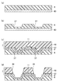
- FIG. 16 is a diagram showing a manufacturing process of a trench groove according to the second embodiment of the present invention.
- the TFT element manufacturing process, the CF substrate manufacturing process, and the TFT substrate / CF substrate bonding process are the same as those described in the first embodiment, and a detailed description thereof is omitted here.
- the glass substrate 40 about 0.7 mm thick is prepared as a support substrate, for example.
- a film-like flexible substrate 6 formed of, for example, a polyimide resin is formed on the glass substrate 40 with a thickness of about 20 ⁇ m, for example.
- a photoresist is formed on the substrate 6 by photolithography, and the photoresist is ashed to remove a portion corresponding to the trench groove of the photoresist. Then, using this photoresist as a photomask, patterning is performed using an etching method, thereby forming a groove 37 to be a part of the trench groove 38 in the substrate 6 as shown in FIG. .
- the base coat layer 9, the gate wiring 11, the gate insulating film 12, and the interlayer insulating film 10 are formed.
- the base coat layer 9 is formed on the surface of the substrate 6 so as to cover the surface of the groove 37.
- a photomask having a predetermined pattern is formed by photolithography, exposure and development are performed using this photomask, and patterning is performed using an etching method.
- the interlayer insulating film 10 and the gate insulating film 12 are etched to form a trench groove 38.
- the interlayer insulating film 10 is etched to form the contact hole 30.
- the pixel electrode 19 is formed, and the alignment film 20 and the spacer are formed, whereby the TFT substrate 2 in which the display element layer 7 is formed on the substrate 6 is manufactured. can do.
- the trench groove 38 is formed in the substrate 6 and the insulating film (that is, the gate insulating film 12 and the interlayer insulating film 10). Accordingly, it is possible to form the trench groove 38 that is resistant to stress with a simple configuration. Further, since the trench groove 38 having a large depth can be formed, the TFT substrate 2 is easily bent at the trench groove 38, and stress can be further concentrated in the trench groove 38. Therefore, stress concentration on the wiring and the TFT element 15 that is vulnerable to stress can be further avoided, and thus disconnection of the wiring due to bending and damage to the TFT element 15 can be further suppressed.
- the trench groove 25 is formed in the gate insulating film 12 and the interlayer insulating film 10.
- a trench groove may be formed only in the upper interlayer insulating film 10.
- trench grooves 25 and 38 described above may be provided close to the auxiliary capacitance wiring 16.
- an LCD liquid crystal display
- the display device is not limited to this, and a TFT element is formed on a flexible substrate. Any display device may be used as long as it includes a display device substrate having a display element layer on which wiring is formed.
- organic EL organic electroluminescence
- electrophoresis electrophoretic
- PD plasma display
- PALC plasma addressed liquid crystal display
- inorganic EL inorganic electroluminescence
- FED field It may be a display device related to emission S display (field emission display) or SED (surface-conduction electron-emitter display).
- the semiconductor layer 23 has been described by taking an example of amorphous silicon.
- a semiconductor layer made of polysilicon or continuous grain boundary crystal (CG) silicon may be used.
- CG continuous grain boundary crystal
- IGZO indium gallium zinc oxide
- the present invention is particularly useful for a display device substrate including a plastic substrate and a display device including the same.
- Liquid crystal display device 2 TFT substrate (display device substrate) 3 CF substrate 4 Liquid crystal layer 6 Substrate 7 Display element layer 8 Substrate 10 Interlayer insulating film (insulating film) 11 Gate wiring (wiring) 12 Gate insulating film (insulating film) 14 Source wiring (wiring) 15 TFT element (switching element) 16 Auxiliary Capacitor Line 19 Pixel Electrode 22 CF Element Layer 23 Semiconductor Layer 24 Common Electrode 25 Trench Groove 27 Gate Electrode 28 Source Electrode 29 Drain Electrode 30 Contact Hole 33 Intersection of Gate Line and Source Line 34 Stepped Part 35 in TFT Element 35 Liquid Crystal Display Element (display element) 38 trench groove 40 glass substrate 42 glass substrate 48 color filter
Landscapes
- Liquid Crystal (AREA)
- Devices For Indicating Variable Information By Combining Individual Elements (AREA)
Abstract
L'invention concerne un substrat de transistor en couche mince (3) comprenant : un substrat souple ; une couche élément d'affichage formée sur le substrat et pourvue d'un élément transistor en couche mince (15), d'un câblage de grille (11) et d'un câblage de source (14) ; et des rainures en tranchées (25) formées à proximité de l'élément transistor en couche mince (15), du câblage de grille (11) et du câblage de source (14).
Applications Claiming Priority (2)
| Application Number | Priority Date | Filing Date | Title |
|---|---|---|---|
| JP2011122433 | 2011-05-31 | ||
| JP2011-122433 | 2011-05-31 |
Publications (1)
| Publication Number | Publication Date |
|---|---|
| WO2012164882A1 true WO2012164882A1 (fr) | 2012-12-06 |
Family
ID=47258759
Family Applications (1)
| Application Number | Title | Priority Date | Filing Date |
|---|---|---|---|
| PCT/JP2012/003399 Ceased WO2012164882A1 (fr) | 2011-05-31 | 2012-05-24 | Substrat pour dispositif d'affichage et dispositif d'affichage le comprenant |
Country Status (1)
| Country | Link |
|---|---|
| WO (1) | WO2012164882A1 (fr) |
Cited By (6)
| Publication number | Priority date | Publication date | Assignee | Title |
|---|---|---|---|---|
| JP2015002177A (ja) * | 2013-06-17 | 2015-01-05 | 三星ディスプレイ株式會社Samsung Display Co.,Ltd. | アレイ基板及びこれを含む有機発光表示装置 |
| CN104297959A (zh) * | 2014-10-17 | 2015-01-21 | 深圳市华星光电技术有限公司 | 液晶显示器 |
| KR20150037159A (ko) * | 2013-09-30 | 2015-04-08 | 엘지디스플레이 주식회사 | 플렉서블 표시장치 및 그 제조 방법 |
| JP2017134329A (ja) * | 2016-01-29 | 2017-08-03 | 株式会社 オルタステクノロジー | 液晶表示装置及びその製造方法 |
| JP2018518043A (ja) * | 2015-04-13 | 2018-07-05 | ロイヨール コーポレーション | 可撓性基板の支持及び取り外し |
| CN108461393A (zh) * | 2018-05-07 | 2018-08-28 | 京东方科技集团股份有限公司 | 显示基板的制备方法、显示基板及显示装置 |
Citations (5)
| Publication number | Priority date | Publication date | Assignee | Title |
|---|---|---|---|---|
| JP2004519866A (ja) * | 2001-04-03 | 2004-07-02 | コーニンクレッカ フィリップス エレクトロニクス エヌ ヴィ | フレキシブルな基板を有するマトリクスアレイデバイス |
| JP2004531753A (ja) * | 2001-02-16 | 2004-10-14 | イグニス イノベーション インコーポレーテッド | 可撓性表示装置 |
| JP2006270077A (ja) * | 2005-02-25 | 2006-10-05 | Semiconductor Energy Lab Co Ltd | 半導体装置およびその作製方法 |
| JP2008542834A (ja) * | 2005-05-31 | 2008-11-27 | コーニンクレッカ フィリップス エレクトロニクス エヌ ヴィ | 柔軟なディスプレイデバイス |
| JP2010072380A (ja) * | 2008-09-19 | 2010-04-02 | Hitachi Displays Ltd | 表示装置 |
-
2012
- 2012-05-24 WO PCT/JP2012/003399 patent/WO2012164882A1/fr not_active Ceased
Patent Citations (5)
| Publication number | Priority date | Publication date | Assignee | Title |
|---|---|---|---|---|
| JP2004531753A (ja) * | 2001-02-16 | 2004-10-14 | イグニス イノベーション インコーポレーテッド | 可撓性表示装置 |
| JP2004519866A (ja) * | 2001-04-03 | 2004-07-02 | コーニンクレッカ フィリップス エレクトロニクス エヌ ヴィ | フレキシブルな基板を有するマトリクスアレイデバイス |
| JP2006270077A (ja) * | 2005-02-25 | 2006-10-05 | Semiconductor Energy Lab Co Ltd | 半導体装置およびその作製方法 |
| JP2008542834A (ja) * | 2005-05-31 | 2008-11-27 | コーニンクレッカ フィリップス エレクトロニクス エヌ ヴィ | 柔軟なディスプレイデバイス |
| JP2010072380A (ja) * | 2008-09-19 | 2010-04-02 | Hitachi Displays Ltd | 表示装置 |
Cited By (23)
| Publication number | Priority date | Publication date | Assignee | Title |
|---|---|---|---|---|
| US11264408B2 (en) | 2013-06-17 | 2022-03-01 | Samsung Display Co., Ltd. | Array substrate and organic light-emitting display including the same |
| US11916087B2 (en) | 2013-06-17 | 2024-02-27 | Samsung Display Co., Ltd. | Array substrate and organic light-emitting display including the same |
| EP2816604A3 (fr) * | 2013-06-17 | 2015-03-11 | Samsung Display Co., Ltd. | Substrat de réseau et affichage électroluminescent organique l'incluant |
| JP2015002177A (ja) * | 2013-06-17 | 2015-01-05 | 三星ディスプレイ株式會社Samsung Display Co.,Ltd. | アレイ基板及びこれを含む有機発光表示装置 |
| US9472507B2 (en) | 2013-06-17 | 2016-10-18 | Samsung Display Co., Ltd. | Array substrate and organic light-emitting display including the same |
| CN109378319B (zh) * | 2013-06-17 | 2023-10-24 | 三星显示有限公司 | 阵列衬底 |
| CN109378319A (zh) * | 2013-06-17 | 2019-02-22 | 三星显示有限公司 | 阵列衬底 |
| EP3879581A1 (fr) * | 2013-06-17 | 2021-09-15 | Samsung Display Co., Ltd. | Substrat de réseau et affichage électroluminescent organique l'incluant |
| US10553619B2 (en) | 2013-06-17 | 2020-02-04 | Samsung Display Co., Ltd. | Array substrate and organic light-emitting display including the same |
| KR20150037159A (ko) * | 2013-09-30 | 2015-04-08 | 엘지디스플레이 주식회사 | 플렉서블 표시장치 및 그 제조 방법 |
| CN104518000A (zh) * | 2013-09-30 | 2015-04-15 | 乐金显示有限公司 | 柔性显示设备及其制造方法 |
| CN104518000B (zh) * | 2013-09-30 | 2017-07-11 | 乐金显示有限公司 | 柔性显示设备及其制造方法 |
| KR102052686B1 (ko) | 2013-09-30 | 2019-12-05 | 엘지디스플레이 주식회사 | 플렉서블 표시장치 및 그 제조 방법 |
| WO2016058260A1 (fr) * | 2014-10-17 | 2016-04-21 | 深圳市华星光电技术有限公司 | Affichage à cristaux liquides |
| CN104297959B (zh) * | 2014-10-17 | 2018-08-07 | 深圳市华星光电技术有限公司 | 液晶显示器 |
| CN104297959A (zh) * | 2014-10-17 | 2015-01-21 | 深圳市华星光电技术有限公司 | 液晶显示器 |
| US10529924B2 (en) | 2015-04-13 | 2020-01-07 | Shenzhen Royole Technologies Co. Ltd. | Support and detachment of flexible substrates |
| JP2018518043A (ja) * | 2015-04-13 | 2018-07-05 | ロイヨール コーポレーション | 可撓性基板の支持及び取り外し |
| CN108496110A (zh) * | 2016-01-29 | 2018-09-04 | 奥特司科技株式会社 | 液晶显示装置及其制造方法 |
| WO2017130950A1 (fr) * | 2016-01-29 | 2017-08-03 | 株式会社オルタステクノロジー | Dispositif d'affichage à cristaux liquides, et son procédé de fabrication |
| JP2017134329A (ja) * | 2016-01-29 | 2017-08-03 | 株式会社 オルタステクノロジー | 液晶表示装置及びその製造方法 |
| CN108461393A (zh) * | 2018-05-07 | 2018-08-28 | 京东方科技集团股份有限公司 | 显示基板的制备方法、显示基板及显示装置 |
| CN108461393B (zh) * | 2018-05-07 | 2021-03-16 | 京东方科技集团股份有限公司 | 显示基板的制备方法、显示基板及显示装置 |
Similar Documents
| Publication | Publication Date | Title |
|---|---|---|
| KR101225440B1 (ko) | 액정 표시 장치 및 그 제조 방법 | |
| US20130023086A1 (en) | Active matrix substrate, display panel provided with same, and method for manufacturing active matrix substrate | |
| CN100562989C (zh) | 液晶显示器件及其制造方法 | |
| CN102667597B (zh) | 有源矩阵基板和显示装置 | |
| WO2012063436A1 (fr) | Substrat pour dispositif d'affichage, son procédé de production, et dispositif d'affichage | |
| WO2011004521A1 (fr) | Panneau d'affichage | |
| WO2012164882A1 (fr) | Substrat pour dispositif d'affichage et dispositif d'affichage le comprenant | |
| KR20090088575A (ko) | 박막 트랜지스터 기판의 제조 방법 | |
| JP2009042292A (ja) | 液晶表示装置 | |
| KR20110040222A (ko) | 프린지 필드형 액정표시장치 및 그 제조방법 | |
| WO2013171989A1 (fr) | Substrat à réseau et panneau d'affichage à cristaux liquides comprenant celui-ci | |
| US9224824B2 (en) | Display device substrate and display device equipped with same | |
| KR20130015245A (ko) | 프린지 필드형 액정표시장치 및 그 제조방법 | |
| JP4564473B2 (ja) | 液晶表示装置の製造方法 | |
| KR102484136B1 (ko) | 표시 기판, 이를 포함하는 액정 표시 장치, 및 이의 제조 방법 | |
| US20120081273A1 (en) | Pixel structure, pixel array and display panel | |
| JP2007013083A (ja) | 薄膜トランジスタ基板及びその製造方法 | |
| US20120069260A1 (en) | Active matrix substrate, liquid crystal display device including the same, and method for fabricating active matrix substrate | |
| CN100485470C (zh) | 液晶显示器及其制造方法 | |
| KR102084397B1 (ko) | 액정표시장치의 제조방법 | |
| WO2012049824A1 (fr) | Substrat de transistor à couches minces, et dispositif d'affichage mettant en oeuvre celui-ci | |
| WO2012077586A1 (fr) | Substrat de réseau pour écran d'affichage à cristaux liquides | |
| WO2010079706A1 (fr) | Substrat de réseau pour panneau à cristaux liquides, et dispositif d'affichage à cristaux liquides comprenant le substrat | |
| US20130071792A1 (en) | Method for fabricating liquid crystal display device | |
| WO2013014885A1 (fr) | Substrat à matrice active et panneau d'affichage à cristaux liquides utilisant celui-ci |
Legal Events
| Date | Code | Title | Description |
|---|---|---|---|
| 121 | Ep: the epo has been informed by wipo that ep was designated in this application |
Ref document number: 12793028 Country of ref document: EP Kind code of ref document: A1 |
|
| NENP | Non-entry into the national phase |
Ref country code: DE |
|
| 122 | Ep: pct application non-entry in european phase |
Ref document number: 12793028 Country of ref document: EP Kind code of ref document: A1 |
|
| NENP | Non-entry into the national phase |
Ref country code: JP |