WO2012164882A1 - 表示装置用基板およびそれを備えた表示装置 - Google Patents
表示装置用基板およびそれを備えた表示装置 Download PDFInfo
- Publication number
- WO2012164882A1 WO2012164882A1 PCT/JP2012/003399 JP2012003399W WO2012164882A1 WO 2012164882 A1 WO2012164882 A1 WO 2012164882A1 JP 2012003399 W JP2012003399 W JP 2012003399W WO 2012164882 A1 WO2012164882 A1 WO 2012164882A1
- Authority
- WO
- WIPO (PCT)
- Prior art keywords
- substrate
- display device
- wiring
- insulating film
- tft
- Prior art date
- Legal status (The legal status is an assumption and is not a legal conclusion. Google has not performed a legal analysis and makes no representation as to the accuracy of the status listed.)
- Ceased
Links
Images


Classifications
-
- H—ELECTRICITY
- H10—SEMICONDUCTOR DEVICES; ELECTRIC SOLID-STATE DEVICES NOT OTHERWISE PROVIDED FOR
- H10D—INORGANIC ELECTRIC SEMICONDUCTOR DEVICES
- H10D86/00—Integrated devices formed in or on insulating or conducting substrates, e.g. formed in silicon-on-insulator [SOI] substrates or on stainless steel or glass substrates
- H10D86/40—Integrated devices formed in or on insulating or conducting substrates, e.g. formed in silicon-on-insulator [SOI] substrates or on stainless steel or glass substrates characterised by multiple TFTs
- H10D86/411—Integrated devices formed in or on insulating or conducting substrates, e.g. formed in silicon-on-insulator [SOI] substrates or on stainless steel or glass substrates characterised by multiple TFTs characterised by materials, geometry or structure of the substrates
-
- H—ELECTRICITY
- H10—SEMICONDUCTOR DEVICES; ELECTRIC SOLID-STATE DEVICES NOT OTHERWISE PROVIDED FOR
- H10D—INORGANIC ELECTRIC SEMICONDUCTOR DEVICES
- H10D30/00—Field-effect transistors [FET]
- H10D30/60—Insulated-gate field-effect transistors [IGFET]
- H10D30/67—Thin-film transistors [TFT]
- H10D30/6758—Thin-film transistors [TFT] characterised by the insulating substrates
-
- H—ELECTRICITY
- H10—SEMICONDUCTOR DEVICES; ELECTRIC SOLID-STATE DEVICES NOT OTHERWISE PROVIDED FOR
- H10D—INORGANIC ELECTRIC SEMICONDUCTOR DEVICES
- H10D86/00—Integrated devices formed in or on insulating or conducting substrates, e.g. formed in silicon-on-insulator [SOI] substrates or on stainless steel or glass substrates
- H10D86/40—Integrated devices formed in or on insulating or conducting substrates, e.g. formed in silicon-on-insulator [SOI] substrates or on stainless steel or glass substrates characterised by multiple TFTs
- H10D86/451—Integrated devices formed in or on insulating or conducting substrates, e.g. formed in silicon-on-insulator [SOI] substrates or on stainless steel or glass substrates characterised by multiple TFTs characterised by the compositions or shapes of the interlayer dielectrics
-
- H—ELECTRICITY
- H10—SEMICONDUCTOR DEVICES; ELECTRIC SOLID-STATE DEVICES NOT OTHERWISE PROVIDED FOR
- H10D—INORGANIC ELECTRIC SEMICONDUCTOR DEVICES
- H10D86/00—Integrated devices formed in or on insulating or conducting substrates, e.g. formed in silicon-on-insulator [SOI] substrates or on stainless steel or glass substrates
- H10D86/40—Integrated devices formed in or on insulating or conducting substrates, e.g. formed in silicon-on-insulator [SOI] substrates or on stainless steel or glass substrates characterised by multiple TFTs
- H10D86/60—Integrated devices formed in or on insulating or conducting substrates, e.g. formed in silicon-on-insulator [SOI] substrates or on stainless steel or glass substrates characterised by multiple TFTs wherein the TFTs are in active matrices
-
- G—PHYSICS
- G02—OPTICS
- G02F—OPTICAL DEVICES OR ARRANGEMENTS FOR THE CONTROL OF LIGHT BY MODIFICATION OF THE OPTICAL PROPERTIES OF THE MEDIA OF THE ELEMENTS INVOLVED THEREIN; NON-LINEAR OPTICS; FREQUENCY-CHANGING OF LIGHT; OPTICAL LOGIC ELEMENTS; OPTICAL ANALOGUE/DIGITAL CONVERTERS
- G02F1/00—Devices or arrangements for the control of the intensity, colour, phase, polarisation or direction of light arriving from an independent light source, e.g. switching, gating or modulating; Non-linear optics
- G02F1/01—Devices or arrangements for the control of the intensity, colour, phase, polarisation or direction of light arriving from an independent light source, e.g. switching, gating or modulating; Non-linear optics for the control of the intensity, phase, polarisation or colour
- G02F1/13—Devices or arrangements for the control of the intensity, colour, phase, polarisation or direction of light arriving from an independent light source, e.g. switching, gating or modulating; Non-linear optics for the control of the intensity, phase, polarisation or colour based on liquid crystals, e.g. single liquid crystal display cells
- G02F1/133—Constructional arrangements; Operation of liquid crystal cells; Circuit arrangements
- G02F1/1333—Constructional arrangements; Manufacturing methods
- G02F1/133305—Flexible substrates, e.g. plastics, organic film
-
- G—PHYSICS
- G02—OPTICS
- G02F—OPTICAL DEVICES OR ARRANGEMENTS FOR THE CONTROL OF LIGHT BY MODIFICATION OF THE OPTICAL PROPERTIES OF THE MEDIA OF THE ELEMENTS INVOLVED THEREIN; NON-LINEAR OPTICS; FREQUENCY-CHANGING OF LIGHT; OPTICAL LOGIC ELEMENTS; OPTICAL ANALOGUE/DIGITAL CONVERTERS
- G02F1/00—Devices or arrangements for the control of the intensity, colour, phase, polarisation or direction of light arriving from an independent light source, e.g. switching, gating or modulating; Non-linear optics
- G02F1/01—Devices or arrangements for the control of the intensity, colour, phase, polarisation or direction of light arriving from an independent light source, e.g. switching, gating or modulating; Non-linear optics for the control of the intensity, phase, polarisation or colour
- G02F1/13—Devices or arrangements for the control of the intensity, colour, phase, polarisation or direction of light arriving from an independent light source, e.g. switching, gating or modulating; Non-linear optics for the control of the intensity, phase, polarisation or colour based on liquid crystals, e.g. single liquid crystal display cells
- G02F1/133—Constructional arrangements; Operation of liquid crystal cells; Circuit arrangements
- G02F1/1333—Constructional arrangements; Manufacturing methods
- G02F1/133345—Insulating layers
-
- G—PHYSICS
- G02—OPTICS
- G02F—OPTICAL DEVICES OR ARRANGEMENTS FOR THE CONTROL OF LIGHT BY MODIFICATION OF THE OPTICAL PROPERTIES OF THE MEDIA OF THE ELEMENTS INVOLVED THEREIN; NON-LINEAR OPTICS; FREQUENCY-CHANGING OF LIGHT; OPTICAL LOGIC ELEMENTS; OPTICAL ANALOGUE/DIGITAL CONVERTERS
- G02F1/00—Devices or arrangements for the control of the intensity, colour, phase, polarisation or direction of light arriving from an independent light source, e.g. switching, gating or modulating; Non-linear optics
- G02F1/01—Devices or arrangements for the control of the intensity, colour, phase, polarisation or direction of light arriving from an independent light source, e.g. switching, gating or modulating; Non-linear optics for the control of the intensity, phase, polarisation or colour
- G02F1/13—Devices or arrangements for the control of the intensity, colour, phase, polarisation or direction of light arriving from an independent light source, e.g. switching, gating or modulating; Non-linear optics for the control of the intensity, phase, polarisation or colour based on liquid crystals, e.g. single liquid crystal display cells
- G02F1/133—Constructional arrangements; Operation of liquid crystal cells; Circuit arrangements
- G02F1/1333—Constructional arrangements; Manufacturing methods
- G02F1/133357—Planarisation layers
Definitions
- the present invention relates to a display device substrate including a plastic substrate and a display device including the same.
- a display device for example, a pair of display device substrates (that is, a thin film transistor (TFT) substrate and a color filter (CF) substrate) disposed opposite to each other is provided between the pair of substrates.
- TFT thin film transistor
- CF color filter
- the TFT substrate includes a flexible plastic substrate and a display element layer provided on the plastic substrate and having a TFT element as a switching element.
- the CF substrate includes the above-described plastic substrate and a CF element layer provided on the plastic substrate (see, for example, Patent Document 1).
- the TFT substrate includes a plurality of gate wirings provided on a plastic substrate so as to extend in parallel with each other, and a plurality of source wirings provided so as to extend in parallel with each other in a direction orthogonal to each gate wiring. Etc. are provided.
- the above-described TFT element is provided for each intersection of each gate wiring and each source wiring, that is, for each pixel.
- the present invention has been made in view of the above problems, has flexibility and good display performance, and suppresses the occurrence of wire breakage and TFT element damage due to bending, It is an object of the present invention to provide a display device substrate capable of improving the yield and a display device including the same.
- a display device substrate includes a flexible substrate, a display element layer formed on the substrate and having a switching element and a wiring, and the switching element and the wiring. And a trench groove provided.
- the display device substrate is bent at a portion of the trench groove that is resistant to stress. Stress will be concentrated. Therefore, concentration of stress on wiring and switching elements that are vulnerable to stress can be avoided, so that disconnection of wiring and damage to switching elements due to bending can be suppressed. In particular, it is possible to suppress the disconnection of the wiring and the breakage of the switching element that are likely to occur during the manufacturing process. Further, in the switching element, it is possible to suppress a variation in threshold voltage due to breakage, and thus it is possible to suppress a deterioration in the characteristics of the switching element. As a result, the yield of the display device substrate can be improved.
- a plurality of trench grooves may be provided.
- the trench groove may be formed along the wiring.
- concentration of stress on the wiring can be further avoided, disconnection of the wiring due to bending can be further suppressed.
- the display device substrate of the present invention may further include a plurality of pixels arranged in a matrix, and a trench groove may be provided at the periphery of each of the plurality of pixels.
- the display element layer may include an insulating film that covers the switching element and the wiring, and a trench groove may be formed in the insulating film.
- the display element layer may have an insulating film that covers the switching element and the wiring, and a trench groove may be formed in the substrate and the insulating film.
- the display device substrate is easily bent at the trench groove portion, and stress can be further concentrated on the trench groove. Accordingly, concentration of stress on wiring and switching elements that are vulnerable to stress can be further avoided, so that disconnection of wiring and damage to switching elements due to bending can be further suppressed.
- the wiring includes a plurality of gate wirings extending in parallel to each other on the substrate and a plurality of wirings extending in parallel to each other in a direction orthogonal to each of the plurality of gate wirings.
- the switching element may be provided at each intersection of the gate wiring and the source wiring.
- the switching element may be a TFT element.
- the display device substrate of the present invention has an excellent characteristic that the yield of the display device substrate can be improved by suppressing the disconnection of the wiring due to the bending and the breakage of the switching element. Therefore, the display device substrate of the present invention can be suitably used for a display device including a display device substrate and a display element formed on the display device substrate.
- the display device of the present invention can be suitably used for a display device in which the display element is a liquid crystal display element.
- a display device substrate provided with a flexible substrate it is possible to improve the yield of the display device substrate by suppressing the disconnection of the wiring and the breakage of the switching element due to the bending.
- FIG. 1 is a plan view showing an overall configuration of a liquid crystal display device according to a first embodiment of the present invention.
- FIG. 2 is a cross-sectional view taken along the line AA in FIG. It is the top view to which the pixel part of the TFT substrate which concerns on the 1st Embodiment of this invention was expanded.
- It is sectional drawing which shows the whole structure of the TFT substrate which comprises the liquid crystal display device which concerns on the 1st Embodiment of this invention.
- It is sectional drawing which shows the whole structure of the display part of the liquid crystal display device which concerns on the 1st Embodiment of this invention.
- It is a perspective view which shows the state which bent the TFT substrate which concerns on the 1st Embodiment of this invention.
- FIG. 4 is a sectional view taken along line BB in FIG. 3. It is a top view for demonstrating arrangement
- FIG. 1 is a plan view showing an overall configuration of a liquid crystal display device according to a first embodiment of the present invention
- FIG. 2 is a cross-sectional view taken along the line AA in FIG. 3 is an enlarged plan view of the pixel portion of the TFT substrate according to the first embodiment of the present invention
- FIG. 4 is a TFT constituting the liquid crystal display device according to the first embodiment of the present invention.
- It is sectional drawing which shows the whole structure of a board
- FIG. 5 is a cross-sectional view showing the overall configuration of the display unit of the liquid crystal display device according to the first embodiment of the present invention
- FIG. 6 shows a bent TFT substrate according to the first embodiment of the present invention. It is a perspective view which shows the state which carried out.
- FIG. 7 is a sectional view taken along line BB in FIG.
- a liquid crystal display device will be described as an example of the display device.
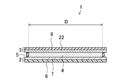
- the liquid crystal display device 1 includes a TFT substrate 2 that is a display device substrate on which a plurality of TFTs (Thin-FilmTransistors) that are switching elements are formed, and a TFT substrate 2 facing the TFT substrate 2. And a CF substrate 3 which is another display device substrate. Further, the liquid crystal display device 1 is sandwiched between a liquid crystal layer 4 which is a display medium layer sandwiched between the TFT substrate 2 and the CF substrate 3, and the TFT substrate 2 and the CF substrate 3. The substrate 2 and the CF substrate 3 are bonded to each other, and a sealing material 5 provided in a frame shape is provided to enclose the liquid crystal layer 4.
- TFT substrate 2 that is a display device substrate on which a plurality of TFTs (Thin-FilmTransistors) that are switching elements are formed
- a CF substrate 3 which is another display device substrate.
- the liquid crystal display device 1 is sandwiched between a liquid crystal layer 4
- the sealing material 5 is formed so as to circulate around the liquid crystal layer 4, and the TFT substrate 2 and the CF substrate 3 are bonded to each other via the sealing material 5.
- the TFT substrate 2 and the CF substrate 3 are each formed in a rectangular plate shape.
- the liquid crystal display device 1 includes a plurality of photo spacers (not shown) for regulating the thickness of the liquid crystal layer 4 (that is, the cell gap).
- a display area D for image display is defined in an area where the TFT substrate 2 and the CF substrate 3 overlap inside the sealing material 5. Yes.
- the display area D includes a plurality of pixels E (see FIGS. 3 and 8), which are the minimum unit of an image, arranged in a matrix.
- the liquid crystal display device 1 is formed in a rectangular shape, and in the longitudinal direction of the liquid crystal display device 1, the TFT substrate 2 protrudes from the CF substrate 3 on the upper side thereof.
- a terminal region T is defined in the protruding region.
- the terminal area T is provided around the display area D as shown in FIG.
- the terminal region T is provided with a plurality of terminals (not shown) and connection wiring (not shown) connected to each of the plurality of terminals.
- the TFT substrate 2 includes a substrate 6 having film-like flexibility (flexibility).
- a substrate 6 having film-like flexibility (flexibility) for example, a plastic substrate formed of an organic material such as polyimide resin, polyparaxylene resin, or acrylic resin can be used. Note that a metal substrate having flexibility may be used instead of the plastic substrate.
- a display element layer 7 provided with TFTs and the like is formed on the substrate 6 of the TFT substrate 2.
- the display element layer 7 includes a base coat layer 9 provided on the substrate 6, a plurality of gate wirings 11 extending in parallel to each other on the base coat layer 9, and And a gate insulating film 12 provided so as to cover each gate wiring 11.
- the display element layer 7 includes a plurality of source lines 14 extending in parallel with each other in a direction orthogonal to the gate lines 11 on the gate insulating film 12, and each intersection of the gate lines 11 and the source lines 14.
- a plurality of TFT elements 15 are provided, and a plurality of auxiliary capacitance lines 16 are provided between the gate lines 11 and extend in parallel to each other.
- the display element layer 7 is provided in a matrix on the interlayer insulating film 10 provided on the interlayer insulating film 10 so as to cover each gate wiring 11, each source wiring 14, and each TFT element 15.
- a plurality of pixel electrodes 19 connected to each of the elements 15 and an alignment film 20 provided so as to cover each pixel electrode 19 are provided.
- the TFT element 15 includes a gate electrode 27 in which each gate wiring 11 protrudes to the side, a gate insulating film 12 provided so as to cover the gate electrode 27, and the gate insulating film 12.
- the semiconductor layer 23 is provided in an island shape at a position overlapping the gate electrode 27, and the source electrode 28 and the drain electrode 29 are provided so as to face each other on the semiconductor layer 23.
- the source electrode 28 is a portion where each source wiring 14 protrudes to the side.
- the drain electrode 29 is connected to the pixel electrode 19 through a contact hole 30 formed in the interlayer insulating film 10 as shown in FIG.
- the pixel electrode 19 includes a transparent electrode 31 provided on the interlayer insulating film 10, and a reflective electrode 32 stacked on the transparent electrode 31 and provided on the surface of the transparent electrode 31. It is comprised by.
- the semiconductor layer 23 includes a lower intrinsic amorphous silicon layer 23 a and an upper n + amorphous silicon layer 23 b doped with phosphorus, and is exposed from the source electrode 28 and the drain electrode 29.
- the intrinsic amorphous silicon layer 23a that constitutes the channel region.
- drain electrode 29 forms an auxiliary capacitance by overlapping with the auxiliary capacitance wiring 16 through the gate insulating film 12.
- the material constituting the base coat layer 9 examples include materials such as silicon oxide (SiO 2 ), silicon nitride (SiNx (x is a positive number)), silicon oxynitride (SiNO), and the like. Note that the base coat layer 9 may have a laminated structure of these materials.
- the material constituting the gate insulating film 12 is not particularly limited.
- silicon oxide (SiO 2 ) a material having a lower dielectric constant than silicon oxide such as SiOF, SiOC, or the like, trisilicon tetranitride (Si 3 N 4 ) silicon nitride such as (SiNx (x is a positive number)), silicon oxynitride (SiNO), titanium dioxide (TiO 2), dialuminum trioxide (Al 2 O 3), tantalum pentoxide (Ta 2 O 5 ) And other materials having a higher dielectric constant than silicon oxide such as hafnium dioxide (HfO 2 ) and zirconium dioxide (ZrO 2 ).
- the gate insulating film 12 may have a single-layer structure or a stacked structure.
- the material constituting the interlayer insulating film 10 is not particularly limited, and examples thereof include insulating materials such as silicon oxide (SiO 2 ) and silicon nitride (SiNx (x is a positive number)).
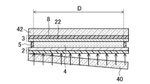
- the CF substrate 3 includes a substrate 8 having a film-like flexibility (flexibility) formed of a resin material, like the TFT substrate 2.
- a resin material like the TFT substrate 2.
- a plastic substrate formed of an organic material such as polyimide resin, polyparaxylene resin, or acrylic resin can be used.
- a metal substrate having flexibility may be used instead of the plastic substrate.
- a CF element layer 22 is formed on the substrate 8 of the CF substrate 3.
- the CF element layer 22 includes a color filter 48 provided on the substrate 8, a common electrode 24 provided so as to cover the reflective region of the color filter 48, and the common electrode 24.
- a photo spacer (not shown) provided in a column shape, and an alignment film 26 provided so as to cover the common electrode 24 and the photo spacer.
- the color filter 48 includes a plurality of types of colored layers 39 (that is, a red layer, a green layer, and a blue layer) provided for each pixel, and a black matrix that is a light shielding film. 36.
- the black matrix 36 is provided between adjacent colored layers 39 and has a role of partitioning these plural types of colored layers 39.
- the black matrix 36 is made of a metal material such as Ta (tantalum), Cr (chromium), Mo (molybdenum), Ni (nickel), Ti (titanium), Cu (copper), Al (aluminum), or a black pigment such as carbon.
- a metal material such as Ta (tantalum), Cr (chromium), Mo (molybdenum), Ni (nickel), Ti (titanium), Cu (copper), Al (aluminum), or a black pigment such as carbon.
- the photo spacer is made of, for example, an acrylic photosensitive resin, and is formed by a photolithography method.
- the thickness of the substrates 6 and 8 is preferably 3 to 30 ⁇ m. When the thickness is less than 3 ⁇ m, sufficient mechanical strength may not be obtained. When the thickness is greater than 30 ⁇ m, the substrate 6 is formed when the display element layer 7 and the CF element layer 22 are formed. , 8 becomes large and a problem may occur in the process.
- the liquid crystal layer 4 includes, for example, nematic liquid crystal having electro-optical characteristics.
- a reflection region R is defined by the reflection electrode 32 as shown in FIG. Further, the surface of the interlayer insulating film 10 under the pixel electrode 19 is formed in an uneven shape, and the surface of the reflective electrode 32 provided on the surface of the interlayer insulating film 10 via the transparent electrode 31 is also formed in an uneven shape. Has been.
- a liquid crystal display including a pixel electrode 19, a liquid crystal layer 4 formed on the pixel electrode 19, and a common electrode 24 formed on the liquid crystal layer 4 on the TFT substrate 2.
- An element 35 is provided.
- a polarizing plate (not shown) is provided outside the substrate 6 of the TFT substrate 2, and a backlight unit (not shown) is provided outside the polarizing plate.
- a polarizing plate (not shown) is provided outside the substrate 8 of the CF substrate 3.
- the reflective liquid crystal display device 1 having the above-described configuration is configured such that light incident from the CF substrate 3 side in the reflective region R is reflected by the reflective electrode 32.
- one pixel E is configured for each pixel electrode 19, and in each pixel E, when a gate signal is sent from the gate wiring 11 and the TFT element 15 is turned on, A source signal is sent from the source wiring 14 and a predetermined charge is written to the pixel electrode 19 through the source electrode 28 and the drain electrode 29, and a potential difference is generated between the pixel electrode 19 and the common electrode 24, and the liquid crystal layer 4 Is configured to be applied with a predetermined voltage.
- the reflectance of light incident from the CF substrate 3 side is adjusted using the fact that the alignment state of the liquid crystal molecules changes according to the magnitude of the applied voltage. Is displayed.
- a plurality of trench grooves 25 are provided in the vicinity of the TFT element 15 and the wiring (that is, the gate wiring 11 and the source wiring 14). There is a feature in that.
- the TFT substrate 2 is bent at the portion of the trench groove 25 that is resistant to stress as shown in FIG. Therefore, stress concentrates in the trench groove 25. Accordingly, a portion that is vulnerable to stress, for example, a crossing portion (wiring crossing portion) 33 of the gate wiring 11 and the source wiring 14 shown in FIG. 3 or a step portion in the TFT element 15 (that is, a step portion of the source electrode 28 or the drain electrode 29). ) It is possible to avoid the concentration of stress on 34, so that the disconnection of the wiring (that is, the gate wiring 11 and the source wiring 14) due to the bending and the damage to the TFT element 15 can be suppressed.
- a crossing portion (wiring crossing portion) 33 of the gate wiring 11 and the source wiring 14 shown in FIG. 3 or a step portion in the TFT element 15 that is, a step portion of the source electrode 28 or the drain electrode 29.
- the trench groove 25 is formed in the insulating film (that is, the gate insulating film 12 and the interlayer insulating film 10), and the pixel electrode 19 is provided on the surface of the trench groove 25. It has become.
- the trench groove 25 is formed along the gate line 11 and the source line 14. It is preferable to do.
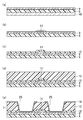
- FIG. 9 is a cross-sectional view for explaining a manufacturing method of the TFT substrate in the liquid crystal display device according to the first embodiment of the present invention, and more particularly, a diagram showing a manufacturing process of the TFT element.
- FIG. 10 is a cross-sectional view for explaining a method of manufacturing a TFT substrate in the liquid crystal display device according to the first embodiment of the present invention, and particularly shows a manufacturing process of a trench groove.
- FIG. 11 is a cross-sectional view for explaining the method for manufacturing the CF substrate in the liquid crystal display device according to the first embodiment of the present invention.
- FIGS. 12 to 14 are cross-sectional views for explaining the manufacturing method of the liquid crystal display device according to the first embodiment of the present invention.
- the manufacturing method shown below is a mere illustration, and the liquid crystal display device 1 which concerns on this invention is not limited to what was manufactured by the method shown below.
- ⁇ TFT substrate manufacturing process> Glass substrate preparation process
- a glass substrate 40 having a thickness of about 0.7 mm is prepared as a support substrate.
- a film-like flexible substrate 6 formed of, for example, a polyimide resin is formed on a glass substrate 40 with a thickness of, for example, about 20 ⁇ m. Form with.
- the substrate 6 may be formed by applying an organic material such as polyimide resin on the glass substrate 40.
- a base coat layer 9 made of, for example, silicon oxide (or silicon nitride) is formed on the substrate 6 by a method such as a CVD method.
- the molybdenum film having a single layer structure is exemplified as the metal film constituting the gate electrode 27.
- a metal such as an aluminum film, a tungsten film, a tantalum film, a chromium film, a titanium film, or a copper film is used.
- the gate electrode 27 may be formed with a thickness of 50 nm to 300 nm using a film, or an alloy film or a metal nitride film thereof.
- a silicon nitride film (thickness of about 200 nm to 500 nm) is formed by CVD on the entire substrate on which the gate wiring 11, the gate electrode 27, and the auxiliary capacitance wiring 16 are formed, and FIG. As shown in FIG. 10C, the gate insulating film 12 is formed so as to cover the gate wiring 11, the gate electrode 27, and the auxiliary capacitance wiring 16. Note that the gate insulating film 12 may have a two-layer structure.
- an intrinsic amorphous silicon film (thickness of about 2000 mm) and phosphorus-doped n + amorphous silicon film (thickness of about 500 mm) are formed on the entire substrate on which the gate insulating film 12 is formed by plasma CVD. Films are continuously formed. Thereafter, the semiconductor electrode is patterned on the gate electrode 27 by photolithography to form a semiconductor formation layer in which the intrinsic amorphous silicon layer 23a and the n + amorphous silicon layer 23b are stacked.
- an aluminum film and a titanium film are sequentially formed on the entire substrate on which the semiconductor formation layer has been formed by sputtering, and then patterned by photolithography to form the source wiring 14, the source electrode 28, and the drain.
- the electrode 29 is formed to a thickness of about 2000 mm.
- the n + amorphous silicon layer 23b of the semiconductor formation layer is etched by using the source electrode 28 and the drain electrode 29 as a mask to pattern the channel region, and as shown in FIG. A TFT element 15 having the same is formed.
- a silicon oxide film is formed by plasma CVD on the entire substrate on which the source electrode 28 and the drain electrode 29 are formed (that is, the TFT element 15 is formed), and FIG.
- the interlayer insulating film 10 covering the TFT element 15 is formed to a thickness of about 265 nm, for example. To do.
- a photomask having a predetermined pattern is formed on the interlayer insulating film 10 by photolithography.
- exposure and development are performed using this photomask, and patterning is performed using an etching method, whereby the interlayer insulating film 10 is etched as shown in FIG. 30 is formed, and as shown in FIG. 10E, the interlayer insulating film 10 and the gate insulating film 12 are etched to form a trench groove 25.
- the trench groove 25 in the formation of the contact hole, can be formed simultaneously with the contact hole 30 only by changing the design of the photomask that has been conventionally used.
- the trench groove 25 can be formed without any problem.
- the gate insulating film 12 and the interlayer insulating film 10 are formed of a photosensitive resin (for example, acrylic photosensitive resin), and a halftone mask or a gray tone mask is used as a photomask to perform exposure processing (halftone).
- the trench groove 25 may be formed by controlling the exposure amount irradiated to the photosensitive resin by performing an exposure process or a gray tone exposure process. Further, the trench groove 25 can be formed by pressing a convex mold or the like against the gate insulating film 12 and the interlayer insulating film 10.
- a transparent conductive film such as an ITO film (thickness of about 50 nm to 200 nm) made of indium tin oxide is formed on the entire substrate on which the interlayer insulating film 10 is formed by sputtering, and then the transparent conductive film By performing photolithography, wet etching, and resist peeling and cleaning on the film, the pixel electrode 19 is formed as shown in FIGS. 9F and 10E.
- the pixel electrode 19 has the surfaces of the interlayer insulating film 10 and the gate insulating film 12 so as to cover the surfaces of the trench groove 25 and the contact hole 30. Formed on top.
- a polyimide resin is applied to the entire substrate by a printing method, and then a rubbing process is performed to form the alignment film 20.
- a photo spacer made of an acrylic photosensitive resin is formed on the entire substrate by using, for example, a photolithography method.
- the TFT substrate 2 in which the display element layer 7 including the TFT elements 15 and the trench grooves 25 is formed on the substrate 6 can be manufactured.
- a glass substrate 42 having a thickness of about 0.7 mm is prepared as a support substrate.
- a film-like flexible substrate 8 made of, for example, a polyimide resin is formed on the glass substrate 42 with a thickness of about 20 ⁇ m, for example.
- the color filter 48 including the colored layer 39 and the black matrix 36 is formed on the substrate 8, and the common electrode 24 and the like are patterned to form the CF element layer 22. Thereafter, a polyimide resin is applied to the entire substrate by a printing method, and then a rubbing process is performed to form an alignment film 26, whereby the CF substrate 3 constituting the display region D is manufactured.
- ⁇ TFT substrate / CF substrate bonding process First, for example, using a dispenser, the sealing material 5 made of ultraviolet curing and thermosetting resin or the like is drawn on the CF substrate 3 in a frame shape.
- a liquid crystal material for forming the liquid crystal layer 4 is dropped on a region inside the sealing material 5 in the CF substrate 3 on which the sealing material 5 is drawn.
- the CF substrate 3 onto which the liquid crystal material is dropped and the TFT substrate 2 are bonded together under reduced pressure.
- the front and back surfaces of the bonded body are pressurized by releasing the bonded body to atmospheric pressure. Then, after irradiating the sealing material 5 sandwiched between the bonded bodies with UV light, the sealing material 5 is cured by heating the bonded body, and as shown in FIG. 12, the TFT substrate 2 and the CF substrate 3 A bonded body in which is bonded is produced.
- the glass substrate 40 is peeled off by irradiating laser light (arrows in FIG. 13) from the glass substrate 40 side.
- the removal of the glass substrate 40 may not be peeling by laser light irradiation.
- the glass substrate 40 may be removed using a polishing or etching apparatus.
- the glass substrate 42 is peeled off by irradiating laser light (arrows in FIG. 14) from the glass substrate 42 side.
- the removal of the glass substrate 42 may not be peeling by laser light irradiation, as in the case of the glass substrate 40 described above.
- the glass substrate 42 may be removed using a polishing or etching apparatus.
- a polarizing plate (not shown) and a backlight unit (not shown) are provided to complete the liquid crystal display device 1 shown in FIG.
- the trench groove 25 is provided in the vicinity of the TFT element 15 and the wiring (gate wiring 11 and source wiring 14). Accordingly, even when an external force is applied to the TFT substrate 2, the TFT substrate 2 bends at the portion of the trench groove 25 that is resistant to stress, so that the stress is concentrated in the trench groove 25. Accordingly, concentration of stress on the wiring (gate wiring 11 and source wiring 14) and the TFT element 15 that are vulnerable to stress can be avoided, and therefore, disconnection of wiring due to bending and damage to the TFT element 15 can be suppressed. Can do. As a result, the yield of the TFT substrate 2 can be improved.
- a plurality of trench grooves 25 are provided. Therefore, since it is possible to further avoid stress concentration on the wiring and the TFT element 15 which are vulnerable to stress, it is possible to further suppress the disconnection of the wiring and the damage to the TFT element 15 caused by bending.
- the trench groove 25 is formed along the gate wiring 11 and the source wiring 14. Therefore, in particular, stress concentration on the gate wiring 11 and the source wiring 14 can be further avoided, so that disconnection of the gate wiring 11 and the source wiring 14 due to bending can be further suppressed.
- the trench groove 25 is provided at the periphery of each of the plurality of pixels E. Therefore, the trench groove 25 can be provided without considering the influence on the image display.
- the trench groove 25 is formed in the insulating film (that is, the gate insulating film 12 and the interlayer insulating film 10). Therefore, it is possible to provide a device resistant to stress by simple trench formation.
- FIG. 15 is a cross-sectional view showing a trench formed in the TFT substrate according to the second embodiment of the present invention. Note that the same components as those in the first embodiment are denoted by the same reference numerals, and description thereof is omitted. Further, the overall configuration of the liquid crystal display device is the same as that described in the first embodiment, and therefore detailed description thereof is omitted here.
- the trench groove 25 is formed in the gate insulating film 12 and the interlayer insulating film 10 as shown in FIG. 7, but in this embodiment, as shown in FIG. A feature is that a trench groove 38 is formed in the gate insulating film 12 and the interlayer insulating film 10.
- the trench groove 38 has a depth greater than that of the trench groove 25 described above. Therefore, when an external force such as mechanical stress acts on the TFT substrate 2, the trench groove resistant to stress.
- the liquid crystal display device 1 is easily bent at the portion 38, and stress is further concentrated in the trench groove 38. Therefore, it is possible to further avoid stress concentration on the intersection 33 of the gate wiring 11 and the source wiring 14 and the step portion 34 of the source electrode 28 and the drain electrode in the TFT element 15, which is weak against stress. The disconnection of the wiring to be performed and the damage to the TFT element 15 can be further suppressed.
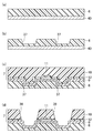
- FIG. 16 is a diagram showing a manufacturing process of a trench groove according to the second embodiment of the present invention.
- the TFT element manufacturing process, the CF substrate manufacturing process, and the TFT substrate / CF substrate bonding process are the same as those described in the first embodiment, and a detailed description thereof is omitted here.
- the glass substrate 40 about 0.7 mm thick is prepared as a support substrate, for example.
- a film-like flexible substrate 6 formed of, for example, a polyimide resin is formed on the glass substrate 40 with a thickness of about 20 ⁇ m, for example.
- a photoresist is formed on the substrate 6 by photolithography, and the photoresist is ashed to remove a portion corresponding to the trench groove of the photoresist. Then, using this photoresist as a photomask, patterning is performed using an etching method, thereby forming a groove 37 to be a part of the trench groove 38 in the substrate 6 as shown in FIG. .
- the base coat layer 9, the gate wiring 11, the gate insulating film 12, and the interlayer insulating film 10 are formed.
- the base coat layer 9 is formed on the surface of the substrate 6 so as to cover the surface of the groove 37.
- a photomask having a predetermined pattern is formed by photolithography, exposure and development are performed using this photomask, and patterning is performed using an etching method.
- the interlayer insulating film 10 and the gate insulating film 12 are etched to form a trench groove 38.
- the interlayer insulating film 10 is etched to form the contact hole 30.
- the pixel electrode 19 is formed, and the alignment film 20 and the spacer are formed, whereby the TFT substrate 2 in which the display element layer 7 is formed on the substrate 6 is manufactured. can do.
- the trench groove 38 is formed in the substrate 6 and the insulating film (that is, the gate insulating film 12 and the interlayer insulating film 10). Accordingly, it is possible to form the trench groove 38 that is resistant to stress with a simple configuration. Further, since the trench groove 38 having a large depth can be formed, the TFT substrate 2 is easily bent at the trench groove 38, and stress can be further concentrated in the trench groove 38. Therefore, stress concentration on the wiring and the TFT element 15 that is vulnerable to stress can be further avoided, and thus disconnection of the wiring due to bending and damage to the TFT element 15 can be further suppressed.
- the trench groove 25 is formed in the gate insulating film 12 and the interlayer insulating film 10.
- a trench groove may be formed only in the upper interlayer insulating film 10.
- trench grooves 25 and 38 described above may be provided close to the auxiliary capacitance wiring 16.
- an LCD liquid crystal display
- the display device is not limited to this, and a TFT element is formed on a flexible substrate. Any display device may be used as long as it includes a display device substrate having a display element layer on which wiring is formed.
- organic EL organic electroluminescence
- electrophoresis electrophoretic
- PD plasma display
- PALC plasma addressed liquid crystal display
- inorganic EL inorganic electroluminescence
- FED field It may be a display device related to emission S display (field emission display) or SED (surface-conduction electron-emitter display).
- the semiconductor layer 23 has been described by taking an example of amorphous silicon.
- a semiconductor layer made of polysilicon or continuous grain boundary crystal (CG) silicon may be used.
- CG continuous grain boundary crystal
- IGZO indium gallium zinc oxide
- the present invention is particularly useful for a display device substrate including a plastic substrate and a display device including the same.
- Liquid crystal display device 2 TFT substrate (display device substrate) 3 CF substrate 4 Liquid crystal layer 6 Substrate 7 Display element layer 8 Substrate 10 Interlayer insulating film (insulating film) 11 Gate wiring (wiring) 12 Gate insulating film (insulating film) 14 Source wiring (wiring) 15 TFT element (switching element) 16 Auxiliary Capacitor Line 19 Pixel Electrode 22 CF Element Layer 23 Semiconductor Layer 24 Common Electrode 25 Trench Groove 27 Gate Electrode 28 Source Electrode 29 Drain Electrode 30 Contact Hole 33 Intersection of Gate Line and Source Line 34 Stepped Part 35 in TFT Element 35 Liquid Crystal Display Element (display element) 38 trench groove 40 glass substrate 42 glass substrate 48 color filter
Landscapes
- Liquid Crystal (AREA)
- Devices For Indicating Variable Information By Combining Individual Elements (AREA)
Abstract
TFT基板(3)は、可撓性を有する基板と、基板上に形成され、TFT素子(15)、ゲート配線(11)、及びソース配線(14)を有する表示素子層と、TFT素子(15)、ゲート配線(11)、及びソース配線(14)に近接して設けられたトレンチ溝(25)とを備える。
Description
本発明は、プラスチック基板を備えた表示装置用基板及びそれを備えた表示装置に関する。
近年、ディスプレイ分野では、フレキシブル性、耐衝撃性や軽量性の点でガラス基板に比べて大きなメリットのあるプラスチック基板等の可撓性を有する基板を用いた表示装置が非常に注目を浴びており、ガラス基板のディスプレイでは不可能であった新たな表示装置が創出される可能性を秘めている。
このような表示装置としては、例えば、互いに対向して配置された一対の表示装置用基板(即ち、TFT(Thin Film Transistor)基板とCF(Color Filter)基板)と、一対の基板の間に設けられた液晶層とを有する液晶表示装置が提案されている。
この液晶表示装置では、TFT基板は、可撓性を有するプラスチック基板と、プラスチック基板上に設けられ、スイッチング素子であるTFT素子を有する表示素子層とを備えている。また、CF基板は、上述のプラスチック基板と、プラスチック基板上に設けられたCF素子層とを備えている(例えば、特許文献1参照)。
また、一般に、このTFT基板には、プラスチック基板上に互いに平行に延びるように設けられた複数のゲート配線や、各ゲート配線と直交する方向に互いに平行に延びるように設けられた複数のソース配線等の配線が設けられている。そして、各ゲート配線及び各ソース配線の交差部分毎、すなわち、各画素毎に上述のTFT素子が設けられる構成となっている。
ここで、フレキシブル性を有する表示装置においては、機械的なストレス等の外力により表示装置が屈曲し易いため、当該屈曲に起因して、表示装置の所定箇所に応力が集中してしまい、上記配線の断線や、TFT素子の破損が発生するという問題があった。また、特に、製造工程において、このような配線の断線やTFT素子の破損が発生すると、表示装置用基板の歩留まりが低下するという問題が生じていた。
そこで、本発明は、上述の問題に鑑みてなされたものであり、フレキシブル性を有するとともに良好な表示性能を有し、屈曲に起因する配線の断線やTFT素子の破損の発生を抑制して、歩留まりを向上することができる表示装置用基板およびそれを備えた表示装置を提供することを目的とする。
上記目的を達成するために、本発明の表示装置用基板は、可撓性を有する基板と、基板上に形成され、スイッチング素子と配線とを有する表示素子層と、スイッチング素子及び配線に近接して設けられたトレンチ溝とを備えることを特徴とする。
同構成によれば、機械的なストレス等の外力が表示装置用基板に作用した場合であっても、ストレスに強いトレンチ溝の部分で表示装置用基板が屈曲することになるため、トレンチ溝に応力が集中することになる。従って、ストレスに弱い配線やスイッチング素子への応力の集中を回避することができるため、屈曲に起因する配線の断線や、スイッチング素子の破損を抑制するこができる。特に、製造工程の途中で生じやすい配線の断線や、スイッチング素子の破損を抑制するこができる。また、スイッチング素子において、破損に起因する閾値電圧の変動を抑制することができるため、スイッチング素子の特性の低下を抑制することができる。その結果、表示装置用基板の歩留まりを向上することができる。
また、本発明の表示装置用基板においては、トレンチ溝を複数設ける構成としてもよい。
同構成によれば、ストレスに弱い配線やスイッチング素子への応力の集中を一層回避することができるため、屈曲に起因する配線の断線や、スイッチング素子の破損を一層抑制するこができる。
また、本発明の表示装置用基板においては、トレンチ溝を、配線に沿って形成する構成としてもよい。同構成によれば、特に、配線への応力の集中を一層回避することができるため、屈曲に起因する配線の断線を一層抑制するこができる。
また、本発明の表示装置用基板においては、マトリクス状に配列された複数の画素を更に備え、トレンチ溝が、複数の画素の各々の周縁に設けられる構成としてもよい。
同構成によれば、画像表示への影響を考慮することなく、トレンチ溝を設けることが可能になる。
また、本発明の表示装置用基板においては、表示素子層は、スイッチング素子及び配線を覆う絶縁膜を有し、トレンチ溝を、絶縁膜に形成する構成としてもよい。
同構成によれば、簡単なトレンチ形成により、ストレスに強いデバイスを提供することが可能になる。
また、本発明の表示装置用基板においては、表示素子層は、スイッチング素子及び配線を覆う絶縁膜を有し、トレンチ溝を、基板と絶縁膜に形成する構成としてもよい。
同構成によれば、簡単な構成で、ストレスに強いトレンチ溝を形成することが可能になる。また、深さの大きなトレンチ溝を形成することができるため、トレンチ溝の部分で表示装置用基板が屈曲し易くなり、トレンチ溝に、より一層応力を集中させることができる。従って、ストレスに弱い配線やスイッチング素子への応力の集中を、より一層回避することができるため、屈曲に起因する配線の断線や、スイッチング素子の破損をより一層抑制するこができる。
また、本発明の表示装置用基板においては、配線が、基板上に互いに平行に延設された複数のゲート配線と、複数のゲート配線の各々と直交する方向に互いに平行に延設された複数のソース配線であり、スイッチング素子が、ゲート配線及びソース配線の交差部分毎に設けられている構成としてもよい。
同構成によれば、特に、ストレスに弱い、ゲート配線とソース配線の交差部分やスイッチング素子における段差部分への応力の集中を回避することができる。
また、本発明の表示装置用基板においては、スイッチング素子が、TFT素子であつてもよい。
また、本発明の表示装置用基板は、屈曲に起因する配線の断線や、スイッチング素子の破損を抑制して、表示装置用基板の歩留まりを向上することができるという優れた特性を備えている。従って、本発明の表示装置用基板は、表示装置用基板と表示装置用基板上に形成された表示素子とを備える表示装置に好適に使用できる。また、本発明の表示装置は、表示素子が液晶表示素子である表示装置に好適に使用できる。
本発明によれば、可撓性を有する基板を備える表示装置用基板において、屈曲に起因する配線の断線やスイッチング素子の破損を抑制して、表示装置用基板の歩留まりを向上することができる。
(第1の実施形態)
以下、本発明の実施形態を図面に基づいて詳細に説明する。
以下、本発明の実施形態を図面に基づいて詳細に説明する。
図1は、本発明の第1の実施形態に係る液晶表示装置の全体構成を示す平面図であり、図2は、図1のA-A断面図である。また、図3は、本発明の第1の実施形態に係るTFT基板の画素部を拡大した平面図であり、図4は、本発明の第1の実施形態に係る液晶表示装置を構成するTFT基板の全体構成を示す断面図である。また、図5は、本発明の第1の実施形態に係る液晶表示装置の表示部の全体構成を示す断面図であり、図6は、本発明の第1の実施形態に係るTFT基板を屈曲した状態を示す斜視図である。また、図7は、図3のB-B断面図である。なお、本実施形態においては、表示装置として、液晶表示装置を例に挙げて説明する。
図1、図2に示すように、液晶表示装置1は、スイッチング素子であるTFT(Thin-Film Transistor)が複数形成された表示装置用基板であるTFT基板2と、TFT基板2に対向して配置された他の表示装置用基板であるCF基板3とを備えている。また、液晶表示装置1は、TFT基板2及びCF基板3の間に挟持して設けられた表示媒体層である液晶層4と、TFT基板2とCF基板3との間に狭持され、TFT基板2及びCF基板3を互いに接着するとともに液晶層4を封入するために枠状に設けられたシール材5とを備えている。
このシール材5は、液晶層4を周回するように形成されており、TFT基板2とCF基板3は、このシール材5を介して相互に貼り合わされている。なお、TFT基板2及びCF基板3は、それぞれ矩形板状に形成されている。また、液晶表示装置1は、液晶層4の厚み(即ち、セルギャップ)を規制するための複数のフォトスペーサ(不図示)を備えている。
また、液晶表示装置1では、図1、図2に示すように、シール材5の内側であって、TFT基板2及びCF基板3が重なる領域に、画像表示を行う表示領域Dが規定されている。ここで、表示領域Dは、画像の最小単位である画素E(図3、図8参照)がマトリクス状に複数配列して構成されている。
また、図1に示すように、液晶表示装置1は、矩形状に形成されており、液晶表示装置1の長手方向において、TFT基板2がその上辺においてCF基板3よりも突出している。そして、その突出した領域には、端子領域Tが規定されている。この端子領域Tは、図1に示すように、表示領域Dの周辺に設けられている。
また、端子領域Tには、図1に示すように、複数の端子(不図示)と、当該複数の端子の各々に接続された接続用の配線(不図示)とが設けられている。
TFT基板2は、フィルム状の可撓性(フレキシビリティー)を有する基板6を備える。この基板6としては、例えば、ポリイミド樹脂、ポリパラキシレン樹脂、アクリル樹脂等の有機材料により形成されたプラスチック基板を用いることができる。なお、プラスチック基板の代わりに、可撓性を有する金属基板を使用する構成としても良い。
また、TFT基板2の基板6上には、TFT等を備えた表示素子層7が形成されている。
ここで、表示素子層7は、図3,図4に示すように、基板6上に設けられたベースコート層9と、ベースコート層9上に互いに平行に延設された複数のゲート配線11と、各ゲート配線11を覆うように設けられたゲート絶縁膜12とを備えている。また、表示素子層7は、ゲート絶縁膜12上に各ゲート配線11と直交する方向に互いに平行に延設された複数のソース配線14と、各ゲート配線11及び各ソース配線14の交差部分毎にそれぞれ設けられた複数のTFT素子15と、各ゲート配線11の間にそれぞれ設けられ、互いに平行に延設された複数の補助容量配線16とを備えている。更に、表示素子層7は、各ゲート配線11、各ソース配線14、及び各TFT素子15を覆うように設けられた層間絶縁膜10と、層間絶縁膜10上にマトリクス状に設けられ、各TFT素子15の各々に接続された複数の画素電極19と、各画素電極19を覆うように設けられた配向膜20とを有している。
また、TFT素子15は、図4に示すように、各ゲート配線11が側方に突出したゲート電極27と、ゲート電極27を覆うように設けられたゲート絶縁膜12と、ゲート絶縁膜12上でゲート電極27に重なる位置において島状に設けられた半導体層23と、半導体層23上で互いに対峙するように設けられたソース電極28及びドレイン電極29とを備えている。
ここで、ソース電極28は、各ソース配線14が側方に突出した部分である。また、ドレイン電極29は、図4に示すように、層間絶縁膜10に形成されたコンタクトホール30を介して画素電極19に接続されている。
また、画素電極19は、図5に示すように、層間絶縁膜10上に設けられた透明電極31と、透明電極31上に積層され、透明電極31の表面上に設けられた反射電極32とにより構成されている。
また、半導体層23は、図4に示すように、下層の真性アモルファスシリコン層23aと、その上層のリンがドープされたn+アモルファスシリコン層23bとを備え、ソース電極28及びドレイン電極29から露出する真性アモルファスシリコン層23aがチャネル領域を構成している。
また、ドレイン電極29は、ゲート絶縁膜12を介して、補助容量配線16と重なることにより補助容量を構成している。
ベースコート層9を構成する材料としては、例えば、酸化シリコン(SiO2)、窒化シリコン(SiNx(xは正数))、シリコンオキシナイトライド(SiNO)等の材料が挙げられる。なお、ベースコート層9は、これらの材料による積層構造としても良い。
ゲート絶縁膜12を構成する材料としては、特に限定されず、例えば、酸化シリコン(SiO2)や、SiOF、SiOC等の酸化シリコンよりも誘電率が低い材料、四窒化三ケイ素(Si3N4)等の窒化シリコン(SiNx(xは正数))、シリコンオキシナイトライド(SiNO)、二酸化チタン(TiO2)、三酸化二アルミニウム(Al2O3)、五酸化二タンタル(Ta2O5)等の酸化タンタル、二酸化ハフニウム(HfO2)、二酸化ジルコニウム(ZrO2)等の酸化シリコンよりも誘電率が高い材料が挙げられる。なお、ゲート絶縁膜12は、単層構造であってもよいし、積層構造であってもよい。
層間絶縁膜10を構成する材料としては、特に限定されず、例えば、酸化シリコン(SiO2)、窒化シリコン(SiNx(xは正数))等の絶縁性材料が挙げられる。
また、CF基板3は、TFT基板2と同様に、樹脂材料により形成されたフィルム状の可撓性(フレキシビリティー)を有する基板8を備える。この基板8としては、例えば、ポリイミド樹脂、ポリパラキシレン樹脂、アクリル樹脂等の有機材料により形成されたプラスチック基板を用いることができる。なお、プラスチック基板の代わりに、可撓性を有する金属基板を使用する構成としても良い。
また、CF基板3の基板8上には、CF素子層22が形成されている。ここで、CF素子層22は、図5に示すように、基板8上に設けられたカラーフィルター48と、カラーフィルター48の反射領域を覆うように設けられた共通電極24と、共通電極24上に柱状に設けられたフォトスペーサ(不図示)と、共通電極24及びフォトスペーサを覆うように設けられた配向膜26とを有している。
なお、カラーフィルター48には、図5に示すように、各画素に対して設けられた複数種の着色層39(即ち、赤色層、緑色層、および青色層)と、遮光膜であるブラックマトリクス36とが含まれる。ブラックマトリクス36は、隣接する着色層39の間に設けられ、これら複数種の着色層39を区画する役割を有するものである。
このブラックマトリクス36は、Ta(タンタル)、Cr(クロム)、Mo(モリブデン)、Ni(ニッケル)、Ti(チタン)、Cu(銅)、Al(アルミニウム)などの金属材料、カーボンなどの黒色顔料が分散された樹脂材料、または、各々、光透過性を有する複数色の着色層が積層された樹脂材料などにより形成される。また、フォトスペーサは、例えば、アクリル系の感光性樹脂からなり、フォトリソグラフィー法により形成される。
なお、基板6,8の厚みとしては、3~30μmが好ましい。これは、厚みが3μm未満の場合は、十分な機械的強度が得られない場合があり、また、30μmよりも大きい場合は、表示素子層7やCF素子層22を形成する際に、基板6,8の反りが大きくなり、プロセス上、問題が生じる場合があるからである。
液晶層4は、例えば、電気光学特性を有するネマチック液晶を含んでいる。
また、液晶表示装置1の表示部では、図5に示すように、反射電極32により反射領域Rが規定されている。また、画素電極19の下層の層間絶縁膜10の表面は、凹凸状に形成されており、層間絶縁膜10の表面に透明電極31を介して設けられた反射電極32の表面も凹凸状に形成されている。
そして、本実施形態においては、TFT基板2上に、画素電極19と、画素電極19上に形成された液晶層4と、液晶層4上に形成された共通電極24とにより構成された液晶表示素子35が設けられている。
なお、TFT基板2の基板6の外側には、偏光板(不図示)が設けられるとともに、当該偏光板の外側にはバックライトユニット(不図示)が設けられている。また、CF基板3の基板8の外側には、偏光板(不図示)が設けられている。
そして、上記構成の反射型の液晶表示装置1は、反射領域RにおいてCF基板3側から入射する光を反射電極32で反射するように構成されている。
そして、液晶表示装置1は、各画素電極19毎に1つの画素Eが構成されており、各画素Eにおいて、ゲート配線11からゲート信号が送られてTFT素子15をオン状態にした場合に、ソース配線14からソース信号が送られてソース電極28及びドレイン電極29を介して、画素電極19に所定の電荷が書き込まれ、画素電極19と共通電極24との間で電位差が生じ、液晶層4に所定の電圧が印加されるように構成されている。
そして、液晶表示装置1では、印加された電圧の大きさに応じて、液晶分子の配向状態が変わることを利用して、CF基板3側から入射する光の反射率を調整することにより、画像が表示される構成となっている。
ここで、本実施形態のTFT基板2においては、図3に示すように、TFT素子15及び配線(即ち、ゲート配線11とソース配線14)に近接して、複数のトレンチ溝25が設けられている点に特徴がある。
このような構成により、機械的なストレス等の外力がTFT基板2に作用した場合であっても、図6に示すように、ストレスに強いトレンチ溝25の部分でTFT基板2が屈曲することになるため、トレンチ溝25に応力が集中することになる。従って、ストレスに弱い箇所、例えば、図3に示す、ゲート配線11とソース配線14の交差部分(配線乗り越え部分)33やTFT素子15における段差部分(即ち、ソース電極28やドレイン電極29の段差部分)34への応力の集中を回避することができるため、屈曲に起因する配線(即ち、ゲート配線11やソース配線14)の断線や、TFT素子15の破損を抑制するこができる。特に、製造工程の途中で生じやすい配線(即ち、ゲート配線11やソース配線14)の断線や、TFT素子15の破損を抑制するこができる。また、TFT素子15においては、破損に起因する閾値電圧の変動を抑制することができるため、TFT特性の低下を抑制することができる。その結果、TFT基板2の歩留まりを向上することができる。
また、トレンチ溝25は、図7に示すように、絶縁膜(即ち、ゲート絶縁膜12及び層間絶縁膜10)に形成されており、当該トレンチ溝25の表面に画素電極19が設けられる構成となっている。
また、画像表示への影響を最小限にするとの観点から、図8に示すように、トレンチ溝25は、各画素Eにおいて、当該画素Eの周縁に設けることが好ましい。
また、特に、ゲート配線11とソース配線14への応力の集中を一層回避するとの観点から、図3、図8に示すように、トレンチ溝25を、ゲート配線11とソース配線14に沿って形成することが好ましい。
次に、本発明の実施形態に係る液晶表示装置1の製造方法について説明する。図9は、本発明の第1の実施形態に係る液晶表示装置におけるTFT基板の製造方法を説明するための断面図であり、特に、TFT素子の製造工程を示す図である。また、図10は、本発明の第1の実施形態に係る液晶表示装置におけるTFT基板の製造方法を説明するための断面図であり、特に、トレンチ溝の製造工程を示す図である。また、図11は、本発明の第1の実施形態に係る液晶表示装置におけるCF基板の製造方法を説明するための断面図である。また、図12~図14は、本発明の第1の実施形態に係る液晶表示装置の製造方法を説明するための断面図である。なお、以下に示す製造方法は単なる例示であり、本発明に係る液晶表示装置1は以下に示す方法により製造されたものに限定されるものではない。
<TFT基板作製工程>
(ガラス基板準備工程)
まず、図9(a)、図10(a)に示すように、支持基板として、例えば、厚さ0.7mm程度のガラス基板40を準備する。
(ガラス基板準備工程)
まず、図9(a)、図10(a)に示すように、支持基板として、例えば、厚さ0.7mm程度のガラス基板40を準備する。
(プラスチック基板形成工程)
次いで、図9(a)、図10(a)に示すように、ガラス基板40上に、例えば、ポリイミド樹脂により形成されたフィルム状の可撓性を有する基板6を、例えば、20μm程度の厚みで形成する。
次いで、図9(a)、図10(a)に示すように、ガラス基板40上に、例えば、ポリイミド樹脂により形成されたフィルム状の可撓性を有する基板6を、例えば、20μm程度の厚みで形成する。
なお、ガラス基板40上に、ポリイミド樹脂等の有機材料を塗布することにより、基板6を形成してもよい。
(ベースコート層形成工程)
次いで、図9(a)、図10(a)に示すように、基板6上に、CVD法等の方法により、例えば、酸化シリコン(または、窒化シリコン)からなるベースコート層9を形成する。
次いで、図9(a)、図10(a)に示すように、基板6上に、CVD法等の方法により、例えば、酸化シリコン(または、窒化シリコン)からなるベースコート層9を形成する。
(ゲート電極形成工程)
次いで、ベースコート層9上に、スパッタリング法により、例えば、モリブテン膜(厚さ150nm程度)などを成膜した後に、そのモリブテン膜に対して、フォトリソグラフィ、ウエットエッチング及びレジストの剥離洗浄を行うことにより、図3、図9(b)、図10(b)に示すように、ゲート配線11、ゲート電極27、及び補助容量配線16を形成する。
次いで、ベースコート層9上に、スパッタリング法により、例えば、モリブテン膜(厚さ150nm程度)などを成膜した後に、そのモリブテン膜に対して、フォトリソグラフィ、ウエットエッチング及びレジストの剥離洗浄を行うことにより、図3、図9(b)、図10(b)に示すように、ゲート配線11、ゲート電極27、及び補助容量配線16を形成する。
なお、本実施形態では、ゲート電極27を構成する金属膜として、単層構造のモリブテン膜を例示したが、例えば、アルミニウム膜、タングステン膜、タンタル膜、クロム膜、チタン膜、銅膜等の金属膜、または、これらの合金膜や金属窒化物による膜によりゲート電極27を、50nm~300nmの厚さで形成する構成としても良い。
(ゲート絶縁膜形成工程)
次いで、ゲート配線11、ゲート電極27、補助容量配線16が形成された基板全体に、CVD法により、例えば、窒化シリコン膜(厚さ200nm~500nm程度)を成膜して、図9(c)、図10(c)に示すように、ゲート配線11、ゲート電極27、及び補助容量配線16を覆うようにゲート絶縁膜12を形成する。なお、ゲート絶縁膜12を2層の積層構造で形成する構成としても良い。
次いで、ゲート配線11、ゲート電極27、補助容量配線16が形成された基板全体に、CVD法により、例えば、窒化シリコン膜(厚さ200nm~500nm程度)を成膜して、図9(c)、図10(c)に示すように、ゲート配線11、ゲート電極27、及び補助容量配線16を覆うようにゲート絶縁膜12を形成する。なお、ゲート絶縁膜12を2層の積層構造で形成する構成としても良い。
(半導体層・ソースドレイン形成工程)
次いで、ゲート絶縁膜12が形成された基板全体に、プラズマCVD法により、例えば、真性アモルファスシリコン膜(厚さ2000Å程度)、及びリンがドープされたn+アモルファスシリコン膜(厚さ500Å程度)を連続して成膜する。その後、フォトリソグラフィによりゲート電極27上に島状にパターニングして、真性アモルファスシリコン層23a及びn+アモルファスシリコン層23bが積層された半導体形成層を形成する。
次いで、ゲート絶縁膜12が形成された基板全体に、プラズマCVD法により、例えば、真性アモルファスシリコン膜(厚さ2000Å程度)、及びリンがドープされたn+アモルファスシリコン膜(厚さ500Å程度)を連続して成膜する。その後、フォトリソグラフィによりゲート電極27上に島状にパターニングして、真性アモルファスシリコン層23a及びn+アモルファスシリコン層23bが積層された半導体形成層を形成する。
そして、上記半導体形成層が形成された基板全体に、スパッタリング法により、例えば、アルミニウム膜及びチタン膜などを順に成膜し、その後、フォトリソグラフィによりパターニングして、ソース配線14、ソース電極28及びドレイン電極29を厚さ2000Å程度に形成する。
次いで、ソース電極28及びドレイン電極29をマスクとして上記半導体形成層のn+アモルファスシリコン層23bをエッチングすることにより、チャネル領域をパターニングして、図9(d)に示すように、半導体層23及びそれを備えたTFT素子15を形成する。
(層間絶縁膜形成工程)
次いで、ソース電極28及びドレイン電極29が形成された(即ち、TFT素子15が形成された)基板の全体に、プラズマCVD法により、例えば、酸化シリコン膜を成膜し、図9(e)、図10(d)に示すように、TFT素子15を覆う(即ち、半導体層23、ゲート電極27、ソース電極28及びドレイン電極29を覆う)層間絶縁膜10を、例えば、厚さ265nm程度に形成する。
次いで、ソース電極28及びドレイン電極29が形成された(即ち、TFT素子15が形成された)基板の全体に、プラズマCVD法により、例えば、酸化シリコン膜を成膜し、図9(e)、図10(d)に示すように、TFT素子15を覆う(即ち、半導体層23、ゲート電極27、ソース電極28及びドレイン電極29を覆う)層間絶縁膜10を、例えば、厚さ265nm程度に形成する。
(トレンチ溝・コンタクトホール形成工程)
次いで、層間絶縁膜10上に、フォトリソグラフィにより所定のパターンを有するフォトマスクを形成する。次いで、このフォトマスクを使用して、露光、現像を行い、エッチング法を使用してパターンニングを行うことにより、図9(f)に示すように、層間絶縁膜10をエッチングして、コンタクトホール30を形成するとともに、図10(e)に示すように、層間絶縁膜10とゲート絶縁膜12とをエッチングして、トレンチ溝25を形成する。
次いで、層間絶縁膜10上に、フォトリソグラフィにより所定のパターンを有するフォトマスクを形成する。次いで、このフォトマスクを使用して、露光、現像を行い、エッチング法を使用してパターンニングを行うことにより、図9(f)に示すように、層間絶縁膜10をエッチングして、コンタクトホール30を形成するとともに、図10(e)に示すように、層間絶縁膜10とゲート絶縁膜12とをエッチングして、トレンチ溝25を形成する。
このように、本実施形態においては、コンタクトホール形成において、従来、使用していたフォトマスクの設計変更のみで、コンタクトホール30と同時にトレンチ溝25を形成することができるため、製造工程を増加することなく、トレンチ溝25を形成することができる。
なお、ゲート絶縁膜12及び層間絶縁膜10を感光性樹脂(例えば、アクリル系の感光性樹脂)で形成するとともに、フォトマスクとして、ハーフトーンマスク又はグレートーンマスクを使用し、露光処理(ハーフトーン露光処理又はグレートーン露光処理)することにより、感光性樹脂に対して照射される露光量を制御して、トレンチ溝25を形成してもよい。また、ゲート絶縁膜12と層間絶縁膜10に対して、凸状の金型等を押し当てることにより、トレンチ溝25を形成することもできる。
(画素電極形成工程)
次いで、層間絶縁膜10が形成された基板全体に、スパッタリング法により、例えば、インジウム錫酸化物からなるITO膜(厚さ50nm~200nm程度)などの透明導電膜を成膜した後に、その透明導電膜に対して、フォトリソグラフィ、ウエットエッチング及びレジストの剥離洗浄を行うことにより、図9(f)、図10(e)に示すように、画素電極19を形成する。
次いで、層間絶縁膜10が形成された基板全体に、スパッタリング法により、例えば、インジウム錫酸化物からなるITO膜(厚さ50nm~200nm程度)などの透明導電膜を成膜した後に、その透明導電膜に対して、フォトリソグラフィ、ウエットエッチング及びレジストの剥離洗浄を行うことにより、図9(f)、図10(e)に示すように、画素電極19を形成する。
この際、図9(f)、図10(e)に示すように、画素電極19は、トレンチ溝25、及びコンタクトホール30の表面を覆うように、層間絶縁膜10及びゲート絶縁膜12の表面上に形成される。
そして、基板全体に、印刷法によりポリイミド樹脂を塗布し、その後、ラビング処理を行って、配向膜20を形成する。次いで、基板全体に、例えば、フォトリソグラフィー法を使用して、アクリル系の感光性樹脂からなるフォトスペーサを形成する。
以上のようにして、基板6上に、TFT素子15やトレンチ溝25等を備えた表示素子層7が形成されたTFT基板2を作製することができる。
<CF基板作製工程>
まず、図11に示すように、支持基板として、例えば、厚さ0.7mm程度のガラス基板42を準備する。次いで、図11に示すように、ガラス基板42上に、例えば、ポリイミド樹脂により形成されたフィルム状の可撓性を有する基板8を、例えば、20μm程度の厚みで形成する。
まず、図11に示すように、支持基板として、例えば、厚さ0.7mm程度のガラス基板42を準備する。次いで、図11に示すように、ガラス基板42上に、例えば、ポリイミド樹脂により形成されたフィルム状の可撓性を有する基板8を、例えば、20μm程度の厚みで形成する。
次いで、基板8上に、着色層39及びブラックマトリクス36を備えたカラーフィルター48を形成するとともに、共通電極24等をパターニングして、CF素子層22を形成する。その後、基板全体に、印刷法によりポリイミド樹脂を塗布し、その後、ラビング処理を行って、配向膜26を形成することにより、表示領域Dを構成するCF基板3を作製する。
<TFT基板・CF基板貼り合わせ工程>
まず、例えば、ディスペンサを用いて、CF基板3に、紫外線硬化及び熱硬化併用型樹脂等により構成されたシール材5を枠状に描画する。
まず、例えば、ディスペンサを用いて、CF基板3に、紫外線硬化及び熱硬化併用型樹脂等により構成されたシール材5を枠状に描画する。
次いで、上記シール材5が描画されたCF基板3におけるシール材5の内側の領域に液晶層4を形成する液晶材料を滴下する。
さらに、上記液晶材料が滴下されたCF基板3と、TFT基板2とを、減圧下で貼り合わせる。
次いで、その貼り合わせた貼合体を大気圧に開放することにより、その貼合体の表面及び裏面を加圧する。次いで、上記貼合体に挟持されたシール材5にUV光を照射した後に、その貼合体を加熱することによりシール材5を硬化させ、図12に示すように、TFT基板2とCF基板3とが貼り合わされた貼り合わせ体を作製する。
<ガラス板剥離工程>
次いで、図13に示すように、ガラス基板40側からレーザ光(図13における矢印)を照射することにより、ガラス基板40を剥離させる。ここで、ガラス基板40の除去は、レーザ光照射による剥離でなくても良い。例えば、研磨やエッチング装置を用いてガラス基板40を除去しても良い。
次いで、図13に示すように、ガラス基板40側からレーザ光(図13における矢印)を照射することにより、ガラス基板40を剥離させる。ここで、ガラス基板40の除去は、レーザ光照射による剥離でなくても良い。例えば、研磨やエッチング装置を用いてガラス基板40を除去しても良い。
次いで、図14に示すように、ガラス基板42側からレーザ光(図14における矢印)を照射することにより、ガラス基板42を剥離させる。ここで、ガラス基板42の除去は、上述のガラス基板40の場合と同様に、レーザ光照射による剥離でなくても良い。例えば、研磨やエッチング装置を用いてガラス基板42を除去しても良い。
そして、偏光板(不図示)及びバックライトユニット(不図示)を設けて、図2に示す液晶表示装置1が完成する。
以上に説明した本実施形態においては、以下の効果を得ることができる。
(1)本実施形態においては、表示素子層7において、TFT素子15及び配線(ゲート配線11とソース配線14)に近接してトレンチ溝25を設ける構成としている。従って、外力がTFT基板2に作用した場合であっても、ストレスに強いトレンチ溝25の部分でTFT基板2が屈曲することになるため、トレンチ溝25に応力が集中することになる。従って、ストレスに弱い配線(ゲート配線11とソース配線14)やTFT素子15への応力の集中を回避することができるため、屈曲に起因する配線の断線や、TFT素子15の破損を抑制するこができる。その結果、TFT基板2の歩留まりを向上することができる。
(2)本実施形態においては、トレンチ溝25を複数設ける構成としている。従って、ストレスに弱い配線やTFT素子15への応力の集中を一層回避することができるため、屈曲に起因する配線の断線や、TFT素子15の破損を一層抑制するこができる。
(3)本実施形態においては、トレンチ溝25が、ゲート配線11とソース配線14に沿って形成されている。従って、特に、ゲート配線11とソース配線14への応力の集中を一層回避することができるため、屈曲に起因するゲート配線11とソース配線14の断線を一層抑制するこができる。
(4)本実施形態においては、トレンチ溝25を、複数の画素Eの各々の周縁に設ける構成としている。従って、画像表示への影響を考慮することなく、トレンチ溝25を設けることが可能になる。
(5)本実施形態においては、トレンチ溝25を、絶縁膜(即ち、ゲート絶縁膜12と層間絶縁膜10)に形成する構成としている。従って、簡単なトレンチ形成により、ストレスに強いデバイスを提供することが可能になる。
(第2の実施形態)
次に、本発明の第2の実施形態について説明する。図15は、本発明の第2の実施形態に係るTFT基板に形成されたトレンチ溝を示す断面図である。なお、上記第1の実施形態と同様の構成部分については同一の符号を付してその説明を省略する。また、液晶表示装置の全体構成については、上述の第1の実施形態において説明したものと同様であるため、ここでは詳しい説明を省略する。
次に、本発明の第2の実施形態について説明する。図15は、本発明の第2の実施形態に係るTFT基板に形成されたトレンチ溝を示す断面図である。なお、上記第1の実施形態と同様の構成部分については同一の符号を付してその説明を省略する。また、液晶表示装置の全体構成については、上述の第1の実施形態において説明したものと同様であるため、ここでは詳しい説明を省略する。
上記実施形態においては、図7に示すように、ゲート絶縁膜12及び層間絶縁膜10にトレンチ溝25を形成する構成としたが、本実施形態においては、図15に示すように、基板6、ゲート絶縁膜12及び層間絶縁膜10にトレンチ溝38を形成する点に特徴がある。
そして、このような構成により、上述のトレンチ溝25に比し、トレンチ溝38の深さが大きくなるため、機械的なストレス等の外力がTFT基板2に作用した場合に、ストレスに強いトレンチ溝38の部分で液晶表示装置1が屈曲し易くなり、トレンチ溝38に、より一層応力が集中することになる。従って、ストレスに弱い、ゲート配線11とソース配線14の交差部分33やTFT素子15におけるソース電極28やドレイン電極の段差部分34への応力の集中をより一層回避することができるため、屈曲に起因する配線の断線や、TFT素子15の破損をより一層抑制するこができる。
次に、本実施形態に係る液晶表示装置1の製造方法について説明する。図16は、本発明の第2の実施形態に係るトレンチ溝の製造工程を示す図である。なお、TFT素子の製造工程、CF基板作製工程、及びTFT基板・CF基板貼り合わせ工程については、上述の第1の実施形態において説明したものと同様であるため、ここでは詳しい説明を省略する。
(ガラス基板準備工程)
まず、図16(a)に示すように、支持基板として、例えば、厚さ0.7mm程度のガラス基板40を準備する。
まず、図16(a)に示すように、支持基板として、例えば、厚さ0.7mm程度のガラス基板40を準備する。
(プラスチック基板形成工程)
次いで、図16(a)に示すように、ガラス基板40上に、例えば、ポリイミド樹脂により形成されたフィルム状の可撓性を有する基板6を、例えば、20μm程度の厚みで形成する。
次いで、図16(a)に示すように、ガラス基板40上に、例えば、ポリイミド樹脂により形成されたフィルム状の可撓性を有する基板6を、例えば、20μm程度の厚みで形成する。
(溝形成工程)
次いで、基板6上に、フォトリソグラフィによりフォトレジストを形成し、このフォトレジストをアッシングして、フォトレジストのトレンチ溝に相当する部分を除去する。そして、このフォトレジストをフォトマスクとして、エッチング法を使用してパターンニングを行うことにより、図16(b)に示すように、基板6に、トレンチ溝38の一部となる溝37を形成する。
次いで、基板6上に、フォトリソグラフィによりフォトレジストを形成し、このフォトレジストをアッシングして、フォトレジストのトレンチ溝に相当する部分を除去する。そして、このフォトレジストをフォトマスクとして、エッチング法を使用してパターンニングを行うことにより、図16(b)に示すように、基板6に、トレンチ溝38の一部となる溝37を形成する。
次いで、上述の第1の実施形態と同様にして、図16(c)に示すように、ベースコート層9、ゲート配線11、ゲート絶縁膜12、及び層間絶縁膜10を形成する。なお、図16(c)に示すように、ベースコート層9は、溝37の表面を覆うように、基板6の表面上に形成される。
(トレンチ溝・コンタクトホール形成工程)
次いで、上述の第1の実施形態と同様に、フォトリソグラフィにより所定のパターンを有するフォトマスクを形成し、このフォトマスクを使用して、露光、現像を行い、エッチング法を使用してパターンニングを行うことにより、図16(d)に示すように、層間絶縁膜10とゲート絶縁膜12とをエッチングして、トレンチ溝38を形成する。
次いで、上述の第1の実施形態と同様に、フォトリソグラフィにより所定のパターンを有するフォトマスクを形成し、このフォトマスクを使用して、露光、現像を行い、エッチング法を使用してパターンニングを行うことにより、図16(d)に示すように、層間絶縁膜10とゲート絶縁膜12とをエッチングして、トレンチ溝38を形成する。
なお、この際、上述の第1の実施形態と同様に、層間絶縁膜10がエッチングされて、コンタクトホール30が形成される。
次いで、上述の第1の実施形態と同様にして、画素電極19を形成するとともに、配向膜20及びスペーサを形成することにより、基板6上に表示素子層7が形成されたTFT基板2を作製することができる。
以上に説明した本実施形態においては、上述の(1)~(4)の効果に加えて、以下の効果を得ることができる。
(6)本実施形態においては、トレンチ溝38を、基板6と絶縁膜(即ち、ゲート絶縁膜12と層間絶縁膜10)に形成する構成としている。従って、簡単な構成で、ストレスに強いトレンチ溝38を形成することが可能になる。また、深さの大きなトレンチ溝38を形成することができるため、トレンチ溝38の部分でTFT基板2が屈曲し易くなり、トレンチ溝38に、より一層応力を集中させることができる。従って、ストレスに弱い配線やTFT素子15への応力の集中を、より一層回避することができるため、屈曲に起因する配線の断線や、TFT素子15の破損をより一層抑制するこができる。
なお、上記実施形態は以下のように変更しても良い。
上記第1の実施形態においては、ゲート絶縁膜12と層間絶縁膜10にトレンチ溝25を形成する構成としたが、例えば、上層の層間絶縁膜10にのみトレンチ溝を形成する構成としてもよい。
また、上述のトレンチ溝25,38を補助容量配線16に近接して設ける構成としてもよい。
また、上記実施形態においては、表示装置としてLCD(liquid crystal display;液晶表示ディスプレイ)に係るものについて示したが、表示装置としては、これに限定されず、フレキシブル性を有する基板上に、TFT素子や配線が形成された表示素子層を有する表示装置用基板を備えたものであればどのような表示装置であっても良い。
例えば、有機EL(organic electro luminescence)、電気泳動(electrophoretic)、PD(plasma display;プラズマディスプレイ)、PALC(plasma addressed liquid crystal display;プラズマアドレス液晶ディスプレイ)、無機EL(inorganic electro luminescence)、FED(field emission display;電界放出ディスプレイ)、又はSED(surface-conduction electron-emitter display;表面電界ディスプレイ)等に係る表示装置であってもよい。
また、上記実施形態においては、半導体層23として、アモルファスシリコンからなるものを例に挙げて説明したが、例えば、ポリシリコン、連続粒界結晶(CG)シリコンからなる半導体層を使用する構成としてもよい。また、半導体層として、酸化インジウムガリウム亜鉛(IGZO)からなる酸化物半導体層を使用する構成としてもよい。
以上説明したように、本発明は、プラスチック基板を備えた表示装置用基板及びそれを備えた表示装置に、特に、有用である。
1 液晶表示装置(表示装置)
2 TFT基板(表示装置用基板)
3 CF基板
4 液晶層
6 基板
7 表示素子層
8 基板
10 層間絶縁膜(絶縁膜)
11 ゲート配線(配線)
12 ゲート絶縁膜(絶縁膜)
14 ソース配線(配線)
15 TFT素子(スイッチング素子)
16 補助容量配線
19 画素電極
22 CF素子層
23 半導体層
24 共通電極
25 トレンチ溝
27 ゲート電極
28 ソース電極
29 ドレイン電極
30 コンタクトホール
33 ゲート配線とソース配線の交差部分
34 TFT素子における段差部分
35 液晶表示素子(表示素子)
38 トレンチ溝
40 ガラス基板
42 ガラス基板
48 カラーフィルター
Claims (10)
- 可撓性を有する基板と、
前記基板上に形成され、スイッチング素子と配線とを有する表示素子層と、
前記スイッチング素子及び前記配線に近接して設けられたトレンチ溝と
を備えることを特徴とする表示装置用基板。 - 前記トレンチ溝が複数設けられていることを特徴とする請求項1に記載の表示装置用基板。
- 前記トレンチ溝が、前記配線に沿って形成されていることを特徴とする請求項1または請求項2に記載の表示装置用基板。
- マトリクス状に配列された複数の画素を更に備え、
前記トレンチ溝は、前記複数の画素の各々の周縁に設けられていることを特徴とする請求項1~請求項3のいずれか1項に記載の表示装置用基板。 - 前記表示素子層は、前記スイッチング素子及び前記配線を覆う絶縁膜を有しており、前記トレンチ溝は、前記絶縁膜に形成されていることを特徴とする請求項1~請求項4のいずれか1項に記載の表示装置用基板。
- 前記表示素子層は、前記スイッチング素子及び前記配線を覆う絶縁膜を有しており、前記トレンチ溝は、前記基板と前記絶縁膜に形成されていることを特徴とする請求項1~請求項4のいずれか1項に記載の表示装置用基板。
- 前記配線は、前記基板上に互いに平行に延設された複数のゲート配線と、前記複数のゲート配線の各々と直交する方向に互いに平行に延設された複数のソース配線であり、前記スイッチング素子は、前記ゲート配線及び前記ソース配線の交差部分毎に設けられていることを特徴とする請求項1~請求項6のいずれか1項に記載の表示装置用基板。
- 前記スイッチング素子が、TFT素子であることを特徴とする請求項1~請求項7のいずれか1項に記載の表示装置用基板。
- 請求項1~請求項8のいずれか1項に記載の前記表示装置用基板と、
前記表示装置用基板上に形成された表示素子と
を備えることを特徴とする表示装置。 - 前記表示素子が液晶表示素子であることを特徴とする請求項9に記載の表示装置。
Applications Claiming Priority (2)
| Application Number | Priority Date | Filing Date | Title |
|---|---|---|---|
| JP2011122433 | 2011-05-31 | ||
| JP2011-122433 | 2011-05-31 |
Publications (1)
| Publication Number | Publication Date |
|---|---|
| WO2012164882A1 true WO2012164882A1 (ja) | 2012-12-06 |
Family
ID=47258759
Family Applications (1)
| Application Number | Title | Priority Date | Filing Date |
|---|---|---|---|
| PCT/JP2012/003399 Ceased WO2012164882A1 (ja) | 2011-05-31 | 2012-05-24 | 表示装置用基板およびそれを備えた表示装置 |
Country Status (1)
| Country | Link |
|---|---|
| WO (1) | WO2012164882A1 (ja) |
Cited By (6)
| Publication number | Priority date | Publication date | Assignee | Title |
|---|---|---|---|---|
| JP2015002177A (ja) * | 2013-06-17 | 2015-01-05 | 三星ディスプレイ株式會社Samsung Display Co.,Ltd. | アレイ基板及びこれを含む有機発光表示装置 |
| CN104297959A (zh) * | 2014-10-17 | 2015-01-21 | 深圳市华星光电技术有限公司 | 液晶显示器 |
| KR20150037159A (ko) * | 2013-09-30 | 2015-04-08 | 엘지디스플레이 주식회사 | 플렉서블 표시장치 및 그 제조 방법 |
| WO2017130950A1 (ja) * | 2016-01-29 | 2017-08-03 | 株式会社オルタステクノロジー | 液晶表示装置及びその製造方法 |
| JP2018518043A (ja) * | 2015-04-13 | 2018-07-05 | ロイヨール コーポレーション | 可撓性基板の支持及び取り外し |
| CN108461393A (zh) * | 2018-05-07 | 2018-08-28 | 京东方科技集团股份有限公司 | 显示基板的制备方法、显示基板及显示装置 |
Citations (5)
| Publication number | Priority date | Publication date | Assignee | Title |
|---|---|---|---|---|
| JP2004519866A (ja) * | 2001-04-03 | 2004-07-02 | コーニンクレッカ フィリップス エレクトロニクス エヌ ヴィ | フレキシブルな基板を有するマトリクスアレイデバイス |
| JP2004531753A (ja) * | 2001-02-16 | 2004-10-14 | イグニス イノベーション インコーポレーテッド | 可撓性表示装置 |
| JP2006270077A (ja) * | 2005-02-25 | 2006-10-05 | Semiconductor Energy Lab Co Ltd | 半導体装置およびその作製方法 |
| JP2008542834A (ja) * | 2005-05-31 | 2008-11-27 | コーニンクレッカ フィリップス エレクトロニクス エヌ ヴィ | 柔軟なディスプレイデバイス |
| JP2010072380A (ja) * | 2008-09-19 | 2010-04-02 | Hitachi Displays Ltd | 表示装置 |
-
2012
- 2012-05-24 WO PCT/JP2012/003399 patent/WO2012164882A1/ja not_active Ceased
Patent Citations (5)
| Publication number | Priority date | Publication date | Assignee | Title |
|---|---|---|---|---|
| JP2004531753A (ja) * | 2001-02-16 | 2004-10-14 | イグニス イノベーション インコーポレーテッド | 可撓性表示装置 |
| JP2004519866A (ja) * | 2001-04-03 | 2004-07-02 | コーニンクレッカ フィリップス エレクトロニクス エヌ ヴィ | フレキシブルな基板を有するマトリクスアレイデバイス |
| JP2006270077A (ja) * | 2005-02-25 | 2006-10-05 | Semiconductor Energy Lab Co Ltd | 半導体装置およびその作製方法 |
| JP2008542834A (ja) * | 2005-05-31 | 2008-11-27 | コーニンクレッカ フィリップス エレクトロニクス エヌ ヴィ | 柔軟なディスプレイデバイス |
| JP2010072380A (ja) * | 2008-09-19 | 2010-04-02 | Hitachi Displays Ltd | 表示装置 |
Cited By (23)
| Publication number | Priority date | Publication date | Assignee | Title |
|---|---|---|---|---|
| US11264408B2 (en) | 2013-06-17 | 2022-03-01 | Samsung Display Co., Ltd. | Array substrate and organic light-emitting display including the same |
| US11916087B2 (en) | 2013-06-17 | 2024-02-27 | Samsung Display Co., Ltd. | Array substrate and organic light-emitting display including the same |
| EP2816604A3 (en) * | 2013-06-17 | 2015-03-11 | Samsung Display Co., Ltd. | Array substrate and organic light-emitting display including the same |
| JP2015002177A (ja) * | 2013-06-17 | 2015-01-05 | 三星ディスプレイ株式會社Samsung Display Co.,Ltd. | アレイ基板及びこれを含む有機発光表示装置 |
| US9472507B2 (en) | 2013-06-17 | 2016-10-18 | Samsung Display Co., Ltd. | Array substrate and organic light-emitting display including the same |
| CN109378319B (zh) * | 2013-06-17 | 2023-10-24 | 三星显示有限公司 | 阵列衬底 |
| CN109378319A (zh) * | 2013-06-17 | 2019-02-22 | 三星显示有限公司 | 阵列衬底 |
| EP3879581A1 (en) * | 2013-06-17 | 2021-09-15 | Samsung Display Co., Ltd. | Array substrate and organic light-emitting display including the same |
| US10553619B2 (en) | 2013-06-17 | 2020-02-04 | Samsung Display Co., Ltd. | Array substrate and organic light-emitting display including the same |
| KR20150037159A (ko) * | 2013-09-30 | 2015-04-08 | 엘지디스플레이 주식회사 | 플렉서블 표시장치 및 그 제조 방법 |
| CN104518000A (zh) * | 2013-09-30 | 2015-04-15 | 乐金显示有限公司 | 柔性显示设备及其制造方法 |
| CN104518000B (zh) * | 2013-09-30 | 2017-07-11 | 乐金显示有限公司 | 柔性显示设备及其制造方法 |
| KR102052686B1 (ko) | 2013-09-30 | 2019-12-05 | 엘지디스플레이 주식회사 | 플렉서블 표시장치 및 그 제조 방법 |
| WO2016058260A1 (zh) * | 2014-10-17 | 2016-04-21 | 深圳市华星光电技术有限公司 | 液晶显示器 |
| CN104297959B (zh) * | 2014-10-17 | 2018-08-07 | 深圳市华星光电技术有限公司 | 液晶显示器 |
| CN104297959A (zh) * | 2014-10-17 | 2015-01-21 | 深圳市华星光电技术有限公司 | 液晶显示器 |
| US10529924B2 (en) | 2015-04-13 | 2020-01-07 | Shenzhen Royole Technologies Co. Ltd. | Support and detachment of flexible substrates |
| JP2018518043A (ja) * | 2015-04-13 | 2018-07-05 | ロイヨール コーポレーション | 可撓性基板の支持及び取り外し |
| CN108496110A (zh) * | 2016-01-29 | 2018-09-04 | 奥特司科技株式会社 | 液晶显示装置及其制造方法 |
| JP2017134329A (ja) * | 2016-01-29 | 2017-08-03 | 株式会社 オルタステクノロジー | 液晶表示装置及びその製造方法 |
| WO2017130950A1 (ja) * | 2016-01-29 | 2017-08-03 | 株式会社オルタステクノロジー | 液晶表示装置及びその製造方法 |
| CN108461393A (zh) * | 2018-05-07 | 2018-08-28 | 京东方科技集团股份有限公司 | 显示基板的制备方法、显示基板及显示装置 |
| CN108461393B (zh) * | 2018-05-07 | 2021-03-16 | 京东方科技集团股份有限公司 | 显示基板的制备方法、显示基板及显示装置 |
Similar Documents
| Publication | Publication Date | Title |
|---|---|---|
| JP5095865B2 (ja) | アクティブマトリクス基板及びそれを備えた表示パネル、並びにアクティブマトリクス基板の製造方法 | |
| KR101225440B1 (ko) | 액정 표시 장치 및 그 제조 방법 | |
| CN100562989C (zh) | 液晶显示器件及其制造方法 | |
| CN102667597B (zh) | 有源矩阵基板和显示装置 | |
| WO2012063436A1 (ja) | 表示装置用基板及びその製造方法、表示装置 | |
| WO2011004521A1 (ja) | 表示パネル | |
| WO2012164882A1 (ja) | 表示装置用基板およびそれを備えた表示装置 | |
| JP2009042292A (ja) | 液晶表示装置 | |
| KR20110040222A (ko) | 프린지 필드형 액정표시장치 및 그 제조방법 | |
| WO2013171989A1 (ja) | アレイ基板及びそれを備えた液晶表示パネル | |
| US9224824B2 (en) | Display device substrate and display device equipped with same | |
| KR20130015245A (ko) | 프린지 필드형 액정표시장치 및 그 제조방법 | |
| KR102484136B1 (ko) | 표시 기판, 이를 포함하는 액정 표시 장치, 및 이의 제조 방법 | |
| US20120081273A1 (en) | Pixel structure, pixel array and display panel | |
| JP2007013083A (ja) | 薄膜トランジスタ基板及びその製造方法 | |
| US20120069260A1 (en) | Active matrix substrate, liquid crystal display device including the same, and method for fabricating active matrix substrate | |
| CN100485470C (zh) | 液晶显示器及其制造方法 | |
| KR102084397B1 (ko) | 액정표시장치의 제조방법 | |
| WO2012049824A1 (ja) | 薄膜トランジスタ基板及びそれを用いた表示装置 | |
| WO2012077586A1 (ja) | 液晶表示パネル用アレイ基板 | |
| WO2010079706A1 (ja) | 液晶パネル用アレイ基板と該基板を備える液晶表示装置 | |
| US20130071792A1 (en) | Method for fabricating liquid crystal display device | |
| WO2013014885A1 (ja) | アクティブマトリクス基板及びそれを備えた液晶表示パネル | |
| KR20110077254A (ko) | 횡전계방식 액정표시장치의 제조방법 | |
| CN101383380A (zh) | 薄膜二极管、双重扫描二极管阵列基板以及液晶显示面板 |
Legal Events
| Date | Code | Title | Description |
|---|---|---|---|
| 121 | Ep: the epo has been informed by wipo that ep was designated in this application |
Ref document number: 12793028 Country of ref document: EP Kind code of ref document: A1 |
|
| NENP | Non-entry into the national phase |
Ref country code: DE |
|
| 122 | Ep: pct application non-entry in european phase |
Ref document number: 12793028 Country of ref document: EP Kind code of ref document: A1 |
|
| NENP | Non-entry into the national phase |
Ref country code: JP |