WO2012165017A1 - Procédé de production de silicium - Google Patents
Procédé de production de silicium Download PDFInfo
- Publication number
- WO2012165017A1 WO2012165017A1 PCT/JP2012/058210 JP2012058210W WO2012165017A1 WO 2012165017 A1 WO2012165017 A1 WO 2012165017A1 JP 2012058210 W JP2012058210 W JP 2012058210W WO 2012165017 A1 WO2012165017 A1 WO 2012165017A1
- Authority
- WO
- WIPO (PCT)
- Prior art keywords
- silicon dioxide
- silicon
- cathode
- electrolytic reduction
- electrolytic
- Prior art date
- Legal status (The legal status is an assumption and is not a legal conclusion. Google has not performed a legal analysis and makes no representation as to the accuracy of the status listed.)
- Ceased
Links
Images




Classifications
-
- C—CHEMISTRY; METALLURGY
- C01—INORGANIC CHEMISTRY
- C01B—NON-METALLIC ELEMENTS; COMPOUNDS THEREOF; METALLOIDS OR COMPOUNDS THEREOF NOT COVERED BY SUBCLASS C01C
- C01B33/00—Silicon; Compounds thereof
- C01B33/02—Silicon
- C01B33/021—Preparation
- C01B33/023—Preparation by reduction of silica or free silica-containing material
-
- C—CHEMISTRY; METALLURGY
- C25—ELECTROLYTIC OR ELECTROPHORETIC PROCESSES; APPARATUS THEREFOR
- C25B—ELECTROLYTIC OR ELECTROPHORETIC PROCESSES FOR THE PRODUCTION OF COMPOUNDS OR NON-METALS; APPARATUS THEREFOR
- C25B1/00—Electrolytic production of inorganic compounds or non-metals
- C25B1/01—Products
- C25B1/33—Silicon
-
- C—CHEMISTRY; METALLURGY
- C01—INORGANIC CHEMISTRY
- C01P—INDEXING SCHEME RELATING TO STRUCTURAL AND PHYSICAL ASPECTS OF SOLID INORGANIC COMPOUNDS
- C01P2002/00—Crystal-structural characteristics
- C01P2002/70—Crystal-structural characteristics defined by measured X-ray, neutron or electron diffraction data
- C01P2002/72—Crystal-structural characteristics defined by measured X-ray, neutron or electron diffraction data by d-values or two theta-values, e.g. as X-ray diagram
Definitions
- the present invention relates to a method for manufacturing silicon. More specifically, for example, the present invention relates to a method for producing silicon useful as a photovoltaic power element for solar cells, a negative electrode material for lithium batteries, a raw material for silicon compounds, and the like.
- a silicon production method capable of producing silicon having high purity at low cost for example, an electrolytic apparatus as shown in FIG. 9 is used, and the molten salt 5 placed in the electrolytic cell 1 is made of silicon dioxide 4.
- a method for producing silicon in which silicon dioxide 4 is electrolytically reduced in molten salt 5 in a state where cathode 3 and anode 6 inserted in the pores of the porous molded body are immersed for example, [Patent Document 1 [[ Claim 1], FIG.
- This silicon manufacturing method has an advantage that silicon having high purity can be manufactured at low cost.
- the present invention has been made in view of the prior art, and it is not necessary to take out the cathode from the electrolytic cell after electrolytic reduction of silicon dioxide, and silicon can be produced by continuously electrolytic reduction of silicon dioxide. It is an object to provide a method for manufacturing silicon.
- the present invention (1) A method for producing silicon by electrolytic reduction of silicon dioxide in the presence of a molten salt, wherein the silicon dioxide is electrolytically reduced in a state where silicon dioxide is placed on a cathode made of silicon.
- a method for producing silicon (2) The method for producing silicon according to (1), wherein the silicon dioxide is electrolytically reduced while supplying silicon dioxide onto the cathode so that the silicon dioxide is placed on the cathode, and (3) as silicon dioxide
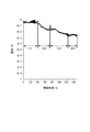
- Example 1 of this invention it is a figure which shows the time-dependent change of the electric current at the time of electrolytic reduction.
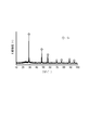
- 1 is an X-ray diffraction pattern of silicon obtained in Example 1 of the present invention. It is a scanning electron micrograph of the silicon obtained in Example 1 of the present invention.
- Example 5 of this invention it is a figure which shows the time-dependent change of the electric current at the time of electrolytic reduction.
- Examples 6 to 8 of the present invention it is a diagram showing the change with time of current during electrolytic reduction.
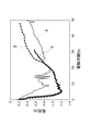
- Examples 9 to 11 of the present invention it is a diagram showing a change with time of current during electrolytic reduction. It is a schematic explanatory drawing of the electrolytic reduction apparatus used for the manufacturing method of the conventional silicon
- the method for producing silicon of the present invention is a method for producing silicon by electrolytic reduction of silicon dioxide in the presence of a molten salt, in which silicon dioxide is placed on a cathode made of silicon. The silicon dioxide is subjected to electrolytic reduction.
- silicon dioxide is used as a raw material.
- silicon dioxide include quartz, silicon dioxide sand, and amorphous silicon dioxide, but the present invention is not limited to such examples.
- amorphous silicon dioxide is preferred because of its high reduction rate.
- the amorphous silicon dioxide include amorphous silicon dioxide contained in diatomaceous earth. In general, diatomaceous earth contains amorphous silicon dioxide at a content of 80 to 90% by mass, but also contains, for example, clay components such as alumina.
- Amorphous silicon dioxide contained in diatomaceous earth unlike crystalline silicon dioxide contained in quartz and the like, has the property of being easily dissolved in an alkaline aqueous solution, so that amorphous silicon dioxide is dissolved in an alkaline aqueous solution. Thereafter, by repeating the operation of precipitating amorphous silicon dioxide by controlling the pH of the aqueous solution, amorphous silicon dioxide having a high purity of 99.9999% by mass or more can be prepared.
- the purity of silicon dioxide is preferably as high as possible from the viewpoint of producing silicon having high purity by electrolytic reduction of silicon dioxide.
- the content of impurities in silicon dioxide is preferably 100 ppm or less, more preferably 10 ppm or less, still more preferably 1 ppm or less, and particularly preferably 0. 0 ppm from the viewpoint of producing silicon having high purity by electrolytic reduction of silicon dioxide. 5 ppm or less.
- Examples of impurities in silicon dioxide include metals such as sodium, potassium, calcium, magnesium, aluminum, titanium, manganese, and iron, boron, phosphorus, and the like, but the present invention is limited to such examples. It is not a thing.
- Silicon dioxide is usually used as silicon dioxide particles.
- the lower limit of the particle diameter of the silicon dioxide particles is preferably 0.2 ⁇ m or more, more preferably 0.5 ⁇ m or more from the viewpoint of efficiently performing the electrolytic reduction of silicon dioxide, and the upper limit of the particle diameter of the silicon dioxide particles is From the viewpoint of efficiently carrying out the electrolytic reduction of silicon dioxide as in the above lower limit, it is preferably 2 ⁇ m or less.
- Silicon dioxide particles can be easily obtained commercially, for example, by refined SiO 2 particles manufactured by Taiheiyo Cement Co., Ltd.
- porous material for silicon dioxide used for electrolytic reduction it is preferable to use a porous material for silicon dioxide used for electrolytic reduction.
- a porous body the molded object shape
- Examples of the shape of the silicon dioxide molded body include a cylinder, a cube, a rectangular parallelepiped, a plate, a thin film, a sphere, and the like, but the present invention is not limited to only such examples.
- the size of the silicon dioxide molded body is not particularly limited, but from the viewpoint of efficiently performing electrolytic reduction of silicon dioxide, a cylindrical molded body having a diameter of about 5 to 30 mm and a thickness of about 1 to 10 mm. A cubic or cuboid shaped body having a side length of about 5 to 30 mm is preferred.
- the silicon dioxide molded body can be easily manufactured by, for example, compression molding.
- a silicon dioxide molded body is produced by compression molding, a porous molded body in which voids communicating with the surface are present inside the molded body is obtained. Since this porous molded body can be impregnated with the molten salt, the porous molded body has the advantage that the electrolytic reduction of silicon dioxide can be performed efficiently. Therefore, in the present invention, a porous molded body of silicon dioxide can be suitably used as silicon dioxide.
- a porous molded body of silicon dioxide can be produced, for example, by mixing silicon dioxide particles and an appropriate amount of water, filling the resulting mixture into a mold having a desired inner surface shape, and pressurizing. .
- the temperature is about 1000 to 1500 ° C. in an air atmosphere or an inert gas atmosphere such as nitrogen gas or argon gas. By heating to sinter, a sintered porous molded body can be produced.
- the porosity of the porous molded body of silicon dioxide is preferably 30% or more, more preferably 40% or more, and still more preferably, from the viewpoint of increasing the efficiency of electrolytic reduction of silicon dioxide by allowing molten salt to enter the inside. From the viewpoint of increasing the mechanical strength of the porous molded body itself and increasing the mechanical strength of silicon generated by electrolytic reduction of silicon dioxide, it is preferably 80% or less, more preferably 70% or less. More preferably, it is 65% or less.
- the particle size of the silicon dioxide particles is the sum of the electrical contact resistance generated between the silicon particles that are reduced and formed while being properly placed on the cathode, suppressing the scattering of particles due to convection in the molten salt. From the viewpoint of improving the electrolytic reduction efficiency of silicon dioxide by reducing the value, it is preferably 50 ⁇ m or more, more preferably 100 ⁇ m or more, still more preferably 200 ⁇ m or more, and even more preferably 300 ⁇ m or more. From the viewpoint of reducing the time required for the electrolytic reduction until, it is preferably 30 mm or less, more preferably 10 mm or less, and even more preferably 3 mm or less.
- the particle diameter of the silicon dioxide granular material is a value measured by a laser diffraction particle size distribution analyzer (manufactured by Nikkiso Co., Ltd., trade name: Microtrac MT3300II, solvent: water, dispersant: none). . Since voids exist between the particles constituting the granular material, the silicon dioxide granular material can be impregnated with the molten salt to the inside thereof, like the porous molded body of silicon dioxide. In addition, there is an advantage that the electrolytic reduction of silicon dioxide can be performed efficiently. Therefore, in the present invention, silicon dioxide particles can be suitably used as silicon dioxide.
- the silicon dioxide granules are produced, for example, by mixing silicon dioxide particles and an appropriate amount of water, filling the resulting mixture into a mold having a desired inner surface shape, pressurizing, and grinding if necessary. be able to.
- sintering the granular material after drying the granular material, by heating to a temperature of about 1000 to 1500 ° C. in an air atmosphere or an inert gas atmosphere such as nitrogen gas or argon gas, Sintered granules can be produced.
- the granular material may be a granular material pulverized after sintering.
- the granular material may be screened to make the particle diameter uniform.
- the present invention has one major feature in that silicon dioxide is electrolytically reduced in the presence of molten salt in a state where silicon dioxide is placed on a cathode made of silicon.
- silicon dioxide is electrolytically reduced in the presence of molten salt in a state where silicon dioxide is placed on a cathode made of silicon.
- a cathode made of silicon is used as the cathode.
- the cathode made of silicon means a cathode having at least a surface formed of silicon. Therefore, the cathode made of silicon may be composed only of silicon, or may be a composite in which the surface of a metal substrate such as molybdenum is covered with silicon. If necessary, silicon dioxide powder may be attached to the surface of the cathode.
- the purity of silicon used for the cathode is preferably 99.9% by mass or more, more preferably 99.99% by mass or more, and further preferably 99.999% by mass or more, from the viewpoint of increasing the purity of the obtained silicon. Especially preferably, it is 99.9999 mass% or more.
- the size of the cathode on which silicon dioxide is placed is not particularly limited as long as silicon dioxide can be placed on the cathode.
- silicon dioxide shaped bodies when one or a plurality of silicon dioxide shaped bodies are used as silicon dioxide, a size that allows any of the shaped bodies to be placed on the cathode is selected. Therefore, the size of the cathode is preferably determined as appropriate according to the size and number of silicon dioxides placed on the cathode.
- the shape of the cathode is not particularly limited, and examples of the shape of the cathode include a disk shape whose planar shape is a circle or an ellipse, a plate shape whose plane shape is a triangle, a rectangle, and other polygons. However, the present invention is not limited to such examples.
- the surface of the cathode on which silicon dioxide is placed preferably has a shape having a large contact area with silicon dioxide from the viewpoint of efficiently performing electrolytic reduction of silicon dioxide.
- the surface of the cathode on which silicon dioxide is placed is preferably planar.
- an uneven shape may be provided on the upper surface of the cathode on which silicon dioxide is placed, and a shape corresponding to the uneven shape may be formed on the bottom surface of the silicon dioxide molded body.
- the cathode is connected to a conductor, for example, and is connected to a power source via the conductor.
- Examples of the salt used for the molten salt include metal halides such as alkali metal halides and alkaline earth metal halides, but the present invention is not limited to such examples. These metal halides may be used alone or in combination of two or more.
- examples of the alkali metal include lithium, sodium, potassium, cesium and the like.
- examples of the alkaline earth metal include magnesium, calcium, strontium, barium and the like.
- a halogen atom which comprises a halide a fluorine atom, a chlorine atom, a bromine atom, an iodine atom etc. are mentioned, for example.
- the metal halide examples include alkali metal halides such as lithium chloride, sodium chloride, potassium chloride, and cesium chloride, and alkaline earth metal halides such as magnesium chloride, calcium chloride, strontium chloride, and barium chloride.
- alkali metal halides such as lithium chloride, sodium chloride, potassium chloride, and cesium chloride
- alkaline earth metal halides such as magnesium chloride, calcium chloride, strontium chloride, and barium chloride.
- the present invention is not limited to such examples.
- These metal halides may be used alone or in combination of two or more.
- lithium oxide, sodium chloride, magnesium chloride, and calcium chloride are preferable, and calcium chloride is more preferable because of high solubility of oxide ions.
- the temperature of the molten salt when electrolytically reducing silicon dioxide is preferably 500 ° C. or higher, more preferably 800 ° C. or higher, from the viewpoint of increasing the reduction efficiency of silicon dioxide. From the viewpoint of suppressing volatilization, it is usually preferably 1000 ° C. or lower, more preferably 900 ° C. or lower.
- anode examples include a carbon electrode, a graphite electrode, a glassy carbon electrode, a ferrite-based insoluble anode, and a titanium boride-based insoluble anode.
- the present invention is not limited to such examples.
- insoluble anodes such as ferrite-based insoluble anodes and titanium boride-based insoluble anodes are preferable from the viewpoint of avoiding contamination with impurities.
- the cathode potential at the time of electrolytic reduction of silicon dioxide so that the potential is higher than the potential at which cations derived from the molten salt precipitate from the melt.
- the cathodic potential differs depending on the type of the molten salt, and thus cannot be determined unconditionally. However, from the viewpoint of avoiding the bond between the metal generated by reduction of the cation derived from the molten salt and silicon, it is generally 0. 5V [vs.
- M n + / M (M is an alkali metal or alkaline earth metal deposited at the cathode limit of the molten salt, n is a valence of the alkali metal or alkaline earth metal)] or higher, preferably 0 more preferably .6V [(the M and n the same as) to M n + / M] is at least, from the viewpoint 1.2V [vs. M n + / M (M and n to improve the efficiency of electrolytic reduction and the The same)] is preferred.
- silicon dioxide is placed on the cathode, molten salt is placed in this electrolytic cell, and electrolytic reduction is performed. Silicon can be produced. At that time, when silicon dioxide is electrolytically reduced while supplying silicon dioxide on the cathode so that silicon dioxide is placed on the cathode, silicon can be continuously produced. It can be efficiently manufactured in large quantities.
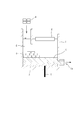
- FIG. 1 is a schematic explanatory view showing an embodiment of the electrolytic reduction apparatus used in the method for producing silicon of the present invention.
- a silicon dioxide plate 2 is disposed on the bottom of the inner surface of the electrolytic cell 1, and a cathode 3 made of silicon is disposed on the silicon dioxide plate 2.
- the electrolytic cell 1 is preferably formed of, for example, quartz or the like from the viewpoint of avoiding impurities from being mixed into generated silicon.
- the silicon dioxide plate 2 is preferably used from the viewpoint of improving the productivity of silicon, but in the present invention, silicon can be easily produced without using the silicon dioxide plate 2.
- the internal space of the electrolytic cell 1 is preferably replaced with an inert gas such as nitrogen gas or argon gas, for example.
- a silicon dioxide 4 is placed on the cathode 3.
- the present invention has one major feature in that the silicon dioxide 4 is electrolytically reduced while the silicon dioxide 4 is placed on the cathode 3.
- silicon dioxide can be continuously electrolytically reduced without taking the complicated operation of replacing the cathode with a new cathode after electrolytic reduction as in the prior art. Silicon can be produced efficiently.
- the silicon dioxide 4 shown in FIG. 1 has a pellet shape, but the present invention is not limited by the shape of the silicon dioxide 4.
- the silicon dioxide 4 is preferably brought into contact with the cathode 3 so that the contact area with the cathode 3 is as large as possible from the viewpoint of efficiently producing silicon. Therefore, it is preferable to place the silicon dioxide 4 on the cathode 3 so that the silicon dioxide 4 and the cathode 3 are in surface contact.
- a molten salt 5 is injected into the electrolytic cell 1, and the molten salt 5 is electrically connected to the cathode 3 in order to electrically connect the anode 6, the cathode 3 and a power source (not shown).
- the body 7 and the reference electrode 8 are immersed.
- the reference electrode 8 is used as necessary.
- the temperature of the molten salt 5 can be measured using a thermocouple (not shown) such as a chromel-alumel thermocouple, for example.
- FIG. 2 is a schematic explanatory view showing another embodiment of the electrolytic reduction apparatus used in the method for producing silicon of the present invention.
- a cathode 3 made of silicon is disposed at the bottom of the inner surface of the electrolytic cell 1.
- the electrolytic cell 1 is preferably formed of, for example, quartz or the like from the viewpoint of avoiding impurities from being mixed into generated silicon.
- the internal space of the electrolytic cell 1 is preferably replaced with an inert gas such as nitrogen gas or argon gas, for example.
- the silicon dioxide 4 is placed on the cathode 3.
- silicon dioxide 4 is electrolytically reduced with the silicon dioxide 4 placed on the cathode 3.
- silicon dioxide 4 is electrolytically reduced to generate silicon 9.
- silicon 9 is generated by adding silicon dioxide 4 further.
- the silicon dioxide 4 is placed on the cathode 3 via
- the silicon dioxide 4 may be placed directly on the cathode 3 so as to be in contact with the cathode 3, or on the cathode 3 through the generated silicon 9 as shown in FIG. 2. It may be placed.
- the produced silicon 9 can be recovered from the take-out port 1a, for example, by providing a take-out port 1a at the lower part of the electrolytic cell 1.
- silicon 9 produced by electrolytic reduction of silicon dioxide 4 while supplying silicon dioxide 4 from the upper part of electrolytic cell 1 is disposed at the lower part of electrolytic cell 1. Since the silicon dioxide 4 can be continuously electrolytically reduced because it can be recovered from the outlet 1a, the silicon 9 can be continuously and efficiently manufactured.
- the silicon dioxide 4 shown in FIG. 2 has the shape of a pellet like the silicon dioxide 4 shown in FIG. 1, the present invention is not limited by the shape of the silicon dioxide 4.
- the silicon dioxide 4 is preferably brought into contact with the cathode 3 so that the contact area with the cathode 3 is as large as possible from the viewpoint of efficiently producing the silicon 9. Therefore, in the embodiment shown in FIG. 2, it is preferable to place the silicon dioxide 4 on the cathode 3 or the produced silicon 9 so that the silicon dioxide 4 is in surface contact with the cathode 3 or the produced silicon 9.
- the molten salt 5 is injected into the electrolytic cell 1.
- the anode 6 is disposed on the upper part of the electrolytic cell 1, but may not necessarily be disposed on the upper part of the electrolytic cell 1, and may be immersed in the molten salt 5.
- the cathode 3 is electrically connected to a power source (not shown) through a conductor 7.
- the temperature of the molten salt 5 can be measured using a thermocouple (not shown) such as a chromel-alumel thermocouple, for example.
- a reference electrode (not shown) may be used as necessary, similarly to the embodiment shown in FIG.
- the anode 6 is immersed in the molten salt 5 in the molten salt 5 and the molten salt 5 is immersed in the molten salt.
- the silicon 9 can be manufactured efficiently. Further, new silicon dioxide 4 is supplied to the molten salt 5 from the upper part of the electrolytic cell 1 while recovering the generated silicon 9 from the outlet 1 a disposed at the lower part of the electrolytic cell 1, and the silicon dioxide 4 on the cathode 3. Therefore, the silicon 9 can be manufactured continuously and efficiently.
- the content of metal impurities in the silicon produced as described above is preferably 100 mass ppm (hereinafter referred to as “ppm”) when used for applications requiring high purity such as silicon for solar cells. ) Or less, more preferably 10 ppm or less, further preferably 1 ppm or less, still more preferably 0.5 ppm or less, and particularly preferably 0.1 ppm or less.
- ppm 100 mass ppm
- metal impurities include sodium, magnesium, aluminum, potassium, calcium, titanium, manganese, iron, and the like, but the present invention is not limited to such examples.
- the properties of a p-type semiconductor or an n-type semiconductor are added to silicon by adding an additive such as boron or phosphorus to silicon in a small amount. Can be granted.
- the total content of boron and phosphorus contained in silicon is preferably 1 ppm or less from the viewpoint of controlling the function as a semiconductor.
- the silicon obtained by the production method of the present invention as described above is useful, for example, as a photovoltaic power element for solar cells, a negative electrode material for lithium batteries, and a raw material for silicon compounds.
- Example 1 Raw material of molten salt As a raw material of molten salt, 400 g of calcium chloride (purity: 99% or more) was placed in a quartz crucible (inner diameter: 85 mm, height: 120 mm, thickness: 2.5 mm), and then 500 The product from which moisture was removed by vacuum drying at 1 ° C. for 1 day or longer was used.
- Silicon dioxide As silicon dioxide used in the electrolytic reduction, both were mixed at a rate of 1.5 g of water per 1 g of silicon dioxide powder (manufactured by Taiheiyo Cement Co., Ltd., refined silica powder), and the resulting mixture was obtained. A pellet having an outer diameter of 12 mm and a thickness of 3 mm was prepared by putting it in a mold and pressurizing it at a pressure of 1.5 ⁇ 10 3 kg / cm 2 (about 147 MPa), and then in an argon gas atmosphere at 1350 ° C. Silicon dioxide pellets obtained by sintering for 30 minutes at temperature were used.
- Electrolytic reduction operation and results thereof Electrolytic reduction of silicon dioxide was performed using the electrolytic reduction apparatus shown in FIG.
- Argon gas (purity: 99.995%) was allowed to flow into the internal space of the quartz electrolytic cell 1, and the inside of the electrolytic cell 1 was maintained in an argon gas atmosphere.
- the silicon dioxide pellets obtained above as silicon dioxide 4 are placed on the cathode 3, and the molten salt 5 of calcium chloride heated and melted at 850 ° C. is put in the electrolytic cell 1 in an amount of 400 g.
- Constant potential electrolysis was carried out at a potential of 0.8 V (vs.
- FIG. 3 shows changes with time in the current during electrolytic reduction.
- the reduced part of the pellet was recovered and its X-ray diffraction was examined.
- X-ray diffraction was measured using an X-ray diffractometer (trade name: Ultimate IV, manufactured by Rigaku Corporation) with CuK ⁇ rays at a wavelength ( ⁇ ) of 1.5418 mm, a voltage of 40 kV, and a current of 40 mA.
- the X-ray diffraction pattern is shown in FIG.
- FIG. 5 As shown in the scanning electron micrograph of FIG. 5, a needle-like structure having a diameter of about 1 ⁇ m, a columnar structure having a diameter of about 10 ⁇ m, and a lump structure in which particles are aggregated were confirmed in the silicon obtained above. Moreover, when elemental analysis of each region of X 1 , X 2, and X 3 shown in FIG. 5 was performed with an X-ray analyzer [trade name: Genesis, manufactured by EDAX], needle-like and columnar substances were Was also confirmed to be silicon. On the other hand, a large amount of oxygen was detected from the massive portion, suggesting that a relatively large amount of silicon dioxide was contained. From the above, it was confirmed that silicon having a needle-like or columnar structure was formed by electrolytic reduction of silicon dioxide as described above.
- the molybdenum content was less than 0.1 ppm
- the boron content was less than 1 ppm
- the phosphorus content was 1 ppm. Was less than.
- FIG. 2 shows an electrolytic reduction apparatus that can easily supply silicon dioxide continuously.
- An electrolytic reduction apparatus was used.
- silicon dioxide 4 the same silicon dioxide pellets as used in Example 1 were used. While conducting the electrolytic reduction of silicon dioxide 4 in the same manner as in Example 1, silicon dioxide pellets were put into the molten calcium chloride salt 5 from the upper part of the electrolytic cell 1 so that the silicon dioxide 4 was placed on the cathode 3. By doing so, the silicon dioxide 4 was supplied on the cathode 3, and the silicon dioxide 4 was electrolytically reduced.
- the silicon dioxide pellets were initially floating in the vicinity of the bath surface of the calcium chloride molten salt 5, but settled in the calcium chloride molten salt 5 after a while. Thereafter, in the same manner as in Example 1, when constant potential electrolysis was performed at a potential of 0.8 V (vs. Ca 2+ / Ca) for 58 hours, the amount of electricity supplied was the electricity required to reduce silicon dioxide 4. About 80% of the amount.
- the produced silicon was recovered from the outlet 1a disposed in the lower part of the electrolytic cell 1, washed in the same manner as in Example 1, and then the X-ray diffraction of the produced silicon 9 was examined.
- the diffraction lines derived from were clearly observed. Therefore, when the silicon dioxide 4 is electrolytically reduced while supplying the silicon dioxide 4 onto the cathode 3 so that the silicon dioxide 4 is placed on the cathode 3, the silicon 9 is continuously and efficiently supplied. It was confirmed that it could be manufactured.
- the content of impurities contained in the obtained silicon 9 was examined by glow discharge mass spectrometry, the content of molybdenum was less than 0.1 ppm, the content of boron was less than 1 ppm, and the content of phosphorus was 1 ppm. Was less than.
- Comparative Example 1 Silicon was produced according to the description in “Example 1” of JP-A-2006-321688. At that time, it is necessary to produce a cathode in which the silicon electrode and the porous silicon dioxide powder compact are in contact with each other by attaching the porous silicon dioxide powder compact to the silicon electrode rod. The operation was complicated. In addition, after electrolytic reduction of silicon dioxide, the cathode must be taken out of the electrolytic cell and replaced with a new cathode, so that the operation is complicated and the operation of electrolytic reduction of silicon dioxide must be temporarily interrupted. I had to.
- Example 1 and Example 2 as compared with Comparative Example 1, the complicated operation of attaching the porous silicon dioxide powder compact to the silicon electrode rod is unnecessary. It can be seen that can be efficiently electrolytically reduced. Moreover, according to Example 1 and Example 2, since silicon dioxide can be continuously supplied in an electrolytic cell and silicon can be manufactured continuously, it can be seen that silicon can be manufactured efficiently. Furthermore, according to Example 2, the silicon dioxide can be electrolytically reduced while supplying silicon dioxide onto the cathode so that silicon dioxide is placed on the cathode, and the generated silicon can be recovered. Since silicon can be produced continuously and efficiently, it can be seen that silicon can be produced continuously in large quantities.
- Example 3 In Example 1, electrolytic reduction was performed in the same manner as in Example 1 except that the cathode potential was changed from 0.8 V (vs. Ca 2+ / Ca) to 1.2 V (vs. Ca 2+ / Ca). . As a result, it was confirmed that silicon having a low impurity content can be efficiently produced as in Example 1.
- Example 4 In Example 2, electrolytic reduction was performed in the same manner as in Example 2 except that the cathode potential was changed from 0.8 V (vs. Ca 2+ / Ca) to 1.2 V (vs. Ca 2+ / Ca). . As a result, it was confirmed that silicon having a low impurity content can be produced as in Example 2 and that silicon can be produced continuously and efficiently.
- Example 5 In Example 1, except that the cathode potential was changed from 0.8 V (vs. Ca 2+ / Ca) to 0.7 V (vs. Ca 2+ / Ca) and the electrolysis time was changed from 150 hours to 80 hours.
- the electrolytic reduction was performed in the same manner as in Example 1.
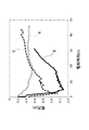
- FIG. 6 shows changes with time in the current during electrolytic reduction.
- the broken line indicates the change over time of the current during electrolytic reduction when the cathode potential is 0.7 V (vs. Ca 2+ / Ca) (Example 5)
- the solid line indicates that the cathode potential is 0.8 V (vs. Ca 2+ / Ca) shows the time-dependent change of the current during electrolytic reduction (Example 1).
- the reduction current (Example 5) during electrolysis when the cathode potential is 0.7 V (vs. Ca 2+ / Ca) shows that the cathode potential is 0.8 V (vs. Ca). 2 + / Ca), which is larger than the reduction current during electrolysis (Example 1), the reduction rate when the cathode potential is 0.7 V (vs. Ca 2+ / Ca) is It can be seen that the reduction rate is higher than that when the cathode potential is 0.8 V (vs. Ca 2+ / Ca). Further, according to Example 5, it was confirmed that silicon having a low impurity content can be efficiently produced as in Example 1.
- Examples 6-8 The silicon dioxide pellets used in Example 1 were pulverized, and the obtained pulverized product was sieved to obtain silicon dioxide granular materials having a particle diameter of 500 ⁇ m to 1 mm.
- Example 1 instead of placing silicon dioxide pellets on the cathode 3 as the silicon dioxide 4, placing the silicon dioxide particles obtained above on the cathode 3, and setting the cathode potential to 0.8V (Vs. Ca 2+ / Ca) to 0.7 V (vs. Ca 2+ / Ca) (Example 6), 0.6 V (vs. Ca 2+ / Ca) (Example 7) or 0.5 V (vs. Ca 2 + / Ca) (Example 8) and the electrolysis time was changed from 150 hours to 50 hours (Example 6), 48 hours (Example 7) or 31 hours (Example 8), Electrolytic reduction was carried out in the same manner as in Example 1.
- FIG. 7 shows changes with time in the current during electrolytic reduction.
- FIG. 7 shows changes with time in the current during electrolytic reduction.
- A is the time-dependent change in current during electrolytic reduction when the cathode potential is 0.7 V (vs. Ca 2+ / Ca)
- B is the cathode potential is 0.6 V (vs. Ca 2). + / Ca)
- the time-dependent change in current during electroreduction (Example 7)
- C is the time-dependent change in current during electroreduction when the cathode potential is 0.5 V (vs. Ca 2+ / Ca) (Example 8) is shown.
- Examples 9-11 Silicon dioxide powder (manufactured by Taiheiyo Cement Co., Ltd., refined silica powder) is mixed at a rate of 1.5 g of water per gram, and the resulting mixture is sintered at a temperature of 1350 ° C. for 30 minutes in an argon gas atmosphere. Thus, a silicon dioxide granular material was obtained. The obtained silicon dioxide granules are sieved to obtain silicon dioxide granules having a particle diameter of 5 to 7 mm (Example 9), silicon dioxide granules having a particle diameter of 500 ⁇ m to 1 mm (Example 10), and a particle diameter of 250 to 500 ⁇ m. Of silicon dioxide (Example 11) was obtained.
- Example 1 instead of placing silicon dioxide pellets as the silicon dioxide 4 on the cathode 3, the silicon dioxide granular material having a particle diameter of 5 to 7 mm obtained above (Example 9), obtained above.
- the silicon dioxide granular material having a particle diameter of 500 ⁇ m to 1 mm (Example 10) or the silicon dioxide granular material having a particle diameter of 250 to 500 ⁇ m obtained above (Example 11) was placed on the cathode 3, and the cathode potential was changed. Change from 0.8 V (vs. Ca 2+ / Ca) to 0.5 V (vs.
- FIG. 8 shows changes with time in the current during electrolytic reduction.
- A is the time-dependent change in current during electrolytic reduction when using silicon dioxide granules having a particle diameter of 5 to 7 mm (Example 9)
- B is silicon dioxide granules having a particle diameter of 500 ⁇ m to 1 mm.
- C shows the time-dependent change in current during electrolytic reduction (Example 11) when using silicon dioxide particles having a particle diameter of 250 to 500 ⁇ m.
- the silicon production method of the present invention it is not necessary to take out the cathode from the electrolytic cell after electrolytic reduction of silicon dioxide, and silicon can be produced by continuously electrolytic reduction of silicon dioxide. I understand.
Landscapes
- Chemical & Material Sciences (AREA)
- Organic Chemistry (AREA)
- Inorganic Chemistry (AREA)
- Engineering & Computer Science (AREA)
- Chemical Kinetics & Catalysis (AREA)
- Electrochemistry (AREA)
- Materials Engineering (AREA)
- Metallurgy (AREA)
- Electrolytic Production Of Non-Metals, Compounds, Apparatuses Therefor (AREA)
- Silicon Compounds (AREA)
- Electrolytic Production Of Metals (AREA)
Abstract
La présente invention concerne un procédé de production de silicium consistant à réduire électrolytiquement du dioxyde de silicium en présence de sel fondu. Le procédé est caractérisé en ce que le dioxyde de silicium est placé sur une cathode composée de silicium et en ce que le dioxyde de silicium dans cet état est réduit électrolytiquement.
Applications Claiming Priority (2)
| Application Number | Priority Date | Filing Date | Title |
|---|---|---|---|
| JP2011-120042 | 2011-05-30 | ||
| JP2011120042 | 2011-05-30 |
Publications (1)
| Publication Number | Publication Date |
|---|---|
| WO2012165017A1 true WO2012165017A1 (fr) | 2012-12-06 |
Family
ID=47258883
Family Applications (1)
| Application Number | Title | Priority Date | Filing Date |
|---|---|---|---|
| PCT/JP2012/058210 Ceased WO2012165017A1 (fr) | 2011-05-30 | 2012-03-28 | Procédé de production de silicium |
Country Status (3)
| Country | Link |
|---|---|
| JP (1) | JP6025140B2 (fr) |
| TW (1) | TW201247937A (fr) |
| WO (1) | WO2012165017A1 (fr) |
Cited By (3)
| Publication number | Priority date | Publication date | Assignee | Title |
|---|---|---|---|---|
| US20150050816A1 (en) * | 2013-08-19 | 2015-02-19 | Korea Atomic Energy Research Institute | Method of electrochemically preparing silicon film |
| CN106591891A (zh) * | 2016-12-09 | 2017-04-26 | 武汉大学 | 一种将致密材料制备成纳米多孔材料的方法 |
| WO2021008579A1 (fr) * | 2019-07-17 | 2021-01-21 | 武汉大学 | Matériau composite de silicium-carbone hautement dispersé, son procédé de préparation et son application |
Families Citing this family (6)
| Publication number | Priority date | Publication date | Assignee | Title |
|---|---|---|---|---|
| KR101642026B1 (ko) * | 2013-08-19 | 2016-07-22 | 한국원자력연구원 | 전기화학적 실리콘 막 제조방법 |
| JP6559538B2 (ja) * | 2015-10-26 | 2019-08-14 | 株式会社東芝 | ガラス固化体の溶解方法及びその溶解装置 |
| WO2017073330A1 (fr) * | 2015-10-27 | 2017-05-04 | 新日鐵住金株式会社 | Procédé de production de plaque métallique revêtue de silicium |
| KR102208279B1 (ko) * | 2019-05-22 | 2021-01-27 | 충북대학교 산학협력단 | 리튬이차전지 음극소재용 다공성 실리콘의 제조방법 |
| RU2717780C1 (ru) * | 2019-10-22 | 2020-03-25 | Федеральное государственное бюджетное учреждение науки Институт химии твердого тела Уральского отделения Российской академии наук | Способ получения волокнистого кремния |
| WO2022118326A1 (fr) * | 2020-12-06 | 2022-06-09 | Helios Project Ltd | Procédé de préparation de silicium |
Citations (3)
| Publication number | Priority date | Publication date | Assignee | Title |
|---|---|---|---|---|
| JP2002517613A (ja) * | 1998-06-05 | 2002-06-18 | ケンブリッジ ユニヴァーシティ テクニカル サービスイズ リミティッド | 溶融塩中での電気分解による金属酸化物および固溶体からの酸素の除去 |
| JP2006321688A (ja) * | 2005-05-19 | 2006-11-30 | Kyoto Univ | シリコンの製造方法 |
| JP2009529607A (ja) * | 2006-03-10 | 2009-08-20 | エルケム アクシエセルスカプ | 金属の電解製造及び精練方法 |
Family Cites Families (2)
| Publication number | Priority date | Publication date | Assignee | Title |
|---|---|---|---|---|
| JP4513297B2 (ja) * | 2003-09-30 | 2010-07-28 | 日本軽金属株式会社 | 金属酸化物の還元方法及び金属酸化物の還元装置 |
| JP2011098861A (ja) * | 2009-11-06 | 2011-05-19 | Toshiba Corp | 太陽電池用シリコンの製造方法及び製造装置 |
-
2012
- 2012-03-28 WO PCT/JP2012/058210 patent/WO2012165017A1/fr not_active Ceased
- 2012-03-28 JP JP2012074754A patent/JP6025140B2/ja not_active Expired - Fee Related
- 2012-03-28 TW TW101110733A patent/TW201247937A/zh unknown
Patent Citations (3)
| Publication number | Priority date | Publication date | Assignee | Title |
|---|---|---|---|---|
| JP2002517613A (ja) * | 1998-06-05 | 2002-06-18 | ケンブリッジ ユニヴァーシティ テクニカル サービスイズ リミティッド | 溶融塩中での電気分解による金属酸化物および固溶体からの酸素の除去 |
| JP2006321688A (ja) * | 2005-05-19 | 2006-11-30 | Kyoto Univ | シリコンの製造方法 |
| JP2009529607A (ja) * | 2006-03-10 | 2009-08-20 | エルケム アクシエセルスカプ | 金属の電解製造及び精練方法 |
Cited By (4)
| Publication number | Priority date | Publication date | Assignee | Title |
|---|---|---|---|---|
| US20150050816A1 (en) * | 2013-08-19 | 2015-02-19 | Korea Atomic Energy Research Institute | Method of electrochemically preparing silicon film |
| CN106591891A (zh) * | 2016-12-09 | 2017-04-26 | 武汉大学 | 一种将致密材料制备成纳米多孔材料的方法 |
| WO2021008579A1 (fr) * | 2019-07-17 | 2021-01-21 | 武汉大学 | Matériau composite de silicium-carbone hautement dispersé, son procédé de préparation et son application |
| US11489164B2 (en) | 2019-07-17 | 2022-11-01 | Wuhan University | Highly dispersed silicon-carbon solid sol, preparation method and application thereof |
Also Published As
| Publication number | Publication date |
|---|---|
| JP6025140B2 (ja) | 2016-11-16 |
| TW201247937A (en) | 2012-12-01 |
| JP2013011012A (ja) | 2013-01-17 |
Similar Documents
| Publication | Publication Date | Title |
|---|---|---|
| JP6025140B2 (ja) | シリコンの製造方法 | |
| CN109417194A (zh) | 锂二次电池用硫化物系固体电解质 | |
| JP2018135602A (ja) | シリコンナノ粒子の製造方法 | |
| CN106978612A (zh) | 一种金属化合物的冶金方法 | |
| Toba et al. | Electrolytic reduction of SiO2 granules in molten CaCl2 | |
| CN101545111A (zh) | 一种单质硅的制备方法 | |
| CN101457372A (zh) | 一种含钛废渣直接制备钛及钛合金的方法 | |
| CN104733702B (zh) | 一种熔盐电解制备纳米硅碳复合负极材料的装置及方法 | |
| JP4765066B2 (ja) | シリコンの製造方法 | |
| KR101185836B1 (ko) | 금속산화물로부터 금속을 제조하기 위한 전해환원공정 | |
| RU2692759C1 (ru) | Свинцово-углеродный металлический композиционный материал для электродов свинцово-кислотных аккумуляторов и способ его синтеза | |
| CN101743342A (zh) | 从切割剩余物回收元素硅的方法 | |
| CN114182301B (zh) | 一种氟化物熔盐电解氧化铍制备金属铍的方法 | |
| JP2007016293A (ja) | 懸濁電解による金属の製造方法 | |
| CN115161714B (zh) | 一种熔盐固态脱氧法制取金属钛的方法 | |
| CN203644876U (zh) | 一种熔盐电解制备纳米硅碳复合负极材料的装置 | |
| KR20100071571A (ko) | 탄화티타늄 제조방법 | |
| WO2008041007A1 (fr) | Procédé et appareil pour produire des poudres métalliques | |
| CN104831306A (zh) | 超细硅基合金粉体及其电化学制备方法 | |
| CN107793144A (zh) | 导电性钙铝石型化合物块体的制备方法 | |
| KR20130060664A (ko) | 전해정련법에 의한 고순도 실리콘 나노섬유의 제조방법 | |
| JP2014111801A (ja) | 溶融塩電解によるシリコンの製造法 | |
| KR100684404B1 (ko) | LiCl-Li₂O 용융염계에서 산화물 핵연료의전기화학적 금속전환반응에 사용되는 봉형Fe₃O₄양극의 제조방법 및 이를 이용한 전기 화학적금속전환 셀 | |
| JP6222067B2 (ja) | 陽極の再生方法、水酸化インジウム粉の製造方法、酸化インジウム粉の製造方法、及びスパッタリングターゲットの製造方法 | |
| Zhao et al. | Electrochemical evaluation of titanium production from porous Ti2O3 in LiCl-KCl-Li2O eutectic melt |
Legal Events
| Date | Code | Title | Description |
|---|---|---|---|
| 121 | Ep: the epo has been informed by wipo that ep was designated in this application |
Ref document number: 12793862 Country of ref document: EP Kind code of ref document: A1 |
|
| NENP | Non-entry into the national phase |
Ref country code: DE |
|
| 122 | Ep: pct application non-entry in european phase |
Ref document number: 12793862 Country of ref document: EP Kind code of ref document: A1 |