WO2012165504A1 - 酸化物超電導薄膜、超電導限流器及び酸化物超電導薄膜の製造方法 - Google Patents
酸化物超電導薄膜、超電導限流器及び酸化物超電導薄膜の製造方法 Download PDFInfo
- Publication number
- WO2012165504A1 WO2012165504A1 PCT/JP2012/063988 JP2012063988W WO2012165504A1 WO 2012165504 A1 WO2012165504 A1 WO 2012165504A1 JP 2012063988 W JP2012063988 W JP 2012063988W WO 2012165504 A1 WO2012165504 A1 WO 2012165504A1
- Authority
- WO
- WIPO (PCT)
- Prior art keywords
- thin film
- substrate
- superconducting
- intermediate layer
- layer
- Prior art date
- Legal status (The legal status is an assumption and is not a legal conclusion. Google has not performed a legal analysis and makes no representation as to the accuracy of the status listed.)
- Ceased
Links
Images




Classifications
-
- H—ELECTRICITY
- H10—SEMICONDUCTOR DEVICES; ELECTRIC SOLID-STATE DEVICES NOT OTHERWISE PROVIDED FOR
- H10N—ELECTRIC SOLID-STATE DEVICES NOT OTHERWISE PROVIDED FOR
- H10N60/00—Superconducting devices
- H10N60/80—Constructional details
- H10N60/85—Superconducting active materials
- H10N60/855—Ceramic superconductors
- H10N60/857—Ceramic superconductors comprising copper oxide
- H10N60/858—Ceramic superconductors comprising copper oxide having multilayered structures, e.g. superlattices
-
- C—CHEMISTRY; METALLURGY
- C30—CRYSTAL GROWTH
- C30B—SINGLE-CRYSTAL GROWTH; UNIDIRECTIONAL SOLIDIFICATION OF EUTECTIC MATERIAL OR UNIDIRECTIONAL DEMIXING OF EUTECTOID MATERIAL; REFINING BY ZONE-MELTING OF MATERIAL; PRODUCTION OF A HOMOGENEOUS POLYCRYSTALLINE MATERIAL WITH DEFINED STRUCTURE; SINGLE CRYSTALS OR HOMOGENEOUS POLYCRYSTALLINE MATERIAL WITH DEFINED STRUCTURE; AFTER-TREATMENT OF SINGLE CRYSTALS OR A HOMOGENEOUS POLYCRYSTALLINE MATERIAL WITH DEFINED STRUCTURE; APPARATUS THEREFOR
- C30B25/00—Single-crystal growth by chemical reaction of reactive gases, e.g. chemical vapour-deposition growth
- C30B25/02—Epitaxial-layer growth
-
- C—CHEMISTRY; METALLURGY
- C30—CRYSTAL GROWTH
- C30B—SINGLE-CRYSTAL GROWTH; UNIDIRECTIONAL SOLIDIFICATION OF EUTECTIC MATERIAL OR UNIDIRECTIONAL DEMIXING OF EUTECTOID MATERIAL; REFINING BY ZONE-MELTING OF MATERIAL; PRODUCTION OF A HOMOGENEOUS POLYCRYSTALLINE MATERIAL WITH DEFINED STRUCTURE; SINGLE CRYSTALS OR HOMOGENEOUS POLYCRYSTALLINE MATERIAL WITH DEFINED STRUCTURE; AFTER-TREATMENT OF SINGLE CRYSTALS OR A HOMOGENEOUS POLYCRYSTALLINE MATERIAL WITH DEFINED STRUCTURE; APPARATUS THEREFOR
- C30B29/00—Single crystals or homogeneous polycrystalline material with defined structure characterised by the material or by their shape
- C30B29/10—Inorganic compounds or compositions
- C30B29/16—Oxides
- C30B29/22—Complex oxides
- C30B29/225—Complex oxides based on rare earth copper oxides, e.g. high T-superconductors
-
- H—ELECTRICITY
- H10—SEMICONDUCTOR DEVICES; ELECTRIC SOLID-STATE DEVICES NOT OTHERWISE PROVIDED FOR
- H10N—ELECTRIC SOLID-STATE DEVICES NOT OTHERWISE PROVIDED FOR
- H10N60/00—Superconducting devices
- H10N60/01—Manufacture or treatment
- H10N60/0268—Manufacture or treatment of devices comprising copper oxide
- H10N60/0296—Processes for depositing or forming copper oxide superconductor layers
- H10N60/0576—Processes for depositing or forming copper oxide superconductor layers characterised by the substrate
- H10N60/0604—Monocrystalline substrates, e.g. epitaxial growth
-
- H—ELECTRICITY
- H10—SEMICONDUCTOR DEVICES; ELECTRIC SOLID-STATE DEVICES NOT OTHERWISE PROVIDED FOR
- H10N—ELECTRIC SOLID-STATE DEVICES NOT OTHERWISE PROVIDED FOR
- H10N60/00—Superconducting devices
- H10N60/01—Manufacture or treatment
- H10N60/0268—Manufacture or treatment of devices comprising copper oxide
- H10N60/0296—Processes for depositing or forming copper oxide superconductor layers
- H10N60/0576—Processes for depositing or forming copper oxide superconductor layers characterised by the substrate
- H10N60/0632—Intermediate layers, e.g. for growth control
-
- H—ELECTRICITY
- H10—SEMICONDUCTOR DEVICES; ELECTRIC SOLID-STATE DEVICES NOT OTHERWISE PROVIDED FOR
- H10N—ELECTRIC SOLID-STATE DEVICES NOT OTHERWISE PROVIDED FOR
- H10N60/00—Superconducting devices
- H10N60/30—Devices switchable between superconducting and normal states
-
- H—ELECTRICITY
- H10—SEMICONDUCTOR DEVICES; ELECTRIC SOLID-STATE DEVICES NOT OTHERWISE PROVIDED FOR
- H10N—ELECTRIC SOLID-STATE DEVICES NOT OTHERWISE PROVIDED FOR
- H10N60/00—Superconducting devices
- H10N60/01—Manufacture or treatment
- H10N60/0268—Manufacture or treatment of devices comprising copper oxide
- H10N60/0296—Processes for depositing or forming copper oxide superconductor layers
- H10N60/0324—Processes for depositing or forming copper oxide superconductor layers from a solution
Definitions
- the present invention relates to an oxide superconducting thin film, a superconducting fault current limiter, and a method for manufacturing an oxide superconducting thin film.
- the oxide superconductor to be deposited is represented by, for example, a composition formula of RE-based superconductor (RE: rare earth element) that exhibits a superconducting phenomenon at a liquid nitrogen temperature (77 K) or higher, particularly YBa 2 Cu 3 O 7- ⁇ .
- RE rare earth element
- YBCO Yttrium-based superconductors
- Such oxide superconducting thin films using RE-based superconductors are expected to be applied to superconducting current limiters, cables, and SMES (superconducting energy storage devices), and much attention is paid to RE-based superconductors and their manufacturing methods. Collecting.
- Jc characteristic a critical current density characteristic (hereinafter referred to as Jc characteristic) is one of the factors that impede the practical application of oxide superconducting materials (particularly oxide superconducting thin films) including RE superconductors. ) Is not easy to improve. For example, in order to put a superconducting fault current limiter using an oxide superconducting thin film into practical use, it is required to pass a current as large as possible with zero resistance. To that end, it is necessary to improve the Jc characteristics of the oxide superconducting thin film.
- Patent Document 1 Japanese Patent Laid-Open No. 2005-2905278 discloses a buffer layer (intermediate layer) made of CeO 2 or the like on a substrate cut and polished by shifting from the r-plane or a-plane of a sapphire single crystal by several degrees. And a method of manufacturing an oxide superconducting thin film that improves the Jc characteristics of the oxide superconducting thin film by forming a superconducting layer made of an RE-based superconductor or the like.
- the oxide superconductor crystal itself has an electric anisotropy in which electricity easily flows in the a-axis direction and the b-axis direction of the crystal axis, but hardly flows in the c-axis direction. . Therefore, when an oxide superconductor is formed on a substrate, it is necessary to orient the a-axis or b-axis in the direction in which electricity flows and to orient the c-axis in other directions.
- the present invention has been made in view of the above-described facts, and provides an oxide superconducting thin film, a superconducting fault current limiter, and a method of manufacturing an oxide superconducting thin film that improve Jc characteristics and suppress the decrease in n-value characteristics. With the goal.
- An oxide superconducting thin film comprising: a layer; and a superconducting layer formed on the intermediate layer and containing, as a main component, an oxide superconductor that is c-axis oriented in a direction perpendicular to the surface of the intermediate layer.
- ⁇ 2> The oxide superconducting thin film according to ⁇ 1>, wherein an angle formed between the main surface of the substrate and the crystal plane of the single crystal structure is 2 degrees or more and 15 degrees or less.
- the oxide superconductor is represented by a composition formula REBa 2 Cu 3 O 7- ⁇ (RE is a single rare earth element or a plurality of rare earth elements, and ⁇ is an oxygen non-stoichiometric amount).
- RE is a single rare earth element or a plurality of rare earth elements, and ⁇ is an oxygen non-stoichiometric amount.
- ⁇ 1> or ⁇ 2> The oxide superconducting thin film according to ⁇ 1>.
- ⁇ 4> The oxide superconducting thin film according to ⁇ 3>, wherein the substrate is a sapphire substrate, the crystal plane is an r-plane or an a-plane, and the intermediate layer is made of CeO 2 or REMnO 3. .
- the substrate is a rectangular parallelepiped, and the side surface of the substrate is cut substantially parallel to the line of intersection between the crystal plane and the main surface of the substrate, and any one of ⁇ 1> to ⁇ 4>
- a superconducting fault current limiter comprising: a superconducting current limiting element comprising an electrode formed on the superconducting layer of the oxide superconducting thin film and connected to the current introduction / exit section in the sealed container.
- ⁇ 7> a step of cutting a substrate having a single crystal structure at an angle from a crystal plane of the single crystal structure, and a thin intermediate layer having a thickness of 10 nm to 40 nm is deposited on the cut surface of the substrate And a step of annealing at a high temperature of 700 ° C. or more and 950 ° C. or less and a step of forming a superconducting layer on the intermediate layer at a growth rate faster in the a-axis direction than in the c-axis direction. Thin film manufacturing method.
- the growth rate in the a-axis direction is set to 15 to 25 times the growth rate in the c-axis direction. Production method.
- an oxide superconducting thin film a superconducting fault current limiter, and a method for manufacturing an oxide superconducting thin film that improve the Jc characteristic and suppress the decrease in the n-value characteristic.
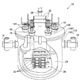
- FIG. 1 is a schematic configuration diagram of a superconducting fault current limiter according to an embodiment of the present invention.
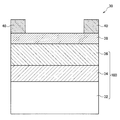
- FIG. 2 is a diagram showing a cross-sectional structure of the thin film superconducting element according to the embodiment of the present invention.
- FIG. 3 is a diagram for explaining the crystal structure of each component of the oxide superconducting thin film shown in FIG.
- FIG. 4 is a diagram showing the crystal structure of sapphire.
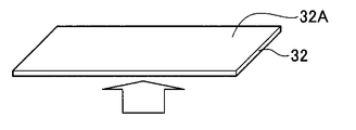
- FIG. 5A is a process diagram of a method for manufacturing an oxide superconducting thin film according to an embodiment of the present invention.
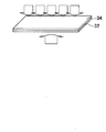
- FIG. 5B is a process diagram of the manufacturing method of the oxide superconducting thin film following FIG. 5A.
- FIG. 5C is a process diagram of the manufacturing method of the oxide superconducting thin film following FIG.
- FIG. 5D is a process diagram of the manufacturing method of the oxide superconducting thin film following FIG. 5C.
- FIG. 5E is a process diagram of the manufacturing method of the oxide superconducting thin film following FIG. 5D.
- FIG. 5F is a process diagram of the manufacturing method of the oxide superconducting thin film subsequent to FIG. 5E.
- FIG. 1 is a schematic configuration diagram of a superconducting fault current limiter 10 according to an embodiment of the present invention.
- the superconducting fault current limiter 10 uses a superconducting-normal state transitions (S / N transition) of a superconductor, and normally has zero resistance and an overcurrent exceeding a critical current flows. This is a device with high resistance and a function to suppress overcurrent.
- the superconducting fault current limiter 10 includes a sealed container 12 that is sealed by closing a container body 12A with a lid 12B.
- a refrigerator 14 is connected to the container body 12 ⁇ / b> A, and liquid nitrogen is introduced into the sealed container 12 from the refrigerator 14.
- the lid 12B is connected to a current introduction / extraction portion 16 that introduces and flows out current from the outside to the inside of the sealed container 12.
- the current introduction / extraction unit 16 is configured by a three-phase AC circuit, and specifically includes three current introduction units 16A and three current outflow units 16B corresponding thereto.
- Each of the current introduction portion 16A and the current outflow portion 16B includes a conducting wire 18 that penetrates the lid 12B and extends in the vertical direction, and a cylindrical body 20 that covers the conducting wire 18.
- One end of the conducting wire 18 of the current introduction portion 16A exposed to the outside is connected to one end of the corresponding conducting wire 18 of the current outflow portion 16B exposed to the outside via an external resistor 22 as a shunt resistor.
- An element storage container 24 is supported on an end portion of each cylindrical body 20 inside the container main body 12A.
- the element storage container 24 is built in the sealed container 12 and cooled to the inside by liquid nitrogen filled in the sealed container 12.
- a current limiting unit 26 composed of a plurality of thin film superconducting elements 30 is incorporated.
- the current limiting unit 26 is configured by three sets in which the thin film superconducting elements 30 are arranged in four rows and two columns.
- This current limiting unit 26 is supported by the other end inside the conducting wire 18 of the current introducing portion 16A, the other end inside the conducting wire 18 of the current outflow portion 16B, and the support column 28, and is a three-phase alternating current.
- the other end inside the conducting wire 18 of the current introducing portion 16A and the other end inside the conducting wire 18 of the current outflow portion 16B are electrically connected via the thin film superconducting element 30 so as to constitute a circuit. It is connected to the.
- FIG. 2 is a diagram showing a cross-sectional structure of the thin film superconducting element 30 according to the embodiment of the present invention.
- the thin film superconducting element 30 has a laminated structure in which an intermediate layer 34, a superconducting layer 36, and a protective layer 38 are sequentially formed on a substrate 32.
- a pair of electrodes 40 that are electrically connected to the conductive wire 18 described above are disposed.
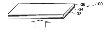
- the substrate 32, the intermediate layer 34, and the superconducting layer 36 in FIG. 2 constitute the oxide superconducting thin film 100 according to the embodiment of the present invention.
- the substrate 32 has a single crystal structure of metal oxide or ceramic.
- Various shapes can be adopted as the shape of the substrate 32 on the assumption that there is a main surface on which the superconducting layer 36 and the intermediate layer 34 are formed, but it is preferable to adopt a rectangular flat plate shape that is easy to handle.
- the metal oxide include Al 2 O 3 (aluminum oxide, particularly sapphire), (Zr, Y) O 2 (yttria stabilized zirconia), LaAlO 3 (lanthanum aluminate), SrTiO 3 (strontium titanate).
- (La x Sr 1-x ) (Al x Ta 1-x ) O 3 lanthanum strontium tantalum aluminum oxide), NdGaO 3 (neodymium gallate), YAlO 3 (yttrium aluminate), MgO (magnesium oxide), TiO 2 (Titania), BaTiO 3 (barium titanate) and the like.
- Ceramics include silicon carbide and graphite. In particular, among these, it is preferable to employ a sapphire substrate because it does not break even when exposed to a rapid temperature change when used as a current limiting element.
- substrate 32 is not specifically limited, For example, it is 1 mm.
- the intermediate layer 34 is a layer formed on the substrate 32 in order to achieve high in-plane orientation in the superconducting layer 36, and may be composed of a single layer film or a multilayer film.
- the intermediate layer 34 is not particularly limited, and is made of a substance having self-orientation. This substance is, for example, a substance selected from CeO 2 and REMnO 3 , preferably CeO 2 .
- the film thickness of the intermediate layer 34 is not particularly limited, but is 20 nm, for example.
- the superconducting layer 36 is formed on the intermediate layer 34 and is made of an oxide superconductor, preferably a copper oxide superconductor.
- the copper oxide superconductor can be configured by combining these crystal materials.
- RE in REBa 2 Cu 3 O 7- ⁇ is a single rare earth element or a plurality of rare earth elements such as Y, Nd, Sm, Eu, Gd, Dy, Ho, Er, Tm, Yb and Lu, Among these, Y is preferable because it is difficult to cause substitution with the Ba site.
- ⁇ is an oxygen nonstoichiometric amount, for example, 0 or more and 1 or less, and is preferably closer to 0 from the viewpoint of a high superconducting transition temperature.
- the oxygen non-stoichiometric amount may be less than 0, that is, take a negative value when high-pressure oxygen annealing or the like is performed using an apparatus such as an autoclave.
- ⁇ of the crystal material other than REBa 2 Cu 3 O 7- ⁇ represents an oxygen non - stoichiometric amount, for example, 0 or more and 1 or less.
- the film thickness of the oxide superconducting layer 36 is not particularly limited, but is, for example, 200 nm.
- the protective layer 38 is made of silver or the like. Although the film thickness of the protective layer 38 is not specifically limited, For example, it is 200 nm.
- the pair of electrodes 40 is composed of a conductive member such as a gold-silver alloy.
- Table 1 is a table showing the relationship between the crystal structure (growth direction) of each component and each characteristic.
- “ ⁇ ” indicates that the corresponding value is high
- “X” indicates that the corresponding value is low
- “ ⁇ ” indicates that the corresponding value is between “O” and “X”.
- the “off-cut present” substrate in the table is a substrate cut at an angle from the crystal plane of the single crystal structure constituting the substrate 32, that is, a crystal plane having an angle with respect to the main surface of the substrate. Means a substrate having a single crystal structure.
- “No off-cut” in the table indicates a normal substrate that has not been cut.
- “axial growth” in the table means that growth is performed so as to be axially oriented in a direction perpendicular to the crystal plane of the single crystal structure constituting the substrate 32 with offcut.
- plane growth means that the intermediate layer is grown so as to be axially oriented in a direction perpendicular to the cut surface (main surface) of the single crystal structure constituting the substrate 32 with offcut.
- the superconducting layer it means that it is grown so as to be c-axis oriented in the direction perpendicular to the surface of the intermediate layer.
- the intermediate layer has an island shape because the bonding force inside the intermediate layer is small and the surface energy is small, and it is difficult to form an oxide superconducting layer.
- the Jc characteristic is high (see Patent Document 1). This Jc characteristic is considered to be improved by the fact that the difference in lattice constant between the intermediate layer and the superconducting layer is relaxed by the off-cut, and the lattice strain generated between the intermediate layer and the superconducting layer is reduced.
- the intermediate layer grown in the axial direction is formed on the substrate with “off-cut”, and the oxide superconducting layer grown in the axial direction is formed on the intermediate layer.
- the oxide superconducting layer if an electric current is caused to flow horizontally with respect to the cut surface of the substrate, the c-axis of the oxide superconductor that is difficult to pass electricity is not perpendicular to the direction of the current. It becomes difficult for current to flow horizontally to the surface. Thereby, it is considered that the n-value characteristic is deteriorated as compared with the case 1 of the prior art.
- an intermediate layer grown in the axial direction is formed on the “off-cut” substrate, and the surface is formed on the intermediate layer. A directionally grown oxide superconducting layer is formed.
- the oxide superconducting layer when an electric current is made to flow horizontally with respect to the cut surface of the substrate, the c-axis of the oxide superconductor that is difficult to conduct electricity is perpendicular to the direction of the current. It becomes easy for current to flow horizontally with respect to the cut surface. Thereby, it is considered that the decrease of the n-value characteristic can be suppressed while improving the Jc characteristic.
- FIG. 3 is a diagram for explaining the crystal structure of each component of the oxide superconducting thin film 100 shown in FIG.
- FIG. 4 is a diagram showing the crystal structure (unit cell) of sapphire.
- a-plane, r-plane, and c-plane indicate lattice planes, and their mirror indices are shown in parentheses.
- the substrate 32 is a substrate in which a predetermined crystal surface 32A having a single crystal structure has an angle ⁇ from the substrate main surface 32B.
- the substrate is formed by cutting a substrate base material having a predetermined crystal plane 32A having a single crystal structure at an angle ⁇ from the surface and polishing the cut surface.
- the crystal surface 32A is the r-plane or a-plane (see FIG. 4)
- the cut surface 32B is the r-plane.
- the cut surface 32B has a c-axis of the oxide superconductor perpendicular to the direction of the current, and is 2 from the r-plane or the a-plane in order to make the current flow more horizontally with respect to the cut surface of the substrate. It is preferable to have an angle of at least degrees.
- the cut surface 32B becomes the main surface of the substrate 32, and the intermediate layer 34 is formed on the cut surface 32B.
- the side surface of the substrate 32 is cut substantially parallel to the intersection line between the crystal surface 32A (actually a surface obtained by extending the crystal surface) and the substrate main surface 32B. Preferably it is.
- the side surface of the superconducting layer 36 is also substantially parallel to the intersecting line.
- the direction of the current flowing through the layer 36 is substantially the same direction as the intersecting line.
- the substrate 32 can reduce the c-axis of the oxide superconductor existing in the direction in which the current flows, that is, the c-axis of the oxide superconductor can be made perpendicular to the direction of the current.
- substantially parallel means not only “parallel” but also a parallel direction including an angle of about ⁇ 3 degrees from “parallel”.
- the intermediate layer 34 is formed on the cut surface 32B (substrate main surface), and a predetermined axis of crystal is oriented in a direction perpendicular to the crystal surface 32A.
- the intermediate layer 34 is made of CeO 2.
- the a-axis grows in the axial direction, that is, in the direction perpendicular to the crystal plane 32A on the cut surface 32B.
- the “vertical direction” includes not only perpendicular to the crystal plane 32A but also an angle of about ⁇ 5 degrees from the vertical.
- the intermediate layer 34 is made of a material other than CeO 2
- the axial orientation in the direction perpendicular to the crystal plane 32A is not limited to the a-axis.
- the superconducting layer 36 is formed on the intermediate layer 34 and contains an oxide superconductor whose c-axis 36A is oriented in a direction perpendicular to the surface of the intermediate layer 34 as a main component.
- an oxide superconductor whose c-axis 36A is oriented in a direction perpendicular to the surface of the intermediate layer 34 as a main component.
- YBCO is adopted as the material of the superconducting layer 36
- YBCO is grown on the surface of the intermediate layer 34 in the surface direction.
- the “vertical direction” includes not only vertical to the surface of the intermediate layer 34 but also an angle of about ⁇ 5 degrees from the vertical.
- the “main component” indicates that the content is the largest among the constituent components contained in the superconducting layer 36, and preferably has a content of 90% or more.
- the thin film superconducting element 30 or the oxide superconducting thin film 100 according to the embodiment of the present invention it is possible to improve the Jc characteristic and suppress the decrease in the n-value characteristic.
- FIG. 5 is a process diagram of the method for manufacturing the oxide superconducting thin film 100 according to the embodiment of the present invention.
- a substrate base material cutting step is performed.
- a single crystal substrate base material 200 such as a sapphire substrate having a predetermined crystal plane 32A as a main surface is prepared, and the single crystal substrate base material 200 is in-plane with an angle ⁇ from the predetermined crystal plane 32A.
- the substrate 32 having a rectangular flat plate shape is obtained by cutting in the direction.
- the cut surface 32B of the substrate 32 is polished to improve surface flatness.
- a pre-annealing step is performed.
- the polished substrate 32 is pre-annealed within a temperature range of, for example, 1000 ° C. or more and 1200 ° C. or less. This pre-annealing step can be omitted as appropriate.
- an intermediate layer forming step is performed.
- the method for forming the intermediate layer 34 include a PLD (Pulse Laser Deposition) method, a CVD (Chemical Vapor Deposition) method, a MOCVD (Metal Organic Chemical Vapor Deposition) method, an IBAD (Ion Beam Assisted Deposition) method, and a TFA-MOD (Tri Fluoro Acetates-Metal Organic Deposition) method, sputtering method, electron beam evaporation method or the like can be used.
- a highly efficient film formation can be realized.
- intermediate layer forming step for example, when an electron beam evaporation method is used, plasma is generated in oxygen of 1 ⁇ 10 ⁇ 4 Pa to 1 ⁇ 10 ⁇ 1 Pa and the substrate 32 is heated to 700 ° C. or higher.
- An intermediate layer 34 is formed by depositing a film made of CeO 2 or the like on the cut surface 32B of the substrate 32 by about 10 nm to 40 nm, preferably about 10 nm to 20 nm.
- a post-annealing process is performed.
- the substrate 32 is placed in a temperature range of, for example, 700 ° C. or higher and 950 ° C. or lower, preferably 800 ° C. or higher and 90 ° C. or lower.
- the surface of the intermediate layer 34 is treated by heating at a temperature within a temperature range of 0 ° C. or lower, and the flatness of the surface of the intermediate layer 34 is improved and the material valence of the intermediate layer 34 is controlled.
- an a-axis 34 ⁇ / b> A such as CeO 2 constituting the intermediate layer 34 in the direction perpendicular to the crystal plane 32 ⁇ / b> A of the single crystal structure constituting the substrate 32.
- a superconducting layer forming step is performed.
- the method for forming (depositing) the superconducting layer 36 include a PLD method, a CVD method, a MOCVD method, a MOD method, and a sputtering method.
- the MOD method it is preferable to use the MOD method in that a highly efficient film formation without using a high vacuum can be realized.
- the superconducting layer forming step when the superconducting layer 36 made of YBCO is formed by using, for example, the MOD method, first, as shown in FIG.
- a solution 35 of an organic complex of yttrium, barium, and copper is spin-coated with the intermediate layer 34.
- a precursor film 36A is formed on the surface.
- the precursor film 36A is temporarily fired at, for example, 300 ° C. or more and 600 ° C. or less in the air.
- the film 36A is subjected to main baking at 700 ° C. or more and 900 ° C. or less to obtain a superconducting layer 36 composed of an oxide superconductor of YBCO from the film 36A.
- the superconducting layer 36 (film 36A) is formed at a growth rate faster in the ab plane direction than in the c-axis direction.
- main baking is performed on the film 36A in an inert atmosphere.
- the main firing in an inert atmosphere, the growth in the ab plane direction is promoted, the superconducting layer 36 grows in the so-called plane direction, and the c-axis 36A of YBCO is oriented in the direction perpendicular to the surface of the intermediate layer 34. become.
- this main baking can also be first performed in an inert atmosphere and in the middle in an oxygen atmosphere.
- the growth rate in the a-axis direction is preferably 10 times to 25 times the growth rate in the c-axis direction, preferably 15 times to 25 times. It is more preferable to set it to double or less.
- the case where the cut surface 32B after being cut is polished has been described.
- the polishing can be omitted as appropriate.
- the protective layer 38 can also be omitted as appropriate.
- the oxide superconducting thin film 100 is used as the thin film type superconducting element 30 of the superconducting fault current limiter 10 .
- a long substrate is used as the substrate 32 to obtain a superconducting wire, etc.
- the oxide superconducting thin film 100 can be applied to various other devices.
- the obtained oxide superconducting thin film 100 is widely used for devices such as SMES (Superconducting Magnetic Energy Storage), superconducting transformer, NMR (nuclear magnetic resonance) analyzer, single crystal pulling device, linear motor car, magnetic separation device and the like. Yes.
- oxide superconducting thin film the superconducting fault current limiter, and the manufacturing method of the oxide superconducting thin film according to the present invention will be described with reference to examples, but the present invention is not limited to these examples.
- three thin film superconducting elements used for the superconducting fault current limiter were produced as oxide superconducting thin films.
- Example 1 a thin film type superconducting element 1 provided with the oxide superconducting thin film of Case 3 in Table 1 was prepared.
- a sapphire substrate was prepared.
- the sapphire substrate was pre-annealed at 1000 ° C.
- plasma is generated in oxygen of 1 ⁇ 10 ⁇ 2 Pa or more and 6 ⁇ 10 ⁇ 2 Pa or less using an electron beam evaporation method, and CeO 2 is about 20 nm in sapphire in a state where the sapphire substrate is heated at 750 degrees.
- An intermediate layer was formed by vapor deposition on the main surface (cut surface) of the substrate. Then, the substrate was post-annealed at 800 degrees to perform surface treatment of the intermediate layer.
- a solution of an organic complex of yttrium, barium, and copper was applied onto the surface of the intermediate layer with a spin coater, and pre-baked in air at 500 ° C. Then, main baking was performed at 800 ° C.
- a thin film superconducting element 1 was fabricated by depositing a gold-silver alloy (Au-23 atm% Ag) on the obtained oxide superconducting thin film by sputtering and attaching electrodes.
- the obtained thin film type superconducting element 1 becomes a superconducting state by being cooled to the temperature of liquid nitrogen, but becomes a normal conducting state when a current of a certain level or more flows, and can perform current limiting.
- a thin film superconducting element 2 provided with the oxide superconducting thin film of Case 1 in Table 1 was prepared.
- the intermediate layer and the oxide superconducting layer are formed on the “non-cut-cut” substrate.
- a substrate base material made of a sapphire single crystal is cut in an in-plane direction along the r-plane direction of the single crystal (the angle between the substrate main surface and the r-plane direction of the single crystal is 0, that is, “off-cut non-substrate”), and then a sapphire substrate whose cut surface was polished was prepared.
- the sapphire substrate was pre-annealed at 1000 ° C.
- an intermediate layer and a superconducting layer were formed by the same method as in Example 1.
- a gold-silver alloy Au-23 atm% Ag
- an electrode was attached to produce a thin film superconducting element 2.
- ⁇ Comparative Example 2> a thin film superconducting element 3 provided with the oxide superconducting thin film of Case 2 in Table 1 above was produced. At this time, the angle ⁇ of the cut surface was 8 degrees. The details of the manufacturing method other than the corresponding column in Table 1 are the same as in Example 1.
- Example 2 An intermediate layer and a superconducting layer were formed by the same method as in Example 1. Then, a gold-silver alloy (Au-23 atm% Ag) was formed on the obtained oxide superconducting thin film by a sputtering method, and an electrode was attached to produce a thin film superconducting element 3.
- Au-23 atm% Ag gold-silver alloy
- Example 1 when the pole figure of the obtained sample was measured, it was confirmed that the pole figure of the intermediate layer was tilted in the same direction as the sapphire substrate, whereas the slope of the pole figure of YBCO was small. did it. On the other hand, when the pole figure of the obtained sample is measured in Comparative Example 2, the pole figure of the intermediate layer is inclined in the same direction as the sapphire substrate, and the pole figure of YBCO is also inclined in the same direction as the sapphire substrate. was confirmed.
- Jc characteristic evaluation> The critical current density (Jc) distribution at the liquid nitrogen temperature of the thin film superconducting elements 1 to 3 was measured by an induction method using CRYOSCAN manufactured by THEVA, and the highest Jc among the distributions was evaluated.
- the Jc characteristics of the thin film superconducting elements 1 and 3 of Example 1 and Comparative Example 2 are improved as compared with the thin film superconducting element 2 of Comparative Example 1 in which the substrate is not cut. Can be confirmed.
- the thin film type superconducting element 1 of Example 1 in which the YBCO forming the superconducting layer is grown in the surface direction has lower n-value characteristics.
- the superconducting layer has a lower degree of decrease compared to the thin film type superconducting element 3 of Comparative Example 2 in the axial growth, the superconducting layer is grown in the plane direction instead of in the axial direction. It was confirmed that the decrease in n-value characteristics can be suppressed.
- the angle ⁇ for cutting the substrate base material made of sapphire single crystal from the r-plane direction of the single crystal is adjusted as shown in Table 1, and the sapphire substrate according to Examples 2 to 10 is obtained. Prepared. Otherwise, a thin film superconducting element was formed in the same manner as in Example 1.
- the evaluation criteria were set as follows. ⁇ ⁇ : less than 3MA / cm 3 ⁇ ⁇ : less than 3MA / cm 3 or more 4MA / cm 3 ⁇ ⁇ : 4MA / cm 3 or more
- evaluation criteria were set as follows. ⁇ ⁇ : Less than 10 ⁇ ⁇ : 10 or more and less than 20 ⁇ ⁇ : 20 or more
- the angle ⁇ for cutting the substrate base material made of sapphire single crystal from the r-plane direction of the single crystal is 2 degrees or more, the Jc characteristics are all “ ⁇ ”, and the Ic characteristics are better than other elements. Met. Furthermore, if the angle ⁇ at which the substrate base material made of sapphire single crystal is cut from the r-plane direction of the single crystal is not less than 2 degrees and not more than 10 degrees, not only the Jc characteristics but also the n-value characteristics are all “ ⁇ ”. The Jc characteristic and the n-value characteristic were the best as compared with the element.
- Reference numeral 10 denotes a superconducting current limiting device.
- Reference numeral 12 denotes an airtight container.
- Reference numeral 16 denotes a current introduction / extraction part.
- Reference numeral 24 denotes an element storage container.
- Reference numeral 30 denotes a thin film type superconducting element (superconducting current limiting element).
- Reference numeral 32 denotes a substrate.
- Reference numeral 32A denotes a crystal plane.
- Reference numeral 32B denotes a cut surface and a substrate main surface.
- Reference numeral 34A denotes an axis, the a-axis.
- Reference numeral 34 denotes an intermediate layer.
- Reference numeral 36A denotes a c-axis.
- Reference numeral 36 denotes a superconducting layer.
- Reference numeral 40 denotes an electrode.
- Reference numeral 100 denotes an oxide superconducting thin film.
Landscapes
- Chemical & Material Sciences (AREA)
- Engineering & Computer Science (AREA)
- Crystallography & Structural Chemistry (AREA)
- Organic Chemistry (AREA)
- Materials Engineering (AREA)
- Metallurgy (AREA)
- Manufacturing & Machinery (AREA)
- Inorganic Chemistry (AREA)
- Chemical Kinetics & Catalysis (AREA)
- General Chemical & Material Sciences (AREA)
- Ceramic Engineering (AREA)
- Superconductors And Manufacturing Methods Therefor (AREA)
- Crystals, And After-Treatments Of Crystals (AREA)
Abstract
Jc特性を向上しつつ、n値特性の低下を抑制する。 単結晶構造を有し、当該単結晶構造の結晶面(32A)と基板主面(32B)が角度を有する基板(32)と、基板主面(32B)上に形成され、結晶面(32A)に対して垂直方向に軸配向した中間層(34)と、当該中間層(34)上に形成され、中間層表面に対して垂直方向にc軸配向した酸化物超電導体を主成分として含有する超電導層(36)と、を備える。
Description
本発明は、酸化物超電導薄膜、超電導限流器及び酸化物超電導薄膜の製造方法に関する。
従来から、酸化物超電導材料を実用化するための技術として、基板を用意し、当該基板上に酸化物超電導体を成膜して酸化物超電導薄膜を得る方法がある。
成膜する酸化物超電導体としては、例えば、液体窒素温度(77K)以上で超電導現象を示すRE系超電導体(RE:希土類元素)、特にYBa2Cu3O7-δの組成式で表されるイットリウム系超電導体(以下、「YBCO」と記載する)がよく用いられている。
このようなRE系超電導体を用いた酸化物超電導薄膜は、超電導限流器やケーブル、SMES(超電導エネルギー貯蔵装置)への応用が期待されており、RE系超電導体及びその製法に大いに注目を集めている。
ところが、RE系超電導体を含め、酸化物超電導材料(特に薄膜形成された酸化物超電導薄膜)を実用化するための障害となっている1つの要因として、臨界電流密度特性(以下、Jc特性という)の向上が容易でないことが挙げられる。
例えば、酸化物超電導薄膜を用いた超電導限流器の実用化には、できるだけ大きな電流を抵抗ゼロで流すことが求められ、そのためには、酸化物超電導薄膜のJc特性を向上させる必要がある。
例えば、酸化物超電導薄膜を用いた超電導限流器の実用化には、できるだけ大きな電流を抵抗ゼロで流すことが求められ、そのためには、酸化物超電導薄膜のJc特性を向上させる必要がある。
そこで、特許文献1(特開2005-290528号公報)には、サファイア単結晶のr面又はa面から数度ずらして切断及び研磨した基板上に、CeO2等からなるバッファ層(中間層)と、RE系超電導体等からなる超電導層とを成膜することで、酸化物超電導薄膜のJc特性を向上する酸化物超電導薄膜の製造方法が開示されている。
ここで、酸化物超電導体の結晶自体は、結晶軸のa軸方向とb軸方向には電気を流し易いが、c軸方向には電気を流しにくいという電気的異方性を有している。したがって、基材上に酸化物超電導体を成膜する場合には、電気を流す方向にa軸あるいはb軸を配向させ、c軸をその他の方向に配向させる必要がある。
しかしながら、特許文献1の構成では、結晶軸が傾いた基板上に超電導層を成膜するため、超電導層を構成するRE系超電導体のa軸あるいはb軸が電流の方向に対してずれて、c軸方向にも電流が流れてしまう可能性がある。
このようにc軸方向にも電流が流れると、超電導状態から抵抗状態への遷移の鋭さを示す尺度である所謂n値(電流電圧特性の指数:E∝Jn)が低下してしまう。
このn値は、Jc特性と共に、酸化物超電導薄膜を超電導限流器等に実用化する上で重要な超電導特性の1つであり、n値の低下は上記実用化の障害となる。
このようにc軸方向にも電流が流れると、超電導状態から抵抗状態への遷移の鋭さを示す尺度である所謂n値(電流電圧特性の指数:E∝Jn)が低下してしまう。
このn値は、Jc特性と共に、酸化物超電導薄膜を超電導限流器等に実用化する上で重要な超電導特性の1つであり、n値の低下は上記実用化の障害となる。
本発明は上記事実に鑑みてなされたものであり、Jc特性を向上しつつ、n値特性の低下を抑制した酸化物超電導薄膜、超電導限流器及び酸化物超電導薄膜の製造方法を提供することを目的とする。
本発明の上記課題は下記の手段によって解決された。
<1> 単結晶構造を有し、前記単結晶構造の結晶面と基板主面が角度を有する基板と、前記基板主面上に形成され、前記結晶面に対して垂直方向に軸配向した中間層と、前記中間層上に形成され、前記中間層表面に対して垂直方向にc軸配向した酸化物超電導体を主成分として含有する超電導層と、を備える酸化物超電導薄膜。
<1> 単結晶構造を有し、前記単結晶構造の結晶面と基板主面が角度を有する基板と、前記基板主面上に形成され、前記結晶面に対して垂直方向に軸配向した中間層と、前記中間層上に形成され、前記中間層表面に対して垂直方向にc軸配向した酸化物超電導体を主成分として含有する超電導層と、を備える酸化物超電導薄膜。
<2>前記基板主面と前記単結晶構造の結晶面がなす角度が2度以上15度以下である、<1>に記載の酸化物超電導薄膜。
<3>前記酸化物超電導体は、組成式REBa2Cu3O7-δ(REは単一の希土類元素又は複数の希土類元素であり、前記δは酸素不定比量である)で表される、<1>又は<2>に記載の酸化物超電導薄膜。
<4>前記基板は、サファイア基板であり、前記結晶面は、r面又はa面であり、前記中間層は、CeO2又はREMnO3から構成される、<3>に記載の酸化物超電導薄膜。
<5>前記基板は直方体であり、前記基板の側面は、前記結晶面と前記基板主面の交線に対し略平行に切断されている、<1>~<4>の何れか1つに記載の酸化物超電導薄膜。
<6>内部に液体窒素が充填される密閉容器と、前記密閉容器の外部から内部へ電流を導入して流出する電流導入出部と、<1>~<5>の何れか1つに記載の酸化物超電導薄膜の超電導層上に電極が形成されて構成され、前記密閉容器内の前記電流導入出部に接続される超電導限流素子と、を備える超電導限流器。
<7>単結晶構造を有した基板を、前記単結晶構造の結晶面から角度を有して切断する工程と、前記基板の切断面上に、厚さ10nm以上40nm以下の薄い中間層を蒸着して、700℃以上950℃以下の高温でアニールする工程と、前記中間層上に、c軸方向よりもa軸方向に速い成長速度で超電導層を成膜する工程と、を有する酸化物超電導薄膜の製造方法。
<8>前記超電導層を成膜する工程は、MOD法で成膜する、<7>に記載の酸化物超電導薄膜の製造方法。
<9>前記超電導層を形成する工程では、a軸方向の成長速度をc軸方向の成長速度の15倍以上25倍以下とする、<7>又は<8>に記載の酸化物超電導薄膜の製造方法。
本発明によれば、Jc特性を向上しつつ、n値特性の低下を抑制した酸化物超電導薄膜、超電導限流器及び酸化物超電導薄膜の製造方法を提供することができる。
以下、添付の図面を参照しながら、本発明の実施形態に係る酸化物超電導薄膜、超電導限流器及び酸化物超電導薄膜の製造方法について具体的に説明する。なお、図中、同一又は対応する機能を有する部材(構成要素)には同じ符号を付して適宜説明を省略する。
<超電導限流器>
図1は、本発明の実施形態に係る超電導限流器10の概略構成図である。
図1は、本発明の実施形態に係る超電導限流器10の概略構成図である。
本発明の実施形態に係る超電導限流器10は、超電導体のS/N転移(superconducting-normal state transitions)を利用して、通常時はゼロ抵抗で、臨界電流以上の過電流が流れた時には高抵抗となって過電流を抑制する機能を持つ機器である。
この超電導限流器10は、容器本体12Aを蓋12Bで閉じて密閉される密閉容器12を備えている。
容器本体12Aには、冷凍機14が接続され、冷凍機14から密閉容器12の内部に液体窒素が導入される。蓋12Bには、密閉容器12の外部から内部へ電流を導入して流出する電流導入出部16が接続されている。電流導入出部16は、3相交流回路で構成され、具体的には3つの電流導入部16Aと、これらに対応する3つの電流流出部16Bとを含んで構成されている。
容器本体12Aには、冷凍機14が接続され、冷凍機14から密閉容器12の内部に液体窒素が導入される。蓋12Bには、密閉容器12の外部から内部へ電流を導入して流出する電流導入出部16が接続されている。電流導入出部16は、3相交流回路で構成され、具体的には3つの電流導入部16Aと、これらに対応する3つの電流流出部16Bとを含んで構成されている。
電流導入部16Aと電流流出部16Bは、それぞれ、蓋12Bに対して貫通して垂直方向に伸びた導線18と、当該導線18を被覆する筒体20とで構成される。
電流導入部16Aの導線18のうち外部に露出した一端は、対応する電流流出部16Bの導線18のうち外部に露出した一端と、分流抵抗としての外部抵抗22を介して接続されている。
電流導入部16Aの導線18のうち外部に露出した一端は、対応する電流流出部16Bの導線18のうち外部に露出した一端と、分流抵抗としての外部抵抗22を介して接続されている。
各筒体20の容器本体12A内部にある端部には、素子収容容器24が支持されている。
この素子収容容器24は、密閉容器12に内蔵され、密閉容器12に充填される液体窒素により内部まで冷却される。
この素子収容容器24は、密閉容器12に内蔵され、密閉容器12に充填される液体窒素により内部まで冷却される。
素子収容容器24には、複数の薄膜型超電導素子30で構成された限流ユニット26が内蔵されている。本発明の実施形態では、具体的に、薄膜型超電導素子30が4行2列で配列された組が3組で限流ユニット26を構成している。
この限流ユニット26は、電流導入部16Aの導線18のうち内部にある他端と、電流流出部16Bの導線18のうち内部にある他端と、支柱28で支持されており、3相交流回路を構成するように、電流導入部16Aの導線18のうち内部にある他端と、電流流出部16Bの導線18のうち内部にある他端とが、薄膜型超電導素子30を介して電気的に接続されている。
この限流ユニット26は、電流導入部16Aの導線18のうち内部にある他端と、電流流出部16Bの導線18のうち内部にある他端と、支柱28で支持されており、3相交流回路を構成するように、電流導入部16Aの導線18のうち内部にある他端と、電流流出部16Bの導線18のうち内部にある他端とが、薄膜型超電導素子30を介して電気的に接続されている。
<薄膜型超電導素子の概略>
次に、薄膜型超電導素子30の概略を説明する。
図2は、本発明の実施形態に係る薄膜型超電導素子30の断面構造を示す図である。
次に、薄膜型超電導素子30の概略を説明する。
図2は、本発明の実施形態に係る薄膜型超電導素子30の断面構造を示す図である。
図2に示すように、薄膜型超電導素子30は、基板32上に中間層34、超電導層36、保護層38が順に形成された積層構造を有している。そして、保護層38上には、上述した導線18に電気的に接続される1対の電極40が配置されている。なお、図2における基板32と中間層34と超電導層36が、本発明の実施形態に係る酸化物超電導薄膜100を構成する。
まず、各構成の概略を説明する。
基板32は、金属酸化物やセラミックスの単結晶構造を有している。基板32の形状は、超電導層36や中間層34が形成される主面があることを前提として様々な形状を採用することができるが、取扱いが容易な矩形平板形状を採用することが好ましい。
金属酸化物の具体例としては、Al2O3(酸化アルミニウム、特にサファイア)、 (Zr,Y)O2(イットリア安定化ジルコニア)、LaAlO3(ランタンアルミネート)、SrTiO3(チタン酸ストロンチウム)、(LaxSr1-x)(AlxTa1-x)O3(酸化ランタンストロンチウムタンタルアルミニウム)、NdGaO3(ネオジムガレート)、YAlO3(イットリウムアルミネート)、MgO(酸化マグネシウム)、TiO2(チタニア)、BaTiO3(チタン酸バリウム)等が挙げられる。セラミックスの具体例としては、炭化ケイ素、黒鉛等が挙げられる。
特に、これらの中でも、限流素子として用いる場合に急激な温度変化にさらされても破壊しない点からサファイア基板を採用することが好ましい。
基板32の厚みは、特に限定されないが、例えば1mmとされている。
金属酸化物の具体例としては、Al2O3(酸化アルミニウム、特にサファイア)、 (Zr,Y)O2(イットリア安定化ジルコニア)、LaAlO3(ランタンアルミネート)、SrTiO3(チタン酸ストロンチウム)、(LaxSr1-x)(AlxTa1-x)O3(酸化ランタンストロンチウムタンタルアルミニウム)、NdGaO3(ネオジムガレート)、YAlO3(イットリウムアルミネート)、MgO(酸化マグネシウム)、TiO2(チタニア)、BaTiO3(チタン酸バリウム)等が挙げられる。セラミックスの具体例としては、炭化ケイ素、黒鉛等が挙げられる。
特に、これらの中でも、限流素子として用いる場合に急激な温度変化にさらされても破壊しない点からサファイア基板を採用することが好ましい。
基板32の厚みは、特に限定されないが、例えば1mmとされている。
中間層34は、超電導層36において高い面内配向性を実現するために基板32上に形成される層であり、単層膜で構成されていても多層膜で構成されていてもよい。
この中間層34は、特に限定されないが、自己配向性を有する物質で構成される。この物質は、例えばCeO2及びREMnO3から選ばれる物質であり、好ましくはCeO2である。
中間層34の膜厚は、特に限定されないが、例えば20nmとされている。
この中間層34は、特に限定されないが、自己配向性を有する物質で構成される。この物質は、例えばCeO2及びREMnO3から選ばれる物質であり、好ましくはCeO2である。
中間層34の膜厚は、特に限定されないが、例えば20nmとされている。
超電導層36は、中間層34上に形成され、酸化物超電導体、好ましくは銅酸化物超電導体で構成されている。
銅酸化物超電導体としては、REBa2Cu3O7-δ(RE-123と称す),Bi2Sr2CaCu2O8+δ(BiサイトにPb等をドープしたものも含む),Bi2Sr2Ca2Cu3O10+δ(BiサイトにPb等をドープしたものも含む),(La,Ba)2CuO4-δ,(Ca,Sr)CuO2-δ[CaサイトはBaであってもよい],(Nd,Ce)2CuO4-δ,(Cu,Mo)Sr2(Ce,Y)sCu2O [(Cu,Mo)-12s2と称し、s=1、2、3,4である],Ba(Pb,Bi)O3又はTl2Ba2Can-1CunO2n+4(nは2以上の整数である)等の組成式で表される結晶材料を用いることができる。また、銅酸化物超電導体は、これら結晶材料を組み合わせて構成することもできる。
上記REBa2Cu3O7-δ中のREは、Y、Nd、Sm、Eu、Gd、Dy、Ho、Er、Tm、YbやLuなどの単一の希土類元素又は複数の希土類元素であり、これらの中でもBaサイトと置換が起き難い等の理由でYであることが好ましい。また、δは、酸素不定比量であり、例えば0以上1以下であり、超電導転移温度が高いという観点から0に近いほど好ましい。なお、酸素不定比量は、オートクレーブ等の装置を用いて高圧酸素アニール等を行えば、δは0未満、すなわち、負の値をとることもある。
また、REBa2Cu3O7-δ以外の結晶材料のδも酸素不定比量を表し、例えば0以上1以下である。
酸化物超電導層36の膜厚は、特に限定されないが、例えば200nmとされている。
銅酸化物超電導体としては、REBa2Cu3O7-δ(RE-123と称す),Bi2Sr2CaCu2O8+δ(BiサイトにPb等をドープしたものも含む),Bi2Sr2Ca2Cu3O10+δ(BiサイトにPb等をドープしたものも含む),(La,Ba)2CuO4-δ,(Ca,Sr)CuO2-δ[CaサイトはBaであってもよい],(Nd,Ce)2CuO4-δ,(Cu,Mo)Sr2(Ce,Y)sCu2O [(Cu,Mo)-12s2と称し、s=1、2、3,4である],Ba(Pb,Bi)O3又はTl2Ba2Can-1CunO2n+4(nは2以上の整数である)等の組成式で表される結晶材料を用いることができる。また、銅酸化物超電導体は、これら結晶材料を組み合わせて構成することもできる。
上記REBa2Cu3O7-δ中のREは、Y、Nd、Sm、Eu、Gd、Dy、Ho、Er、Tm、YbやLuなどの単一の希土類元素又は複数の希土類元素であり、これらの中でもBaサイトと置換が起き難い等の理由でYであることが好ましい。また、δは、酸素不定比量であり、例えば0以上1以下であり、超電導転移温度が高いという観点から0に近いほど好ましい。なお、酸素不定比量は、オートクレーブ等の装置を用いて高圧酸素アニール等を行えば、δは0未満、すなわち、負の値をとることもある。
また、REBa2Cu3O7-δ以外の結晶材料のδも酸素不定比量を表し、例えば0以上1以下である。
酸化物超電導層36の膜厚は、特に限定されないが、例えば200nmとされている。
保護層38は、銀等で構成されている。保護層38の膜厚は、特に限定されないが、例えば200nmとされている。1対の電極40は、金銀合金等の導電部材で構成されている。
<薄膜型超電導素子の詳細>
次に、薄膜型超電導素子30の詳細、特に、酸化物超電導薄膜100の各構成の結晶構造について説明する。
表1は、各構成の結晶構造(成長方向)と各特性の関係を示す表である。なお、表中の「○」は対応する値が高いことを示し、「×」は対応する値が低いことを示し、「△」は対応する値が○と×の中間にあることを示す。また、表中の「オフカット有」の基板とは、基板32を構成する単結晶構造の結晶面から角度を有して切断された基板、すなわち、基板主面に対して角度を有する結晶面を持った単結晶構造を有する基板を意味する。表中の「オフカット無」とは、上記切断がされていない通常の基板を示す。
また、本実施形態において、表中の「軸方向成長」とは、オフカット有の基板32を構成する単結晶構造の結晶面に対して垂直方向に軸配向するように成長させることを意味する。また、「面方向成長」とは、中間層に関しては、オフカット有の基板32を構成する単結晶構造の切断面(主面)に対して垂直方向に軸配向するように成長させることを意味し、超電導層に関しては、中間層表面に対して垂直方向にc軸配向するように成長させることを意味する。
次に、薄膜型超電導素子30の詳細、特に、酸化物超電導薄膜100の各構成の結晶構造について説明する。
表1は、各構成の結晶構造(成長方向)と各特性の関係を示す表である。なお、表中の「○」は対応する値が高いことを示し、「×」は対応する値が低いことを示し、「△」は対応する値が○と×の中間にあることを示す。また、表中の「オフカット有」の基板とは、基板32を構成する単結晶構造の結晶面から角度を有して切断された基板、すなわち、基板主面に対して角度を有する結晶面を持った単結晶構造を有する基板を意味する。表中の「オフカット無」とは、上記切断がされていない通常の基板を示す。
また、本実施形態において、表中の「軸方向成長」とは、オフカット有の基板32を構成する単結晶構造の結晶面に対して垂直方向に軸配向するように成長させることを意味する。また、「面方向成長」とは、中間層に関しては、オフカット有の基板32を構成する単結晶構造の切断面(主面)に対して垂直方向に軸配向するように成長させることを意味し、超電導層に関しては、中間層表面に対して垂直方向にc軸配向するように成長させることを意味する。

表1に示すように、従来技術のケース1では、「オフカット無」の基板上に中間層と酸化物超電導層が形成されている。この場合、実用化するためには、n値特性は十分に高いものの、Jc特性はさらなる向上が必要である。オフカット無(角度がゼロ程度)の場合、中間層と超電導層の格子定数の差から中間層と超電導層の間に格子歪が発生し、この歪が超電導素子のJcを低下させると考えられる。
また、ケース4では、「オフカット有」の基板上に面方向成長した中間層が形成されている。この場合、中間層内部の結合力が小さく、表面エネルギーが小さくなるという理由により、中間層が島状となり、酸化物超電導層の形成が困難となる。
一方で、ケース2,3では、「オフカット有」の基板を採用するため、Jc特性は高くなる(特許文献1参照)。このJc特性は、オフカットにより、中間層と超電導層の格子定数の差が緩和され、中間層と超電導層との間で発生する格子歪が小さくなることにより向上すると考えられる。
しかしながら、ケース2では、「オフカット有」の基板上に軸方向成長した中間層が形成され、この中間層上に軸方向成長した酸化物超電導層が形成されている。この場合、酸化物超電導層において、基板の切断面に対して水平に電流を流そうとすると、電気を流しにくい酸化物超電導体のc軸が電流の方向に対して垂直でないため、基板の切断面に対して水平に電流が流れ難くなる。これにより、従来技術のケース1に比べて、n値特性が低下するものと考えられる。
以上のことを考慮して、ケース3の本発明の実施形態に係る薄膜型超電導素子30では、「オフカット有」の基板上に軸方向成長した中間層が形成され、この中間層上に面方向成長した酸化物超電導層が形成されている。この場合、酸化物超電導層において、基板の切断面に対して水平に電流を流そうとすると、電気が流れにくい酸化物超電導体のc軸が電流の方向に対して垂直であるため、基板の切断面に対して水平に電流が流れ易くなる。これにより、Jc特性を向上しつつ、n値特性の低下を抑制することができると考えられる。
また、ケース4では、「オフカット有」の基板上に面方向成長した中間層が形成されている。この場合、中間層内部の結合力が小さく、表面エネルギーが小さくなるという理由により、中間層が島状となり、酸化物超電導層の形成が困難となる。
一方で、ケース2,3では、「オフカット有」の基板を採用するため、Jc特性は高くなる(特許文献1参照)。このJc特性は、オフカットにより、中間層と超電導層の格子定数の差が緩和され、中間層と超電導層との間で発生する格子歪が小さくなることにより向上すると考えられる。
しかしながら、ケース2では、「オフカット有」の基板上に軸方向成長した中間層が形成され、この中間層上に軸方向成長した酸化物超電導層が形成されている。この場合、酸化物超電導層において、基板の切断面に対して水平に電流を流そうとすると、電気を流しにくい酸化物超電導体のc軸が電流の方向に対して垂直でないため、基板の切断面に対して水平に電流が流れ難くなる。これにより、従来技術のケース1に比べて、n値特性が低下するものと考えられる。
以上のことを考慮して、ケース3の本発明の実施形態に係る薄膜型超電導素子30では、「オフカット有」の基板上に軸方向成長した中間層が形成され、この中間層上に面方向成長した酸化物超電導層が形成されている。この場合、酸化物超電導層において、基板の切断面に対して水平に電流を流そうとすると、電気が流れにくい酸化物超電導体のc軸が電流の方向に対して垂直であるため、基板の切断面に対して水平に電流が流れ易くなる。これにより、Jc特性を向上しつつ、n値特性の低下を抑制することができると考えられる。
図3は、図2に示す酸化物超電導薄膜100の各構成の結晶構造について説明する図である。図4は、サファイアの結晶構造(単位格子)を示す図である。図4中のa面,r面,c面は格子面を示し、カッコ内にそのミラー指数を示す。
本実施形態に係る基板32は、単結晶構造の所定の結晶面32Aが基板主面32Bから角度θを有する基板である。具体的には、単結晶構造の所定の結晶面32Aを有する基板母材から当該表面から角度θを有して切断し、切断表面を研磨して形成した基板である。例えば、基板32として単結晶サファイア基板を採用し、超電導層36の材料としてYBCOを採用した場合、上記結晶面32Aをr面又はa面とし(図4参照)、切断面32Bは、当該r面又はa面から15度以下の角度を有していることが好ましい。15度以下とする理由は、YBCOを面方向成長させる場合に、中間層と超電導層との格子の不整合が起こることを抑制するためである。この格子の不整合が生じた場合、超電導層36を中間層34上に平坦に成膜することが困難となる。また、切断面32Bは、酸化物超電導体のc軸を電流の方向に対して垂直とし、基板の切断面に対して水平に電流を、より流し易くするために、r面又はa面から2度以上の角度を有していることが好ましい。
そして、この切断面32Bが基板32の主面となり、切断面32B上に中間層34が形成される。
なお、基板32が直方体(矩形平板形状)の場合、基板32の側面は、結晶面32A(実際には結晶面を延長した面)と基板主面32Bの交線に対し略平行に切断されていることが好ましい。このように電流が超電導層36の長手方向端部から流されるとき、基板36の側面が上記交線に対し略平行であると、超電導層36の側面も上記交線に対し略平行となり、超電導層36に流れる電流の向きが上記交線と略同一方向となる。これにより、基板32は、電流が流れる方向に存在する酸化物超電導体のc軸を減らす、つまり、酸化物超電導体のc軸を電流の方向に対して垂直にすることができる。
なお、「略平行」とは、単に「平行」のみならず、「平行」から±3度程度角度を有する場合を含む平行方向を意味するものとする。
そして、この切断面32Bが基板32の主面となり、切断面32B上に中間層34が形成される。
なお、基板32が直方体(矩形平板形状)の場合、基板32の側面は、結晶面32A(実際には結晶面を延長した面)と基板主面32Bの交線に対し略平行に切断されていることが好ましい。このように電流が超電導層36の長手方向端部から流されるとき、基板36の側面が上記交線に対し略平行であると、超電導層36の側面も上記交線に対し略平行となり、超電導層36に流れる電流の向きが上記交線と略同一方向となる。これにより、基板32は、電流が流れる方向に存在する酸化物超電導体のc軸を減らす、つまり、酸化物超電導体のc軸を電流の方向に対して垂直にすることができる。
なお、「略平行」とは、単に「平行」のみならず、「平行」から±3度程度角度を有する場合を含む平行方向を意味するものとする。
本実施形態に係る中間層34は、切断面32B(基板主面)上に形成され、結晶面32Aに対して垂直方向に結晶の所定軸が配向したものであり、例えば中間層34がCeO2で構成される場合には、切断面32B上においてa軸が軸方向、つまり結晶面32Aに対して垂直方向に成長したものである。なお、上記「垂直方向」とは、結晶面32Aに対して垂直だけでなく、垂直から±5度程度角度を有する場合を含む。また、中間層34がCeO2以外で構成されている場合、結晶面32Aに対して垂直方向に軸配向するのは、a軸に限定されない。
本実施形態に係る超電導層36は、中間層34上に形成され、前記中間層34表面に対して垂直方向にc軸36Aが配向した酸化物超電導体を主成分として含有したものである。例えば、超電導層36の材料としてYBCOを採用した場合には、中間層34の表面上にYBCOが面方向成長したものである。なお、上記「垂直方向」とは、中間層34表面に対して垂直だけでなく、垂直から±5度程度角度を有する場合を含む。また、「主成分」とは、超電導層36に含まれる構成成分中で含有量が最も多いことを示し、好ましくは90%以上の含有量を有する。
以上の構成を備えることにより、本発明の実施形態に係る薄膜型超電導素子30又は酸化物超電導薄膜100によれば、Jc特性を向上しつつ、n値特性の低下を抑制することができる。
<酸化物超電導薄膜の製造方法>
次に、以上のような酸化物超電導薄膜100の製造方法について具体的に説明する。
図5は、本発明の実施形態に係る酸化物超電導薄膜100の製造方法の工程図である。
次に、以上のような酸化物超電導薄膜100の製造方法について具体的に説明する。
図5は、本発明の実施形態に係る酸化物超電導薄膜100の製造方法の工程図である。
-切断工程-
本発明の実施形態に係る酸化物超電導薄膜100の製造方法では、まず、図5Aのように、基板母材の切断工程を行う。この切断工程では、所定の結晶面32Aを主面として持つサファイア基板等の単結晶基板母材200を用意し、単結晶基板母材200を所定の結晶面32Aから角度θを有して面内方向に切断して、矩形平板状の基板32を得る。切断した後、基板32の切断面32Bを表面の平坦性を向上させるために研磨する。
本発明の実施形態に係る酸化物超電導薄膜100の製造方法では、まず、図5Aのように、基板母材の切断工程を行う。この切断工程では、所定の結晶面32Aを主面として持つサファイア基板等の単結晶基板母材200を用意し、単結晶基板母材200を所定の結晶面32Aから角度θを有して面内方向に切断して、矩形平板状の基板32を得る。切断した後、基板32の切断面32Bを表面の平坦性を向上させるために研磨する。
-プレアニール工程-
次に、図5Bに示すように、プレアニール工程を行う。プレアニール工程では、研磨した基板32を、例えば1000℃以上1200℃以下の温度範囲内でプレアニールする。なお、このプレアニール工程は、適宜省略することもできる。
次に、図5Bに示すように、プレアニール工程を行う。プレアニール工程では、研磨した基板32を、例えば1000℃以上1200℃以下の温度範囲内でプレアニールする。なお、このプレアニール工程は、適宜省略することもできる。
-中間層形成工程-
次に、図5Cに示すように、中間層形成工程を行う。中間層34の形成方法としては、例えばPLD(Pulse Laser Deposition)法、CVD(Chemical Vapor Deposition)法、MOCVD(Metal Organic Chemical Vapor Deposition)法、IBAD(Ion Beam Assisted Deposition)法、TFA-MOD(Tri Fluoro Acetates-Metal Organic Deposition)法、スパッタ法、又は電子ビーム蒸着法などを用いることができる。また、高効率の成膜が実現できるという点で電子ビーム蒸着法を用いることが好ましい。
中間層形成工程で、例えば電子ビーム蒸着法を用いる場合、1×10⁻⁴Pa以上1×10⁻¹Pa以下の酸素中でプラズマを発生させ、700度以上に基板32を加熱した状態で当該基板32の切断面32B上にCeO2等からなる膜を10nmから40nm、好ましくは10nmから20nm程度蒸着させて、中間層34を形成する。
次に、図5Cに示すように、中間層形成工程を行う。中間層34の形成方法としては、例えばPLD(Pulse Laser Deposition)法、CVD(Chemical Vapor Deposition)法、MOCVD(Metal Organic Chemical Vapor Deposition)法、IBAD(Ion Beam Assisted Deposition)法、TFA-MOD(Tri Fluoro Acetates-Metal Organic Deposition)法、スパッタ法、又は電子ビーム蒸着法などを用いることができる。また、高効率の成膜が実現できるという点で電子ビーム蒸着法を用いることが好ましい。
中間層形成工程で、例えば電子ビーム蒸着法を用いる場合、1×10⁻⁴Pa以上1×10⁻¹Pa以下の酸素中でプラズマを発生させ、700度以上に基板32を加熱した状態で当該基板32の切断面32B上にCeO2等からなる膜を10nmから40nm、好ましくは10nmから20nm程度蒸着させて、中間層34を形成する。
-ポストアニール工程-
次に、図5Dに示すように、ポストアニール工程を行う。ポストアニール工程では、基板32を例えば700℃以上950℃以下の温度範囲内、好ましくは800℃以上90
0℃以下の温度範囲内の温度で加熱して中間層34表面の処理し、中間層34表面の平坦性の向上と中間層34の材料価数の制御を行う。また、これにより、中間層34が基板32上において所謂軸方向成長し、基板32を構成する単結晶構造の結晶面32Aに対して垂直方向に中間層34を構成するCeO2等のa軸34Aが配向する。
次に、図5Dに示すように、ポストアニール工程を行う。ポストアニール工程では、基板32を例えば700℃以上950℃以下の温度範囲内、好ましくは800℃以上90
0℃以下の温度範囲内の温度で加熱して中間層34表面の処理し、中間層34表面の平坦性の向上と中間層34の材料価数の制御を行う。また、これにより、中間層34が基板32上において所謂軸方向成長し、基板32を構成する単結晶構造の結晶面32Aに対して垂直方向に中間層34を構成するCeO2等のa軸34Aが配向する。
-超電導層形成工程-
次に、図5E及び図5Fに示すように、超電導層形成工程を行う。超電導層36の形成(成膜)方法としては、例えばPLD法、CVD法、MOCVD法、MOD法、又はスパッタ法などが挙げられる。また、高真空を用いない高効率の成膜が実現できるという点でMOD法を用いることが好ましい。
超電導層形成工程で、例えばMOD法を用いてYBCOからなる超電導層36を形成する場合、まず、図5Eに示すように、イットリウム、バリウム、銅の有機錯体の溶液35をスピンコーターで中間層34の表面上に塗布して前駆体の膜36Aを形成する。そして、図5Fに示すように、前駆体の膜36Aを例えば空気中において300℃以上600℃以下で仮焼成する。
仮焼成で有機溶媒を除去した後、膜36Aを700℃以上900℃以下で本焼成して、膜36AからYBCOの酸化物超電導体で構成される超電導層36を得る。
次に、図5E及び図5Fに示すように、超電導層形成工程を行う。超電導層36の形成(成膜)方法としては、例えばPLD法、CVD法、MOCVD法、MOD法、又はスパッタ法などが挙げられる。また、高真空を用いない高効率の成膜が実現できるという点でMOD法を用いることが好ましい。
超電導層形成工程で、例えばMOD法を用いてYBCOからなる超電導層36を形成する場合、まず、図5Eに示すように、イットリウム、バリウム、銅の有機錯体の溶液35をスピンコーターで中間層34の表面上に塗布して前駆体の膜36Aを形成する。そして、図5Fに示すように、前駆体の膜36Aを例えば空気中において300℃以上600℃以下で仮焼成する。
仮焼成で有機溶媒を除去した後、膜36Aを700℃以上900℃以下で本焼成して、膜36AからYBCOの酸化物超電導体で構成される超電導層36を得る。
ここで、本実施形態では、c軸方向よりもab面方向に速い成長速度で超電導層36(膜36A)を成膜する。具体的に、不活性雰囲気中で膜36Aに対して本焼成を行う。不活性雰囲気中で本焼成を行なうことで、ab面方向の成長が促進され、超電導層36が所謂面方向成長し、YBCOのc軸36Aが中間層34表面に対して垂直方向に配向するようになる。
また、この本焼成は、最初に不活性雰囲気中で、途中から酸素雰囲気中で行うこともできる。これにより、所謂面方向成長と酸素アニールが行われたJc特性の良い超電導層36が得られる。
また、成長速度に関しては、Jc特性の向上という観点から、a軸方向(ab面方向)の成長速度をc軸方向の成長速度の10倍以上25倍以下とすることが好ましく、15倍以上25倍以下とすることがより好ましい。
また、この本焼成は、最初に不活性雰囲気中で、途中から酸素雰囲気中で行うこともできる。これにより、所謂面方向成長と酸素アニールが行われたJc特性の良い超電導層36が得られる。
また、成長速度に関しては、Jc特性の向上という観点から、a軸方向(ab面方向)の成長速度をc軸方向の成長速度の10倍以上25倍以下とすることが好ましく、15倍以上25倍以下とすることがより好ましい。
<変形例>
なお、本発明を特定の実施形態について詳細に説明したが、本発明はかかる実施形態に限定されるものではなく、本発明の範囲内にて他の種々の実施形態が可能であることは当業者にとって明らかであり、例えば上述の複数の実施形態は、適宜、組み合わせて実施可能である。また、以下の変形例同士を、適宜、組み合わせてもよい。
なお、本発明を特定の実施形態について詳細に説明したが、本発明はかかる実施形態に限定されるものではなく、本発明の範囲内にて他の種々の実施形態が可能であることは当業者にとって明らかであり、例えば上述の複数の実施形態は、適宜、組み合わせて実施可能である。また、以下の変形例同士を、適宜、組み合わせてもよい。
例えば、図5Aに示す切断工程では、切断した後の切断面32Bを研磨する場合を説明したが、レーザーカット等で表面が平らに切断可能な場合には、適宜研磨は省略することができる。
また、保護層38も適宜省略することができる。
また、保護層38も適宜省略することができる。
また、本実施形態では、酸化物超電導薄膜100を超電導限流器10の薄膜型超電導素子30として用いる場合を説明したが、例えば基板32として長尺のものを用いて、超電導線材を得る等、酸化物超電導薄膜100は他の様々な機器に応用することができる。得られた酸化物超電導薄膜100は、SMES(Superconducting Magnetic Energy Storage)、超電導トランス、NMR(核磁気共鳴)分析装置、単結晶引き上げ装置、リニアモーターカー、磁気分離装置等の機器に広く用いられている。
なお、日本出願2011-122221の開示はその全体が参照により本明細書に取り込まれる。
本明細書に記載された全ての文献、特許出願、および技術規格は、個々の文献、特許出願、および技術規格が参照により取り込まれることが具体的かつ個々に記載された場合と同程度に、本明細書中に参照により取り込まれる。
本明細書に記載された全ての文献、特許出願、および技術規格は、個々の文献、特許出願、および技術規格が参照により取り込まれることが具体的かつ個々に記載された場合と同程度に、本明細書中に参照により取り込まれる。
以下に、本発明に係る酸化物超電導薄膜、超電導限流器及び酸化物超電導薄膜の製造方法について、実施例により説明するが、本発明はこれら実施例により何ら限定されるものではない。
実施例では、酸化物超電導薄膜として、超電導限流器に用いられる薄膜型超電導素子を3つ作製した。
<実施例1>
具体的に、実施例1では、上記表1のケース3の酸化物超電導薄膜を備えた薄膜型超電導素子1を作製した。
薄膜型超電導素子1の作製では、まず、サファイア単結晶からなる基板母材を単結晶のr面方向から角度θ=10度を有して面内方向に切断し、その後、切断面を研磨したサファイア基板を用意した。次に、サファイア基板を1000℃でプレアニールした。
次に、電子ビーム蒸着法を用いて、1×10⁻²Pa以上6×10⁻²Pa以下の酸素中でプラズマを発生させ、750度でサファイア基板を加熱した状態でCeO2を20nm程度サファイア基板の主面(切断面)上に蒸着させて中間層を形成した。そして、基板を800度でポストアニールして、中間層の表面処理を行った。
次に、イットリウム、バリウム、銅の有機錯体の溶液を中間層の表面上にスピンコーターで塗布し、500℃空気中で仮焼成を行なった。そして、不活性雰囲気中800度で本焼成を行ない、途中から酸素雰囲気に切り替えて、最終的にYBCOからなる超電導層を中間層上に形成した。これにより、上記表1のケース3の酸化物超電導薄膜を作製した。
得られた酸化物超電導薄膜に金銀合金(Au-23atm%Ag)をスパッタ法で成膜し、電極を取り付けることで薄膜型超電導素子1を作製した。
具体的に、実施例1では、上記表1のケース3の酸化物超電導薄膜を備えた薄膜型超電導素子1を作製した。
薄膜型超電導素子1の作製では、まず、サファイア単結晶からなる基板母材を単結晶のr面方向から角度θ=10度を有して面内方向に切断し、その後、切断面を研磨したサファイア基板を用意した。次に、サファイア基板を1000℃でプレアニールした。
次に、電子ビーム蒸着法を用いて、1×10⁻²Pa以上6×10⁻²Pa以下の酸素中でプラズマを発生させ、750度でサファイア基板を加熱した状態でCeO2を20nm程度サファイア基板の主面(切断面)上に蒸着させて中間層を形成した。そして、基板を800度でポストアニールして、中間層の表面処理を行った。
次に、イットリウム、バリウム、銅の有機錯体の溶液を中間層の表面上にスピンコーターで塗布し、500℃空気中で仮焼成を行なった。そして、不活性雰囲気中800度で本焼成を行ない、途中から酸素雰囲気に切り替えて、最終的にYBCOからなる超電導層を中間層上に形成した。これにより、上記表1のケース3の酸化物超電導薄膜を作製した。
得られた酸化物超電導薄膜に金銀合金(Au-23atm%Ag)をスパッタ法で成膜し、電極を取り付けることで薄膜型超電導素子1を作製した。
得られた薄膜型超電導素子1は、液体窒素温度まで冷却されることで超電導状態になるが一定以上の電流が流れると常電導状態となり限流を行うことが可能となる。
<比較例1>
比較例1では、上記表1のケース1の酸化物超電導薄膜を備えた薄膜型超電導素子2を作製した。従来技術のケース1では、「オフカット無」の基板上に中間層と酸化物超電導層が形成されている。
薄膜型超電導素子2の作製では、まず、サファイア単結晶からなる基板母材を単結晶のr面方向に沿って面内方向に切断し(基板主面と単結晶のr面方向との角度が0、すなわち「オフカット無」の基板とする)、その後、切断面を研磨したサファイア基板を用意した。次に、サファイア基板を1000℃でプレアニールした。次に、実施例1と同一の方法で中間層と超電導層を形成した。そして、得られた酸化物超電導薄膜に金銀合金(Au-23atm%Ag)をスパッタ法で成膜し、電極を取り付けることで薄膜型超電導素子2を作製した。
比較例1では、上記表1のケース1の酸化物超電導薄膜を備えた薄膜型超電導素子2を作製した。従来技術のケース1では、「オフカット無」の基板上に中間層と酸化物超電導層が形成されている。
薄膜型超電導素子2の作製では、まず、サファイア単結晶からなる基板母材を単結晶のr面方向に沿って面内方向に切断し(基板主面と単結晶のr面方向との角度が0、すなわち「オフカット無」の基板とする)、その後、切断面を研磨したサファイア基板を用意した。次に、サファイア基板を1000℃でプレアニールした。次に、実施例1と同一の方法で中間層と超電導層を形成した。そして、得られた酸化物超電導薄膜に金銀合金(Au-23atm%Ag)をスパッタ法で成膜し、電極を取り付けることで薄膜型超電導素子2を作製した。
<比較例2>
比較例2では、上記表1のケース2の酸化物超電導薄膜を備えた薄膜型超電導素子3を作製した。この際、切断面の角度θは、8度とした。表1の対応欄以外の製造方法の詳細は、実施例1と同様である。
薄膜型超電導素子3の作製では、まず、サファイア単結晶からなる基板母材を単結晶のr面方向から角度θ=8度を有して面内方向に切断し、その後、切断面を研磨したサファイア基板を用意した。次に、サファイア基板を1000℃でプレアニールした。次に、実施例1と同一の方法で中間層と超電導層を形成した。そして、得られた酸化物超電導薄膜に金銀合金(Au-23atm%Ag)をスパッタ法で成膜し、電極を取り付けることで薄膜型超電導素子3を作製した。
比較例2では、上記表1のケース2の酸化物超電導薄膜を備えた薄膜型超電導素子3を作製した。この際、切断面の角度θは、8度とした。表1の対応欄以外の製造方法の詳細は、実施例1と同様である。
薄膜型超電導素子3の作製では、まず、サファイア単結晶からなる基板母材を単結晶のr面方向から角度θ=8度を有して面内方向に切断し、その後、切断面を研磨したサファイア基板を用意した。次に、サファイア基板を1000℃でプレアニールした。次に、実施例1と同一の方法で中間層と超電導層を形成した。そして、得られた酸化物超電導薄膜に金銀合金(Au-23atm%Ag)をスパッタ法で成膜し、電極を取り付けることで薄膜型超電導素子3を作製した。
<結晶評価>
実施例1において、得られた試料の極点図形を測定すると、中間層の極点図はサファイア基板と同様の方向に傾いているのに対し、YBCOの極点図の傾きは小さくなっていることが確認できた。一方、比較例2において、得られた試料の極点図形を測定すると、中間層の極点図はサファイア基板と同様の方向に傾き、またYBCOの極点図もサファイア基板と同様の方向に傾いていることが確認できた。
実施例1において、得られた試料の極点図形を測定すると、中間層の極点図はサファイア基板と同様の方向に傾いているのに対し、YBCOの極点図の傾きは小さくなっていることが確認できた。一方、比較例2において、得られた試料の極点図形を測定すると、中間層の極点図はサファイア基板と同様の方向に傾き、またYBCOの極点図もサファイア基板と同様の方向に傾いていることが確認できた。
<n値特性評価>
薄膜型超電導素子1~3の両端に電極を取り付け、1気圧の液体窒素中に保持し、電流を1A/秒で上昇させながら電圧の値を測定し、IV特性を得た。得られたIV特性を下式(1)にフィッティングし、n値を求めた。
V=Vc(I/Ic)n・・・・・式(1)
薄膜型超電導素子1~3の両端に電極を取り付け、1気圧の液体窒素中に保持し、電流を1A/秒で上昇させながら電圧の値を測定し、IV特性を得た。得られたIV特性を下式(1)にフィッティングし、n値を求めた。
V=Vc(I/Ic)n・・・・・式(1)
<Jc特性評価>
THEVA社製Cryoscanを用いて薄膜型超電導素子1~3の液体窒素温度での臨界電流密度(Jc)分布を誘導法にて測定し、当該分布の中で最も高いJcを評価した。
THEVA社製Cryoscanを用いて薄膜型超電導素子1~3の液体窒素温度での臨界電流密度(Jc)分布を誘導法にて測定し、当該分布の中で最も高いJcを評価した。
以下、表2に、評価結果をまとめて示す。
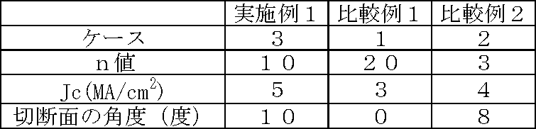
表2に示す結果から、基板を切断していない比較例1の薄膜型超電導素子2に比べて、実施例1及び比較例2の薄膜型超電導素子1、3は、Jc特性が向上していることが確認できる。
また、基板を切断していない比較例1の薄膜型超電導素子2に比べて、超電導層を形成するYBCOが面方向成長の実施例1の薄膜型超電導素子1は、n値特性が低下しているものの、超電導層を形成するYBCOが軸方向成長の比較例2の薄膜型超電導素子3に比べて、その低下の度合いが小さく、超電導層を軸方向成長でなく、面方向成長させることで、n値特性の低下を抑制することができることが確認できた。
また、基板を切断していない比較例1の薄膜型超電導素子2に比べて、超電導層を形成するYBCOが面方向成長の実施例1の薄膜型超電導素子1は、n値特性が低下しているものの、超電導層を形成するYBCOが軸方向成長の比較例2の薄膜型超電導素子3に比べて、その低下の度合いが小さく、超電導層を軸方向成長でなく、面方向成長させることで、n値特性の低下を抑制することができることが確認できた。
薄膜型超電導素子1に用いる基板について、サファイア単結晶からなる基板母材を単結晶のr面方向から切断する角度θを表1のように調整して、実施例2~10に係るサファイア基板を用意した。それ以外は実施例1と同様に薄膜型超電導素子を形成した。
得られた各超電導素子に対して、臨界電流密度(Jc)とn値の測定を行った。
Jcの評価に関して、次のように評価基準を設けた。
・×:3MA/cm3未満
・○:3MA/cm3以上4MA/cm3未満
・◎:4MA/cm3以上
・×:3MA/cm3未満
・○:3MA/cm3以上4MA/cm3未満
・◎:4MA/cm3以上
また、n値に関して、次のように評価基準を設けた。
・△:10未満
・○:10以上20未満
・◎:20以上
・△:10未満
・○:10以上20未満
・◎:20以上

表3から分かるように、実施例1~10に係る薄膜型超電導素子では、比較例1に係る薄膜型超電導素子に比べて、n値特性だけでなくJc特性も良好であった(総合評価が“△”以上の良好)。
また、サファイア単結晶からなる基板母材を単結晶のr面方向から切断する角度θが15度以下であると、Jc特性及びn値特性が共に評価が“○”以上の良好であった(総合評価が“○”以上の良好)。
さらに、サファイア単結晶からなる基板母材を単結晶のr面方向から切断する角度θが2度以上であると、Jc特性が全て“◎”で、他の素子に比べてよりIc特性が良好であった。
さらにまた、サファイア単結晶からなる基板母材を単結晶のr面方向から切断する角度θが2度以上10度以下であると、Jc特性だけでなくn値特性も全て“◎”で、他の素子に比べてJc特性及びn値特性が最も良好であった。
また、サファイア単結晶からなる基板母材を単結晶のr面方向から切断する角度θが15度以下であると、Jc特性及びn値特性が共に評価が“○”以上の良好であった(総合評価が“○”以上の良好)。
さらに、サファイア単結晶からなる基板母材を単結晶のr面方向から切断する角度θが2度以上であると、Jc特性が全て“◎”で、他の素子に比べてよりIc特性が良好であった。
さらにまた、サファイア単結晶からなる基板母材を単結晶のr面方向から切断する角度θが2度以上10度以下であると、Jc特性だけでなくn値特性も全て“◎”で、他の素子に比べてJc特性及びn値特性が最も良好であった。
符号10は、超電導限流器である。
符号12は、密閉容器である。
符号16は、電流導入出部である。
符号24は、素子収容容器である。
符号30は、薄膜型超電導素子(超電導限流素子)である。
符号32は、基板である。
符号32Aは、結晶面である。
符号32Bは、切断面、基板主面である。
符号34Aは、軸、a軸である。
符号34は、中間層である。
符号36Aは、c軸である。
符号36は、超電導層である。
符号40は、電極である。
符号100は、酸化物超電導薄膜である。
符号12は、密閉容器である。
符号16は、電流導入出部である。
符号24は、素子収容容器である。
符号30は、薄膜型超電導素子(超電導限流素子)である。
符号32は、基板である。
符号32Aは、結晶面である。
符号32Bは、切断面、基板主面である。
符号34Aは、軸、a軸である。
符号34は、中間層である。
符号36Aは、c軸である。
符号36は、超電導層である。
符号40は、電極である。
符号100は、酸化物超電導薄膜である。
Claims (9)
- 単結晶構造を有し、前記単結晶構造の結晶面と基板主面が角度を有する基板と、
前記基板主面上に形成され、前記結晶面に対して垂直方向に軸配向した中間層と、
前記中間層上に形成され、前記中間層表面に対して垂直方向にc軸配向した酸化物超電導体を主成分として含有する超電導層と、
を備える酸化物超電導薄膜。 - 前記基板主面と前記単結晶構造の結晶面がなす角度が2度以上15度以下である、
請求項1に記載の酸化物超電導薄膜。 - 前記酸化物超電導体は、組成式REBa2Cu3O7-δ(REは単一の希土類元素又は複数の希土類元素であり、前記δは酸素不定比量である)で表される、
請求項1又は請求項2に記載の酸化物超電導薄膜。 - 前記基板は、サファイア基板であり、
前記結晶面は、r面又はa面であり、
前記中間層は、CeO2又はREMnO3から構成される、
請求項3に記載の酸化物超電導薄膜。 - 前記基板は直方体であり、
前記基板の側面は、前記結晶面と前記基板主面の交線に対し略平行に切断されている、
請求項1~請求項4の何れか1項に記載の酸化物超電導薄膜。 - 内部に液体窒素が充填される密閉容器と、
前記密閉容器の外部から内部へ電流を導入して流出する電流導入出部と、
請求項1~請求項5の何れか1項に記載の酸化物超電導薄膜の超電導層上に電極が形成されて構成され、前記密閉容器内の前記電流導入出部に接続される超電導限流素子と、
を備える超電導限流器。 - 単結晶構造を有した基板を、前記単結晶構造の結晶面から角度を有して切断する工程と、
前記基板の切断面上に、厚さ10nm以上40nm以下の薄い中間層を蒸着して、700℃以上950℃以下の高温でアニールする工程と、
前記中間層上に、c軸方向よりもa軸方向に速い成長速度で超電導層を成膜する工程と、
を有する酸化物超電導薄膜の製造方法。 - 前記超電導層を成膜する工程は、MOD法で成膜する、
請求項7に記載の酸化物超電導薄膜の製造方法。 - 前記超電導層を形成する工程では、a軸方向の成長速度をc軸方向の成長速度の15倍以上25倍以下とする、
請求項7又は請求項8に記載の酸化物超電導薄膜の製造方法。
Priority Applications (4)
| Application Number | Priority Date | Filing Date | Title |
|---|---|---|---|
| JP2013518137A JP5939648B2 (ja) | 2011-05-31 | 2012-05-30 | 酸化物超電導薄膜、超電導限流器及び酸化物超電導薄膜の製造方法 |
| EP12792513.9A EP2716797A4 (en) | 2011-05-31 | 2012-05-30 | SUPERCONDUCTING OXID THIN FILM, SUPERCONDUCTIVE ERROR CURRENT LIMITER, AND METHOD FOR PRODUCING SUPERCONDUCTING OXID THIN FILM |
| SG2013088356A SG195218A1 (en) | 2011-05-31 | 2012-05-30 | Oxide superconductor thin film, superconducting fault current limiter, and method for manufacturing oxide superconductor thin film |
| US14/123,077 US9105794B2 (en) | 2011-05-31 | 2012-05-30 | Oxide superconductor thin film, superconducting fault current limiter, and method for manufacturing oxide superconductor thin film |
Applications Claiming Priority (2)
| Application Number | Priority Date | Filing Date | Title |
|---|---|---|---|
| JP2011-122221 | 2011-05-31 | ||
| JP2011122221 | 2011-05-31 |
Publications (1)
| Publication Number | Publication Date |
|---|---|
| WO2012165504A1 true WO2012165504A1 (ja) | 2012-12-06 |
Family
ID=47259356
Family Applications (1)
| Application Number | Title | Priority Date | Filing Date |
|---|---|---|---|
| PCT/JP2012/063988 Ceased WO2012165504A1 (ja) | 2011-05-31 | 2012-05-30 | 酸化物超電導薄膜、超電導限流器及び酸化物超電導薄膜の製造方法 |
Country Status (5)
| Country | Link |
|---|---|
| US (1) | US9105794B2 (ja) |
| EP (1) | EP2716797A4 (ja) |
| JP (1) | JP5939648B2 (ja) |
| SG (1) | SG195218A1 (ja) |
| WO (1) | WO2012165504A1 (ja) |
Cited By (4)
| Publication number | Priority date | Publication date | Assignee | Title |
|---|---|---|---|---|
| WO2014207946A1 (en) * | 2013-06-28 | 2014-12-31 | National Institute Of Advanced Industrial Science And Technology | Surface layer superconductor and fabrication method of the same |
| WO2015116289A3 (en) * | 2013-11-12 | 2015-10-01 | Varian Semiconductor Equipment Associates, Inc. | Integrated superconductor device and method of fabrication |
| JP2016222467A (ja) * | 2015-05-27 | 2016-12-28 | 国立研究開発法人物質・材料研究機構 | Bi系酸化物超伝導薄膜の製造方法とBi系酸化物超伝導薄膜構造体 |
| US10158061B2 (en) | 2013-11-12 | 2018-12-18 | Varian Semiconductor Equipment Associates, Inc | Integrated superconductor device and method of fabrication |
Citations (7)
| Publication number | Priority date | Publication date | Assignee | Title |
|---|---|---|---|---|
| JPH05279192A (ja) * | 1992-03-27 | 1993-10-26 | Nec Corp | 酸化物超電導薄膜合成方法 |
| JPH0769788A (ja) * | 1993-09-01 | 1995-03-14 | Oki Electric Ind Co Ltd | 酸化物超電導体薄膜の形成方法 |
| JP2003089597A (ja) * | 2001-09-12 | 2003-03-28 | National Institute Of Advanced Industrial & Technology | 基板の表面に形成されたエピタキシャル薄膜及びその製造方法 |
| JP2004303846A (ja) * | 2003-03-31 | 2004-10-28 | Japan Science & Technology Agency | 酸化物超伝導薄膜用バッファ層 |
| JP2005290528A (ja) | 2004-04-05 | 2005-10-20 | National Institute Of Advanced Industrial & Technology | サファイア基板上高臨界面電流超電導酸化物薄膜及びその作製方法 |
| JP2006273699A (ja) * | 2005-03-30 | 2006-10-12 | National Institute Of Advanced Industrial & Technology | 高品質Bi系酸化物超電導薄膜の作製法 |
| JP2011122221A (ja) | 2009-12-11 | 2011-06-23 | Nisshin Steel Co Ltd | めっき鋼帯製造装置及びめっき鋼帯製造方法 |
Family Cites Families (7)
| Publication number | Priority date | Publication date | Assignee | Title |
|---|---|---|---|---|
| US5162294A (en) * | 1991-02-28 | 1992-11-10 | Westinghouse Electric Corp. | Buffer layer for copper oxide based superconductor growth on sapphire |
| US5262394A (en) * | 1991-12-27 | 1993-11-16 | The United States Of America As Represented By The United States Department Of Energy | Superconductive articles including cerium oxide layer |
| JP3392653B2 (ja) * | 1996-09-02 | 2003-03-31 | 財団法人国際超電導産業技術研究センター | 酸化物超電導体ジョセフソン接合素子及びその製造方法 |
| US8088713B2 (en) * | 2004-06-24 | 2012-01-03 | National Institute Of Advanced Industrial Science And Technology | Superconducting fault-current limiting element and the process for producing the same |
| JP5219109B2 (ja) * | 2005-08-10 | 2013-06-26 | 独立行政法人産業技術総合研究所 | 超電導材料の製造方法 |
| DE602008002152D1 (de) * | 2008-06-27 | 2010-09-23 | Nexans | Strombegrenzungsvorrichtung |
| JP5472682B2 (ja) * | 2009-05-01 | 2014-04-16 | 独立行政法人産業技術総合研究所 | 超電導限流素子 |
-
2012
- 2012-05-30 WO PCT/JP2012/063988 patent/WO2012165504A1/ja not_active Ceased
- 2012-05-30 EP EP12792513.9A patent/EP2716797A4/en not_active Withdrawn
- 2012-05-30 US US14/123,077 patent/US9105794B2/en active Active
- 2012-05-30 SG SG2013088356A patent/SG195218A1/en unknown
- 2012-05-30 JP JP2013518137A patent/JP5939648B2/ja not_active Expired - Fee Related
Patent Citations (7)
| Publication number | Priority date | Publication date | Assignee | Title |
|---|---|---|---|---|
| JPH05279192A (ja) * | 1992-03-27 | 1993-10-26 | Nec Corp | 酸化物超電導薄膜合成方法 |
| JPH0769788A (ja) * | 1993-09-01 | 1995-03-14 | Oki Electric Ind Co Ltd | 酸化物超電導体薄膜の形成方法 |
| JP2003089597A (ja) * | 2001-09-12 | 2003-03-28 | National Institute Of Advanced Industrial & Technology | 基板の表面に形成されたエピタキシャル薄膜及びその製造方法 |
| JP2004303846A (ja) * | 2003-03-31 | 2004-10-28 | Japan Science & Technology Agency | 酸化物超伝導薄膜用バッファ層 |
| JP2005290528A (ja) | 2004-04-05 | 2005-10-20 | National Institute Of Advanced Industrial & Technology | サファイア基板上高臨界面電流超電導酸化物薄膜及びその作製方法 |
| JP2006273699A (ja) * | 2005-03-30 | 2006-10-12 | National Institute Of Advanced Industrial & Technology | 高品質Bi系酸化物超電導薄膜の作製法 |
| JP2011122221A (ja) | 2009-12-11 | 2011-06-23 | Nisshin Steel Co Ltd | めっき鋼帯製造装置及びめっき鋼帯製造方法 |
Non-Patent Citations (2)
| Title |
|---|
| M SOHMA ET AL.: "Structural aspect of high-JcMOD-YBCO films prepared on large area Ce02-buffered YSZsubstrates", J. PHYS.: CONF., vol. 43, no. 1, 2006, pages 349 - 352, XP020110251 * |
| See also references of EP2716797A4 |
Cited By (8)
| Publication number | Priority date | Publication date | Assignee | Title |
|---|---|---|---|---|
| WO2014207946A1 (en) * | 2013-06-28 | 2014-12-31 | National Institute Of Advanced Industrial Science And Technology | Surface layer superconductor and fabrication method of the same |
| JP2016531061A (ja) * | 2013-06-28 | 2016-10-06 | 国立研究開発法人産業技術総合研究所 | 表層超電導体の製造方法および表層超電導体 |
| WO2015116289A3 (en) * | 2013-11-12 | 2015-10-01 | Varian Semiconductor Equipment Associates, Inc. | Integrated superconductor device and method of fabrication |
| CN105849888A (zh) * | 2013-11-12 | 2016-08-10 | 瓦里安半导体设备公司 | 积体超导体装置及其制造方法 |
| US9947441B2 (en) | 2013-11-12 | 2018-04-17 | Varian Semiconductor Equipment Associates, Inc. | Integrated superconductor device and method of fabrication |
| US10158061B2 (en) | 2013-11-12 | 2018-12-18 | Varian Semiconductor Equipment Associates, Inc | Integrated superconductor device and method of fabrication |
| US10290399B2 (en) | 2013-11-12 | 2019-05-14 | Varian Semiconductor Equipment Associates, Inc. | Integrated superconductor device and method of fabrication |
| JP2016222467A (ja) * | 2015-05-27 | 2016-12-28 | 国立研究開発法人物質・材料研究機構 | Bi系酸化物超伝導薄膜の製造方法とBi系酸化物超伝導薄膜構造体 |
Also Published As
| Publication number | Publication date |
|---|---|
| EP2716797A4 (en) | 2014-10-29 |
| JP5939648B2 (ja) | 2016-06-22 |
| US20140080714A1 (en) | 2014-03-20 |
| US9105794B2 (en) | 2015-08-11 |
| JPWO2012165504A1 (ja) | 2015-02-23 |
| EP2716797A1 (en) | 2014-04-09 |
| SG195218A1 (en) | 2013-12-30 |
Similar Documents
| Publication | Publication Date | Title |
|---|---|---|
| JP4713012B2 (ja) | テープ状酸化物超電導体 | |
| US6436317B1 (en) | Oxide bronze compositions and textured articles manufactured in accordance therewith | |
| CN104737243B (zh) | 氧化物超导薄膜 | |
| US11488746B2 (en) | Superconductor with improved flux pinning at low temperatures | |
| JP5244337B2 (ja) | テープ状酸化物超電導体 | |
| CN102870244B (zh) | 单涂层的厚氧化物膜 | |
| JP5513154B2 (ja) | 酸化物超電導線材及び酸化物超電導線材の製造方法 | |
| JP5939648B2 (ja) | 酸化物超電導薄膜、超電導限流器及び酸化物超電導薄膜の製造方法 | |
| JP6090794B2 (ja) | 酸化物超電導薄膜および超電導限流器 | |
| US20130137580A1 (en) | Substrate for superconducting thin film, superconducting thin film, and method of producing superconducting thin film | |
| US9136046B2 (en) | Superconducting wire rod and method for manufacturing superconducting wire rod | |
| EP2940698B1 (en) | Re-123 superconducting wire and manufacturing method therefor | |
| JP2012022882A (ja) | 酸化物超電導導体用基材及びその製造方法と酸化物超電導導体及びその製造方法 | |
| EP2343745A1 (en) | Coated conductor with improved grain orientation | |
| CN103052997B (zh) | 超导线材用基材、超导线材和超导线材的制造方法 | |
| JP2011249162A (ja) | 超電導線材の製造方法 | |
| EP2607317A1 (en) | Oxide superconducting thin film | |
| JP2016143516A (ja) | 酸化物超電導線材及びその製造方法 | |
| JP2014003270A (ja) | 酸化物超電導薄膜 | |
| JP2013008958A (ja) | 酸化物超電導薄膜 |
Legal Events
| Date | Code | Title | Description |
|---|---|---|---|
| 121 | Ep: the epo has been informed by wipo that ep was designated in this application |
Ref document number: 12792513 Country of ref document: EP Kind code of ref document: A1 |
|
| ENP | Entry into the national phase |
Ref document number: 2013518137 Country of ref document: JP Kind code of ref document: A |
|
| WWE | Wipo information: entry into national phase |
Ref document number: 14123077 Country of ref document: US |
|
| NENP | Non-entry into the national phase |
Ref country code: DE |