WO2012165617A1 - Dispositif d'affichage à cristaux liquides - Google Patents
Dispositif d'affichage à cristaux liquides Download PDFInfo
- Publication number
- WO2012165617A1 WO2012165617A1 PCT/JP2012/064277 JP2012064277W WO2012165617A1 WO 2012165617 A1 WO2012165617 A1 WO 2012165617A1 JP 2012064277 W JP2012064277 W JP 2012064277W WO 2012165617 A1 WO2012165617 A1 WO 2012165617A1
- Authority
- WO
- WIPO (PCT)
- Prior art keywords
- layer electrode
- liquid crystal
- lower layer
- electrode
- electrode fingers
- Prior art date
- Legal status (The legal status is an assumption and is not a legal conclusion. Google has not performed a legal analysis and makes no representation as to the accuracy of the status listed.)
- Ceased
Links
Images


























Classifications
-
- G—PHYSICS
- G02—OPTICS
- G02F—OPTICAL DEVICES OR ARRANGEMENTS FOR THE CONTROL OF LIGHT BY MODIFICATION OF THE OPTICAL PROPERTIES OF THE MEDIA OF THE ELEMENTS INVOLVED THEREIN; NON-LINEAR OPTICS; FREQUENCY-CHANGING OF LIGHT; OPTICAL LOGIC ELEMENTS; OPTICAL ANALOGUE/DIGITAL CONVERTERS
- G02F1/00—Devices or arrangements for the control of the intensity, colour, phase, polarisation or direction of light arriving from an independent light source, e.g. switching, gating or modulating; Non-linear optics
- G02F1/01—Devices or arrangements for the control of the intensity, colour, phase, polarisation or direction of light arriving from an independent light source, e.g. switching, gating or modulating; Non-linear optics for the control of the intensity, phase, polarisation or colour
- G02F1/13—Devices or arrangements for the control of the intensity, colour, phase, polarisation or direction of light arriving from an independent light source, e.g. switching, gating or modulating; Non-linear optics for the control of the intensity, phase, polarisation or colour based on liquid crystals, e.g. single liquid crystal display cells
- G02F1/133—Constructional arrangements; Operation of liquid crystal cells; Circuit arrangements
- G02F1/1333—Constructional arrangements; Manufacturing methods
- G02F1/1343—Electrodes
- G02F1/134309—Electrodes characterised by their geometrical arrangement
-
- G—PHYSICS
- G02—OPTICS
- G02F—OPTICAL DEVICES OR ARRANGEMENTS FOR THE CONTROL OF LIGHT BY MODIFICATION OF THE OPTICAL PROPERTIES OF THE MEDIA OF THE ELEMENTS INVOLVED THEREIN; NON-LINEAR OPTICS; FREQUENCY-CHANGING OF LIGHT; OPTICAL LOGIC ELEMENTS; OPTICAL ANALOGUE/DIGITAL CONVERTERS
- G02F1/00—Devices or arrangements for the control of the intensity, colour, phase, polarisation or direction of light arriving from an independent light source, e.g. switching, gating or modulating; Non-linear optics
- G02F1/01—Devices or arrangements for the control of the intensity, colour, phase, polarisation or direction of light arriving from an independent light source, e.g. switching, gating or modulating; Non-linear optics for the control of the intensity, phase, polarisation or colour
- G02F1/13—Devices or arrangements for the control of the intensity, colour, phase, polarisation or direction of light arriving from an independent light source, e.g. switching, gating or modulating; Non-linear optics for the control of the intensity, phase, polarisation or colour based on liquid crystals, e.g. single liquid crystal display cells
- G02F1/133—Constructional arrangements; Operation of liquid crystal cells; Circuit arrangements
- G02F1/1333—Constructional arrangements; Manufacturing methods
- G02F1/1343—Electrodes
- G02F1/134309—Electrodes characterised by their geometrical arrangement
- G02F1/134363—Electrodes characterised by their geometrical arrangement for applying an electric field parallel to the substrate, i.e. in-plane switching [IPS]
-
- G—PHYSICS
- G02—OPTICS
- G02F—OPTICAL DEVICES OR ARRANGEMENTS FOR THE CONTROL OF LIGHT BY MODIFICATION OF THE OPTICAL PROPERTIES OF THE MEDIA OF THE ELEMENTS INVOLVED THEREIN; NON-LINEAR OPTICS; FREQUENCY-CHANGING OF LIGHT; OPTICAL LOGIC ELEMENTS; OPTICAL ANALOGUE/DIGITAL CONVERTERS
- G02F1/00—Devices or arrangements for the control of the intensity, colour, phase, polarisation or direction of light arriving from an independent light source, e.g. switching, gating or modulating; Non-linear optics
- G02F1/01—Devices or arrangements for the control of the intensity, colour, phase, polarisation or direction of light arriving from an independent light source, e.g. switching, gating or modulating; Non-linear optics for the control of the intensity, phase, polarisation or colour
- G02F1/13—Devices or arrangements for the control of the intensity, colour, phase, polarisation or direction of light arriving from an independent light source, e.g. switching, gating or modulating; Non-linear optics for the control of the intensity, phase, polarisation or colour based on liquid crystals, e.g. single liquid crystal display cells
- G02F1/133—Constructional arrangements; Operation of liquid crystal cells; Circuit arrangements
- G02F1/1333—Constructional arrangements; Manufacturing methods
- G02F1/1343—Electrodes
- G02F1/134309—Electrodes characterised by their geometrical arrangement
- G02F1/134318—Electrodes characterised by their geometrical arrangement having a patterned common electrode
-
- G—PHYSICS
- G02—OPTICS
- G02F—OPTICAL DEVICES OR ARRANGEMENTS FOR THE CONTROL OF LIGHT BY MODIFICATION OF THE OPTICAL PROPERTIES OF THE MEDIA OF THE ELEMENTS INVOLVED THEREIN; NON-LINEAR OPTICS; FREQUENCY-CHANGING OF LIGHT; OPTICAL LOGIC ELEMENTS; OPTICAL ANALOGUE/DIGITAL CONVERTERS
- G02F1/00—Devices or arrangements for the control of the intensity, colour, phase, polarisation or direction of light arriving from an independent light source, e.g. switching, gating or modulating; Non-linear optics
- G02F1/01—Devices or arrangements for the control of the intensity, colour, phase, polarisation or direction of light arriving from an independent light source, e.g. switching, gating or modulating; Non-linear optics for the control of the intensity, phase, polarisation or colour
- G02F1/13—Devices or arrangements for the control of the intensity, colour, phase, polarisation or direction of light arriving from an independent light source, e.g. switching, gating or modulating; Non-linear optics for the control of the intensity, phase, polarisation or colour based on liquid crystals, e.g. single liquid crystal display cells
- G02F1/133—Constructional arrangements; Operation of liquid crystal cells; Circuit arrangements
- G02F1/1333—Constructional arrangements; Manufacturing methods
- G02F1/1343—Electrodes
- G02F1/134309—Electrodes characterised by their geometrical arrangement
- G02F1/134372—Electrodes characterised by their geometrical arrangement for fringe field switching [FFS] where the common electrode is not patterned
Definitions
- the present invention relates to a liquid crystal display device.
- This application claims priority on June 3, 2011 based on Japanese Patent Application No. 2011-125186 for which it applied to Japan, and uses the content here.
- a horizontal electric field method is conventionally known as a method for applying an electric field to a liquid crystal layer.
- a horizontal electric field type liquid crystal display device a common electrode and a pixel electrode are provided on one of a pair of substrates sandwiching a liquid crystal layer, and substantially in a horizontal direction (a direction substantially parallel to the substrate) with respect to the liquid crystal layer. The electric field of is applied.
- the horizontal electric field type liquid crystal display device includes an IPS (In-Plane Switching) type liquid crystal display device and an FFS (Fringe Field Switching) type liquid crystal display device depending on a difference in electrode configuration.
- An FFS mode liquid crystal display device generally includes a lower layer electrode formed in substantially the entire region of a pixel, and an upper layer electrode having a plurality of slits arranged on the lower layer electrode with an insulating film interposed therebetween.
- a liquid crystal display device having a shape in which a common electrode (lower layer electrode) and a pixel electrode (upper layer electrode) are bent in a pixel and a data line is also bent in parallel with these electrodes has been proposed (for example, Patent Document 2) below.
- the common electrode and the pixel electrode are bent so that the inside of the pixel is multi-domain and the viewing angle is improved.
- a liquid crystal display device in which a plurality of openings are provided in the lower electrode in addition to the upper electrode has been proposed (for example, Patent Document 3 below).
- an opening is formed in a region of the lower layer electrode that overlaps with the upper layer electrode. Therefore, the area of the overlapping portion between the upper layer electrode and the lower layer electrode is reduced. As a result, the load capacity composed of the upper layer electrode, the lower layer electrode, and the insulating film sandwiched between these electrodes can be reduced. As a result, the writing speed of information on the liquid crystal can be increased, and an image with high display quality can be obtained.
- An object of an aspect of the present invention is to provide a liquid crystal display device having an electrode structure that can reduce load capacity. It is another object of the present invention to provide a liquid crystal display device that can suppress variation in characteristics as much as possible even when alignment between the upper electrode and the lower electrode occurs.
- a liquid crystal display device includes: a pair of substrates disposed opposite to each other; a liquid crystal layer sandwiched between the pair of substrates; and one of the pair of substrates and the liquid crystal layer.
- a plurality of lower layers each including a lower layer electrode provided therebetween, an insulating film covering the lower layer electrode, and an upper layer electrode provided on the insulating film, wherein the lower layer electrode is disposed at a predetermined interval
- the upper electrode has a plurality of upper electrode fingers arranged at a predetermined interval, and the lower electrode finger and the upper electrode finger are arranged in a normal direction of the one substrate. When viewed, they intersect at a predetermined angle greater than 0 ° and less than 90 °.
- the one substrate has a plurality of pixel regions arranged in a matrix, and the plurality of lower layer electrode fingers are arranged in an arrangement direction of the plurality of pixel regions.
- the plurality of upper layer electrode fingers may extend in parallel and be inclined with respect to an arrangement direction of the plurality of pixel regions.
- the line width of the first portion of the plurality of lower layer electrode fingers in the vicinity of at least one of the intersections of the plurality of lower layer electrode fingers and the plurality of upper layer electrode fingers is It may be wider than the line width of the second portion adjacent to the first portion and other than the vicinity of at least one of the intersecting portions.
- an edge of a portion adjacent to the second portion in the first portion extends in an extending direction of the plurality of lower layer electrode fingers.
- An angle greater than 0 ° and less than 90 ° may be formed.
- an edge of a portion adjacent to the second portion of the first portion is relative to an edge of the plurality of upper layer electrode fingers. It may be approximately parallel.
- a part of the plurality of lower layer electrode fingers may be missing at at least one of intersections of the plurality of lower layer electrode fingers and the plurality of upper layer electrode fingers.
- the line width of the plurality of upper electrode fingers is L1
- the interval between the adjacent upper electrode fingers is S1
- the line width of the plurality of lower electrode fingers is L2
- the interval between the plurality of lower layer electrode fingers is S2
- L1 + S1> L2 + S2 This condition may be satisfied.
- the line width of the plurality of upper electrode fingers is L1
- the interval between the adjacent upper electrode fingers is S1
- the line width of the plurality of lower electrode fingers is L2
- L1 + S1 L2 + S2 and L1 ⁇ L2
- the load capacity can be reduced and the display characteristics can be improved. Further, even when the alignment deviation between the upper layer electrode and the lower layer electrode occurs, the characteristic variation can be suppressed as much as possible.
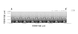
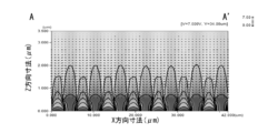
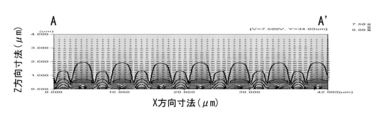
- FIG. 23 is a diagram showing a distribution of equipotential lines and directors of liquid crystal molecules at the position of the A-A ′ line in FIG. 22.
- FIG. 23 is a diagram showing distribution of equipotential lines and directors of liquid crystal molecules at the position of the B-B ′ line in FIG. 22.
- FIG. 26 is a diagram showing the distribution of equipotential lines and directors of liquid crystal molecules at the position of the A-A ′ line in FIG. 25. It is a figure which shows the electrode pattern used for the simulation of 3rd Example, and is a top view of a lower layer electrode. It is a figure which shows the electrode pattern used for the simulation of 3rd Example, and is a top view of an upper layer electrode.
- FIG. 33 is a diagram showing distribution of equipotential lines and directors of liquid crystal molecules at the position of the A-A ′ line in FIG.
- FIG. 38 is a diagram showing equipotential lines and the distribution of directors of liquid crystal molecules at the position of the A-A ′ line in FIG. 37. It is a graph which shows the relationship between the applied voltage and capacity
- FIG. 43 is a diagram showing distribution of equipotential lines and directors of liquid crystal molecules at the position of the A-A ′ line in FIG. 42. It is a graph which shows the relationship between the applied voltage and the transmittance
- FIG. 47 is a diagram showing a distribution of equipotential lines and directors of liquid crystal molecules at the position of the A-A ′ line in FIG. 46. It is a graph which shows the relationship between the applied voltage and a capacity
- the liquid crystal display device includes a pair of electrodes on one of a pair of substrates sandwiching a liquid crystal layer, and a liquid crystal of a lateral electric field type that drives the liquid crystal with an electric field applied between the pair of electrodes. It is a display device.
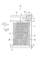
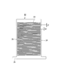
- FIG. 1 is an exploded perspective view showing a schematic configuration of the liquid crystal display device of the present embodiment.
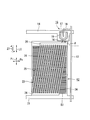
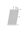
- FIG. 2 is a plan view showing one pixel of the liquid crystal display device of the present embodiment.
- the scale of the size may be varied depending on the component.
- the liquid crystal display device 1 of the present embodiment includes a backlight 2, a polarizing plate 3, a liquid crystal cell 4, and a polarizing plate 5 from the back as viewed from the observer. . Therefore, the liquid crystal display device 1 of the present embodiment is a transmissive liquid crystal display device, and performs display by controlling the transmittance of light emitted from the backlight 2 by the liquid crystal cell 4.
- the liquid crystal cell 4 includes a thin film transistor (Thin Film Transistor, hereinafter abbreviated as TFT) array substrate 6 and a counter substrate 7, and a liquid crystal layer 8 is disposed between the TFT array substrate 6 and the counter substrate 7. It is pinched. Generally, a positive type liquid crystal material is used for the liquid crystal layer 8, but a negative type liquid crystal material may be used.
- TFT array substrate 6 has a plurality of pixel regions 10 arranged in a matrix on a substrate 9, and a display region (screen) is configured by these pixel regions 10.
- the counter substrate 7 includes a color filter 12 on a substrate 11.
- the display region has a plurality of source bus lines arranged in parallel to each other and a plurality of gate bus lines arranged in parallel to each other.
- the plurality of source bus lines and the plurality of gate bus lines are arranged orthogonally.
- the display area is partitioned in a lattice pattern by a plurality of source bus lines and a plurality of gate bus lines, and the partitioned rectangular area becomes the pixel area 10.
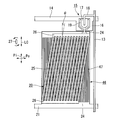
- a TFT 15 is provided in the vicinity of the intersection where the source bus line 13 and the gate bus line 14 intersect.
- the TFT 15 of this embodiment includes a gate electrode 16 formed integrally with the gate bus line 14, a semiconductor layer 17 disposed on the gate electrode 16, a source electrode 18 formed integrally with the source bus line 13, And a drain electrode 19.
- the drain electrode 19 has a U-shape and is arranged so as to surround the source electrode 18.
- the drain electrode 19 is electrically connected to an upper layer electrode 20 described later.
- a common bus line 21 is disposed along a side opposite to the side where the gate bus line 14 is disposed.
- the common bus line 21 is electrically connected to a lower layer electrode 22 described later.
- the lower layer electrode 22 and the upper layer electrode 20 are drawn so as to overlap each other, but an insulating film is formed so as to cover the lower layer electrode 22, and the upper layer electrode 20 is formed on the insulating film.
- a common potential for example, 0 V
- a pixel potential for example, + several V
- the application direction of the potential is not limited to the above, and a configuration in which a pixel potential is applied to the lower layer electrode 22 and a common potential is applied to the upper layer electrode 20 may be employed. It may be considered equivalent regardless of which potential is applied to which electrode. Therefore, contrary to the above configuration, the lower electrode 22 may be connected to the drain electrode 19 of the TFT 15 and the upper electrode 20 may be connected to the common bus line 21.
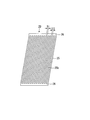
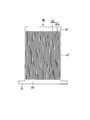
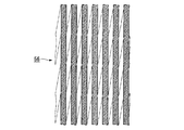
- the lower layer electrode 22 has a plurality of lower layer electrode fingers 23 arranged in parallel with each other at a predetermined interval.
- the plurality of lower layer electrode fingers 23 are integrally connected and electrically connected by a connecting portion 24 provided on the upper side and the lower side in FIG. 3A.
- the plurality of lower layer electrode fingers 23 extend in parallel with the source bus line 13. That is, the plurality of lower layer electrode fingers 23 are arranged so as to extend in parallel with the arrangement direction of the plurality of pixel regions 10.
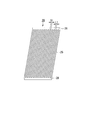
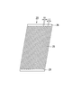
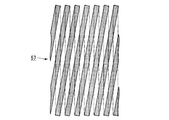
- the upper layer electrode 20 has a plurality of upper layer electrode fingers 25 arranged in parallel with each other at a predetermined interval.
- the plurality of upper layer electrode fingers 25 are integrally connected and electrically connected by a connecting portion 26 provided on the upper side and the lower side in FIG. 3B.
- the upper electrode finger 25 is disposed so as to intersect with the lower electrode finger 23 at a predetermined angle larger than 0 ° and smaller than 90 °.
- the upper electrode finger 25 intersects the lower electrode finger 23 at an angle of 10 °. That is, as shown in FIG. 2, the crossing angle ⁇ between the upper electrode finger 25 and the lower electrode finger 23 is 10 °. Therefore, the upper electrode finger 25 extends in a direction that forms an angle of 10 ° with the source bus line 13.
- the lower layer electrode 22 and the upper layer electrode 20 are both composed of a transparent conductive film such as indium tin oxide (Indium Tin Oxide, ITO), indium zinc oxide (IZO (registered trademark, Idemitsu Kosan Co., Ltd.)), or the like.
- the insulating film interposed between the lower layer electrode 22 and the upper layer electrode 20 is made of, for example, a silicon nitride film.
- the line width of the upper electrode finger 25 is L1
- the interval between the adjacent upper electrode fingers 25 is S1
- the line width of the lower electrode finger 23 is L2
- the interval between the adjacent lower electrode fingers 23 is S2.
- L1 3 ⁇ m
- S1 3 ⁇ m
- L2 3 ⁇ m
- S2 3 ⁇ m
- L2 / S2 3/3 ⁇ m.
- the film thickness of the transparent conductive film constituting the lower layer electrode 22 is 80 nm
- the film thickness of the transparent conductive film constituting the upper layer electrode 20 is 80 nm
- the film thickness of the insulating film is 500 nm.
- An alignment film subjected to an alignment process such as rubbing is provided on the surface of the TFT array substrate 6 and the counter substrate 7 on the liquid crystal layer 8 side.
- the alignment direction of the liquid crystal molecules 27 constituting the liquid crystal layer 8 when the electric field is not applied is regulated by the alignment film.
- the alignment direction when no electric field is applied to the liquid crystal molecules 27 is referred to as an initial alignment direction.
- the alignment film of the TFT array substrate 6 and the alignment film of the counter substrate 7 are subjected to the alignment process in the same direction. As shown by the arrow LC in FIG. 2, the alignment process direction, that is, the initial alignment direction of the liquid crystal molecules 27 is restricted to a direction parallel to the extending direction of the lower layer electrode finger 23.
- the initial alignment direction of the liquid crystal molecules 27 is restricted to a direction that forms an angle of 10 ° with the extending direction of the upper electrode fingers 25. Therefore, when a positive type liquid crystal is used, when a voltage is applied between the lower layer electrode 22 and the upper layer electrode 20, the liquid crystal molecules 27 are separated from the substrate surface according to the direction of the transverse electric field generated between the electrodes 22 and 20. Rotates counterclockwise in a substantially parallel plane.
- the two polarizing plates 3 and 5 arranged on the outside of the liquid crystal cell 4 are arranged in crossed Nicols so that the transmission axis is parallel and perpendicular to the initial alignment direction of the liquid crystal molecules 27.
- the polarizing plate 3 on the light incident side is disposed so that the transmission axis is in a direction parallel to the extending direction of the lower layer electrode finger 23 (direction of the arrow Pi).
- the polarizing plate 5 on the light emission side is arranged so that the transmission axis is in a direction perpendicular to the extending direction of the lower layer electrode finger 23 (the direction of the arrow Po).
- the liquid crystal display device 1 of this embodiment functions as a so-called normally black mode liquid crystal display device in which black display is performed when no electric field is applied and white display is applied when an electric field is applied.
- the lower layer electrode is disposed over substantially the entire surface of the pixel region, and overlaps the lower layer electrode in almost all regions where the upper layer electrode exists.
- the line width and spacing of the upper layer electrode is 1: 1, both electrodes overlap in a half of all electrode formation regions, and the load capacity becomes very large. It was.
- the lower layer electrode 22 in addition to the upper layer electrode 20, the lower layer electrode 22 also has a shape having a plurality of lower layer electrode fingers 23, and the upper layer electrode fingers 25 and the lower layer electrode fingers 23 are 10 It is arranged to cross at an angle of °. Thereby, only the intersection where the upper electrode finger 25 and the lower electrode finger 23 intersect becomes an area where the upper electrode 20 and the lower electrode 22 overlap. Therefore, in the liquid crystal display device 1 of this embodiment, the load capacity can be greatly reduced as compared with the conventional FFS type liquid crystal display device. As a result, power consumption required for driving can be reduced, which is suitable for mobile use. In television applications, it is possible to increase the screen size, improve the response, and perform the double speed drive or the quadruple speed drive for stereoscopic display without any trouble.
- 4A and 4B are enlarged views of a part of the lower layer electrode finger 23 and the upper layer electrode finger 25.
- the upper electrode finger 25 is displaced by 1.5 ⁇ m in the right direction and 3.0 ⁇ m in the lower direction.
- 4A shows a normal state and FIG. 4B shows a shifted state.
- the parallelogram area indicated by reference numeral 28 is an intersection of the lower electrode finger 23 and the upper electrode finger 25. The total area of all the intersections 28 occupies 1/4 of the total area of the electrode formation region. Accordingly, in view of area calculation, in this embodiment, the load capacity can be reduced by 50% compared to the conventional FFS type liquid crystal display device.
- the shape of the electrode formation region is generally rectangular, the effect of misalignment actually occurs on the four sides (upper and lower edges of the pixel).
- the influence of the peripheral edge on the entire pixel is negligible and can be almost ignored.
- the area of the intersecting portion 28 may change, but it is considered that a large misalignment occurs in the rotation direction in the manufacturing process. Hateful. Further, even if a slight misalignment in the rotational direction occurs, this effect is slight and can be almost ignored.
- a plurality of lower layer electrode fingers 23 are arranged in parallel to the extending direction of the source bus lines 13 (pixel arrangement direction), and a plurality of upper layer electrode fingers 25 are arranged with respect to the plurality of lower layer electrode fingers 23. And tilted 10 °. Therefore, the direction of the alignment process of the TFT array substrate 6 and the counter substrate 7 is set to the extending direction of the source bus lines 13 (pixel arrangement direction), that is, the direction parallel or perpendicular to the edges of the TFT array substrate 6 and the counter substrate 7 It ’s fine. Therefore, the arrangement of the electrodes is preferable in that an alignment process such as rubbing can be easily performed. Also, the polarizing plates 3 and 5 can be arranged easily because the direction of the transmission axis should be aligned with the direction parallel to or perpendicular to the edges of the TFT array substrate 6 and the counter substrate 7. preferable.
- the plurality of lower layer electrode fingers 23 are inclined by 10 ° with respect to the extending direction of the source bus lines 13 (pixel arrangement direction), contrary to the above configuration.
- the plurality of upper layer electrode fingers 25 may be arranged in parallel to the extending direction of the source bus lines 13 (pixel arrangement direction).
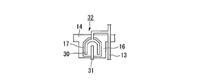
- the TFT 15 having a configuration in which the U-shaped drain electrode 19 surrounds the linear source electrode 18 is used.
- the source electrode 30 connected to the source bus line 13 is formed in a U-shape
- the TFT 32 having a configuration in which the source electrode 30 surrounds the straight drain electrode 31 is formed. It may be used.
- the drain electrode is also formed as in the present embodiment rather than having a U-shaped source electrode. It is desirable to make it U-shaped.
- the reason is as follows.
- the W / L (gate width / gate length) of the TFT increases, so that the charge writing ability to the pixel is increased. Can do.
- the drain electrode and the source electrode are U-shaped, the area of the overlapping portion between these electrodes and the gate electrode increases.
- the gate-drain parasitic capacitance Cgd increases, and when the source electrode is U-shaped, the gate-source parasitic capacitance Cgs increases.
- an increase in the parasitic capacitance Cgd between the gate and the drain leads to an increase in the feedthrough voltage, which affects the reliability of the liquid crystal display device including the burn-in.
- an increase in the parasitic capacitance Cgs between the gate and the source leads to an increase in the load on the bus line, which causes a signal delay and may cause display unevenness due to a difference in distance from the driver.
- the FFS liquid crystal display device tends to have a larger sum (Clc + Cs) of the liquid crystal capacitance Clc and the auxiliary capacitance Cs than other types of liquid crystal display devices. Therefore, even if the gate-drain parasitic capacitance Cgd is somewhat increased by making the drain electrode U-shaped, there is little influence on the overall capacitance (Clc + Cs + Cgd), and the reliability of the liquid crystal display device is greatly affected. Does not affect. On the other hand, when the gate-source parasitic capacitance Cgs is reduced by making the drain electrode U-shaped and the source electrode linear, the load on the source bus line is reduced and signal delay can be reduced. As a result, sufficient charge can be written in each pixel electrode in a short writing time, and display unevenness can be reduced.
- FIG. 6 is a plan view showing one pixel of the liquid crystal display device of this embodiment.
- FIG. 7A is a plan view showing the lower layer electrode.
- FIG. 7B is a plan view showing the upper layer electrode.
- FIG. 8 is an enlarged view of the intersection between the lower layer electrode and the upper layer electrode. 6 to 8, the same components as those in FIGS. 1 to 3B of the first embodiment are denoted by the same reference numerals, and description thereof is omitted.
- the line width of the lower layer electrode finger 36 is other than the vicinity of the intersection portion 28 in the vicinity of the intersection portion 28 between the lower layer electrode finger 36 and the upper layer electrode finger 25. It is wider than the line width of the part.
- the line width of the first portion of the lower layer electrode finger 36 in the vicinity of at least one of the intersecting portions 28 of the plurality of lower layer electrode fingers 36 and the plurality of upper layer electrode fingers 25 is adjacent to the first portion and intersects.
- the line width of the second portion other than the vicinity of at least one of the portions 28 is wider.
- a portion where the line width of the lower electrode finger 36 is increased with respect to a portion where the line width is constant is hereinafter referred to as a widened portion 37.
- the load capacity can be reduced as compared with the conventional FFS type liquid crystal display device, the power consumption required for driving can be reduced, and high speed driving can be performed without any trouble. Can be obtained.
- the lower electrode finger 23 is exposed to the side of the upper electrode finger 25 at the intersection 28 between the lower electrode finger 23 and the upper electrode finger 25 when viewed from the normal direction of the TFT array substrate 6. Absent. Therefore, when an electric field is applied, a lateral electric field is not generated in the vicinity of the intersection 28 between the lower electrode finger 23 and the upper electrode finger 25, and the liquid crystal molecules are not aligned in a desired direction, so that the transmittance may be lowered.
- the widened portion 37 is provided in the vicinity of the intersecting portion 28 between the lower electrode finger 36 and the upper electrode finger 25, the widened portion is formed on the side of the upper electrode finger 25 as shown in FIG. 37 is exposed.
- the widened portion 37 of the lower electrode finger 36 is located in a region where the upper electrode finger 25 does not exist, the area of the overlapping portion between the lower electrode finger 36 and the upper electrode finger 25 hardly increases. Therefore, the increase in load capacity is minimized.
- FIG. 9 is a plan view showing one pixel of the liquid crystal display device of this embodiment.
- FIG. 10A is a plan view showing a lower layer electrode.
- FIG. 10B is a plan view showing the upper layer electrode.
- FIG. 11 is an enlarged view of the intersection between the lower layer electrode and the upper layer electrode. 9 to 11, the same reference numerals are given to the same components as those in FIGS. 1 to 3B of the first embodiment, and the description thereof will be omitted.
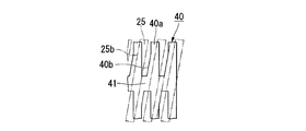
- the width of the lower layer electrode finger 40 is increased from the constant line width portion 40a in the vicinity of the intersection 28 between the lower layer electrode finger 40 and the upper layer electrode finger 25.
- the edge 40b of the lower layer electrode finger 40 reaching the portion 41 extends obliquely at an angle other than 90 ° with respect to the edge of the lower layer electrode finger 40 in the constant line width portion 40a.
- the edge 40b of the lower layer electrode finger 40 extending from the constant line width portion 40a of the lower layer electrode finger 40 to the widened portion 41 has an angle of 10 ° with respect to the edge of the lower layer electrode finger 40 in the constant line width portion 40a. There is no.
- the edge of the widened portion 41 adjacent to the constant line width portion 40a forms an angle larger than 0 ° and smaller than 90 ° with respect to the extending direction of the lower layer electrode finger 39. Since the edge 40b of the lower layer electrode finger 40 extending from the constant line width portion 40a of the lower layer electrode finger 40 to the widened portion 41 is designed as described above, as shown in FIG. The edge 40b of the lower layer electrode finger 40 extending from 40a to the widened portion 41 is substantially parallel to the edge 25b of the upper layer electrode finger 25.
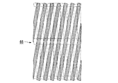
- the corners of the elongated rectangular slits between adjacent lower layer electrode fingers 36 in the lower layer electrode 35 of the second embodiment shown in FIG. 7A are tapered. It can also be said that the shape is cut diagonally. In this case, the slit has four corners, but the upper layer electrode finger 25 extends obliquely from the upper right to the lower left in the figure, and the lower right corner and the upper left of the four corners. These corners are in the above-mentioned shape. As a result, as shown in FIG.
- the edge 40b of the lower layer electrode finger 40 extending from the constant line width portion 40a of the lower layer electrode finger 40 to the widened portion 41 is made parallel to the edge 25b of the upper layer electrode finger 25. It can.
- Other configurations are the same as those in the first and second embodiments.
- the load capacity can be reduced as compared with the conventional FFS type liquid crystal display device, the power consumption required for driving can be reduced, high-speed driving can be performed without any trouble, and the like. Similar effects can be obtained.
- the widened portion 37 is provided in the vicinity of the intersection 28 between the lower layer electrode finger 36 and the upper layer electrode finger 25, and the widened portion 37 is exposed to the side of the upper layer electrode finger 25.
- a transverse electric field is also generated at the intersection 28 between the upper electrode finger 25 and 36.
- the edge of the constant line width portion of the lower electrode finger 36 and the edge of the widened portion 37 are orthogonal, these edges are not parallel to the edge of the upper electrode finger 25. Therefore, although a horizontal electric field is generated in the vicinity of the intersection 28, the direction of the horizontal electric field (azimuth angle of the horizontal electric field) seen in a plane is different from other regions, resulting in disorder of the alignment direction of the liquid crystal molecules and a decrease in transmittance. there's a possibility that.
- the edge 40b of the lower layer electrode finger 40 extending from the constant line width portion 40a of the lower layer electrode finger 40 to the widened portion 41 is parallel to the edge 25b of the upper layer electrode finger 25.
- the alignment disturbance of the liquid crystal molecules can be reduced by aligning the azimuth angle of the lateral electric field with that of the other regions, so that a decrease in transmittance can be suppressed.
- the edge 40b extending from the constant line width portion 40a of the lower layer electrode finger 40 to the widened portion 41 is formed obliquely, thereby obtaining the effect of improving the transmittance with respect to the second embodiment. It is done.
- the influence when the misalignment between the lower layer electrode 39 and the upper layer electrode 20 occurs is greater than in the first and second embodiments.
- the variation in the area of the overlapping portion between the lower layer electrode 39 and the upper layer electrode 20 when the misalignment occurs is very small relative to the area of the entire pixel. Therefore, the variation in the load capacity due to the misalignment can be made smaller than before.
- FIG. 12 is a plan view showing one pixel of the liquid crystal display device of this embodiment.
- FIG. 13A is a plan view showing a lower layer electrode.
- FIG. 13B is a plan view showing the upper layer electrode.
- FIG. 14 is an enlarged view of the intersection between the lower layer electrode and the upper layer electrode. 12 to 14, the same reference numerals are given to the same components as those in FIGS. 1 to 3B of the first embodiment, and the description thereof will be omitted.
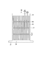
- the region where the lower electrode finger 36 and the upper electrode finger 25 intersect and the lower electrode finger 36 is covered with the upper electrode finger 25 (intersection 28) is a liquid crystal. While not contributing to molecular orientation, it causes an increase in load capacity. Accordingly, in the lower layer electrode 42 of the present embodiment, as shown in FIGS. 12 to 14, a part of the lower layer electrode finger 43 is omitted at the intersection 28 between the lower layer electrode finger 43 and the upper layer electrode finger 25, and rectangular. A shaped opening 44 is provided.
- the dimension H1 of the opening 44 in the extending direction of the lower layer electrode finger 43 is 5 ⁇ m
- the dimension H2 of the opening in the direction orthogonal to the extending direction of the lower layer electrode finger 43 is 3 ⁇ m.
- the widened portion 37 is completely isolated from the lower electrode finger 43 even if the opening 44 is provided. Rather, they are connected in part.
- Other configurations are the same as those in the first and second embodiments.
- the load capacity can be reduced as compared with the conventional FFS type liquid crystal display device, the power consumption required for driving can be reduced, high-speed driving can be performed without any trouble, and the like. Similar effects can be obtained.
- the load capacity when compared with the second embodiment, it is possible to reduce the load capacity without changing the generation state of the transverse electric field and thus without reducing the transmittance.
- the shape of the opening 44 is rectangular, but the shape of the opening 44 is not limited to a rectangular shape and may be changed as appropriate.
- the dimension of the opening 44 may be changed as appropriate.
- a configuration in which an opening is provided at the intersection may be applied.
- FIGS. 15, 16A, and 16B The basic configuration of the liquid crystal display device of this embodiment is the same as that of the first embodiment, and the configuration of the lower layer electrode is different from that of the first embodiment.
- FIG. 15 is a plan view showing one pixel of the liquid crystal display device of this embodiment.
- FIG. 16A is a plan view showing a lower layer electrode.
- FIG. 16B is a plan view showing only the upper layer electrode.
- symbol is attached
- L1 / S1 of the upper electrode finger is 3/3 ⁇ m
- L2 / S2 of the lower electrode finger is 3/3 ⁇ m
- the sum (L1 + S1) of the line width L1 of the upper electrode finger and the interval S1 is the pitch of the upper electrode finger
- the sum of the line width L2 of the lower electrode finger and the interval S2 (L2 + S2) is the pitch of the lower electrode finger. Therefore, in the first to fourth embodiments, the pitch of the upper electrode fingers is equal to the pitch of the lower electrode fingers.
- the pitch of the lower electrode fingers 47 is only made half the pitch of the lower electrode fingers 23 of the first embodiment, and the shape of the lower electrode fingers 47 is the same as that of the first embodiment. It is the same. Other configurations are the same as those in the first embodiment.
- the load capacity can be greatly reduced as compared with the conventional FFS type liquid crystal display device, the power consumption required for driving can be reduced, and high-speed driving can be performed without any trouble. An effect can be obtained.
- the pitch L2 + S2 of the lower electrode fingers 47 is made fine, and the line width L2 of the lower electrode fingers 47 is also made thin. That is, the lower layer electrode fingers 47 whose line width is thinner than that of the first embodiment are densely arranged.
- the lower electrode finger 47 when viewed along the direction orthogonal to the lower electrode finger 47, there is no region where the lower electrode finger 47 is entirely covered by the upper electrode finger 25, and the upper electrode finger 47 is not interposed between the lower electrode finger 47.
- region which 25 adjoins is lost. As a result, the orientation of the liquid crystal molecules is stabilized over the entire pixel region, and high transmittance can be obtained.
- the load capacity does not fluctuate due to misalignment.
- the line width L2 of the lower electrode finger 47 and the interval S2 are set equal, but the pitch (L2 + S2) of the lower electrode finger 47 is larger than the pitch (L1 + S1) of the upper electrode finger 25.
- the line width L2 and the interval S2 of the lower layer electrode finger 47 may be different because it is only necessary to satisfy the condition that it is small.
- the line width L2 of the lower layer electrode finger 47 may be larger than the interval S2, or the line width L2 of the lower layer electrode finger 47 may be smaller than the interval S2.
- FIGS. 17, 18A and 18B The basic configuration of the liquid crystal display device of this embodiment is the same as that of the first embodiment, and the configuration of the lower layer electrode is different from that of the first embodiment.
- FIG. 17 is a plan view showing one pixel of the liquid crystal display device of the present embodiment.
- FIG. 18A is a plan view showing only the lower layer electrode.
- FIG. 18B is a plan view showing only the upper layer electrode.
- the same components as those in FIG. 1 to FIG. 3B of the first embodiment are denoted by the same reference numerals, and description thereof is omitted.
- the pitch of the upper electrode fingers is equal to the pitch of the lower electrode fingers.
- the line width L1 of the upper layer electrode finger and the line width L2 of the lower layer electrode finger are made equal.
- the line width L2 of the lower layer electrode finger 50 is made thicker than the line width L1 of the upper layer electrode finger 25.
- L1 / S1 of the upper electrode finger 25 is 3/3 ⁇ m
- L2 / S2 of the lower electrode finger 50 is 4/2 ⁇ m.
- the line width of the lower electrode finger 50 is only made thicker than the line width of the lower electrode finger 23 of the first embodiment, and the shape of the lower electrode finger 50 is the same as that of the first embodiment. It is the same.
- Other configurations are the same as those in the first embodiment.
- the load capacity can be greatly reduced as compared with the conventional FFS type liquid crystal display device, the power consumption required for driving can be reduced, and high-speed driving can be performed without any trouble. An effect can be obtained.
- FIGS. 19, 20A, and 20B The basic configuration of the liquid crystal display device of this embodiment is the same as that of the first embodiment, and only the configuration of the lower layer electrode is different from that of the first embodiment.
- FIG. 19 is a plan view showing one pixel of the liquid crystal display device of the present embodiment.
- FIG. 20A is a plan view showing only the lower layer electrode.
- FIG. 20B is a plan view showing only the upper layer electrode. 19, FIG. 20A, and FIG. 20B, the same components as those in FIG. 1 to FIG. 3B of the first embodiment are denoted by the same reference numerals, and description thereof is omitted.
- the lower layer electrodes are arranged so that the extending direction of the lower layer electrode fingers is parallel to the source bus lines.
- the lower layer electrode 52 is rotated by 90 ° in the plane of the TFT array substrate 6 from the arrangement of the above embodiment, and the lower layer electrode finger 53 is extended.
- the pitch L2 + S2 of the lower electrode fingers 53 is made smaller than the pitch L1 + S1 of the upper electrode fingers 25.
- L1 / S1 of the upper electrode finger 25 is 3/3 ⁇ m
- L2 / S2 of the lower electrode finger 53 is 1.5 / 1.5 ⁇ m.
- the pitch L2 + S2 of the lower layer electrode finger 53 is set to 1 ⁇ 2 of the pitch L1 + S1 of the upper layer electrode finger 25.
- Other configurations are the same as those in the first embodiment.
- the load capacity can be reduced as compared with the conventional FFS type liquid crystal display device, the power consumption required for driving can be reduced, and high speed driving can be performed without any trouble. Can be obtained.
- interval S2 of the lower layer electrode finger 53 were set equal, the line width L2 and the space
- the line width L2 of the lower layer electrode finger 53 may be larger than the interval S2, and the line width L2 of the lower layer electrode finger 53 may be smaller than the interval S2.
- the present inventors demonstrated the effects of the present invention by simulating the transmittance distribution, the electric field distribution in the liquid crystal layer, the alignment state of the liquid crystal molecules, the pixel capacitance, and the like for the liquid crystal display devices of the above embodiments. The results will be described below.
- the pretilt angle of the liquid crystal layer is 0 °
- the liquid crystal display device of the first embodiment shown in FIG. the pattern of the upper layer electrode and the lower layer electrode shown in FIG. 2 is a repetition of a periodic unit pattern. Therefore, if simulation is performed with unit patterns, it can be easily assumed that simulation results such as transmittance distribution, electric field distribution, and liquid crystal alignment state are also repeated in the pixel. This method is common to all the following embodiments.
- FIGS. 21A and 21B only a part of the electrode patterns in the pixel region is taken out and used as a unit pattern.
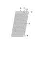
- FIG. 21A shows the lower layer electrode pattern 56 used in the simulation
- FIG. 21B shows the upper layer electrode pattern 57.
- the overlapping area of the upper layer electrode and the lower layer electrode is 50% of the entire electrode formation region, whereas in the first embodiment, the overlapping area of the upper layer electrode and the lower layer electrode is Reduced to 25%.
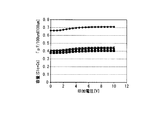
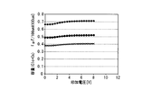
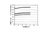
- FIG. 29 is a graph showing the relationship between applied voltage and pixel capacitance (Clc + Cs).
- the relationship between the applied voltage and the pixel capacitance (Clc + Cs) in the first embodiment is indicated by ⁇ .
- the relationship between the voltage applied to the conventional FFS and the pixel capacitance (Clc + Cs) is shown by ⁇ .
- the horizontal axis in FIG. 29 indicates the applied voltage [V].
- the vertical axis in FIG. 29 indicates the pixel capacitance [pF / 100 ⁇ m ⁇ 100 ⁇ m].
- comparison is made by converting to an area of 100 ⁇ 100 ⁇ m 2 .
- the relationship between the applied voltage and the pixel capacitance (Clc + Cs) in the second embodiment is indicated by ⁇ .
- the pixel capacitance can be reduced to 57% in the first embodiment compared to the conventional FFS method.
- the overlapping area between the upper layer electrode and the lower layer electrode can be reduced to 50% of the conventional FFS method
- the pixel capacitance includes capacitances other than the overlapping portion, so the reduction rate is smaller than that. Nevertheless, it has been found that the pixel capacity can be reduced by 43% compared to the conventional FFS method.
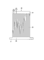
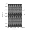
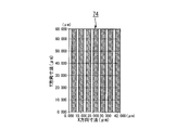
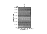
- FIG. 22 shows the transmittance distribution in the patterns shown in FIGS. 21A and 21B.
- a portion that appears white indicates a portion with a high transmittance when an electric field is applied
- a portion that appears black indicates a portion with a low transmittance when an electric field is applied.
- the liquid crystal display device of this embodiment is in a normally black mode, and displays white when an electric field is applied. Therefore, the portion that appears white is a portion where the alignment state of the liquid crystal molecules is good, and the portion that appears black is a portion where the alignment state of the liquid crystal molecules is poor.
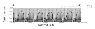
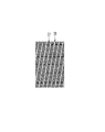
- FIG. 23A is a cross-sectional view of the liquid crystal layer corresponding to this portion, showing equipotential lines and directors of liquid crystal molecules. From the shape of the equipotential lines, it was found that the transverse electric field was sufficiently generated. It was also found that the liquid crystal molecules were sufficiently aligned. On the other hand, since there is no overlap between the upper layer electrode and the lower layer electrode at this location, the load capacity is reduced.
- FIG. 23B is a cross-sectional view of the liquid crystal layer corresponding to this location, showing equipotential lines and directors of liquid crystal molecules. From the shape of the equipotential lines, it was found that the potential of the lower electrode was shielded by the upper electrode, and no transverse electric field was generated. It was also found that the liquid crystal molecules were not aligned. On the other hand, a large load capacitance is formed at this location due to the overlap between the upper layer electrode and the lower layer electrode. In the second and subsequent embodiments, the transmittance at the electrode intersection is improved.
- FIG. 24A shows the lower electrode pattern 59 used in the simulation
- FIG. 24B shows the upper electrode pattern 60.
- the overlapping area of the upper layer electrode and the lower layer electrode is 50% of the entire electrode formation region, whereas in the second example, the upper layer electrode and the upper layer electrode are similar to the first example. The overlapping area with the lower layer electrode was reduced to 25%.
- the relationship between the applied voltage and the pixel capacitance (Clc + Cs) in the second embodiment is indicated by ⁇ .
- the pixel capacity can be reduced to 61% with respect to the conventional FFS system.
- the load capacity due to the transverse electric field is slightly increased by providing the widened portion. Therefore, the reduction effect of the pixel capacity is reduced from 57% to 61% with respect to the conventional FFS system in the first embodiment. Nevertheless, it was found that the pixel capacity can be reduced by 39% compared to the conventional FFS method.
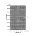
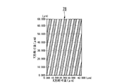
- FIG. 25 shows the transmittance distribution in the patterns shown in FIGS. 24A and 24B. Looking at the location near 1/2 (the location along the line AA ′) from the top of the transmittance distribution diagram of FIG. 25, it looks white in FIG. 22 of the first embodiment, but appears white. It was found that the transmittance was improved.
- FIG. 26 is a cross-sectional view of the liquid crystal layer corresponding to this portion.
- the lower layer electrode is exposed to the side of the upper layer electrode.
- FIG. 23B of the first example it can be seen that the transverse electric field is sufficiently generated and the liquid crystal molecules are sufficiently aligned. It was.
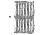
- FIG. 27A shows the lower electrode pattern 62 used in the simulation
- FIG. 27B shows the upper electrode pattern 63.
- the overlapping area of the upper layer electrode and the lower layer electrode is 50% of the entire electrode formation region, whereas in the third example, as in the first and second examples, The overlapping area between the upper layer electrode and the lower layer electrode was reduced to 25%.
- the relationship between the applied voltage and the pixel capacitance (Clc + Cs) in the third embodiment is indicated by *.
- the pixel capacity can be reduced to 63% with respect to the conventional FFS system.
- the overlapping area of the upper layer electrode and the lower layer electrode is the same as in the first and second embodiments, but in addition to providing the widened portion, the edge of the lower layer electrode finger is expanded until it is parallel to the edge of the upper layer electrode finger.
- the load capacity due to the transverse electric field further increased. Therefore, the effect of reducing the pixel capacity is further reduced from 61% to 63% compared to the conventional FFS system in the second embodiment. Nevertheless, it was found that the pixel capacity could be reduced by 37% compared to the conventional FFS method.
- FIG. 28 shows the transmittance distribution in the pattern shown in FIGS. 27A and 27B. Looking at the transmittance distribution diagram of FIG. 28, in FIG. 25 of the second embodiment, even the portion that appeared black at the top and bottom of the 1 ⁇ 2 portion from the top becomes white and the transmittance is further improved. I found out.
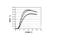
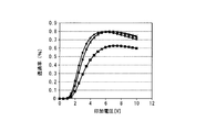
- FIG. 30 is a graph showing the relationship between applied voltage and transmittance in the first to third embodiments.
- the relationship between the applied voltage and the transmittance in the first example is indicated by ⁇ .
- the relationship between the applied voltage and the transmittance in the second example is indicated by ⁇ .
- the relationship between the applied voltage and the transmittance in the third embodiment is indicated by *.
- the relationship between the applied voltage and the transmittance in the conventional FFS method is indicated by ⁇ .
- the horizontal axis in FIG. 30 is the applied voltage [V]
- the vertical axis in FIG. 30 is the transmittance [%].
- the transmittance here is the transmittance of the liquid crystal cell alone without including the polarizing plate.
- the transmittance of the first embodiment is reduced by 20%
- the transmittance of the second embodiment is reduced by 5%
- the transmittance of the third embodiment is compared with the transmittance in the FFS system.
- the rate was found to improve by 3%.
- Table 1 summarizes the calculation results regarding the pixel capacity and transmittance in the first to third embodiments.
- FIG. 31A shows the lower layer electrode pattern 65 used in the simulation
- FIG. 31B shows the upper layer electrode pattern 66.
- the overlapping area of the upper layer electrode and the lower layer electrode is 50% of the entire electrode formation region, whereas in the fourth embodiment, the intersection of the upper layer electrode finger and the lower layer electrode finger By providing the opening in the part, the overlapping area of the upper layer electrode and the lower layer electrode was reduced to 17.5%.
- FIG. 34 is a graph showing the relationship between applied voltage and pixel capacitance (Clc + Cs).
- the relationship between the applied voltage and the pixel capacitance (Clc + Cs) in the fourth embodiment is indicated by x.
- the relationship between the applied voltage and the pixel capacitance (Clc + Cs) in the first embodiment is indicated by ⁇ .
- the relationship between the applied voltage and the pixel capacitance (Clc + Cs) in the conventional FFS method is indicated by ⁇ .
- the horizontal axis in FIG. 34 indicates the applied voltage [V]
- the vertical axis in FIG. 34 indicates the pixel capacitance [pF / 100 ⁇ m ⁇ 100 ⁇ m].
- the pixel capacity can be reduced to 52% in the fourth embodiment compared to the conventional FFS system. Since the overlapping area of the upper layer electrode and the lower layer electrode is reduced as compared with the above embodiment, the pixel capacitance reduction effect is improved from 61% to 52% of the FFS method of the second embodiment, for example. The maximum effect was obtained in the examples.
- FIG. 32 shows the transmittance distribution in the patterns shown in FIGS. 31A and 31B. As in FIG. 25 of the second example, the transmittance was good overall.
- FIG. 33 is a cross-sectional view of the liquid crystal layer corresponding to a half position (a section along the line AA ′) from the top of the transmittance distribution diagram of FIG.
- the fourth example showed a tendency similar to that of FIG. 26 of the second example, and it was found that the transverse electric field was sufficiently generated and the liquid crystal molecules were sufficiently aligned.
- FIG. 35 is a graph showing the relationship between applied voltage and transmittance in the first and fourth examples.
- the relationship between the applied voltage and the transmittance in the first example is indicated by ⁇ .
- the relationship between the applied voltage and the transmittance in the fourth example is indicated by x.
- the relationship between the applied voltage and the transmittance in the conventional FFS method is indicated by ⁇ .
- the horizontal axis in FIG. 35 is the applied voltage [V]
- the vertical axis in FIG. 35 is the transmittance [%].
- the transmittance here is the transmittance of the liquid crystal cell alone without including the polarizing plate.
- the transmittance of the first example was reduced by 20% and the transmittance of the fourth example was reduced by 5% with respect to the transmittance of the FFS method.
- the transmittance of the fourth embodiment is equivalent to the transmittance of the second embodiment.
- Table 2 summarizes the calculation results regarding the pixel capacitance and transmittance in the first and fourth examples.
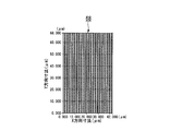
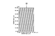
- FIG. 36A shows the lower layer electrode pattern 68 used in the simulation
- FIG. 36B shows the upper layer electrode pattern 69
- FIG. 36C shows the upper layer electrode pattern 69 superimposed on the lower layer electrode pattern 68. It is.
- the pitch of the lower electrode fingers is reduced, so that the lower electrode fingers are always exposed to the side of the upper electrode fingers, and the upper layer fingers are not interposed. There is no longer any place where the electrode fingers are adjacent to each other.
- FIG. 37 shows the transmittance distribution in the patterns shown in FIGS. 36A to 36C.
- the transmittance was substantially uniform and was good overall.
- FIG. 38 is a cross-sectional view of the liquid crystal layer corresponding to a half position (a position along the line AA ′) from the top of the transmittance distribution diagram of FIG. It was found that the transverse electric field was sufficiently generated and the liquid crystal molecules were aligned substantially uniformly.
- FIG. 39 is a graph showing the relationship between applied voltage and pixel capacitance (Clc + Cs).
- the horizontal axis of FIG. 39 indicates the applied voltage [V]
- the vertical axis of FIG. 39 indicates the pixel capacitance [pF / 100 ⁇ m ⁇ 100 ⁇ m].
- L2 / S2 3/3 ⁇ m (corresponding to the first embodiment in which the pitch of the lower electrode finger is not reduced, indicated by ⁇ in FIG. 39)
- the pixel capacity could be reduced to 57% compared to the conventional FFS method.
- the pixel capacity could be reduced to 66% compared to the conventional FFS method.
- FIG. 40 is a graph showing the relationship between applied voltage and transmittance in the fifth example.
- the horizontal axis in FIG. 40 is the applied voltage [V]
- the vertical axis in FIG. 40 is the transmittance [%].
- the transmittance here is the transmittance of the liquid crystal cell alone without including the polarizing plate.
- L2 / S2 1.5 / 1.5 ⁇ m (indicated by ⁇ in FIG. 40)
- L2 / S2 1.0 / 1.0 ⁇ m (FIG. 40).
- the fine upper layer electrode fingers are densely arranged above the lower layer electrode fingers, and the area where the lower layer electrode fingers are exposed is increased. It turned out to be extremely small.
- FIG. 42 shows the transmittance distribution in the patterns shown in FIGS. 41A to 41C.
- the movement of the liquid crystal molecules was extremely small, and the transmittance was lowered. Therefore, as shown in the transmittance distribution diagram of FIG. 42, it was found that many black spots appear periodically.
- FIG. 43 is a cross-sectional view of the liquid crystal layer corresponding to a half position (a position along the line AA ′) from the top of the transmittance distribution diagram of FIG.
- the upper electrode finger virtually functions as a full shield, and the potential of the lower electrode finger does not come out to the liquid crystal layer side. Therefore, the transverse electric field is not sufficiently generated. As a result, it was found that the liquid crystal molecules were not sufficiently aligned.
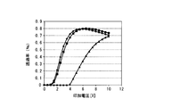
- FIG. 44 is a graph showing the relationship between applied voltage and transmittance in this comparative example.
- the horizontal axis in FIG. 44 is the applied voltage [V], and the vertical axis in FIG. 44 is the transmittance [%].
- the transmittance here is the transmittance of the liquid crystal cell alone without including the polarizing plate.
- the relationship between the applied voltage and the transmittance in this comparative example is indicated by ⁇ .
- the relationship between the applied voltage and the transmittance in the fifth example is indicated by ⁇ .
- the relationship between the applied voltage and the transmittance in the conventional FFS method is indicated by ⁇ .
- FIG. 45A is the lower layer electrode pattern 74 used for the simulation
- FIG. 45B is the upper layer electrode pattern 75
- FIG. 45C is an overlay of the upper layer electrode pattern 75 on the lower layer electrode pattern 74. It is.
- FIG. 45C by increasing the line width of the lower electrode finger without changing the pitch of the lower electrode finger, the lower electrode finger is necessarily exposed to the side of the upper electrode finger. There was no place where the upper electrode fingers were adjacent to each other without the lower electrode fingers intervening.
- FIG. 46 shows the transmittance distribution in the patterns shown in FIGS. 45A to 45C.
- the transmittance was substantially uniform and was good overall.
- FIG. 47 is a cross-sectional view of the liquid crystal layer corresponding to a half point from the top of the transmittance distribution diagram of FIG. It was found that the transverse electric field was sufficiently generated and the liquid crystal molecules were aligned substantially uniformly.
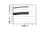
- FIG. 48 is a graph showing the relationship between applied voltage and pixel capacitance (Clc + Cs).
- the horizontal axis in FIG. 48 indicates the applied voltage [V]
- the vertical axis in FIG. 48 indicates the pixel capacitance [pF / 100 ⁇ m ⁇ 100 ⁇ m]. *
- L2 / S2 3/3 ⁇ m (the first embodiment, indicated by x in FIG. 48). Since the area of the overlapping portion between the lower electrode finger and the upper electrode finger is increased by increasing the line width L2 of the lower electrode finger, the pixel capacity is increased. Nevertheless, compared with the conventional FFS method (indicated by ⁇ in FIG. 48), the pixel capacity can be sufficiently reduced.
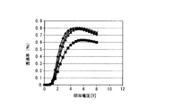
- FIG. 49 is a graph showing the relationship between applied voltage and transmittance in the sixth example.
- the horizontal axis in FIG. 49 is the applied voltage [V]
- the vertical axis in FIG. 49 is the transmittance [%].
- the transmittance here is the transmittance of the liquid crystal cell alone without including the polarizing plate.
- the liquid crystal layer is improved in the alignment state, so that the transmittance is improved as compared with the first example. A substantially equivalent transmittance was obtained.
- FIG. 50A shows the lower layer electrode pattern 77 used for the simulation
- FIG. 50B shows the upper layer electrode pattern 78
- FIG. 50C shows the upper layer electrode pattern 78 superimposed on the lower layer electrode pattern 77. It is.
- the extending direction of the lower layer electrode fingers is different from those in the first to sixth embodiments.
- the pitch of the lower electrode fingers is reduced, and the same operation and effect as the fifth embodiment can be obtained. That is, by lowering the pitch of the lower electrode fingers, the lower electrode fingers are necessarily exposed to the side of the upper electrode fingers, and there is no place where the upper electrode fingers are adjacent to each other without the lower electrode fingers interposed. .
- FIG. 51 shows the transmittance distribution in the patterns shown in FIGS. 50A to 50C.
- the liquid crystal molecules are aligned substantially uniformly, and the transmittance is generally good.
- FIG. 52 is a graph showing the relationship between applied voltage and pixel capacitance (Clc + Cs).
- the horizontal axis in FIG. 52 represents the applied voltage [V]
- the vertical axis in FIG. 52 represents the pixel capacitance [pF / 100 ⁇ m ⁇ 100 ⁇ m].
- the pixel capacity of the seventh embodiment is slightly increased compared to the pixel capacity of the first embodiment.
- the pixel capacity of the seventh embodiment is almost the same as the pixel capacity of the fifth embodiment. Therefore, it has been found that changing the orientation of the lower electrode finger without changing the dimensions does not affect the pixel capacitance.
- FIG. 53 is a graph showing the relationship between applied voltage and transmittance in the seventh example.
- the horizontal axis in FIG. 53 is the applied voltage [V]
- the vertical axis in FIG. 53 is the transmittance [%].
- the transmittance here is the transmittance of the liquid crystal cell alone without including the polarizing plate.
- the seventh example a transmittance substantially equivalent to that of the conventional FFS method was obtained.
- the transmittance of the seventh embodiment is almost the same as the transmittance of the fifth embodiment. Therefore, it was found that the transmittance is not affected even if only the direction of the lower electrode finger is changed unless the dimensions are changed.
- FIG. 54 is a front view showing a schematic configuration of a liquid crystal television which is a configuration example of a liquid crystal display device.
- the liquid crystal television 101 of this configuration example includes the liquid crystal display device 1 of the first to seventh embodiments as a display screen.
- a liquid crystal panel is disposed on the viewer side (front side in FIG. 54), and a backlight (surface light source device) is disposed on the side opposite to the viewer (back side in FIG. 21).
- the liquid crystal television 101 of this configuration example is a liquid crystal television capable of high-quality display by including the liquid crystal display device 1 of the above embodiment.
- liquid crystal display device of the above embodiment can be applied to mobile applications such as portable electronic devices. In that case, a mobile device with low power consumption can be realized.
- the gist of the aspect of the present invention is that each electrode is designed from the beginning so that the lower electrode finger and the upper electrode finger intersect.
- the liquid crystal display device according to the aspect of the present invention is different from a liquid crystal display device manufactured so that, for example, a misalignment in the rotation direction in the substrate plane occurs during the manufacturing process, and the lower electrode finger and the upper electrode finger happen to intersect. Therefore, for example, as shown in FIG. 2, the portions other than the electrode fingers of each electrode, for example, the connection portion are made parallel with the lower layer electrode and the upper layer electrode, and only the electrode finger portions intersect with each other. It is desirable.
- each part of the liquid crystal display device used in the above embodiment or the above examples are not limited to those illustrated in the above embodiment or the above examples, and may be changed as appropriate. Is possible.
- the aspect of the present invention can be used for a liquid crystal display device.
- SYMBOLS 1 Liquid crystal display device, 6 ... TFT array substrate, 7 ... Opposite substrate, 8 ... Liquid crystal layer, 20 ... Upper layer electrode, 22, 35, 39, 42, 46, 49, 52 ... Lower layer electrode, 23, 36, 40, 43, 47, 50, 53 ... lower layer electrode fingers, 25 ... upper layer electrode fingers, 28 ... intersections, 37, 41 ... widened portions, 44 ... openings.
Landscapes
- Physics & Mathematics (AREA)
- Nonlinear Science (AREA)
- Geometry (AREA)
- Mathematical Physics (AREA)
- Chemical & Material Sciences (AREA)
- Crystallography & Structural Chemistry (AREA)
- General Physics & Mathematics (AREA)
- Optics & Photonics (AREA)
- Liquid Crystal (AREA)
- Devices For Indicating Variable Information By Combining Individual Elements (AREA)
Abstract
Priority Applications (2)
| Application Number | Priority Date | Filing Date | Title |
|---|---|---|---|
| US14/122,526 US20140098335A1 (en) | 2011-06-03 | 2012-06-01 | Liquid crystal display device |
| CN201280027205.8A CN103597403B (zh) | 2011-06-03 | 2012-06-01 | 液晶显示装置 |
Applications Claiming Priority (2)
| Application Number | Priority Date | Filing Date | Title |
|---|---|---|---|
| JP2011125186 | 2011-06-03 | ||
| JP2011-125186 | 2011-06-03 |
Publications (1)
| Publication Number | Publication Date |
|---|---|
| WO2012165617A1 true WO2012165617A1 (fr) | 2012-12-06 |
Family
ID=47259468
Family Applications (1)
| Application Number | Title | Priority Date | Filing Date |
|---|---|---|---|
| PCT/JP2012/064277 Ceased WO2012165617A1 (fr) | 2011-06-03 | 2012-06-01 | Dispositif d'affichage à cristaux liquides |
Country Status (4)
| Country | Link |
|---|---|
| US (1) | US20140098335A1 (fr) |
| JP (1) | JPWO2012165617A1 (fr) |
| CN (1) | CN103597403B (fr) |
| WO (1) | WO2012165617A1 (fr) |
Cited By (1)
| Publication number | Priority date | Publication date | Assignee | Title |
|---|---|---|---|---|
| CN103676353A (zh) * | 2013-12-04 | 2014-03-26 | 京东方科技集团股份有限公司 | 像素结构、阵列基板及显示装置 |
Families Citing this family (4)
| Publication number | Priority date | Publication date | Assignee | Title |
|---|---|---|---|---|
| CN102253495B (zh) * | 2010-05-18 | 2013-10-30 | 京东方科技集团股份有限公司 | 双视显示设备和系统 |
| CN105807498A (zh) * | 2016-05-18 | 2016-07-27 | 京东方科技集团股份有限公司 | 一种显示面板及其制作方法和显示装置 |
| CN106154658B (zh) * | 2016-09-26 | 2023-07-07 | 合肥鑫晟光电科技有限公司 | 阵列基板、显示面板、显示装置及显示面板的设计方法 |
| KR102592717B1 (ko) * | 2019-04-30 | 2023-10-23 | 삼성디스플레이 주식회사 | 광학 필름 및 이를 포함하는 표시 패널 |
Citations (3)
| Publication number | Priority date | Publication date | Assignee | Title |
|---|---|---|---|---|
| JP2001056475A (ja) * | 1999-06-29 | 2001-02-27 | Hyundai Electronics Ind Co Ltd | フリンジフィールド駆動液晶表示装置 |
| JP2006350282A (ja) * | 2005-06-14 | 2006-12-28 | Boe Hydis Technology Co Ltd | フリンジフィールドスイッチングモード液晶表示装置 |
| JP2008046599A (ja) * | 2006-08-10 | 2008-02-28 | Samsung Electronics Co Ltd | 表示装置 |
Family Cites Families (7)
| Publication number | Priority date | Publication date | Assignee | Title |
|---|---|---|---|---|
| TW386169B (en) * | 1993-07-27 | 2000-04-01 | Tokyo Shibaura Electric Co | Liquid crystal display apparatus |
| TW451099B (en) * | 1998-01-23 | 2001-08-21 | Hitachi Ltd | Liquid crystal display device |
| TW588171B (en) * | 2001-10-12 | 2004-05-21 | Fujitsu Display Tech | Liquid crystal display device |
| US8174655B2 (en) * | 2006-12-22 | 2012-05-08 | Lg Display Co., Ltd. | Liquid crystal display device and method of fabricating the same |
| JP4693186B2 (ja) * | 2007-12-28 | 2011-06-01 | 株式会社 日立ディスプレイズ | 液晶表示装置 |
| JP5408912B2 (ja) * | 2008-07-02 | 2014-02-05 | 株式会社ジャパンディスプレイ | 液晶表示パネル |
| TWI393968B (zh) * | 2008-12-18 | 2013-04-21 | Au Optronics Corp | 液晶顯示面板 |
-
2012
- 2012-06-01 CN CN201280027205.8A patent/CN103597403B/zh not_active Expired - Fee Related
- 2012-06-01 WO PCT/JP2012/064277 patent/WO2012165617A1/fr not_active Ceased
- 2012-06-01 JP JP2013518188A patent/JPWO2012165617A1/ja active Pending
- 2012-06-01 US US14/122,526 patent/US20140098335A1/en not_active Abandoned
Patent Citations (3)
| Publication number | Priority date | Publication date | Assignee | Title |
|---|---|---|---|---|
| JP2001056475A (ja) * | 1999-06-29 | 2001-02-27 | Hyundai Electronics Ind Co Ltd | フリンジフィールド駆動液晶表示装置 |
| JP2006350282A (ja) * | 2005-06-14 | 2006-12-28 | Boe Hydis Technology Co Ltd | フリンジフィールドスイッチングモード液晶表示装置 |
| JP2008046599A (ja) * | 2006-08-10 | 2008-02-28 | Samsung Electronics Co Ltd | 表示装置 |
Cited By (2)
| Publication number | Priority date | Publication date | Assignee | Title |
|---|---|---|---|---|
| CN103676353A (zh) * | 2013-12-04 | 2014-03-26 | 京东方科技集团股份有限公司 | 像素结构、阵列基板及显示装置 |
| CN103676353B (zh) * | 2013-12-04 | 2016-07-06 | 京东方科技集团股份有限公司 | 像素结构、阵列基板及显示装置 |
Also Published As
| Publication number | Publication date |
|---|---|
| JPWO2012165617A1 (ja) | 2015-02-23 |
| CN103597403B (zh) | 2016-03-30 |
| CN103597403A (zh) | 2014-02-19 |
| US20140098335A1 (en) | 2014-04-10 |
Similar Documents
| Publication | Publication Date | Title |
|---|---|---|
| JP5756860B2 (ja) | 液晶ディスプレイ | |
| US10134906B2 (en) | Display device | |
| JP6116220B2 (ja) | 液晶表示パネル | |
| JP5695946B2 (ja) | 液晶表示装置 | |
| US8004644B2 (en) | Liquid crystal display device | |
| JP5906043B2 (ja) | 液晶表示装置 | |
| JP5555663B2 (ja) | 液晶表示装置 | |
| CN101620346A (zh) | 液晶显示面板 | |
| US9891479B2 (en) | Liquid crystal display device including a pixel electrode and a common electrode | |
| WO2014054500A1 (fr) | Dispositif d'affichage à cristaux liquides | |
| CN103597403B (zh) | 液晶显示装置 | |
| JP5078176B2 (ja) | 液晶表示装置 | |
| JP4516432B2 (ja) | 液晶表示装置 | |
| JP5616841B2 (ja) | 液晶表示装置 | |
| JP6742738B2 (ja) | 液晶表示装置 | |
| US7528894B2 (en) | LCD having storage capacitor electrodes with wider portions located within triangular areas of pixel regions and with spacers disposed in regions corresponding to the triangular areas to mitigate dark-state light leakage | |
| JP5258345B2 (ja) | 液晶表示装置 | |
| JP2010096796A (ja) | 液晶表示装置及び電子機器 | |
| JP5677923B2 (ja) | 液晶表示装置 | |
| JP5197873B2 (ja) | 液晶表示装置 | |
| JP5154597B2 (ja) | 液晶表示装置 | |
| JP2008065212A (ja) | 液晶表示パネル | |
| JP5305271B2 (ja) | 液晶表示装置 | |
| JP2015227981A (ja) | 表示装置 | |
| WO2013083030A1 (fr) | Substrat de réseau et dispositif d'affichage à cristaux liquides |
Legal Events
| Date | Code | Title | Description |
|---|---|---|---|
| WWE | Wipo information: entry into national phase |
Ref document number: 201280027205.8 Country of ref document: CN |
|
| 121 | Ep: the epo has been informed by wipo that ep was designated in this application |
Ref document number: 12793987 Country of ref document: EP Kind code of ref document: A1 |
|
| WWE | Wipo information: entry into national phase |
Ref document number: 14122526 Country of ref document: US |
|
| ENP | Entry into the national phase |
Ref document number: 2013518188 Country of ref document: JP Kind code of ref document: A |
|
| NENP | Non-entry into the national phase |
Ref country code: DE |
|
| 122 | Ep: pct application non-entry in european phase |
Ref document number: 12793987 Country of ref document: EP Kind code of ref document: A1 |