WO2012165656A1 - Dispositif de guide d'onde optique, interféromètre optique, et procédé de production de dispositif de guide d'onde optique - Google Patents
Dispositif de guide d'onde optique, interféromètre optique, et procédé de production de dispositif de guide d'onde optique Download PDFInfo
- Publication number
- WO2012165656A1 WO2012165656A1 PCT/JP2012/064608 JP2012064608W WO2012165656A1 WO 2012165656 A1 WO2012165656 A1 WO 2012165656A1 JP 2012064608 W JP2012064608 W JP 2012064608W WO 2012165656 A1 WO2012165656 A1 WO 2012165656A1
- Authority
- WO
- WIPO (PCT)
- Prior art keywords
- optical waveguide
- optical
- light
- loss
- signals
- Prior art date
- Legal status (The legal status is an assumption and is not a legal conclusion. Google has not performed a legal analysis and makes no representation as to the accuracy of the status listed.)
- Ceased
Links
Images




Classifications
-
- G—PHYSICS
- G02—OPTICS
- G02F—OPTICAL DEVICES OR ARRANGEMENTS FOR THE CONTROL OF LIGHT BY MODIFICATION OF THE OPTICAL PROPERTIES OF THE MEDIA OF THE ELEMENTS INVOLVED THEREIN; NON-LINEAR OPTICS; FREQUENCY-CHANGING OF LIGHT; OPTICAL LOGIC ELEMENTS; OPTICAL ANALOGUE/DIGITAL CONVERTERS
- G02F1/00—Devices or arrangements for the control of the intensity, colour, phase, polarisation or direction of light arriving from an independent light source, e.g. switching, gating or modulating; Non-linear optics
- G02F1/01—Devices or arrangements for the control of the intensity, colour, phase, polarisation or direction of light arriving from an independent light source, e.g. switching, gating or modulating; Non-linear optics for the control of the intensity, phase, polarisation or colour
- G02F1/011—Devices or arrangements for the control of the intensity, colour, phase, polarisation or direction of light arriving from an independent light source, e.g. switching, gating or modulating; Non-linear optics for the control of the intensity, phase, polarisation or colour in optical waveguides, not otherwise provided for in this subclass
-
- G—PHYSICS
- G02—OPTICS
- G02F—OPTICAL DEVICES OR ARRANGEMENTS FOR THE CONTROL OF LIGHT BY MODIFICATION OF THE OPTICAL PROPERTIES OF THE MEDIA OF THE ELEMENTS INVOLVED THEREIN; NON-LINEAR OPTICS; FREQUENCY-CHANGING OF LIGHT; OPTICAL LOGIC ELEMENTS; OPTICAL ANALOGUE/DIGITAL CONVERTERS
- G02F1/00—Devices or arrangements for the control of the intensity, colour, phase, polarisation or direction of light arriving from an independent light source, e.g. switching, gating or modulating; Non-linear optics
- G02F1/01—Devices or arrangements for the control of the intensity, colour, phase, polarisation or direction of light arriving from an independent light source, e.g. switching, gating or modulating; Non-linear optics for the control of the intensity, phase, polarisation or colour
- G02F1/0121—Operation of devices; Circuit arrangements, not otherwise provided for in this subclass
- G02F1/0123—Circuits for the control or stabilisation of the bias voltage, e.g. automatic bias control [ABC] feedback loops
-
- G—PHYSICS
- G02—OPTICS
- G02F—OPTICAL DEVICES OR ARRANGEMENTS FOR THE CONTROL OF LIGHT BY MODIFICATION OF THE OPTICAL PROPERTIES OF THE MEDIA OF THE ELEMENTS INVOLVED THEREIN; NON-LINEAR OPTICS; FREQUENCY-CHANGING OF LIGHT; OPTICAL LOGIC ELEMENTS; OPTICAL ANALOGUE/DIGITAL CONVERTERS
- G02F1/00—Devices or arrangements for the control of the intensity, colour, phase, polarisation or direction of light arriving from an independent light source, e.g. switching, gating or modulating; Non-linear optics
- G02F1/01—Devices or arrangements for the control of the intensity, colour, phase, polarisation or direction of light arriving from an independent light source, e.g. switching, gating or modulating; Non-linear optics for the control of the intensity, phase, polarisation or colour
- G02F1/21—Devices or arrangements for the control of the intensity, colour, phase, polarisation or direction of light arriving from an independent light source, e.g. switching, gating or modulating; Non-linear optics for the control of the intensity, phase, polarisation or colour by interference
- G02F1/225—Devices or arrangements for the control of the intensity, colour, phase, polarisation or direction of light arriving from an independent light source, e.g. switching, gating or modulating; Non-linear optics for the control of the intensity, phase, polarisation or colour by interference in an optical waveguide structure
-
- H—ELECTRICITY
- H04—ELECTRIC COMMUNICATION TECHNIQUE
- H04B—TRANSMISSION
- H04B10/00—Transmission systems employing electromagnetic waves other than radio-waves, e.g. infrared, visible or ultraviolet light, or employing corpuscular radiation, e.g. quantum communication
- H04B10/50—Transmitters
- H04B10/501—Structural aspects
- H04B10/503—Laser transmitters
- H04B10/505—Laser transmitters using external modulation
- H04B10/5057—Laser transmitters using external modulation using a feedback signal generated by analysing the optical output
Definitions
- the present invention relates to an optical waveguide device, an optical interferometer, and an optical waveguide device control method.
- the capacity is increased by increasing the speed and wavelength multiplexing.
- wavelength division multiplexing is widely used in trunk optical communication systems.
- the wavelength channel interval is determined. If the wavelength channel interval in the band of the optical fiber amplifier is 50 GHz, about 100 channels can be used.
- optical multilevel modulation the amount of information is increased without expanding the frequency use band by making the amplitude and phase of light not only binary of “0” and “1” but also multilevel.
- optical OFDM an OFDM signal is generated from an electrical signal, optically modulated, and multiplexed between optical subcarriers in an orthogonal state.
- optical OFDM can reduce problems caused by crosstalk and increase frequency utilization efficiency.
- the digital data to be modulated is transmitted in a multi-valued and multiplexed manner by such processing mainly using electric signals.
- the transmitted optical signal is demodulated into an electrical signal on the receiving side.
- the optical modulation circuit of the optical transmitter requires a digital / analog (D / A) converter and an optical modulator in order to convert digital data, which is an electrical signal, into an optical analog signal waveform.
- D / A digital / analog
- the Mach-Zehnder interferometer is realized as an optical waveguide using, for example, lithium niobate (LiNbO 3 ) as a material.
- FIG. 12 shows a configuration diagram of an LN modulator related to the present invention.
- the light is input from the optical input port 2 of the LN modulator 300 to the optical splitter 3 and output to the first optical waveguide 4 and the second optical waveguide 5.
- Electrodes are formed on part of the first optical waveguide 4 and the second optical waveguide 5.
- transmits an optical waveguide can be changed by applying a voltage to an electrode.
- these will be referred to as a first phase modulator 17 and a second phase modulator 27, respectively.
- the light output from the first optical waveguide 4 and the second optical waveguide 5 is input to the optical coupler 8, and from the optical coupler 8 to the first optical output port 30 and the second optical output port 31. Is output.
- the LN modulator 300 applies a voltage to the first phase modulator 17 or the second phase modulator 27 to change the phase of light transmitted through the waveguide.
- the intensity of the light output from the first and second light output ports 30 and 31 can be changed by the light interference effect in the optical coupler 8.
- an optical modulation function similar to that of the LN modulator 300 shown in FIG. 12 can be realized using an optical waveguide made of a semiconductor material.
- indium phosphide (InP) and indium gallium arsenide (InGaAsP) materials, or gallium arsenide (GaAs) and aluminum gallium arsenide (AlGaAs) materials have been proposed.
- an optical modulator in which a Mach-Zehnder interferometer is composed of these semiconductor materials has been proposed.
- an optical modulator using a semiconductor material can reduce the operating voltage to a fraction of that of an LN modulator, and can further reduce the size to one-tenth or less.
- Patent Documents 1 to 3 disclose a configuration in which a part of an optical signal is monitored by a photodiode (PD) disposed outside. This suppresses characteristic deterioration during operation of the optical modulator.
- Patent Document 4 discloses a configuration of an optical FSK / SSB modulator capable of adjusting the intensity of an optical signal output from a sub Mach-Zehnder waveguide.
- Patent Document 5 discloses a configuration of an optical modulator including a Mach-Zehnder waveguide for intensity adjustment.
- the PD for monitoring the light transmitted through the optical waveguide is generally arranged outside the optical modulator, or is monolithically integrated inside the optical modulator as disclosed in Patent Document 3. Even in the case of integration, it is necessary to monitor the signal output from the Mach-Zehnder interferometer (portion on the output side from the optical coupler).
- the LN modulator 300 shown in FIG. 12 in order to know the light intensity transmitted through the first optical waveguide 4 and the second optical waveguide 5, the light emitted from the end portion of the waveguide is monitored. The light intensity inside the optical waveguide cannot be directly known. For this reason, the LN modulator 300 shown in FIG.
- the first optical output port 30 or the minimum value of the intensity of light output from the second optical output port 31 is completely zero. That is, in this case, the extinction ratio (ON / OFF ratio of the optical signal) is infinite. However, in practice, the extinction ratio of the light output from the optical waveguide may not be infinite but may be a finite value. The cause will be described below.
- the first cause is that the optical intensity branching ratio of the optical branch circuit 3 may not be strictly 1: 1 due to the manufacturing error and wavelength dependency of the optical waveguide.
- the second cause is that the bias voltages applied to the first optical waveguide 4 and the second optical waveguide 5 at the time of phase modulation are different, so that the first optical waveguide 4 and the second optical waveguide 5 are different.
- the optical waveguide loss is also different. That is, when performing phase modulation, the bias voltages of the first phase modulator 17 and the second phase modulator 27 are generally different. For this reason, a difference occurs in the loss of the first optical waveguide 4 and the second optical waveguide 5.
- the loss between the first optical waveguide 4 and the second optical waveguide 5 may gradually differ due to changes in the characteristics of the optical waveguide over time.
- Patent Document 5 discloses a configuration in which a Mach-Zehnder interferometer for adjusting the light intensity is arranged separately from that for modulation to adjust the light intensity, and the light is branched and monitored at the front stage of the optical coupler.
- Patent Document 5 the light intensity is adjusted by monitoring the branched light with a PD and performing feedback control.
- an optical modulator composed of a semiconductor material the phase and loss change simultaneously by applying a voltage to the electrode provided in the optical waveguide. Therefore, it is impossible to adjust only the loss by using a Mach-Zehnder interferometer for intensity modulation as in Patent Document 5.
- the optical modulator described in Patent Document 5 has a problem that the configuration is complicated because the Mach-Zehnder interferometer for intensity modulation is arranged.
- the techniques described in Patent Documents 1 to 4 also disclose a configuration for independently controlling the phase difference and loss of light transmitted through two optical waveguide devices composed of semiconductor materials with a simple configuration. Not done.
- the phase change and the loss change that occur in the optical waveguide provided with two electrodes to which two signals are respectively applied and the light that is transmitted through the optical waveguide by the two signals become predetermined values.
- the control method of the optical waveguide device of the present invention performs control so that a predetermined phase change and loss change occur in light transmitted through the optical waveguide by two signals applied to the optical waveguide having two electrodes, respectively.
- the present invention makes it possible to independently control the phase difference and loss of light transmitted through a plurality of optical waveguide devices with a simple configuration.
- FIG. 3 is a layout diagram of control electrodes in the first embodiment. It is a figure which shows the isoline which the sum total of (DELTA) n in 1st Embodiment is constant. It is a figure which shows the isoline which is the sum total of (DELTA) (alpha) in 1st Embodiment. It is the figure which superposed
- an optical waveguide device that evenly balances the light intensity while giving a desired phase difference between the first optical waveguide and the second optical waveguide of the semiconductor Mach-Zehnder optical modulator. Propose a configuration.
- the light intensity transmitted through the waveguide is monitored at a position before the optical coupler with respect to the traveling direction of the light to be modulated, and the first and second light intensity is monitored based on the monitored light intensity.
- the voltage provided at the electrode of the optical waveguide is controlled. A specific configuration example is shown in FIG.
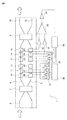
- FIG. 1 is a diagram showing a configuration of an optical waveguide device according to a first embodiment of the present invention.
- the optical waveguide device according to the first embodiment constitutes an optical modulator 1 having a basic configuration of a Mach-Zehnder interferometer (MZI, Mach-Zehnder Interferometer).
- MZI Mach-Zehnder Interferometer
- FIG. 1 light input from the optical input port 2 passes through the optical splitter 3.
- the optical branching device 3 divides the intensity of light into a ratio of about 1: 1 and outputs it to the first optical waveguide 4 and the second optical waveguide 5.
- a 2 ⁇ 2 multi-mode interference (MMI, Multi-Mode Interference) branching device may be used as the optical branching device 3.
- MMI Mach-Zehnder Interferometer
- the phases of the light output to the first optical waveguide 4 and the second optical waveguide 5 are different from each other by 90 degrees.
- the optical branching device 3 is, for example, a Y branch circuit
- the light output to the first optical waveguide 4 and the second optical waveguide 5 is output in the same phase.
- the configuration of the optical branching device 3 is not particularly limited.
- electrodes 10 to 15 and electrodes 20 to 25 are added, respectively. Of these electrodes, the electrodes 10 to 12 and the electrodes 20 to 22 are used for light modulation.
- the refractive index of the optical waveguide in which the electrodes are formed can be changed.
- the phase of the transmitted light can be changed by changing the refractive index of the optical waveguide.
- the light transmitted through the first optical waveguide 4 and the second optical waveguide 5 is input to the optical coupler 8 respectively.
- the light is output from the optical coupler 8 to the first optical output port 30 and the second optical output port 31.
- the intensity ratio of the light output to the first optical output port 30 and the second optical output port 31 is input from the first optical waveguide 4 and the second optical waveguide 5 to the optical coupler 8. It is determined by the phase difference of light.
- the optical branching device 3 and the optical coupler 8 are MMI
- a phase difference of 90 degrees is given to the optical branching device 3 and the optical coupler 8 as described above. Therefore, if the intensity of light input to the optical coupler 8 from the first optical waveguide 4 and the second optical waveguide 5 is equal and the phase difference generated in the optical waveguides 4 and 5 is 0 degree, the optical waveguide All light is output to 31. This is because the path length from the optical input port 2 to the optical output port 31 becomes equal including the phase difference regardless of which of the optical waveguide 4 and the optical waveguide 5 is passed.
- the first optical output Light is output to the port 30 and the second light output port 31 at a light intensity ratio of 1: 1. Further, if the light intensities from the first optical waveguide 4 and the second optical waveguide 5 are equal and the phase difference generated in the first optical waveguide 4 and the second optical waveguide 5 is 180 degrees, the light output All light is output to the port 30. That is, when the intensity of light input to the optical coupler 8 is equal, the light intensity branched to the first optical output port 30 and the second optical output port 31 is controlled by controlling the phase difference therebetween. Can be changed.
- the optical modulator 1 includes electrodes 10 to 15 and electrodes 20 to 25 divided into a plurality of parts. A part of the divided electrodes is used for characteristic control of the first optical waveguide 4 and the second optical waveguide 5.
- the electrodes 15 and 25 are used as monitoring electrodes in order to monitor the respective light intensities input from the first optical waveguide 4 and the second optical waveguide 5 to the optical coupler 8. It is done.
- the electrode By applying a reverse bias voltage to the electrode 15 and the electrode 25, the electrode absorbs light transmitted through the optical waveguide in the vicinity thereof, and generates a light absorption current. Since the magnitude of the light absorption current depends on the light intensity of the transmitted light, the light intensity transmitted through the optical waveguide can be monitored from the magnitude of the light absorption current.
- an electrode for generating a light absorption current is referred to as a “monitor electrode”.
- electrodes 13, 14, 23, and 24 for applying a voltage to the first optical waveguide 4 and the second optical waveguide 5 based on the signal processing result of a DSP (digital signal processor) 34 described below are referred to as “ It is called “control electrode”.
- the electrodes 10 to 12 and 20 to 22 used for actually modulating the light and the electrodes 13 to 15 and 23 to 25 for controlling the optical waveguide characteristics have the same basic structure. May be.
- the structural difference between the electrode used for modulation and the electrode used for controlling the characteristics of the optical waveguide may be about the pattern of the electrode.
- the optical modulator 1 can be easily manufactured.
- Transimpedance amplifiers (hereinafter referred to as TIA) 16 and 26 are electrically connected to the electrode 15 and the electrode 25 which are monitor electrodes, respectively. The TIA amplifies the light absorption current, converts it into a voltage, and outputs it to the differential amplifier 32.
- the differential amplifier 32 generates a voltage signal corresponding to the difference between the voltages output from the TIAs 16 and 26 and outputs the voltage signal to the A / D converter 33.
- the A / D converter 33 outputs the voltage signal output from the differential amplifier 32 to the DSP 34.
- TIA16, TIA26, the differential amplifier 32, and the A / D converter 33 should just be able to process the temporal average value of the light intensity which permeate
- a signal output from the A / D converter 33 is input to the DSP 34 and subjected to signal processing.
- the DSP 34 applies to the electrodes 13, 14, 23, and 24, which are control electrodes, so that the light intensities input from the first optical waveguide 4 and the second optical waveguide 5 to the optical coupler 8 are equalized.
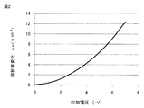
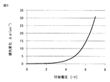
- Determine the voltage value. 2 and 3 show examples of refractive index change and loss change when a voltage is applied to the semiconductor optical modulator, respectively. As shown in FIGS.
- the refractive index change and the loss change of the optical waveguide are independently controlled by applying different voltages to the plurality of electrodes. Below, the example of the procedure which controls the voltage applied to an electrode is shown. In FIG. 2, the refractive index change is ⁇ n (V), and in FIG. 3, the loss change is ⁇ (V).
- (V) indicates that variables such as ⁇ n and ⁇ are functions of the voltage V applied to the electrodes.
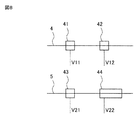
- FIG. 4 is a layout diagram of control electrodes in the first embodiment.
- the electrode 13 and the electrode 14 the electrode 23 and the electrode 24 are used as control electrodes, and the control voltages applied to the electrodes are sequentially V11, V12, V21, V22.
- the refractive index change ⁇ n and the loss change ⁇ that the first optical waveguide 4 and the second optical waveguide 5 receive by applying a voltage to the electrodes 13, 14, 23, and 24 are sequentially expressed as “ ⁇ n11, ⁇ 11”, “ ⁇ n12, ⁇ 12 ”,“ ⁇ n21, ⁇ 21 ”,“ ⁇ n22, ⁇ 22 ”.
- FIG. 5 shows the voltage applied to two electrodes connected in series by a waveguide on the horizontal axis and the vertical axis, respectively, and the sum of ⁇ n generated by these electrodes (the total amount of phase change) is constant.
- An isoline is shown.
- the contour lines in FIG. 5 indicate the trajectories of V11 and V12 where ⁇ n11 + ⁇ n12 is constant as the entire first optical waveguide 4.
- the isoline shown in FIG. 5 shows the trajectories of V21 and V22 where ⁇ n21 + ⁇ n22 is constant as the second optical waveguide 5 as a whole. That is, FIG.
- FIG. 5 shows that the voltage applied to one electrode is increased along the isoline, and the voltage applied to the other electrode is decreased, so that the sum of ⁇ n with respect to light transmitted through the optical waveguide (the amount of phase change) (Total) can be controlled so as not to change.
- the amount of phase change (Total)
- FIG. 6 shows the voltage applied to two electrodes connected in series with a waveguide on the horizontal axis and the vertical axis, respectively, and the sum of ⁇ generated by these electrodes (total loss change amount) is constant. It is a figure which shows an isoline.
- FIG. 6 shows an isoline where ⁇ 21 + ⁇ 22 is constant. That is, in FIG. 6, the voltage applied to one electrode is increased along the isoline, and the voltage applied to the other electrode is decreased, whereby the first optical waveguide 4 and the second optical waveguide 5 are reduced. It shows that the phase of light transmitted through the optical waveguide can be controlled so that the loss does not change.
- FIG. 7 is a diagram in which FIG. 5 and FIG. 6 are superimposed. In FIG.
- a solid line N is an isoline where the sum of ⁇ n is constant
- a broken line is an isoline where ⁇ is constant.
- Point A indicates the set voltage of the voltages V11 and V12
- point B indicates the set voltage of the voltages V21 and V22.
- the first optical waveguide 4 and the second optical waveguide 5 are 1 cm in length.
- the position of points A and B on the solid line N is 1 cm.
- the voltages V11, V12, V21 and V22 may be set so as to be on the broken lines P and Q.
- the voltage values at points A and B are as follows.
- V11 3.6V
- V12 4.6V
- V21 4.0V
- V22 4.0V
- the difference of the total value of ⁇ is 1cm -1
- the voltages at the intersections of the different broken lines P and Q and the solid line N may be set as the voltages V11, V12, V21, and V22.
- the loss difference between the first optical waveguide 4 and the second optical waveguide 5 can be set while maintaining a phase difference different from that in FIG.
- the DSP 34 stores data corresponding to FIG. As described above, the DSP 34 applies the voltage V11 applied to the control electrode so as to generate a predetermined loss difference while keeping the phase constant between the first optical waveguide 4 and the second optical waveguide 5. V12, V21 and V22 are determined. At this time, the DSP 34 desires the light intensity input from the first optical waveguide 4 and the second optical waveguide 5 to the optical coupler 8 based on the difference between the light absorption currents generated in the electrode 15 and the electrode 25, respectively. The voltage to be applied to the control electrode is obtained by calculation so that the ratio becomes (for example, the same).
- the DSP 34 loses the loss of the first optical waveguide 4 and the second optical waveguide 5 under the condition that the difference in phase change applied to the first optical waveguide 4 and the second optical waveguide 5 is constant.
- a driver 35 for amplifying the applied voltage may be provided between the DSP 34 and each electrode.
- the loss of the portion where the electrodes 10 to 12 of the first optical waveguide 4 or the electrodes 20 to 22 of the second optical waveguide 5 are provided increases when these electrodes are used for light modulation over a long period of time. There is a case. If the amount of increase in loss between the first optical waveguide 4 and the second optical waveguide 5 is different, the light intensity input from the first optical waveguide 4 and the second optical waveguide 5 to the optical coupler 8 is increased.
- the DSP 34 uses the voltages V11 and V12 such that the intensity of the light input to the optical coupler 8 becomes a desired value based on the difference between the light absorption currents generated in the electrode 15 and the electrode 25. V21 and V22 may be obtained and applied to the control electrode.
- the optical modulator 1 of the first embodiment can reduce the intensity of light input to the optical coupler 8 even when the loss of the first optical waveguide 4 or the second optical waveguide 5 changes with time. Control can be performed so as to obtain a predetermined ratio.
- the optical coupler is similarly used.
- the light intensity input to 8 can be controlled to a predetermined ratio.
- the optical modulator 1 monitors the intensity of light transmitted through the first optical waveguide 4 and the second optical waveguide 5 so that the ratio becomes a desired value.
- the voltage applied to the electrodes 13, 14, 23 and 24 is controlled.
- the DSP 34 is an isoline whose sum of ⁇ n is constant so that the voltage output from the differential amplifier 32 becomes zero.
- a voltage applied to the control electrode is calculated and output along As a result, in the optical modulator 1 of the first embodiment, it is possible to equalize the intensity of light transmitted through the first optical waveguide and the second optical waveguide without causing a phase change.
- the magnitude of the light absorption current with respect to the light intensity in the optical waveguide differs depending on the electrode. This may cause an error in the characteristic control of the optical waveguide. For this reason, the magnitude of the light absorption current with respect to the light intensity in the optical waveguide may be measured in advance and given to the DSP 34 as correction data.
- the light intensity in the optical waveguide can be more accurately controlled by correcting the variation in the light absorption rate between the electrodes based on the correction data.
- the sum of ⁇ n (phase change) is made constant and the sum of ⁇ (loss change) is controlled.
- the embodiment will be described in the section of the third embodiment. Heretofore, the characteristic control of the optical waveguide in the optical modulator 1 of the first embodiment has been described.
- the light modulation electrodes 10 to 12 and 20 to 22 have basically the same structure as the electrodes 13 to 15 and the electrodes 23 to 25.
- a control circuit that generates voltages to be applied to the electrodes 10 to 12 and the electrodes 20 to 22 is integrated as a modulation circuit 36 and a driver 37. With such a configuration, the light modulator 1 of the first embodiment can realize a compact light modulation circuit including the light modulator and the control circuit.
- the optical waveguide in addition to a general compound semiconductor, can be made of a material whose absorption changes with a change in refractive index, for example, a material such as silicon or germanium.
- the optical waveguide device according to the first embodiment provides light to the optical coupler while giving a desired phase difference to the light transmitted through the optical waveguide included in the Mach-Zehnder optical modulator made of a semiconductor material. It is possible to balance the input intensity evenly. As a result, the optical waveguide device of the first embodiment can improve the extinction ratio of the light output from the optical modulator. That is, the optical waveguide device of the first embodiment can independently control the phase difference and loss of light transmitted through a plurality of optical waveguide devices with a simple configuration.
- the monitoring electrode 15 is disposed between the electrode 14 and the optical coupler 8.
- the position of the monitoring electrode may be on the same waveguide.
- the electrode 15 is located close to the optical coupler 8.
- electrodes at other positions can be used as the monitoring electrode.
- the position of the electrode 25 is the same as that of the electrode 15. 2, 3, and 5 to 7, the case where the characteristics of the first optical waveguide 4 and the second optical waveguide 5 are the same has been described.
- the DSP 34 stores the respective characteristic data, and the voltages V11, V12, V21 and the like based on the respective characteristic data. V22 may be calculated. Further, the position of the electrode to which the voltage is applied by the DSP 34 may be freely set as long as the relationship between the applied voltage and the light intensity input to the optical coupler 8 can be grasped.
- the electrodes for light modulation are electrodes 10 to 12 and electrodes 20 to 22, but the number of electrodes used for light modulation is not limited to this.
- the optical waveguide device is applied to a Mach-Zehnder type optical modulator has been shown.
- the application mode of the optical modulator described in the first embodiment is not limited thereto.
- the configuration of the optical waveguide device according to the first embodiment can be generally applied to an optical waveguide device in which phase change and loss change are to be controlled independently between two semiconductor optical waveguides.
- [Second Embodiment] Next, a second embodiment of the present invention will be described.
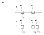
- the optical waveguide device of the second embodiment is obtained by changing the shape of the control electrode provided in the optical waveguides 4 and 5 in the optical waveguide device of the first embodiment shown in FIG. 8 and 9 show the shape of the electrode of the optical waveguide device of the second embodiment. 8 and 9 show only the electrodes 41 to 46 in place of the electrodes 13, 14, 23, and 24 provided in the first and second optical waveguides 4 and 5 in FIG. 1.
- the configuration of the optical waveguide device of the second embodiment is the same as that of the optical waveguide device of the first embodiment except that the electrodes 41 to 46 are provided instead of the electrodes 13, 14 and 23, 24.
- the first optical waveguide 4 includes electrodes 41 and 42 having substantially the same length.
- the second optical waveguide 5 includes electrodes 43 and 44 having different lengths in the light traveling direction.
- FIG. 9 shows a configuration in which the first optical waveguide 5 includes three electrodes 43, 45, and 46 as control electrodes.
- V 23 is a voltage applied to the electrode 46.
- the electrode 45 and the electrode 46 are substantially It operates as a control electrode having a total length. Therefore, the optical waveguide device having the configuration shown in FIG. 9 can perform loss control similar to that of the optical waveguide device shown in FIG.
- the optical waveguide device of the second embodiment independently controls the phase difference and loss of light transmitted through a plurality of optical waveguide devices with a simple configuration, like the optical waveguide device of the first embodiment. Make it possible.
- the length of the electrode can be freely set in the first optical waveguide 5 of the optical waveguide device shown in FIG.
- the number of electrodes is not limited to three. As described above, the length and number of the electrodes are not limited to those shown in FIGS.
- the optical waveguide includes a plurality of electrodes, there is no limitation on the combination of electrodes as long as a voltage can be applied to two or more electrodes for each optical waveguide.
- the optical waveguide device of the second embodiment is configured as an optical modulator by combining the monitor unit for generating the light absorption current described in the first embodiment and the control circuit for applying a voltage to the electrodes 41 to 46. It is also possible to do.
- FIG. 10 is a diagram illustrating the configuration of the optical waveguide device according to the third embodiment.
- the optical waveguide device shown in FIG. 10 is an I / Q (inphase / quadture) modulator 50 in which two Mach-Zehnder optical modulators are connected in parallel.
- the I / Q modulator modulates an I component (real axis) and a Q component (imaginary axis) of an optical signal independently, and performs multi-level modulation by adding information on amplitude and phase on a complex plane.
- the I / Q modulator 50 includes an optical splitter 51, an I modulator 52, a Q modulator 53, and an optical coupler 55.
- Each of the I modulator 52 and the Q modulator 53 constitutes a Mach-Zehnder optical modulator.
- Electrodes 541 to 546 are provided between the outputs of the I modulator 52 and Q modulator 53 and the optical coupler 55.
- the light that is approximately equally divided by the first branching unit 51 is input to the I modulator 52 and the Q modulator 53.
- the I modulator 52 and the Q modulator 53 modulate the input light independently.
- the respective signals modulated by the I modulator 52 and the Q modulator 53 are changed.
- the phase difference needs to be 90 ° at the input of the optical coupler 55. Therefore, in general, a phase shifter that provides a 90 ° phase shift is disposed between one of the I modulator 52 and the Q modulator and the optical coupler 55.
- a phase shifter that provides a 90 ° phase shift is disposed between one of the I modulator 52 and the Q modulator and the optical coupler 55.
- a loss change also occurs in the modulation signal to which the phase shift is given.
- the I / Q modulator 50 includes electrodes 541 to 546 between the output of the I modulator 52 and the output of the Q modulator 53 and the input of the optical coupler 55.
- the I / Q modulator 50 controls the loss and phase of light using the electrodes 541 to 546 before the output of the I modulator 52 and the output of the Q modulator 53 are combined by the optical coupler 55.
- Electrodes 541, 542, 544 and 545 are control electrodes corresponding to the electrodes 13, 14, 23 and 24 in FIG.
- control for setting the loss change amount to a desired value while keeping the phase change amount between the optical waveguides constant has been described.
- control is performed such that a desired phase difference is obtained between the optical waveguides while keeping the total loss change amount constant.
- FIG. 7 when the voltage is changed along an isoline where the sum of ⁇ is constant, the trajectory moves across the isoline where ⁇ n is constant.
- This is a control for changing the phase while the loss is kept constant. That is, the voltage applied to the electrodes 541, 542, 544 and 545 is controlled so that the phase difference between the output of the I modulator 52 and the output of the Q modulator 53 becomes 90 ° while keeping the sum of ⁇ constant. can do.
- the I / Q modulator 50 can generate a phase difference of 90 ° without generating a difference in loss between the output of the I modulator 52 and the output of the Q modulator 53. .
- the phase difference between the output of the I modulator 52 and the output of the Q modulator 53 can be set to 90 ° while keeping the input light intensity to the optical coupler 55 equal.
- the optical waveguide device according to the third embodiment of the present invention can minimize loss generated when coupling I / Q while maintaining a phase difference of 90 ° between I and Q.
- a simple I / Q modulator can be configured.
- the optical waveguide device of the third embodiment is independent of the phase difference and loss of light transmitted through a plurality of optical waveguide devices with a simple configuration, as in the optical waveguide devices of the first and second embodiments. It is possible to control.
- the electrodes 543 and 546 are monitor electrodes corresponding to the electrodes 15 and 25 of FIG. By monitoring the light absorption current generated at the electrode 543 and the electrode 546, it is possible to know whether the input light intensity of the output of the I modulator 52 and the output of the Q modulator 53 to the optical coupler 55 is kept equal. Can do.
- the electrodes are used to eliminate the variation in the input light intensity to the optical coupler 55 while maintaining a phase difference of 90 ° between I and Q.
- the optical waveguide device according to the third embodiment of the present invention integrates a circuit for controlling the voltage applied to the electrode in a driver that drives the optical modulator, thereby preventing an increase in the area occupied by the element. Can be realized.
- the optical waveguide device of the present invention may be added inside each of the I modulator 52 or the Q modulator 53.
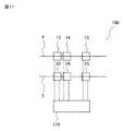
- FIG. 11 is a diagram showing a configuration of an optical waveguide device according to the fourth embodiment of the present invention.
- the optical waveguide device 100 includes a first optical waveguide 4, a second optical waveguide 5, and a control circuit 110.
- the first optical waveguide 4 and the second optical waveguide 5 include electrodes 13 to 15 and electrodes 23 to 25, respectively.
- the electrode 15 and the electrode 25 output a light absorption current corresponding to the intensity of light transmitted through the first optical waveguide 4 and the second optical waveguide 5.
- the control circuit 110 controls the first loss change and the first phase change that occur in the light transmitted through the first optical waveguide 4 by the voltage applied to the electrodes 13 and 14. Further, the control circuit 110 controls the second loss change and the second phase change that occur in the light transmitted through the second optical waveguide 5 by the voltage applied to the electrodes 13 and 14. Then, the control circuit 110 controls the voltage applied to the electrodes 13, 14, 23, and 24 so that the first phase change and the second phase change have a predetermined relationship. Alternatively, the control circuit 110 controls the voltage applied to the electrodes 13, 14, 23, and 24 so that the first loss change and the second loss change have a predetermined relationship.
- the optical waveguide device 100 keeps the phase difference of light transmitted through the first optical waveguide 4 and the second optical waveguide 5 constant according to the procedure described in the first embodiment. It is possible to control the loss of the first optical waveguide 4 and the second optical waveguide 5 without change.
- the optical waveguide device 100 is configured so that the loss of light transmitted through the first optical waveguide 4 and the second optical waveguide 5 is kept constant by the procedure described in the third embodiment. It is also possible to control the phase difference generated between 4 and the second optical waveguide 5.
- control circuit 110 compares the light absorption current output from the electrode 15 and the electrode 25, calculates a voltage value to be applied to the electrodes 13, 14, 23, and 24 based on the result, and calculates the voltage to the electrode 13, 14, 23 and 24 may be output. That is, in the optical waveguide device 100 as well, it is possible to detect the intensity of light transmitted through the first optical waveguide 4 and the second optical waveguide 5 based on the light absorption current, as in the first embodiment. is there. Then, based on the detected light intensity, the first optical waveguide 4 and the second optical waveguide are set such that the intensity of the light transmitted through the first optical waveguide 4 and the second optical waveguide 5 has a predetermined relationship. The loss of the waveguide 5 may be controlled.
- the optical waveguide device 100 may include only the first optical waveguide 4 and the control circuit 110.
- the first optical waveguide 4 may include only the electrodes 13 and 14.
- the control circuit 110 calculates a voltage value to be applied to the electrodes 13 and 14 so as to cause a predetermined phase change and loss change in the first optical waveguide 4 and outputs a signal of the voltage to the electrodes 13 and 14. To do.
- the loss and phase of the first optical waveguide 4 can be controlled by the voltage output to the electrodes 13 and 14. .
- the loss of the first optical waveguide 4 is controlled with the phase change of the light transmitted through the first optical waveguide 4 kept constant by the procedure described in FIGS. 5 to 7 of the first embodiment. Is possible.
- the modification of the fourth embodiment also has an effect that the phase difference and loss of light transmitted through the optical waveguide device can be independently controlled with a simple configuration.
- An optical waveguide comprising two electrodes to which two signals are respectively applied; Control means for controlling the two signals so that a phase change and a loss change generated in the light transmitted through the optical waveguide by the two signals have a predetermined value;
- An optical waveguide device comprising: (Appendix 2) A monitor means for outputting a monitor signal corresponding to the intensity of the light transmitted through the optical waveguide; The optical waveguide device according to appendix 1, wherein the control unit further controls the two signals based on the monitor signal.
- a first optical waveguide comprising a first electrode and a second electrode to which a first signal and a second signal for controlling the phase and loss of the input first light are respectively applied;
- a second optical waveguide comprising a fourth electrode and a fifth electrode to which a fourth signal and a fifth signal for controlling the phase and loss of the input second light are respectively applied;
- Control means for generating the first, second, fourth and fifth signals so that any one of the second phase changes generated in the light has a predetermined relationship
- An optical waveguide device comprising: (Appendix 4)
- the control means includes the first and second loss changes so that any one of the first loss change and the second loss change and the first phase change and the second phase change are equal. 2.
- the optical waveguide device according to appendix 3 which generates the second, fourth and fifth signals.
- Monitor means for outputting a third signal and a sixth signal respectively corresponding to the intensities of the light transmitted through the first and second optical waveguides;
- the optical waveguide device according to any one of appendix 3 or 4, wherein the control unit controls the first and second loss changes based on the third signal and the sixth signal.
- Appendix 6 The optical waveguide device according to appendix 5, wherein the control unit controls the first and second loss changes so that the intensities of the light transmitted through the first and second optical waveguides are equal to each other.
- the first and second monitoring means absorb the light transmitted through the first and second optical waveguides to generate the third and sixth signals, respectively.
- the optical waveguide device each comprising: (Appendix 8)
- the control means includes First storage means for storing first characteristic data indicating a relationship between a voltage change of the first signal and a voltage of the second signal and a phase change and a loss change of light transmitted through the first optical waveguide.
- Second storage means for storing second characteristic data indicating the relationship between the voltage of the fourth signal and the voltage of the fifth signal and the phase change and loss change of the light transmitted through the second optical waveguide.
- Computing means for calculating respective voltages of the first, second, fourth and fifth signals,
- the optical waveguide device according to any one of appendices 3 to 7.
- Branching means for branching input light into first light and second light;
- Coupling means for coupling and outputting light output from the optical waveguide device;
- An optical interferometer An optical interferometer.
- a first optical waveguide comprising a first electrode and a second electrode to which a first signal and a second signal are applied, respectively, and a fourth electrode to which a fourth signal and a fifth signal are applied, respectively
- an optical waveguide device comprising: a second optical waveguide comprising a fifth electrode; The first loss change caused in the light transmitted through the first optical waveguide by the first and second signals and the second loss generated in the light transmitted through the second optical waveguide by the fourth and fifth signals.
- Loss change, first phase change caused in light transmitted through the first optical waveguide by the first and second signals, and transmission through the second optical waveguide by the fourth and fifth signals Outputting the first, second, fourth, and fifth signals so that any one of the second phase changes generated in the light has a predetermined relationship;
- Control circuit for optical waveguide devices Appendix 11
- An input optical waveguide for inputting input light, a first optical interferometer, a second optical interferometer, and the input light are branched to the first optical interferometer and the second optical interferometer.
- Each of the first optical interferometer and the second optical interferometer further includes two optical waveguides arranged in parallel and the optical waveguide device described in any one of appendices 1 to 4,
- the first optical waveguide and the second optical waveguide of the optical waveguide device provided in the first optical interferometer and the second optical interferometer are in series with the two optical waveguides arranged in parallel, respectively. It is connected, The optical interferometer described in Appendix 12.
Landscapes
- Physics & Mathematics (AREA)
- Nonlinear Science (AREA)
- Optics & Photonics (AREA)
- General Physics & Mathematics (AREA)
- Electromagnetism (AREA)
- Engineering & Computer Science (AREA)
- Computer Networks & Wireless Communication (AREA)
- Signal Processing (AREA)
- Optical Modulation, Optical Deflection, Nonlinear Optics, Optical Demodulation, Optical Logic Elements (AREA)
Abstract
Priority Applications (1)
| Application Number | Priority Date | Filing Date | Title |
|---|---|---|---|
| US14/122,768 US9069193B2 (en) | 2011-06-01 | 2012-05-31 | Optical waveguide device, optical interferometer, and method for producing optical waveguide device |
Applications Claiming Priority (2)
| Application Number | Priority Date | Filing Date | Title |
|---|---|---|---|
| JP2011-123204 | 2011-06-01 | ||
| JP2011123204 | 2011-06-01 |
Publications (1)
| Publication Number | Publication Date |
|---|---|
| WO2012165656A1 true WO2012165656A1 (fr) | 2012-12-06 |
Family
ID=47259496
Family Applications (1)
| Application Number | Title | Priority Date | Filing Date |
|---|---|---|---|
| PCT/JP2012/064608 Ceased WO2012165656A1 (fr) | 2011-06-01 | 2012-05-31 | Dispositif de guide d'onde optique, interféromètre optique, et procédé de production de dispositif de guide d'onde optique |
Country Status (3)
| Country | Link |
|---|---|
| US (1) | US9069193B2 (fr) |
| JP (1) | JPWO2012165656A1 (fr) |
| WO (1) | WO2012165656A1 (fr) |
Cited By (8)
| Publication number | Priority date | Publication date | Assignee | Title |
|---|---|---|---|---|
| JP2012255929A (ja) * | 2011-06-09 | 2012-12-27 | Mitsubishi Electric Corp | 光変調器および光変調方法 |
| JP2015184506A (ja) * | 2014-03-25 | 2015-10-22 | 日本電気株式会社 | 光送受信器 |
| JP2015219500A (ja) * | 2014-05-21 | 2015-12-07 | 日本電信電話株式会社 | マッハツェンダ型光変調器、光iq変調器、およびその制御方法 |
| JP2016522450A (ja) * | 2013-06-12 | 2016-07-28 | メドルミクス, エセ.エレ.Medlumics, S.L. | ゼロの残留振幅変調を有している、電気光学シリコンに基づく位相変調装置 |
| JP2017211607A (ja) * | 2016-05-27 | 2017-11-30 | 日本電信電話株式会社 | 光変調器 |
| JP2018004979A (ja) * | 2016-07-04 | 2018-01-11 | 日本電気株式会社 | 光変調装置および光変調方法 |
| WO2021234911A1 (fr) * | 2020-05-21 | 2021-11-25 | 三菱電機株式会社 | Modulateur de phase optique |
| JP2024543788A (ja) * | 2021-02-07 | 2024-11-26 | ニューフォトニクス リミテッド | 集積フォトニック・システムの較正、監視及び制御のためのデバイス及び方法 |
Families Citing this family (12)
| Publication number | Priority date | Publication date | Assignee | Title |
|---|---|---|---|---|
| JPWO2012073447A1 (ja) * | 2010-12-01 | 2014-05-19 | 日本電気株式会社 | 光強度減算器、光a/d変換器及び光強度減算方法 |
| EP2843462A4 (fr) * | 2012-04-27 | 2015-12-30 | Nec Corp | Modulateur optique de type mach-zehnder, système émetteur/récepteur optique et procédé de commande de modulateur optique de type mach-zehnder |
| US20160036532A1 (en) * | 2013-03-15 | 2016-02-04 | Nec Corporation | Optical modulator, optical transmitter, optical transmission/reception system, and control method for optical modulator |
| US9571313B2 (en) * | 2014-09-12 | 2017-02-14 | Mer-Cello Wireless Solutions Ltd. | Full-optical multiwavelet orthogonal frequency divisional multiplexing (OFDM) and demultiplexing |
| US10084619B2 (en) | 2016-06-03 | 2018-09-25 | International Business Machines Corporation | Nested feed-forward optical equalization using an electro-optic modulator with a multi-segment electrode |
| US10120210B2 (en) * | 2016-06-03 | 2018-11-06 | International Business Machines Corporation | Feed-forward optical equalization using an electro-optic modulator with a multi-segment electrode and distributed drivers |
| US10168596B2 (en) | 2017-05-23 | 2019-01-01 | Elenion Technoogies, LLC | Optical waveguide modulator |
| US10466567B1 (en) | 2018-04-24 | 2019-11-05 | Elenion Technologies, Llc | Optical waveguide modulator |
| JP7600724B2 (ja) * | 2021-01-28 | 2024-12-17 | 住友電気工業株式会社 | 光変調器の製造方法、試験方法、および試験プログラム、ならびに光送信装置 |
| JP7608867B2 (ja) * | 2021-02-26 | 2025-01-07 | 富士通株式会社 | 光変調器、光送信器及び光通信装置 |
| WO2022225543A1 (fr) * | 2021-04-22 | 2022-10-27 | Futurewei Technologies, Inc. | Conception d'électrode d'un modulateur opto-électrique localisé |
| CN117355790B (zh) * | 2021-05-25 | 2026-07-03 | 三菱电机株式会社 | 半导体光相位调制器及其检查方法 |
Citations (2)
| Publication number | Priority date | Publication date | Assignee | Title |
|---|---|---|---|---|
| JPH0749473A (ja) * | 1993-08-05 | 1995-02-21 | Hitachi Ltd | マッハツェンダ型変調器 |
| JP2011247926A (ja) * | 2010-05-24 | 2011-12-08 | Fujitsu Ltd | マッハツェンダ型変調器の制御方法及び光モジュール |
Family Cites Families (12)
| Publication number | Priority date | Publication date | Assignee | Title |
|---|---|---|---|---|
| US5137359A (en) * | 1991-03-18 | 1992-08-11 | Litton Systems, Inc. | Digital phase modulator for fiber optic sagnac interferometer |
| JP3742477B2 (ja) | 1997-02-17 | 2006-02-01 | 富士通株式会社 | 光変調器 |
| JP2001209018A (ja) | 2000-01-26 | 2001-08-03 | Nec Corp | モニタ付き光変調器 |
| JP3974792B2 (ja) | 2002-02-07 | 2007-09-12 | 富士通株式会社 | 光導波路デバイス及び光デバイス |
| JP4922594B2 (ja) * | 2005-05-23 | 2012-04-25 | 富士通株式会社 | 光送信装置、光受信装置、およびそれらを含む光通信システム |
| JP4696264B2 (ja) | 2005-08-24 | 2011-06-08 | 独立行政法人情報通信研究機構 | 強度バランス機能を有する光fsk/ssb変調器 |
| JP4422661B2 (ja) * | 2005-08-31 | 2010-02-24 | 富士通株式会社 | 差動4位相偏移変調器の駆動電圧設定方法 |
| WO2008048434A2 (fr) * | 2006-10-07 | 2008-04-24 | Sioptical, Inc. | Modulateur optique segmenté |
| EP2896993B1 (fr) * | 2007-06-13 | 2019-04-24 | Ramot at Tel Aviv University Ltd. | Système et procédé de conversion de données numériques en un signal optique analogique modulé en intensité |
| JP5198996B2 (ja) | 2008-09-19 | 2013-05-15 | 住友大阪セメント株式会社 | 光変調器 |
| US8320720B2 (en) * | 2009-08-19 | 2012-11-27 | Mark Webster | Advanced modulation formats for silicon-based optical modulators |
| US9158175B2 (en) * | 2010-01-27 | 2015-10-13 | K G Technology Associates, Inc. | Optical coupler |
-
2012
- 2012-05-31 WO PCT/JP2012/064608 patent/WO2012165656A1/fr not_active Ceased
- 2012-05-31 US US14/122,768 patent/US9069193B2/en active Active
- 2012-05-31 JP JP2013518197A patent/JPWO2012165656A1/ja active Pending
Patent Citations (2)
| Publication number | Priority date | Publication date | Assignee | Title |
|---|---|---|---|---|
| JPH0749473A (ja) * | 1993-08-05 | 1995-02-21 | Hitachi Ltd | マッハツェンダ型変調器 |
| JP2011247926A (ja) * | 2010-05-24 | 2011-12-08 | Fujitsu Ltd | マッハツェンダ型変調器の制御方法及び光モジュール |
Cited By (11)
| Publication number | Priority date | Publication date | Assignee | Title |
|---|---|---|---|---|
| JP2012255929A (ja) * | 2011-06-09 | 2012-12-27 | Mitsubishi Electric Corp | 光変調器および光変調方法 |
| JP2016522450A (ja) * | 2013-06-12 | 2016-07-28 | メドルミクス, エセ.エレ.Medlumics, S.L. | ゼロの残留振幅変調を有している、電気光学シリコンに基づく位相変調装置 |
| JP2015184506A (ja) * | 2014-03-25 | 2015-10-22 | 日本電気株式会社 | 光送受信器 |
| US10749601B2 (en) | 2014-03-25 | 2020-08-18 | Nec Corporation | Optical transceiver |
| JP2015219500A (ja) * | 2014-05-21 | 2015-12-07 | 日本電信電話株式会社 | マッハツェンダ型光変調器、光iq変調器、およびその制御方法 |
| JP2017211607A (ja) * | 2016-05-27 | 2017-11-30 | 日本電信電話株式会社 | 光変調器 |
| JP2018004979A (ja) * | 2016-07-04 | 2018-01-11 | 日本電気株式会社 | 光変調装置および光変調方法 |
| WO2021234911A1 (fr) * | 2020-05-21 | 2021-11-25 | 三菱電機株式会社 | Modulateur de phase optique |
| JPWO2021234911A1 (fr) * | 2020-05-21 | 2021-11-25 | ||
| JP2024543788A (ja) * | 2021-02-07 | 2024-11-26 | ニューフォトニクス リミテッド | 集積フォトニック・システムの較正、監視及び制御のためのデバイス及び方法 |
| JP7828110B2 (ja) | 2021-02-07 | 2026-03-11 | ニューフォトニクス リミテッド | 集積フォトニック・システムの較正、監視及び制御のためのデバイス及び方法 |
Also Published As
| Publication number | Publication date |
|---|---|
| US20140099053A1 (en) | 2014-04-10 |
| JPWO2012165656A1 (ja) | 2015-02-23 |
| US9069193B2 (en) | 2015-06-30 |
Similar Documents
| Publication | Publication Date | Title |
|---|---|---|
| JPWO2012165656A1 (ja) | 光導波路デバイス、光干渉計及び光導波路デバイスの制御方法 | |
| Samani et al. | A silicon photonic PAM-4 modulator based on dual-parallel Mach–Zehnder interferometers | |
| US9874800B2 (en) | MZM linear driver for silicon photonics device characterized as two-channel wavelength combiner and locker | |
| US8280201B2 (en) | Traveling wave Mach-Zehnder optical device | |
| US6650458B1 (en) | Electro-optic modulator with continuously adjustable chirp | |
| US7907324B2 (en) | Optical modulator and controlling method and apparatus thereof | |
| JP5550825B2 (ja) | モニタリング構造を備えた光位相変調器 | |
| US9240838B2 (en) | Optical transmitter and method for controlling bias for optical modulator | |
| US7911675B2 (en) | Optical modulation device and optical semiconductor device | |
| CN109643030B (zh) | 光学调制器及使用方法 | |
| US10901153B2 (en) | Null bias mach-zehnder interferometer with ring resonators | |
| US20160127070A1 (en) | Integrated two-channel spectral combiner and wavelength locker in silicon photonics | |
| US10191306B2 (en) | Dither free bias control | |
| WO2011043079A1 (fr) | Module de modulation optique et procédé de modulation d'un signal optique | |
| US20150063742A1 (en) | Method for modulating a carrier light wave | |
| JP2012155238A (ja) | 光変調器 | |
| US9223184B2 (en) | Optical modulator | |
| US12001115B2 (en) | Optical modulator and method of use | |
| US11194219B2 (en) | Optical modulator | |
| JP6306939B2 (ja) | マッハツェンダ型光変調器の制御方法 | |
| JP2010072462A (ja) | 光変調器 | |
| US9547214B2 (en) | Device for transmitting and/or modulating optical signals with passive phase shifters | |
| US9298024B2 (en) | Semiconductor Mach-Zender modulator and method to drive the same | |
| JP2013174761A (ja) | 光送信器、光通信システムおよび光送信方法 | |
| US11194220B2 (en) | Calibrating and controlling nested Mach-Zehnder interferometer that includes pre-stages |
Legal Events
| Date | Code | Title | Description |
|---|---|---|---|
| 121 | Ep: the epo has been informed by wipo that ep was designated in this application |
Ref document number: 12792036 Country of ref document: EP Kind code of ref document: A1 |
|
| ENP | Entry into the national phase |
Ref document number: 2013518197 Country of ref document: JP Kind code of ref document: A |
|
| WWE | Wipo information: entry into national phase |
Ref document number: 14122768 Country of ref document: US |
|
| NENP | Non-entry into the national phase |
Ref country code: DE |
|
| 122 | Ep: pct application non-entry in european phase |
Ref document number: 12792036 Country of ref document: EP Kind code of ref document: A1 |