WO2012172708A1 - Dispositif de sauvegarde et procédé de fonctionnement du dispositif de sauvegarde - Google Patents
Dispositif de sauvegarde et procédé de fonctionnement du dispositif de sauvegarde Download PDFInfo
- Publication number
- WO2012172708A1 WO2012172708A1 PCT/JP2011/078511 JP2011078511W WO2012172708A1 WO 2012172708 A1 WO2012172708 A1 WO 2012172708A1 JP 2011078511 W JP2011078511 W JP 2011078511W WO 2012172708 A1 WO2012172708 A1 WO 2012172708A1
- Authority
- WO
- WIPO (PCT)
- Prior art keywords
- memory
- work memory
- log data
- storage
- backup device
- Prior art date
- Legal status (The legal status is an assumption and is not a legal conclusion. Google has not performed a legal analysis and makes no representation as to the accuracy of the status listed.)
- Ceased
Links
Images



Classifications
-
- G—PHYSICS
- G06—COMPUTING OR CALCULATING; COUNTING
- G06F—ELECTRIC DIGITAL DATA PROCESSING
- G06F11/00—Error detection; Error correction; Monitoring
- G06F11/07—Responding to the occurrence of a fault, e.g. fault tolerance
- G06F11/14—Error detection or correction of the data by redundancy in operations
- G06F11/1446—Point-in-time backing up or restoration of persistent data
- G06F11/1456—Hardware arrangements for backup
Definitions
- the present invention relates to a backup device that backs up log data created by a computer and an operation method of the backup device.
- an uninterruptible power supply is sometimes attached to a computer in order to operate the computer safely (JP 2009-3789, FIG. 2 (Patent Document 1)).
- the computer is supplied with power from a commercial power source, and the UPS is supplied with power for charging from the commercial power source.
- power loss When a power failure occurs in a commercial power supply (hereinafter referred to as “power loss”), log data created by a computer can be safely and reliably stored by supplying electricity from a battery built into the UPS as a power source for the computer. Can be saved.
- the UPS when the UPS is provided, the log data can be stored safely and reliably.
- the UPS since the UPS is generally large, it is difficult to secure an installation space and the cost of the UPS is high.
- the log data to be backed up created by the computer has a small capacity (for example, 4 MB or less), the log data can be saved at a small size and at a low cost by using, for example, a battery-backed SRAM.
- a battery-backed SRAM has a relatively small storage capacity. For this reason, in the method using only the SRAM, when the log data to be backed up has a large capacity (several tens of MB), the number of SRAM (the number of parts) increases to increase the size and cost.
- an object of the present invention is to provide a backup device that can store a large amount of log data safely and reliably, and can be realized in a small size and at a low cost.
- the backup device of the present invention provides: Work memory consisting of SRAM that can be battery-backed stored data, A storage memory composed of a non-volatile memory having a higher recording density than the work memory; An interface unit interposed between the host computer and the work memory and the storage memory, and allowing the host computer to access the work memory and the storage memory; And a control unit that performs control to transfer and store the log data transferred from the host computer to the work memory via the interface unit and stored in the storage memory.
- the backup device of the present invention stores a large amount of log data as follows.
- the host computer transfers a part of a large amount of log data to the work memory via the interface unit.
- the control unit controls the work memory, and transfers and stores the part of the log data to the storage memory.
- the control unit transfers and stores another part of the log data to the storage memory.
- the control unit sequentially transfers a part of the log data to the storage memory and stores it. Since the work memory is composed of SRAM, the log data can be stored in the work memory at a relatively high speed. On the other hand, since the storage memory has a higher recording density than the work memory, a larger amount of log data can be stored in the storage memory.
- the work memory is composed of SRAM which can be backed up by a battery
- the storage memory is composed of nonvolatile memory. Therefore, even if the power is cut off, the log data can be kept in the work memory or the storage memory. For this reason, a large amount of the log data can be stored safely and reliably.
- this backup device can be realized with a relatively small size and low cost by using commercially available parts, and space and UPS costs can be omitted as compared with the case where a UPS is provided.
- the storage memory is omitted and the log data is backed up only with the work memory made of SRAM, the number of SRAMs (number of parts) increases, resulting in an increase in size and cost.
- the storage memory composed of the nonvolatile memory has a relatively slow operation speed, so the log data is stored in the storage memory. The speed is slow.
- a power-off detector that detects that a power-off has occurred; When the power-off detection unit detects the power-off, a cutoff control unit that performs control to cut off access to the work memory and the storage memory; When returning from the power-off, a part of the log data stored in the work memory is transferred to the storage memory when the power-off occurs, and another part of the log data remains.
- a transfer state detection unit that detects whether or not it was in the middle, When the transfer state detection unit detects that the transfer state is in the middle of the transfer when the power interruption occurs, the control unit detects the other log data that remains untransferred in the work memory. Control is performed to transfer the portion to the storage memory and store it.
- the power interruption detection unit detects the power interruption. Then, the blocking control unit performs control to block access to the storage memory.
- the power interruption occurs, if the log data stored in the work memory is in the process of being transferred to the storage memory, the part of the log data is transferred to the storage memory, and The other part of the log data remains untransferred in the work memory (this is referred to as a “transfer-in-progress state”).
- the transfer state detection unit detects whether the transfer is in progress.
- the control unit detects that the transfer state detection unit is in the middle of the transfer, the control unit stores the other part of the log data remaining untransferred in the work memory.
- the backup device includes a contention control unit that arbitrates contention between access to the work memory and access to the storage memory.
- the host computer and the control unit arbitrate contention between access to the work memory by the host computer and the control unit and access to the storage memory. , Each of the work memory and the storage memory can be accessed smoothly.
- the interface unit includes a local bridge, and the local bridge is provided between the data bus of the host computer and the control unit, the work memory, and the storage memory. It is connected to a data bus.
- the data bus of the host computer and the data bus provided between the control unit, the work memory, and the storage memory are connected by the local bridge. Therefore, the host computer can directly access the work memory and the storage memory.
- the backup device includes a board that can be attached to and detached from the motherboard of the host computer, and the work memory, the storage memory, the interface unit, and the control unit are mounted on the board. It is characterized by being.
- the work memory, the storage memory, the interface unit, and the control unit are mounted on the substrate. Therefore, a one-board (substrate) type backup device separate from the mother board is configured. Such a one-board type backup device can be easily installed and applied to an existing host computer without requiring a design change of the motherboard.
- the work memory, the storage memory, the interface unit, and the control unit are mounted on a motherboard of the host computer.
- the configuration of the backup device as well as the motherboard is reduced in size as a whole. can do.
- the work memory can be written at a transfer rate of the log data transferred from the host computer.
- the log data can be written into the work memory at a speed at which the log data is transferred from the host computer, the log data is saved from the work memory. Can be smoothly transferred to and stored in the memory.
- the work memory includes two physically independent SRAMs.
- the work memory is composed of two physically independent SRAMs, hardware restrictions can be reduced and the degree of design freedom can be increased. it can.
- the backup device is characterized in that the storage memory is a NOR flash memory.
- the storage memory is composed of a NOR flash memory, unlike the NAND system, the configuration of the file management area or the like is not destroyed at the time of power interruption. Therefore, the log data can be stored more safely and reliably.
- the control unit transfers a part of the log data stored in the work memory to the storage memory in units of storage capacity of the work memory and stores it. And a second process of transferring and storing another part of the log data remaining untransferred in the work memory to the storage memory in units of storage capacity of the work memory. These processes are performed at least sequentially.
- the process of transferring a part of the log data stored in the work memory to the storage memory in units of the storage capacity of the work memory is stored. Since the process is repeated, the log data can be efficiently transferred from the work memory to the storage memory and stored.
- the backup device of this invention A work memory made of FeRAM; A storage memory composed of a non-volatile memory having a higher recording density than the work memory; An interface unit interposed between the host computer and the work memory and the storage memory, and allowing the host computer to access the work memory and the storage memory; And a control unit that performs control to transfer and store the log data transferred from the host computer to the work memory via the interface unit and stored in the storage memory.
- the backup device of the present invention stores a large amount of log data as follows.
- the host computer transfers a part of a large amount of log data to the work memory via the interface unit.
- the control unit controls the work memory, and transfers and stores the part of the log data to the storage memory.
- the control unit transfers and stores another part of the log data to the storage memory.
- the control unit sequentially transfers a part of the log data to the storage memory and stores it. Since the work memory is composed of FeRAM (Ferroelectric Random Access Memory), the control unit can store the log data in the work memory at a relatively high speed. On the other hand, since the storage memory has a higher recording density than the work memory, the control unit can store a larger amount of log data in the storage memory.
- the work memory is composed of FeRAM which is a nonvolatile memory
- the storage memory is composed of a nonvolatile memory. Therefore, even if the power is cut off, the log data can be kept in the work memory or the storage memory. For this reason, a large amount of the log data can be stored safely and reliably.
- this backup device can be realized with a relatively small size and low cost by using commercially available parts, and space and UPS costs can be omitted as compared with the case where a UPS is provided.
- the storage memory is omitted and the log data is backed up only by the work memory made of FeRAM, the number of FeRAMs (number of parts) increases, resulting in an increase in size and cost.
- the storage memory consisting of non-volatile memory has a relatively slow operating speed. The storage speed is slow.
- a large-capacity log data can be stored safely and reliably, and a backup device that can be realized in a small size and at a low cost can be realized.
- the log data stored in the work memory is repeatedly transferred to the storage memory and stored in units of the storage capacity of the work memory. Data can be efficiently transferred from the work memory to the storage memory for storage.
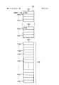
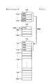
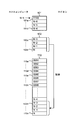
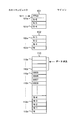
- FIG. 1 It is a figure which shows the aspect by which the backup apparatus of one Embodiment of this invention was connected to the host computer. It is a figure which shows the initial state before storing log data about the work memory and the preservation
- FIG. 1 shows a state in which a backup device 1 according to an embodiment of the present invention is connected to a host computer 2.
- the backup device 1 includes one substrate 1A. On the substrate 1A, a work memory 100, a storage memory 110, an FPGA (Field-Programmable Gate Array) 120 as an interface unit, and a microcomputer (hereinafter abbreviated as “microcomputer”) 130 as a control unit. First to fourth buffers 141, 142, 143, and 144, a battery 150 for backing up the work memory 100, a power-off detector 190, an address bus 161 for designating an address, and data A data bus 162 for transferring and a control signal bus 163 for controlling access are mounted.
- the FPGA 120 includes a contention control unit 121 and a local bridge 122.
- the backup device 1 is connected to a host computer 2.
- the board 1A of the backup device 1 is detachably attached to a motherboard 2A of the host computer 2 via a PCI (Peripheral Component Component) slot (not shown). Therefore, such a one-board type backup device 1 can be easily applied to an existing host computer without requiring a design change of the motherboard of the host computer.
- PCI Peripheral Component Component
- the work memory 100 includes a first work memory 101 composed of one SRAM having a storage capacity of 4 MB and a first SRAM composed of one SRAM having a storage capacity of 4 MB. It consists of two parts in total, with two work memories 102. Since the work memory 100 is composed of SRAM, the log data can be stored in the work memory 100 at a relatively high speed. In addition, since the work memory 100 is divided into two SRAMs, hardware restrictions can be reduced and design flexibility can be increased.
- the memory cells of the first work memory 101 and the second work memory 102 are accessed by specifying addresses.
- the storage areas of the first work memory 101 and the second work memory 102 are divided into four 1 MB storage areas 101a to 101d and 102a to 102d.
- first and second work memories 101 and 102 are backed up by a battery 150 in FIG.
- the work memory 100 is connected to the contention control unit 121 and the local bridge 122 of the FPGA 120 via the address bus 161 and the second buffer 142, while the local address bus 162 and the fourth buffer Are connected to the competition control unit 121 and the microcomputer 130 through the buffer 144.
- the work memory 100 is connected to the local bridge 122 via the data bus 163 and the second buffer 142, and is connected to the microcomputer 130 via the local data bus 164 and the fourth buffer 144. ing. Further, the work memory 100 is connected to the contention control unit 121 via the memory control signal bus 171.
- the storage memory 110 is composed of a NOR flash memory which is a nonvolatile memory having a higher recording density than the work memory 100. Since the storage memory 110 has a higher recording density than the work memory 100, a larger amount of log data can be stored in the storage memory 110. Further, unlike the NAND flash memory, the storage memory 110 does not destroy the configuration of the file management area or the like when the power is interrupted. Therefore, log data can be stored more safely and reliably.
- the work memory 100 is composed of an SRAM that can be backed up by a battery, and the storage memory 110 is composed of a nonvolatile memory. Therefore, even if the power is cut off, the log data can be kept in the work memory 100 or the storage memory 110. For this reason, a large amount of the log data can be stored safely and reliably.
- Each memory cell of the storage memory 110 is accessed by designating an address in the same manner as the first work memory 101 and the second work memory 102.
- the storage area of the storage memory 110 is divided into N storage areas 110a to 110n each having 1 MB.
- N 64, that is, the storage memory 110 has a storage capacity of 64 MB.
- the storage memory 110 is connected to the contention control unit 121 and the local bridge 122 of the FPGA 120 via the address bus 161 and the first buffer 141, similarly to the work memory 100.
- the contention controller 121 and the microcomputer 130 are connected via the local address bus 162 and the third buffer 143.
- the storage memory 110 is connected to the local bridge 122 via the data bus 163 and the first buffer 141, and is connected to the microcomputer 130 via the local data bus 164 and the third buffer 143. Yes. Further, the storage memory 110 is connected to the contention control unit 121 via the memory control signal bus 171.
- the local bridge 122 is connected to the contention control unit 121 via an address bus 161 and a main memory control signal bus 172, while being connected via a PCI bus or a PCI express (registered trademark, hereinafter referred to as PCIe) bus 210. It is connected to a chip set 205 of the host computer 2 described later.
- the local bridge 122 converts the data from the host computer 2 into log data, address information where the log data is to be stored, and an access request to the work memory 100 or the storage memory 110, respectively.
- the local bridge 122 transfers log data to the second buffer 142 via the data bus 163 and transfers address information where the log data is to be stored to the second buffer 142 via the address bus 161. To do.
- the local bridge 122 transfers address information in which log data is to be stored to the contention control unit 121 via the address bus 161, and controls access to the work memory 100 or the storage memory 110 as main memory control. Transfer to the competition control unit 121 via the signal bus 172. Therefore, the host computer 2 can directly access the work memory 100 and the storage memory 110.
- the contention control unit 121 receives the address information where the log data is to be stored and the access request to the work memory 100 or the storage memory 110 from the local bridge 122.
- the contention control unit 121 is connected to the microcomputer 130 via a local address bus 162 and a local memory control signal bus 173. Then, the contention control unit 121 receives from the microcomputer 130 address information where log data should be stored and an access request to the work memory 100 or the storage memory 110.
- the contention control unit 121 is connected to the first and second buffers 141 and 142 via the main buffer control signal bus 174, while the third and fourth buffers are connected via the local buffer control line 175. It is connected to the buffers 143 and 144.
- the contention control unit 121 receives the first to first data based on data received from the local bridge 122 and the microcomputer 130 (address information in which log data is to be stored and access request signals to the work memory 100 or the storage memory 110).
- the fourth buffers 141, 142, 143, and 144 are controlled. Specifically, the contention control unit 121 receives a request for access from the host computer 2 to the work memory 100 or the storage memory 110 and a request from the microcomputer 130 to access the work memory 100 or the storage memory 110. Mediate conflicts.
- the contention control unit 121 permits only one of the host computer 2 and the microcomputer 130 to access the work memory 100 or the storage memory 110 and does not permit access to the other. Therefore, the host computer 2 and the microcomputer 130 can smoothly access the work memory 100 and the storage memory 110, respectively.
- the microcomputer 130 controls the work memory 100 to transfer a part of the log data stored in the work memory 100 to the storage memory 110 for storage. Next, the microcomputer 130 transfers another part of the log data to the storage memory 110 and stores it. In addition, the microcomputer 130 controls the operation of the entire backup device 1.
- the power-off detection unit 190 is connected to the power supply box 3 via the host computer 2 and is connected to the FPGA 120 and the microcomputer 130.
- the power-off detection unit 190 detects the occurrence of power-off of the power supply box 3 based on voltage, and transmits a power-off occurrence signal to the CPU 201 of the host computer 2, the competition control unit 121 of the FPGA 120, and the microcomputer 130. .
- the power-off detection unit 190 may be mounted not on the board 1A of the backup device 1 but on the motherboard 2A of the host computer 2.
- the host computer 2 includes a CPU 201, a main memory 202, a hard disk (not shown), a CF card 203 as a removable disk, a BIOS (Basic Input / Output System), a flash ROM 204, and a chip set. 205 and an internal power conversion unit 206.
- the CPU 201 is connected to the main memory 202 and the chip set 205 via a bus on the mother board 2A.
- the chip set 205 is connected to the CF card 203 and the BIOS / flash / ROM 204 via the bus, and to the local bridge 122 of the backup device 1 via the PCI bus or the PCIe bus 210 as described above. Has been.
- While the internal power conversion unit 206 is connected to the power supply box 3, as shown in FIG. 1, the work memory 100, the storage memory 110, the FPGA 120, the microcomputer 130, the first memory of the backup device 1 Through the fourth buffer 141, 142, 143, 144, the CPU 201 of the host computer 2, the main memory 202, the hard disk and CF card 203, the BIOS / flash ROM 204, and the chip set 205.
- the internal power conversion unit 206 converts the AC power of the power supply box 3 into a DC power and supplies it to each element connected to the backup device 1 and the host computer 2.
- the backup device 1 operates in general with the host computer 2 as follows.
- Log data is transferred from the CPU 201 to the local bridge 122 via the chip set 205 under the control of the CPU 201. Then, the log data is converted by the local bridge 122, and address information in which the log data is to be stored and a signal for requesting access to the work memory 100 are transferred to the contention control unit 121.
- the contention control unit 121 Upon receiving the address information where the log data should be stored and the signal requesting access to the work memory 100 from the CPU 201, the contention control unit 121 requests access from the microcomputer 130 to the work memory 100 or the storage memory 110. Determine if there is any.
- the contention control unit 121 controls the second buffer 142 to allow the CPU 201 to access the work memory 100.
- the contention control unit 121 performs contention control and controls the second buffer 142 immediately or after a predetermined time has elapsed.
- the CPU 201 permits access to the work memory 100 from the CPU 201.
- the log data and the address information where the log data is to be stored are transferred from the local bridge 122 to the work memory 100, and the log data is stored at a predetermined address in the work memory 100.
- the speed at which the log data is stored in the work memory 100 that is, the writing speed is relatively high, and is substantially the same as the transfer speed of the log data from the CPU 201 to the work memory 100. Therefore, the log data can be smoothly transferred from the work memory 100 to the storage memory 110 and stored.
- the address information where the log data should be stored and the work memory 100 are stored.
- a signal requesting access is transmitted from the microcomputer 130 to the contention control unit 121.
- the contention control unit 121 Upon receiving the address information where the log data is to be stored and the signal requesting access to the work memory 100 from the microcomputer 130, the contention control unit 121 requests access from the CPU 201 to the work memory 100 or the storage memory 110. Determine if there is any.
- the contention control unit 121 controls the fourth buffer 144 to permit the microcomputer 130 to access the work memory 100.
- the contention control unit 121 performs contention control and controls the fourth buffer 144 immediately or after a predetermined time has elapsed. Access from the microcomputer 130 to the work memory 100 is permitted. Then, the microcomputer 130 transfers address information in which log data is to be stored in the work memory 100 and reads predetermined log data from the work memory 100.
- the contention control unit 121 For the predetermined log data, under the control of the microcomputer 130, address information where the log data is to be stored and a signal requesting access to the storage memory 110 are transmitted from the microcomputer 130 to the contention control unit 121. Upon receiving the address information where the predetermined log data is to be stored and a signal requesting access to the storage memory 110 from the microcomputer 130, the contention control unit 121 transfers the work information to the work memory 100 or the storage memory 110 from the CPU 201. It is determined whether there is an access request. When determining that there is no access request to the storage memory 110 from the CPU 201, the contention control unit 121 controls the third buffer 143 to permit access from the microcomputer 130 to the storage memory 110.
- the contention control unit 121 performs contention control and controls the third buffer 143 immediately or after a predetermined time elapses. Access from the microcomputer 130 to the work memory 100 is permitted. Then, the microcomputer 130 transfers the predetermined log data and address information where the log data is to be stored to the storage memory 110 and stores the predetermined log data at a predetermined address in the storage memory 110. .
- the backup device 1 operates as follows when it detects the occurrence of power interruption.
- the power-off detection unit 190 transmits a power supply abnormality signal to the FPGA 120 and the microcomputer 130 when the occurrence of power-off of the power supply box 3 is detected by voltage.
- the contention control unit 121 operates as a cutoff control unit, and transmits a memory access stop signal to the work memory 100 and the storage memory 110 via the memory control signal bus 171. To do.
- the work memory 100 and the storage memory 110 receive the memory access stop signal, the work memory 100 and the storage memory 110 cannot be accessed.
- the FPGA 120 issues a power failure interrupt to the CPU 201.
- the CPU 201 stops access to the work memory 100 and the storage memory 110 and waits for the power to drop.
- the microcomputer 130 receives the power supply abnormality signal, the microcomputer 130 stops access to the work memory 100 and the storage memory 110 and waits for the power supply to drop.
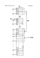
- storage in the storage memory 110 that is, log data storage processing when the log data has a size of 64 MB, for example, will be described in detail using the memory maps of FIGS.
- log data (64 MB) to be stored consists of “0001”, “0002”,..., “N”.
- the first work memory 101, the second work memory 102, and the storage memory 110 are in a state where no log data is stored. is there.
- a release flag (F00) that indicates release is written in the start address of the first storage area 101a of the first work memory 101 and the start address of the start storage area 102a of the second work memory 102, respectively.
- the first addresses (several bytes) of the first and second work memories 101 and 102 are reserved for flags, and log data is not written.
- log data “0001”, “0002”, “0003”, and “0004” transferred from the CPU 201 of the host computer 2 are stored in the four storage areas 101 a to 101 d of the first work memory 101 at the head.
- the data is stored sequentially from the storage area 101a in the order of addresses.
- the storage areas 101a to 101d of the first work memory 101 are filled with log data “0001”, “0002”, “0003”, and “0004”, then the log data “0005” is stored.
- ”,“ 0006 ”,“ 0007 ”, and“ 0008 ” are sequentially stored in the four storage areas 102 a to 102 d of the second work memory 102 in the order of addresses from the top storage area 102 a.
- the microcomputer 130 transfers the log data “0001”, “0002”, “0003”, “0004” stored in the first work memory 101 to the storage memory 110 and stores the data in the storage memory 110.
- the areas 110a to 110d are sequentially stored in the order of addresses from the top storage area 110a.
- the microcomputer 130 stores the log data in the first work memory 101.
- the completion flag FF00 is written in the storage area 101a storing the oldest log data “0001”.
- the log data “0008” is stored in the storage area 102 d at the end of the second work memory 102.
- the microcomputer 130 It is confirmed whether or not the completion flag FF00 is written in the first storage area 101a of the first work memory 101. If it is determined that the completion flag is written in the first storage area 101a of the first work memory 101, the log data “0009” is overwritten and stored in this storage area 101a. On the other hand, the microcomputer 130 transfers the log data “0005”, “0006”, “0007”, “0008” stored in the second work memory 102 to the storage memory 110 and stores the data in the storage memory 110.
- the areas 110e to 110h are sequentially stored in the order of addresses from the top storage area 110e.
- the log data transferred from the CPU 201 of the host computer 2 is stored in the first work memory 101 and the second work memory 102 by the ring buffer method. Overwrite the old ones in order.
- the microcomputer 130 (i) saves all the log data stored in the first work memory 101 as described above when all the storage areas 101a to 101d of the first work memory 101 are overwritten. The data is transferred to the memory 110 and stored sequentially in the order of addresses.
- the microcomputer 130 (ii) saves all the log data stored in the second work memory 102 as described above when all the storage areas 102a to 102d of the second work memory 102 are overwritten. The data is transferred to the memory 110 and stored sequentially in the order of addresses.
- the microcomputer 130 sequentially repeats (i) and (ii) above. Therefore, the log data can be efficiently transferred from the work memory 100 to the storage memory 110 and stored.
- the microcomputer 130 erases the oldest log data “0001”, “0002”, “0003”, “0004” among the log data stored in the storage memory 110, and stores the data in the storage memory 110.
- the storage areas 110a to 110d are emptied.
- the microcomputer 130 transfers the log data “N + 1”, “N + 2”, “N + 3”, “N + 4” stored in the first work memory 101 to the storage memory 110, and the storage memory 110 is vacant.
- the storage areas 110a to 110d are sequentially stored in the order of addresses from the top storage area 110a.
- the microcomputer 130 erases the oldest log data “0005”, “0006”, “0007”, “0008” from the log data stored in the storage area of the storage memory 110, and saves the memory 110 storage areas 110e to 110h are emptied.
- the log data is stored by sequentially erasing and rewriting the oldest log data stored in the storage memory 110 by the ring buffer method.
- the power interruption detection unit 190 detects the power interruption, and transmits a power interruption occurrence signal to the CPU 201 of the host computer 2, the competition control unit 121 of the FPGA 120, and the microcomputer 130.
- the CPU 201 and the microcomputer 130 receive the power-off occurrence signal, the CPU 201 and the microcomputer 130 stop accessing the work memory or the storage memory 110 before the power-off occurs.
- the contention control unit 121 serving as the shut-off control unit controls the first to fourth buffers 141, 142, 143, and 144, and works. Control to block access to the memory 100 or the storage memory 110 is performed.
- log data “0001”, “0002”, “0003”, and “0004” are saved from the first work memory 101 to the storage memory 110. If it is in the middle of the transfer to the microcomputer 130, the microcomputer 130 writes a transfer halfway flag informing the fact that the transfer is in progress to a predetermined location in the work memory 100. For example, the transfer-in-progress flag FFF0 is written to the top address of the top storage area 101a of the first work memory 101. After returning from the power interruption, the microcomputer 130 functions as a transfer state detection unit and detects the transfer halfway flag FFF0 written in the work memory 100, and the transfer log data stored in the storage memory 110 is stored.
- the microcomputer 130 again transfers the log data “0001”, “0002”, “0003”, and “0004” of the first work memory 101 to the storage memory 110 and stores them. For this reason, even if the transfer is in the middle of the transfer when the power is cut off, the other part of the log data remaining untransferred in the work memory 100 when the power is turned off is stored in the storage memory 110. Can be reliably transferred to. Therefore, a large amount of the log data can be stored more safely and reliably.
- the microcomputer 130 When the power interruption occurs, for example, as shown in FIG. 7, the microcomputer 130 is in the process of erasing the log data “0001”, “0002”, “0003”, “0004” in the storage memory 110. In this case, the microcomputer 130 writes an erasing flag indicating that the log data was being erased to a predetermined location in the work memory 100. For example, the erasing flag FFFF is written to the top address (address following the completion flag) of the top storage area 101a of the first work memory 101.
- the microcomputer 130 detects the erasure in progress flag FFFF written in the work memory 100 after returning from the power interruption, the erasure log data “0001”, “0002”, “0003” in the storage memory 110 is detected. , “0004” is deleted again. For this reason, even if the log data is being erased when the power is cut off, the log data remaining in the storage memory 110 without being erased can be reliably erased when the power is restored from the power cut.
- the backup device 1 can be realized with a relatively small size and low cost by using commercially available parts, and space and UPS costs can be omitted as compared with the case where a UPS is provided.
- the work memory 100 is composed of SRAM that can be backed up by the battery 150, but in the present invention, it may be composed of FeRAM.
- the backup device 1 is mounted on the board 1A, and the board 1A is detachably attached to the motherboard 2A of the host computer 2.
- the backup computer 1 It may be mounted on the motherboard 2A.
- the configuration of the backup device can be reduced as a whole together with the mother board.
- the release flag F00, the completion flag FF00, the transfer halfway flag FFF0, and the erasure halfway flag FFFF are written in the work memory 100.
- these flags may be written in the SRAM by providing an SRAM different from the work memory 100.
- the storage memory 110 is a NOR flash memory.
- NOR flash memory NOR flash memory
- a NAND flash memory or an SD card memory may be used.
- the FPGA 120 is used as the interface unit.
- an ASIC Application Specific Integrated Circuit
- the microcomputer 130 is used as the control unit.
- an FPGA may be used.
Landscapes
- Engineering & Computer Science (AREA)
- Theoretical Computer Science (AREA)
- Quality & Reliability (AREA)
- Physics & Mathematics (AREA)
- General Engineering & Computer Science (AREA)
- General Physics & Mathematics (AREA)
- Techniques For Improving Reliability Of Storages (AREA)
Abstract
L'invention concerne un dispositif de sauvegarde (1) comprenant une mémoire de travail (100) comportant une SRAM pour laquelle des données stockées dans celle-ci peuvent être sauvegardées par une batterie, et une mémoire à usage de stockage (110) comprenant une mémoire non volatile de densité d'enregistrement supérieure à la mémoire de travail (100). De plus l'invention concerne un micro-ordinateur (130) qui réalise une commande selon laquelle des données de journalisation qui ont été transférées à partir d'un ordinateur hôte (2) par l'intermédiaire d'une unité d'interface (120) et stockées dans la mémoire de travail (100) sont transférées vers la mémoire à usage de stockage (100) et stockées dans celle-ci.
Applications Claiming Priority (2)
| Application Number | Priority Date | Filing Date | Title |
|---|---|---|---|
| JP2011-132435 | 2011-06-14 | ||
| JP2011132435 | 2011-06-14 |
Publications (1)
| Publication Number | Publication Date |
|---|---|
| WO2012172708A1 true WO2012172708A1 (fr) | 2012-12-20 |
Family
ID=47356731
Family Applications (1)
| Application Number | Title | Priority Date | Filing Date |
|---|---|---|---|
| PCT/JP2011/078511 Ceased WO2012172708A1 (fr) | 2011-06-14 | 2011-12-09 | Dispositif de sauvegarde et procédé de fonctionnement du dispositif de sauvegarde |
Country Status (2)
| Country | Link |
|---|---|
| TW (1) | TW201250473A (fr) |
| WO (1) | WO2012172708A1 (fr) |
Cited By (1)
| Publication number | Priority date | Publication date | Assignee | Title |
|---|---|---|---|---|
| JP2016071494A (ja) * | 2014-09-29 | 2016-05-09 | 株式会社バッファロー | 通信装置、通信システム、通信装置における動作方法及びプログラム |
Families Citing this family (3)
| Publication number | Priority date | Publication date | Assignee | Title |
|---|---|---|---|---|
| TWI483105B (zh) * | 2013-01-31 | 2015-05-01 | Hon Hai Prec Ind Co Ltd | 主機板及其備份基板管理控制系統的方法 |
| TWI718317B (zh) * | 2016-11-04 | 2021-02-11 | 南韓商三星電子股份有限公司 | 資料儲存裝置及資料處理系統 |
| CN108021471A (zh) * | 2016-11-04 | 2018-05-11 | 三星电子株式会社 | 数据存储装置、数据处理系统及制造数据存储装置的方法 |
Citations (5)
| Publication number | Priority date | Publication date | Assignee | Title |
|---|---|---|---|---|
| US6571312B1 (en) * | 1999-02-19 | 2003-05-27 | Mitsubishi Denki Kabushiki Kaisha | Data storage method and data processing device using an erasure block buffer and write buffer for writing and erasing data in memory |
| US6795890B1 (en) * | 1999-02-19 | 2004-09-21 | Mitsubishi Denki Kabushiki Kaisha | Data storage method, and data processing device using an erasure block buffer and write buffer for writing and erasing data in memory |
| JP2008097635A (ja) * | 1999-02-19 | 2008-04-24 | Mitsubishi Electric Corp | 情報処理装置 |
| US20080104344A1 (en) * | 2006-10-25 | 2008-05-01 | Norio Shimozono | Storage system comprising volatile cache memory and nonvolatile memory |
| CA2714745A1 (fr) * | 2008-02-12 | 2009-08-20 | Netapp, Inc. | Architecture de systeme de stockage a supports hybrides |
-
2011
- 2011-12-09 WO PCT/JP2011/078511 patent/WO2012172708A1/fr not_active Ceased
-
2012
- 2012-01-12 TW TW101101176A patent/TW201250473A/zh unknown
Patent Citations (10)
| Publication number | Priority date | Publication date | Assignee | Title |
|---|---|---|---|---|
| US6571312B1 (en) * | 1999-02-19 | 2003-05-27 | Mitsubishi Denki Kabushiki Kaisha | Data storage method and data processing device using an erasure block buffer and write buffer for writing and erasing data in memory |
| US6795890B1 (en) * | 1999-02-19 | 2004-09-21 | Mitsubishi Denki Kabushiki Kaisha | Data storage method, and data processing device using an erasure block buffer and write buffer for writing and erasing data in memory |
| JP2008097635A (ja) * | 1999-02-19 | 2008-04-24 | Mitsubishi Electric Corp | 情報処理装置 |
| US20080104344A1 (en) * | 2006-10-25 | 2008-05-01 | Norio Shimozono | Storage system comprising volatile cache memory and nonvolatile memory |
| JP2008108026A (ja) * | 2006-10-25 | 2008-05-08 | Hitachi Ltd | 揮発性キャッシュメモリと不揮発性メモリとを備えたストレージシステム |
| CA2714745A1 (fr) * | 2008-02-12 | 2009-08-20 | Netapp, Inc. | Architecture de systeme de stockage a supports hybrides |
| WO2009102425A1 (fr) * | 2008-02-12 | 2009-08-20 | Netapp, Inc. | Architecture de système de stockage à supports hybrides |
| EP2263145A1 (fr) * | 2008-02-12 | 2010-12-22 | Netapp, Inc. | Architecture de système de stockage à supports hybrides |
| US20110035548A1 (en) * | 2008-02-12 | 2011-02-10 | Kimmel Jeffrey S | Hybrid media storage system architecture |
| JP2011515727A (ja) * | 2008-02-12 | 2011-05-19 | ネットアップ,インコーポレイテッド | ハイブリッド媒体ストレージシステムアーキテクチャ |
Cited By (1)
| Publication number | Priority date | Publication date | Assignee | Title |
|---|---|---|---|---|
| JP2016071494A (ja) * | 2014-09-29 | 2016-05-09 | 株式会社バッファロー | 通信装置、通信システム、通信装置における動作方法及びプログラム |
Also Published As
| Publication number | Publication date |
|---|---|
| TW201250473A (en) | 2012-12-16 |
Similar Documents
| Publication | Publication Date | Title |
|---|---|---|
| TWI540583B (zh) | 用於具有非揮發性記憶體之一系統的電力預算的動態分配 | |
| US8527693B2 (en) | Apparatus, system, and method for auto-commit memory | |
| US20190324859A1 (en) | Method and Apparatus for Restoring Data after Power Failure for An Open-Channel Solid State Drive | |
| US7739443B2 (en) | Memory controller, memory device and control method for the memory controller | |
| US20100235568A1 (en) | Storage device using non-volatile memory | |
| CN103678177B (zh) | 固态硬盘装置 | |
| US20160118130A1 (en) | Performance acceleration during shutdown of a data storage device | |
| US12086432B2 (en) | Gradually reclaim storage space occupied by a proof of space plot in a solid state drive | |
| US9582192B2 (en) | Geometry aware block reclamation | |
| CN104272390B (zh) | 包括闪存阵列和ram阵列的组成的存储器阵列且其具有数据写入ram阵列和从闪存阵列读取数据 | |
| TW201839613A (zh) | 數據儲存裝置及其操作方法 | |
| US20170060436A1 (en) | Technologies for managing a reserved high-performance memory region of a solid state drive | |
| CN113711189B (zh) | 用于管理固态驱动器上的降低电力故障能量需求的系统及方法 | |
| CN111414133B (zh) | 操作存储器控制器和存储器系统的方法以及存储器系统 | |
| KR20200032527A (ko) | 메모리 시스템의 동작 방법 및 메모리 시스템 | |
| US20240086076A1 (en) | Systems and methods for using a storage device as persistent memory | |
| US9965017B2 (en) | System and method for conserving energy in non-volatile dual inline memory modules | |
| JP2011018241A (ja) | 退避処理装置、退避処理方法およびストレージシステム | |
| CN109815158A (zh) | 进行系统备份的方法、记忆装置及控制器、及电子装置 | |
| WO2012172708A1 (fr) | Dispositif de sauvegarde et procédé de fonctionnement du dispositif de sauvegarde | |
| EP4320508A1 (fr) | Procédé et appareil pour réduire les collisions sur une puce nand dans un lecteur transistorisé | |
| US10795772B2 (en) | Memory system | |
| US20240264750A1 (en) | Atomic Operations Implemented using Memory Services of Data Storage Devices | |
| US20190073147A1 (en) | Control device, method and non-transitory computer-readable storage medium | |
| US20130080717A1 (en) | Information processing apparatus and control method |
Legal Events
| Date | Code | Title | Description |
|---|---|---|---|
| 121 | Ep: the epo has been informed by wipo that ep was designated in this application |
Ref document number: 11867634 Country of ref document: EP Kind code of ref document: A1 |
|
| NENP | Non-entry into the national phase |
Ref country code: DE |
|
| 122 | Ep: pct application non-entry in european phase |
Ref document number: 11867634 Country of ref document: EP Kind code of ref document: A1 |
|
| NENP | Non-entry into the national phase |
Ref country code: JP |