WO2012172904A1 - Dispositif de puissance et procédé de production d'un dispositif de puissance - Google Patents
Dispositif de puissance et procédé de production d'un dispositif de puissance Download PDFInfo
- Publication number
- WO2012172904A1 WO2012172904A1 PCT/JP2012/062316 JP2012062316W WO2012172904A1 WO 2012172904 A1 WO2012172904 A1 WO 2012172904A1 JP 2012062316 W JP2012062316 W JP 2012062316W WO 2012172904 A1 WO2012172904 A1 WO 2012172904A1
- Authority
- WO
- WIPO (PCT)
- Prior art keywords
- contact hole
- hole portion
- substrate
- insulating film
- side wall
- Prior art date
- Legal status (The legal status is an assumption and is not a legal conclusion. Google has not performed a legal analysis and makes no representation as to the accuracy of the status listed.)
- Ceased
Links
Images


Classifications
-
- H—ELECTRICITY
- H10—SEMICONDUCTOR DEVICES; ELECTRIC SOLID-STATE DEVICES NOT OTHERWISE PROVIDED FOR
- H10W—GENERIC PACKAGES, INTERCONNECTIONS, CONNECTORS OR OTHER CONSTRUCTIONAL DETAILS OF DEVICES COVERED BY CLASS H10
- H10W20/00—Interconnections in chips, wafers or substrates
- H10W20/01—Manufacture or treatment
- H10W20/071—Manufacture or treatment of dielectric parts thereof
- H10W20/081—Manufacture or treatment of dielectric parts thereof by forming openings in the dielectric parts
- H10W20/082—Manufacture or treatment of dielectric parts thereof by forming openings in the dielectric parts the openings being tapered via holes
-
- H—ELECTRICITY
- H10—SEMICONDUCTOR DEVICES; ELECTRIC SOLID-STATE DEVICES NOT OTHERWISE PROVIDED FOR
- H10D—INORGANIC ELECTRIC SEMICONDUCTOR DEVICES
- H10D84/00—Integrated devices formed in or on semiconductor substrates that comprise only semiconducting layers, e.g. on Si wafers or on GaAs-on-Si wafers
- H10D84/01—Manufacture or treatment
- H10D84/02—Manufacture or treatment characterised by using material-based technologies
- H10D84/05—Manufacture or treatment characterised by using material-based technologies using Group III-V technology
-
- H—ELECTRICITY
- H10—SEMICONDUCTOR DEVICES; ELECTRIC SOLID-STATE DEVICES NOT OTHERWISE PROVIDED FOR
- H10W—GENERIC PACKAGES, INTERCONNECTIONS, CONNECTORS OR OTHER CONSTRUCTIONAL DETAILS OF DEVICES COVERED BY CLASS H10
- H10W20/00—Interconnections in chips, wafers or substrates
- H10W20/01—Manufacture or treatment
- H10W20/031—Manufacture or treatment of conductive parts of the interconnections
- H10W20/032—Manufacture or treatment of conductive parts of the interconnections of conductive barrier, adhesion or liner layers
- H10W20/033—Manufacture or treatment of conductive parts of the interconnections of conductive barrier, adhesion or liner layers in openings in dielectrics
- H10W20/036—Manufacture or treatment of conductive parts of the interconnections of conductive barrier, adhesion or liner layers in openings in dielectrics the barrier, adhesion or liner layers being within a main fill metal
Definitions
- the present invention relates to a power device and a method for manufacturing the power device, and more particularly to a wiring structure of a GaN-based FET.
- Compound semiconductors such as gallium nitride have higher electron mobility than silicon semiconductors, and have little change in characteristics even at high temperature operation, and have high breakdown voltage characteristics. It is attracting attention as a material for devices. In particular, utilization as a small semiconductor device capable of high withstand voltage and large current operation is desired.
- the internal wiring layer connecting the source electrode, the drain electrode, and the gate electrode ensures high reliability. And what is formed at low cost is desired.
- the current in the contact hole portion is concentrated, and in GaN using high mobility, the distance between the source and the drain is also short, and thus many contact holes must be provided. It will be costly.
- the contact hole portion 110a formed in the interlayer insulating film 110 is substantially perpendicular to the substrate plane as shown in FIG. It has a side wall W.
- metal Al or AlCu
- the film thickness of the wiring layer 112 in the side wall W portion is reduced. For this reason, the thin part of the wiring layer becomes a weak point where electromigration is likely to occur, and there is a problem that the electromigration resistance is lowered and the long-term reliability is inferior.
- an object of the present invention is to provide a power device and a power device manufacturing method capable of improving electromigration resistance and long-term reliability without using an organic material which causes film peeling.
- the power device of the present invention is: A substrate, A GaN-based semiconductor layer formed on the substrate; An electrode formed on the GaN-based semiconductor layer, or formed to be at least partially embedded in the upper portion of the GaN-based semiconductor layer; An interlayer insulating film made of silicon oxide or silicon oxynitride formed on the GaN-based semiconductor layer; A first contact hole portion formed on at least a part of the electrode and in the interlayer insulating film and having a first sidewall substantially perpendicular to the substrate plane; A second contact formed on the interlayer insulating film so as to gradually spread upward from the upper edge of the first side wall of the first contact hole portion and having a second side wall inclined with respect to the substrate plane.
- the hall A wiring layer formed in the first contact hole portion and in the second contact hole portion and on the interlayer insulating film; The wiring layer has a thickness greater than a dimension of the first side wall in the substrate thickness direction in the first contact hole portion.
- the GaN-based semiconductor layer is a semiconductor layer made of a mixed crystal material based on GaN (gallium nitride), and includes a compound such as GaN, AlGaN, InGaN, or AlInGaN.
- the wiring layer having a thickness larger than the dimension of the first sidewall in the substrate thickness direction is formed at least in the first contact hole portion in the first and second contact hole portions and on the interlayer insulating film.
- a thick interlayer insulating film can be formed and a wiring layer with a uniform thickness can be formed.
- electromigration that tends to occur in the thin wiring layer portion can be effectively suppressed. Therefore, it is possible to improve electromigration resistance and long-term reliability without using an organic material that causes film peeling for the interlayer insulating film.
- an FET using a GaN-based semiconductor capable of operating at a high voltage, a large current, and a high temperature as a power device has a high current density in a wiring layer connected to a source electrode and a drain electrode and operates at a high temperature. Although migration tends to occur, the effect of the present invention is extremely effective.
- the wiring layer is a wiring layer having a multilayer structure in which a first barrier layer, a first wiring layer, a second barrier layer, a second wiring layer, and a third barrier layer are sequentially stacked from the first barrier layer,
- the first wiring layer is thicker than the dimension of the first sidewall in the substrate thickness direction at least in the first contact hole portion.
- the first barrier layer, the first wiring layer, the second barrier layer, the second wiring layer, and the third barrier layer are laminated in order from the first barrier layer.
- the wiring layer is drawn out from the first contact hole portion through the second contact hole portion onto the interlayer insulating film without a steep step.
- the first to third barrier layers allow diffusion of the wiring layer material in the upward or downward direction in the first wiring layer and the second wiring layer without disturbing the multilayer structure of the barrier layer and causing the barrier layer to be interrupted or thinned. It can be reliably suppressed, and electromigration resistance and long-term reliability can be further improved.
- the dimension of the first side wall of the first contact hole portion in the substrate thickness direction is smaller than the dimension of the second side wall of the second contact hole portion in the substrate thickness direction.
- the dimension of the first sidewall of the first contact hole portion in the substrate thickness direction smaller than the dimension of the second sidewall of the second contact hole portion in the substrate thickness direction, It can be ensured that a thin portion is not formed in the wiring layer on the first side wall of the first contact hole portion substantially perpendicular to the substrate plane.
- the electrodes are formed on the GaN-based semiconductor layer so as to be spaced from each other, or are formed so as to be at least partially embedded in the upper portion of the GaN-based semiconductor layer.
- the wiring layer connected to the source electrode through the first and second contact hole portions extends above the gate electrode and on the interlayer insulating film from the source electrode side toward the gate electrode side. The portion formed to serve as the field plate portion.
- the gate electrode in the wiring layer connected to the source electrode through the first and second contact hole portions, extends from the source electrode side to the drain electrode side above the gate electrode and on the interlayer insulating film.
- the portion formed in this manner also serves as the field plate portion, thereby improving the breakdown voltage by relaxing the electric field strength in the GaN-based semiconductor layer while improving the resistance to electromigration and long-term reliability.
- the dimension of the inclined surface of the second side wall of the second contact hole portion at a cut surface by a plane that passes through substantially the center of the second contact hole portion and is perpendicular to the substrate plane is long.
- the inclination angle of the second side wall with respect to the substrate plane is preferably 45 degrees or less, more preferably 30 degrees or less, whereby the wiring layer can have a more uniform thickness.
- Forming a GaN-based semiconductor layer on a substrate Forming an electrode on the GaN-based semiconductor layer, or forming an electrode so as to be at least partially embedded in the upper portion of the GaN-based semiconductor layer; Forming an interlayer insulating film made of silicon oxide or silicon oxynitride on the GaN-based semiconductor layer on which the electrode is formed; Forming a second contact hole portion having a second sidewall inclined with respect to the substrate plane by wet etching so as to gradually spread upward in the interlayer insulating film; A first contact hole portion having a first side wall substantially perpendicular to the substrate plane so that at least a partial region of the electrode is exposed at a bottom portion of the second contact hole portion of the interlayer insulating film; Forming by dry etching; A wiring layer having a thickness greater than the dimension of the first sidewall in the substrate thickness direction at least in the first contact hole portion in the first contact hole portion, the second contact hole portion, and the interlayer
- the wiring layer having a thickness larger than the dimension of the first sidewall in the substrate thickness direction is formed at least in the first contact hole portion in the first and second contact hole portions and on the interlayer insulating film.
- a thin portion is not formed in the wiring layer on the first sidewall of the first contact hole portion and the second sidewall of the second contact hole portion. Migration can be effectively suppressed. Therefore, it is possible to improve electromigration resistance and long-term reliability without using an organic material that causes film peeling for the interlayer insulating film.
- the sizes of the first and second contact hole portions can be made uniform, variation in characteristics between elements in the same wafer can be suppressed.
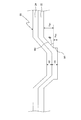
- FIG. 1 is a cross-sectional view of a power device before forming a wiring layer according to a first embodiment of the present invention.
- FIG. 2 is a cross-sectional view for explaining the manufacturing process of the power device.
- FIG. 3 is a cross-sectional view for explaining a manufacturing process subsequent to FIG.
- FIG. 4 is a cross-sectional view for explaining a manufacturing process subsequent to FIG.
- FIG. 5 is a cross-sectional view for explaining the manufacturing process subsequent to FIG.
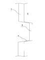
- FIG. 6 is a cross-sectional view of a power device according to the second embodiment of the present invention.
- FIG. 7 is a plan view of the main part of the power device.
- FIG. 8 is a cross-sectional view of the wiring layer of the power device.
- FIG. 9 is a schematic diagram of an enlarged cross section of the main part of the power device.
- FIG. 10 is a cross-sectional view of a main part of a conventional power device.
- FIG. 1 is a sectional view of a power device according to the first embodiment of the present invention.
- the power device of the first embodiment is a GaN-based HFET (Hetero-junction Field Effect Transistor).
- the power device includes a superlattice buffer layer 2 (AlGaN / GaN), a channel layer 3 (GaN), and an example of a GaN-based semiconductor layer on an Si substrate 1.
- the barrier layer 4 (AlGaN) is formed in this order.
- a source electrode 5 and a drain electrode 6 are formed on the barrier layer 4 at an interval.
- a gate electrode 7 is formed on the barrier layer 4 in a region between the source electrode 5 and the drain electrode 6.
- the source electrode 5 and the drain electrode 6 are an alloy made of Hf / Al, and the gate electrode 7 is made of WN.
- a sapphire substrate may be used instead of the Si substrate 1, or a GaN substrate may be used.
- a superlattice buffer layer 2 two layers having different Al compositions in an AlGaN multilayer structure may be stacked, or a low temperature buffer layer may be used.
- 2DEG two-dimensional electron gas
- the gate electrode 7 is formed by selecting a material for forming a Schottky barrier with respect to the barrier layer 4. Ni / Au or TiN can also be used as the gate electrode material.
- an insulating film made of silicon nitride (SiN) is formed as the surface protective film 8 on the barrier layer 4 on which the gate electrode 7 is formed.
- the surface protective film 8 also functions as a film for suppressing collapse.
- the surface protective film does not have to be a single layer, and may be a multilayer film. In the case of a multilayer film, a silicon oxide (SiO 2 ) film may be used as an upper layer.
- the source electrode 5 and the drain electrode 6 are formed in the opening.
- the source electrode 6 and the drain electrode 7 only need to form an ohmic junction with 2DEG (two-dimensional electron gas), for example, a recess structure from which the barrier layer is removed, or an n-type barrier by doping the barrier layer.
- An ohmic electrode may be formed in the layer.
- the wiring layer is electrically connected to the source electrode 5.
- the drain electrode 7 (not shown) is also electrically connected to another wiring layer.
- silicon oxide SiO 2
- a film having a thickness of 1000 nm is formed on the barrier layer 4 (AlGaN) on which the source electrode 5, the drain electrode 6, the gate electrode 7, and the surface protective film 8 shown in FIG. 2 are formed.
- a photoresist 11 is deposited, the photoresist 11 is exposed and developed, and an opening 11a is formed in a region of the photoresist 11 where the source electrode 5 (ohmic electrode) is to be formed. To do.
- an opening having a depth of 600 nm is formed as a second contact hole portion 10b in the interlayer insulating film 10 by wet etching (isotropic etching) using buffer hydrofluoric acid.
- An opening to be the second contact hole portion 10 b of the interlayer insulating film 10 is formed so as to partially enter the lower portion of the photoresist 11.
- an opening having a depth of 400 nm is formed as a first contact hole 10a in the interlayer insulating film 10 by dry etching (anisotropic etching) using the photoresist 11 as a mask.
- the source electrode 5 (ohmic electrode) is exposed.
- the first contact hole portion having the first side wall W1 substantially perpendicular to the substrate plane by utilizing the characteristics of isotropic etching and anisotropic etching. 10a and a second contact hole portion 10b having a second side wall W2 inclined with respect to the substrate plane.
- the first side wall W1 of the first contact hole portion 10a is formed with an inclination of 90 to 80 degrees with respect to the substrate plane
- the second side wall W2 of the second contact hole portion 10b is on the substrate plane.
- 1500 nm of TiN / Al / TiN is deposited on the Si substrate 1 (shown in FIG. 1) by sputtering.
- the wiring layer 12 is formed by etching leaving the wiring region (including the contact region).
- a wiring structure having a uniform thickness including the interlayer insulating film 10 made of thick silicon oxide (SiO 2 ) can be formed.
- silicon oxide SiO 2
- silicon oxynitride containing N may be used, and B or P may be contained if the amount is small.
- AlCu may be used as the wiring layer.
- Si in the first side wall W1 is formed in the first and second contact hole portions 10a and 10b and on the interlayer insulating film 10 at least in the first contact hole portion 10a.
- the wiring layer 12 having a film thickness larger than the dimension in the thickness direction of the substrate 1
- the interlayer insulating film 10 having a large film thickness can be formed, and the wiring layer 12 having a uniform thickness can be formed.
- a thin portion is not formed in the wiring layer 12, so that an electro which is likely to occur in the thin wiring layer portion is formed. Migration can be effectively suppressed. Therefore, it is possible to improve electromigration resistance and long-term reliability without using an organic material that causes film peeling for the interlayer insulating film.
- the method for manufacturing a power device it is possible to make the sizes of the first and second contact hole portions 10a and 10b uniform, and to suppress the characteristic variation between elements in the same wafer.
- the design value of the current density of the wiring layer 12 is 1.39 ⁇ 10 5 [A / cm 2 ], which is a design condition suitable for large current operation.
- the current density of the wiring layer connected to the source electrode and the drain electrode is high, and thus, even under conditions where electromigration tends to occur, a high effect of improving electromigration resistance and long-term reliability can be obtained.
- the dimension in the substrate thickness direction of the first side wall W1 of the first contact hole portion 10a smaller than the dimension in the substrate thickness direction of the second side wall W2 of the second contact hole portion 10b, It is possible to reliably prevent the thin portion of the wiring layer 12 from being formed on the first side wall W1 of the first contact hole portion 10a substantially perpendicular to the substrate plane.
- the wiring layer 12 can be smoothly drawn out on the interlayer insulating film 10 through 10b without a step, and it is possible to surely prevent the thin portion where the electromigration easily occurs from being formed in the wiring layer 12.
- the interlayer insulating film is formed above the gate electrode 7 and from the source electrode 5 side to the drain electrode 6 side. 10 so that the portion formed so as to extend also serves as a field plate portion can improve the electromigration resistance and the long-term reliability, and reduce the electric field strength in the channel layer 3 and the barrier layer 4. Thus, the breakdown voltage can be improved.
- FIG. 6 shows a cross-sectional view of a power device according to the second embodiment of the present invention.
- the power device according to the second embodiment has the same configuration as that of the power device according to the first embodiment except for the wiring layer.
- the power device of the second embodiment is the same as the power device of the first embodiment until the step of forming the first and second contact hole portions 10a and 10b in FIG.
- the wiring layer 20 having a two-layer structure is formed by etching using a photo process while leaving the wiring region (including the contact region).
- FIG. 7 shows a plan view of the main part of the power device, which is a rectangular shape formed on at least a part of the source electrode 5 (shown in FIG. 1) or the drain electrode 6 (shown in FIG. 1).
- First and second contact hole portions 10a and 10b having a trench structure are formed, and a wiring layer 20 is formed in the first and second contact hole portions 10a and 10b and on the interlayer insulating film 10 (shown in FIG. 1). ing.
- the wiring layer 20 includes a barrier metal layer 21 (TiN with a thickness of 100 nm) as an example of a first barrier layer, a first wiring layer 22 (AlCu with a thickness of 600 nm), a second Barrier metal layer 23 (100 nm thick TiN) as an example of the barrier layer, first wiring layer 24 (600 nm thick AlCu), and barrier metal layer 25 (100 nm thick as the third barrier layer) TiN) is stacked in order from the bottom.
- a barrier metal layer 21 TiN with a thickness of 100 nm
- first wiring layer 22 AlCu with a thickness of 600 nm
- a second Barrier metal layer 23 100 nm thick TiN
- first wiring layer 24 600 nm thick AlCu
- barrier metal layer 25 100 nm thick as the third barrier layer TiN
- the power device of the second embodiment has the same effect as the power device of the first embodiment.
- the barrier metal layer 21, the first wiring layer 22, the barrier metal layer 23, the second wiring layer 24, and the barrier metal layer 25 are laminated in order from the barrier metal layer 21.
- wiring is performed from the first contact hole portion 10a to the interlayer insulating film 10 via the second contact hole portion 10b without a steep step. Since the layer 20 is pulled out, the multilayer structure of the wiring layer 20 is not disturbed, and the barrier metal layers 21, 23, 25 are not interrupted or thinned.
- the diffusion of the wiring layer material (mainly Al in the second embodiment) in the upward direction or the downward direction is ensured by the barrier metal layers 21, 23, 25. It can be suppressed and the resistance to electromigration and long-term reliability can be further improved.
- FIG. 9 is a schematic diagram of an enlarged cross section of the main part of the power device.
- H1 is the thickness of the first wiring layer 22 in the wiring layer 20 having a two-layer structure
- H2 is a two-layer structure.
- the thickness of the second wiring layer 24 H W1 is the dimension of the first side wall W1 of the first contact hole portion 10a in the substrate thickness direction
- H W2 is the second thickness of the second contact hole portion 10b.
- the dimension of the second side wall W2 in the substrate thickness direction, ⁇ is the inclination angle of the second side wall W2 of the second contact hole portion 10b with respect to the substrate plane.
- the barrier metal layers 21, 23, and 25 are omitted.
- the thickness H1 of the first wiring layer 22 the relationship between the first substrate thickness dimension H W1 of the side wall W1 of the first contact hole section 10a, H1> H W1 The conditions are satisfied.
- the service life can be drastically improved.
- Table 1 shows the result of calculating the lifetimes of the one-layer wiring layer of the first embodiment and the two-layer wiring layer of the second embodiment by performing an acceleration test.
- the environmental temperature is set to 250 ° C., and a constant current of 1.33 ⁇ 10 6 [A / cm 2 ] is passed from the constant current source to the wiring layer to be tested, and the change with time of the voltage across the wiring layer is measured. Measure the change of the resistance of the wiring layer over time based on the constant current flowing in the wiring layer and the voltage across the wiring layer, and determine that each of the wiring layers is defective when the resistance of the wiring layer fluctuates 10% from the initial value. The life of the wiring layer was determined.
- A is the shape factor
- J is the current density
- Ea is the activation energy (specific to the Al wiring)
- k is the Boltzmann constant
- T is the absolute temperature.
- the absolute temperature T is an absolute temperature estimated when a temperature characteristic is measured in advance and a current is passed at 1.33 ⁇ 10 6 [A / cm 2 ].
- J is 1.4 ⁇ 10 5 [A / cm 2 ].
- uniform wiring can be obtained by setting the first wiring layer 22 (AlCu) of the first layer to a thickness of 600 nm and thicker than the height of the first side wall W1. As a result, the electromigration characteristics could be sufficiently improved.
- the contact hole has two steps, and the thickness of the first wiring layer 22 is the depth of the first contact hole portion in the first step.
- the GaN HFET in which the source electrode 5, the drain electrode 6, and the gate electrode 7 are formed on the barrier layer 4 as the power device has been described.
- at least one GaN HFET is formed on the GaN semiconductor layer.
- the present invention may be applied to a power device having a source electrode and a drain electrode formed so as to be spaced from each other so that the portion is embedded.
- the power device when the source electrode and the drain electrode are all formed on the GaN-based semiconductor layer with a space between them, and when the GaN-based semiconductor layer is etched, the power device is spaced 2 from each other.
- the source electrode and the drain electrode are formed so that a part of the lower side of the source electrode and the drain electrode is embedded in each recess.
- one of the source electrode and the drain electrode may be entirely formed on the GaN-based semiconductor layer, and the other of the source electrode or the drain electrode may be at least partially formed in the GaN-based semiconductor layer.
- the GaN-based semiconductor layer of the power device according to the present invention only needs to be expressed by Al x In y Ga 1-xy N (x ⁇ 0, y ⁇ 0, 0 ⁇ x + y ⁇ 1). That is, the GaN-based semiconductor layer is not limited to GaN, but may be AlGaN, InGaN, or AlInGaN.
- the power device of the present invention is not limited to the HFET of the first and second embodiments, but may be a field effect transistor having another configuration.
Landscapes
- Electrodes Of Semiconductors (AREA)
- Internal Circuitry In Semiconductor Integrated Circuit Devices (AREA)
- Junction Field-Effect Transistors (AREA)
Abstract
L'invention concerne un dispositif comprenant : un film (10) d'isolation inter-couches comportant de l'oxyde de silicium (SiO2) formé par-dessus une couche barrière (4) (AlGaN) ; une première partie (11a) de trou de contact formée par-dessus une électrode (5) de source du film (10) d'isolation inter-couches et présentant une première paroi latérale (W1) approximativement perpendiculaire au plan du substrat ; une deuxième partie (11b) de trou de contact formée dans le film (10) d'isolation inter-couches de manière à s'élargir progressivement en direction de la face supérieure à partir du bord supérieur de la première paroi latérale (W1) de la première partie (11a) de trou de contact, et présentant une deuxième paroi latérale (W2) inclinée par rapport au plan du substrat ; et une couche (12) de câblage formée à l'intérieur des première et deuxième parties (11a, 11b) de trou de contact et par-dessus le film (10) d'isolation inter-couches. L'épaisseur de la couche (12) de câblage est supérieure à la dimension de la première paroi latérale (W1) de la première partie (11a) de trou de contact dans la direction de l'épaisseur du substrat. Un dispositif de puissance caractérisé par une résistance à l'électromigration et une fiabilité à long terme améliorées est ainsi réalisé, sans utiliser de matériaux organiques susceptibles de causer un décollement du film.
Applications Claiming Priority (2)
| Application Number | Priority Date | Filing Date | Title |
|---|---|---|---|
| JP2011133597A JP5171996B2 (ja) | 2011-06-15 | 2011-06-15 | パワーデバイス |
| JP2011-133597 | 2011-06-15 |
Publications (1)
| Publication Number | Publication Date |
|---|---|
| WO2012172904A1 true WO2012172904A1 (fr) | 2012-12-20 |
Family
ID=47356899
Family Applications (1)
| Application Number | Title | Priority Date | Filing Date |
|---|---|---|---|
| PCT/JP2012/062316 Ceased WO2012172904A1 (fr) | 2011-06-15 | 2012-05-14 | Dispositif de puissance et procédé de production d'un dispositif de puissance |
Country Status (2)
| Country | Link |
|---|---|
| JP (1) | JP5171996B2 (fr) |
| WO (1) | WO2012172904A1 (fr) |
Citations (4)
| Publication number | Priority date | Publication date | Assignee | Title |
|---|---|---|---|---|
| JPH06216062A (ja) * | 1992-11-26 | 1994-08-05 | Sony Corp | 半導体装置の製造方法 |
| JPH07201991A (ja) * | 1993-12-28 | 1995-08-04 | Sony Corp | 半導体装置およびその製造方法 |
| JP2003152075A (ja) * | 2001-11-09 | 2003-05-23 | Sony Corp | 半導体装置の製造方法 |
| JP2006286952A (ja) * | 2005-03-31 | 2006-10-19 | Eudyna Devices Inc | 半導体装置およびその製造方法 |
-
2011
- 2011-06-15 JP JP2011133597A patent/JP5171996B2/ja not_active Expired - Fee Related
-
2012
- 2012-05-14 WO PCT/JP2012/062316 patent/WO2012172904A1/fr not_active Ceased
Patent Citations (4)
| Publication number | Priority date | Publication date | Assignee | Title |
|---|---|---|---|---|
| JPH06216062A (ja) * | 1992-11-26 | 1994-08-05 | Sony Corp | 半導体装置の製造方法 |
| JPH07201991A (ja) * | 1993-12-28 | 1995-08-04 | Sony Corp | 半導体装置およびその製造方法 |
| JP2003152075A (ja) * | 2001-11-09 | 2003-05-23 | Sony Corp | 半導体装置の製造方法 |
| JP2006286952A (ja) * | 2005-03-31 | 2006-10-19 | Eudyna Devices Inc | 半導体装置およびその製造方法 |
Also Published As
| Publication number | Publication date |
|---|---|
| JP5171996B2 (ja) | 2013-03-27 |
| JP2013004691A (ja) | 2013-01-07 |
Similar Documents
| Publication | Publication Date | Title |
|---|---|---|
| JP5396369B2 (ja) | 半導体基板構造および半導体素子 | |
| CN110071173B (zh) | 半导体装置及其制造方法 | |
| TWI663698B (zh) | 半導體裝置 | |
| CN111509041B (zh) | 半导体器件及其制造方法 | |
| JP6280796B2 (ja) | ショットキーダイオードおよび高電子移動度トランジスタを備えた半導体デバイスの製造方法 | |
| US9768257B2 (en) | Semiconductor device | |
| US8963203B2 (en) | Nitride semiconductor device and method for manufacturing same | |
| CN104425482A (zh) | 半导体装置 | |
| CN113016074A (zh) | 半导体器件及其制造方法 | |
| TW201633532A (zh) | 半導體裝置及半導體裝置之製造方法 | |
| CN103503152A (zh) | 用于半导体器件的电极配置 | |
| CN112531025B (zh) | 高电子迁移率晶体管 | |
| CN102623498A (zh) | 半导体元件 | |
| US20130140630A1 (en) | Trench schottky diode and manufacturing method thereof | |
| CN114586175B (zh) | 半导体器件以及制造半导体器件的方法 | |
| TWI624872B (zh) | 氮化物半導體元件 | |
| CN107863294A (zh) | 半导体晶片和方法 | |
| JP2009212472A (ja) | 窒化物半導体素子 | |
| TW201947766A (zh) | 高電子遷移率電晶體 | |
| CN105895683A (zh) | 半导体器件及制造方法 | |
| JP2009152462A (ja) | 窒化物半導体素子および窒化物半導体素子の製造方法 | |
| CN112750700A (zh) | 高电子迁移率晶体管及其制作方法 | |
| US20130341640A1 (en) | Semiconductor device and method for manufacturing same | |
| TWI692039B (zh) | 半導體裝置的製作方法 | |
| CN114975614A (zh) | 高电子迁移率晶体管及其制作方法 |
Legal Events
| Date | Code | Title | Description |
|---|---|---|---|
| 121 | Ep: the epo has been informed by wipo that ep was designated in this application |
Ref document number: 12799741 Country of ref document: EP Kind code of ref document: A1 |
|
| NENP | Non-entry into the national phase |
Ref country code: DE |
|
| 122 | Ep: pct application non-entry in european phase |
Ref document number: 12799741 Country of ref document: EP Kind code of ref document: A1 |