WO2012176467A1 - Feuille de verre avec membrane conductrice transparente et procédé de fabrication de celle-ci - Google Patents
Feuille de verre avec membrane conductrice transparente et procédé de fabrication de celle-ci Download PDFInfo
- Publication number
- WO2012176467A1 WO2012176467A1 PCT/JP2012/004055 JP2012004055W WO2012176467A1 WO 2012176467 A1 WO2012176467 A1 WO 2012176467A1 JP 2012004055 W JP2012004055 W JP 2012004055W WO 2012176467 A1 WO2012176467 A1 WO 2012176467A1
- Authority
- WO
- WIPO (PCT)
- Prior art keywords
- layer
- transparent conductive
- conductive film
- glass plate
- film
- Prior art date
- Legal status (The legal status is an assumption and is not a legal conclusion. Google has not performed a legal analysis and makes no representation as to the accuracy of the status listed.)
- Ceased
Links
Images





Classifications
-
- C—CHEMISTRY; METALLURGY
- C03—GLASS; MINERAL OR SLAG WOOL
- C03C—CHEMICAL COMPOSITION OF GLASSES, GLAZES OR VITREOUS ENAMELS; SURFACE TREATMENT OF GLASS; SURFACE TREATMENT OF FIBRES OR FILAMENTS MADE FROM GLASS, MINERALS OR SLAGS; JOINING GLASS TO GLASS OR OTHER MATERIALS
- C03C17/00—Surface treatment of glass, not in the form of fibres or filaments, by coating
- C03C17/34—Surface treatment of glass, not in the form of fibres or filaments, by coating with at least two coatings having different compositions
- C03C17/3411—Surface treatment of glass, not in the form of fibres or filaments, by coating with at least two coatings having different compositions with at least two coatings of inorganic materials
-
- C—CHEMISTRY; METALLURGY
- C23—COATING METALLIC MATERIAL; COATING MATERIAL WITH METALLIC MATERIAL; CHEMICAL SURFACE TREATMENT; DIFFUSION TREATMENT OF METALLIC MATERIAL; COATING BY VACUUM EVAPORATION, BY SPUTTERING, BY ION IMPLANTATION OR BY CHEMICAL VAPOUR DEPOSITION, IN GENERAL; INHIBITING CORROSION OF METALLIC MATERIAL OR INCRUSTATION IN GENERAL
- C23C—COATING METALLIC MATERIAL; COATING MATERIAL WITH METALLIC MATERIAL; SURFACE TREATMENT OF METALLIC MATERIAL BY DIFFUSION INTO THE SURFACE, BY CHEMICAL CONVERSION OR SUBSTITUTION; COATING BY VACUUM EVAPORATION, BY SPUTTERING, BY ION IMPLANTATION OR BY CHEMICAL VAPOUR DEPOSITION, IN GENERAL
- C23C16/00—Chemical coating by decomposition of gaseous compounds, without leaving reaction products of surface material in the coating, i.e. chemical vapour deposition [CVD] processes
- C23C16/22—Chemical coating by decomposition of gaseous compounds, without leaving reaction products of surface material in the coating, i.e. chemical vapour deposition [CVD] processes characterised by the deposition of inorganic material, other than metallic material
- C23C16/30—Deposition of compounds, mixtures or solid solutions, e.g. borides, carbides, nitrides
- C23C16/40—Oxides
- C23C16/407—Oxides of zinc, germanium, cadmium, indium, tin, thallium or bismuth
-
- C—CHEMISTRY; METALLURGY
- C23—COATING METALLIC MATERIAL; COATING MATERIAL WITH METALLIC MATERIAL; CHEMICAL SURFACE TREATMENT; DIFFUSION TREATMENT OF METALLIC MATERIAL; COATING BY VACUUM EVAPORATION, BY SPUTTERING, BY ION IMPLANTATION OR BY CHEMICAL VAPOUR DEPOSITION, IN GENERAL; INHIBITING CORROSION OF METALLIC MATERIAL OR INCRUSTATION IN GENERAL
- C23C—COATING METALLIC MATERIAL; COATING MATERIAL WITH METALLIC MATERIAL; SURFACE TREATMENT OF METALLIC MATERIAL BY DIFFUSION INTO THE SURFACE, BY CHEMICAL CONVERSION OR SUBSTITUTION; COATING BY VACUUM EVAPORATION, BY SPUTTERING, BY ION IMPLANTATION OR BY CHEMICAL VAPOUR DEPOSITION, IN GENERAL
- C23C16/00—Chemical coating by decomposition of gaseous compounds, without leaving reaction products of surface material in the coating, i.e. chemical vapour deposition [CVD] processes
- C23C16/56—After-treatment
-
- H—ELECTRICITY
- H10—SEMICONDUCTOR DEVICES; ELECTRIC SOLID-STATE DEVICES NOT OTHERWISE PROVIDED FOR
- H10F—INORGANIC SEMICONDUCTOR DEVICES SENSITIVE TO INFRARED RADIATION, LIGHT, ELECTROMAGNETIC RADIATION OF SHORTER WAVELENGTH OR CORPUSCULAR RADIATION
- H10F77/00—Constructional details of devices covered by this subclass
- H10F77/30—Coatings
- H10F77/306—Coatings for devices having potential barriers
- H10F77/311—Coatings for devices having potential barriers for photovoltaic cells
- H10F77/315—Coatings for devices having potential barriers for photovoltaic cells the coatings being antireflective or having enhancing optical properties
-
- H—ELECTRICITY
- H10—SEMICONDUCTOR DEVICES; ELECTRIC SOLID-STATE DEVICES NOT OTHERWISE PROVIDED FOR
- H10F—INORGANIC SEMICONDUCTOR DEVICES SENSITIVE TO INFRARED RADIATION, LIGHT, ELECTROMAGNETIC RADIATION OF SHORTER WAVELENGTH OR CORPUSCULAR RADIATION
- H10F77/00—Constructional details of devices covered by this subclass
- H10F77/70—Surface textures, e.g. pyramid structures
- H10F77/707—Surface textures, e.g. pyramid structures of the substrates or of layers on substrates, e.g. textured ITO layer on a glass substrate
-
- C—CHEMISTRY; METALLURGY
- C03—GLASS; MINERAL OR SLAG WOOL
- C03C—CHEMICAL COMPOSITION OF GLASSES, GLAZES OR VITREOUS ENAMELS; SURFACE TREATMENT OF GLASS; SURFACE TREATMENT OF FIBRES OR FILAMENTS MADE FROM GLASS, MINERALS OR SLAGS; JOINING GLASS TO GLASS OR OTHER MATERIALS
- C03C2217/00—Coatings on glass
- C03C2217/40—Coatings comprising at least one inhomogeneous layer
-
- C—CHEMISTRY; METALLURGY
- C03—GLASS; MINERAL OR SLAG WOOL
- C03C—CHEMICAL COMPOSITION OF GLASSES, GLAZES OR VITREOUS ENAMELS; SURFACE TREATMENT OF GLASS; SURFACE TREATMENT OF FIBRES OR FILAMENTS MADE FROM GLASS, MINERALS OR SLAGS; JOINING GLASS TO GLASS OR OTHER MATERIALS
- C03C2217/00—Coatings on glass
- C03C2217/90—Other aspects of coatings
- C03C2217/94—Transparent conductive oxide layers [TCO] being part of a multilayer coating
-
- H—ELECTRICITY
- H10—SEMICONDUCTOR DEVICES; ELECTRIC SOLID-STATE DEVICES NOT OTHERWISE PROVIDED FOR
- H10F—INORGANIC SEMICONDUCTOR DEVICES SENSITIVE TO INFRARED RADIATION, LIGHT, ELECTROMAGNETIC RADIATION OF SHORTER WAVELENGTH OR CORPUSCULAR RADIATION
- H10F77/00—Constructional details of devices covered by this subclass
- H10F77/20—Electrodes
- H10F77/244—Electrodes made of transparent conductive layers, e.g. transparent conductive oxide [TCO] layers
Definitions
- the present invention relates to a glass plate with a transparent conductive film suitable for use as a substrate for a thin film solar cell and a method for producing the same.
- a thin-film solar cell is generally configured by sequentially laminating a transparent conductive film (front electrode), a photoelectric conversion layer, and a conductive film (back electrode) on a transparent substrate such as a glass plate.
- a technique is known in which light incident from the transparent substrate side is scattered in a transparent conductive film, thereby extending the optical path length in the photoelectric conversion layer and improving the photoelectric conversion efficiency.
- it is required to provide a fine uneven shape on the surface of the transparent conductive film constituting the thin film solar cell.
- fine irregularities on the surface of a transparent conductive film have been realized by developing crystals constituting the film or by performing etching.
- Fine irregularities appear due to the developed crystal grains on the surface of the tin oxide film formed by the thermal CVD method. It is well known that this fine unevenness is suitable for scattering of incident light.
- the technique for increasing the uneven shape on the surface of the film by etching is applied when the film surface is not sufficiently rough in the state of film formation.
- Typical conductive oxides suitable for etching are zinc oxide and ITO (tin-added indium oxide), and concavity and convexity by etching is usually applied to a transparent conductive film made of these oxides.
- Patent Document 1 discloses a zinc oxide film roughened by etching. Note that unlike zinc oxide and ITO, tin oxide has high etching resistance and is not suitable for imparting irregularities by etching.
- Patent Document 2 discloses an example of a method for producing a glass plate with a transparent conductive film by an on-line CVD method.
- the surface of the transparent conductive film is exposed to hydrogen plasma when an amorphous silicon layer serving as a photoelectric conversion layer is formed. For this reason, when the plasma resistance of the material which comprises a transparent conductive film is low, the surface of a film
- the plasma resistance of the tin oxide film is superior to that of the ITO film, it has been proposed to further improve the plasma resistance by forming a protective film on the surface of the tin oxide film.
- Patent Document 3 discloses that a protective film having excellent plasma resistance, such as zinc oxide and titanium oxide, is formed on a transparent conductive film containing tin oxide as a main component.
- the protective film is usually formed so as to cover the entire surface of the transparent conductive film so as to fulfill its function.
- the protective film that is too thick increases the electrical resistance between the photoelectric conversion layer and the transparent conductive film, and further reduces the light incident on the photoelectric conversion layer. For this reason, the thickness of the protective film is set in a very thin range.
- the thickness of the protective film in Patent Document 3 is 50 to 200 mm (5 to 20 nm).
- a glass plate with a transparent conductive film provided with a glass plate and a tin oxide film formed thereon is suitable as a substrate for a thin film solar cell and is often used in actual products.
- this glass plate with a transparent conductive film has room for improvement in terms of its characteristics.
- the present invention improves a glass plate with a transparent conductive film provided with a glass plate and a tin oxide film formed thereon, and effectively scatters light in a wide wavelength range from the visible range to the near infrared range. It aims at providing the glass plate with a transparent conductive film which has a suitable structure.
- the present invention A glass plate, and a transparent conductive film formed on the glass plate,
- the transparent conductive film has a layer mainly composed of tin oxide and an island part mainly composed of zinc oxide or indium oxide disposed on the surface of the layer, On the surface of the transparent conductive film, together with the first convex portion made of the island portion, the second convex portion existing on the surface of the layer is exposed, A glass plate with a transparent conductive film is provided.
- a layer to be etched mainly composed of zinc oxide or indium oxide on the surface of the layer mainly composed of tin oxide formed on the glass plate By etching the layer to be etched, a part of the layer to be etched is left as an island portion on the surface of the layer containing tin oxide as a main component, and one surface of the layer containing tin oxide as a main component is left. A second portion which is formed on the surface of the first convex portion made of the island portion and the layer made of the tin oxide as a main component.
- main component is used as a term indicating a component occupying 50% by mass or more as usual.
- AFM atomic force microscope
- FIG. It is a figure which shows the wavelength dependence of the diffuse light transmittance
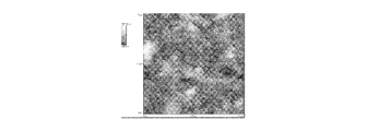
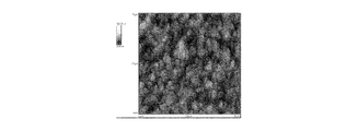
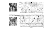
- FIG. It is a figure which shows the result of having measured the uneven
- the glass plate with a transparent conductive film shown in FIG. 1 includes a glass plate 1 and a transparent conductive film 3 formed on the glass plate 1.
- a base film 2 is interposed between the glass plate 1 and the transparent conductive film 3, and the base film 2 includes a first base layer 21 and a second base layer 22 from the glass plate 1 side. It is a film.
- the transparent conductive film 3 includes a layer 31 mainly composed of tin oxide, and an island portion 32 formed on the surface of the layer 31.
- the island part 32 is mainly composed of zinc oxide or indium oxide.
- the surface of the layer 31 is exposed from the region where the island portion 32 is not formed on the surface of the transparent conductive film 3. For this reason, on the surface of the transparent conductive film 3, there are fine convex portions (second convex portions) 33 existing on the surface of the layer 31, together with the convex portions (first convex portions) formed of the island portions 32.
- the layer 31 containing tin oxide as a main component is a polycrystalline film, and crystal grains contained in the layer 31 are exposed on the surface to form fine convex portions 33.
- the fine protrusions 33 tend to become larger as the crystal grains included in the layer 31 develop. It is known that the degree of development of crystal grains greatly depends on the film forming method of the layer 31.
- a typical film forming method in which crystal grains develop greatly is a thermal CVD method. In the case of film formation by the thermal CVD method, generally, the higher the substrate temperature (glass plate temperature) and the thicker the film, the larger the crystal grains tend to develop.
- the film formation temperature of a film containing tin oxide as a main component is usually limited to about 750 ° C. or less.
- the transparent conductive film of a thin film type solar cell is too thick, the light absorption of a film
- the film thickness of a transparent conductive film is normally restrict
- the fine convex portion 33 having almost the same size is formed.
- the size distribution of the fine protrusions 33 tends to be limited to a narrow range.
- Film formation conditions such as temperature that affect the degree of crystal grain development are factors that determine the film thickness and the like of the transparent conductive film 3, and thus greatly affect the optical and electrical characteristics of the film 3. For this reason, usually, the same film formation conditions are applied in the entire region where the transparent conductive film 3 is to be formed, and the surface shapes of the films are substantially the same. Under such circumstances, it is difficult to widen the range of the size distribution of the fine protrusions 33 formed as the crystal grains develop.
- the fine convex portion 33 on the surface of the layer 31 mainly composed of tin oxide it is not easy to grow large on the fine convex portion 33 on the surface of the layer 31 mainly composed of tin oxide, and it is not easy to widen the size distribution range. Is accompanied.
- the island part (first convex part) 32 exists on the surface of the transparent conductive film 3
- the size and distribution of the convex part on the surface of the transparent conductive film 3 are fine convex parts (second convex part). Not limited by the size of 33 and its distribution constraints.
- the first convex portion 32 is formed on the surface of the layer 31 so as to cover the second convex portion 33, has a top portion at a position relatively higher than the second convex portion 33, and the second convex portion 33.
- the larger convex part is comprised.
- the relatively large first protrusion 32 has a larger contribution to the diffusion of light having a longer wavelength than the relatively small second protrusion 33.
- the relatively large first convex portion 32 and the relatively small second convex portion 33 are present on the surface of the transparent conductive film 3, the wavelength is wider than when only one of the convex portions is present. Incident light can be effectively scattered in the region.
- the transparent conductive film 3 having two kinds of convex portions 31 and 32 on its surface basically has a structure suitable for improving the photoelectric conversion efficiency of the thin-film solar cell.
- the height of the first protrusion 32 is preferably 200 nm to 600 nm, particularly preferably 300 nm to 500 nm.
- the diameter of the first convex portion 32 is preferably 0.5 ⁇ m to 2.0 ⁇ m, particularly preferably 0.7 ⁇ m to 1.5 ⁇ m. If the first convex portion 32 is too small, a sufficient light scattering effect cannot be obtained. On the other hand, when the 1st convex part 32 is too large, the film quality of a photoelectric converting layer may deteriorate. Since the 2nd convex part 33 is very fine, it is appropriate to express the magnitude
- the surface roughness Ra of the layer 31 is preferably 10 nm to 50 nm, particularly 20 nm to 30 nm, in a region exposed on the surface of the transparent conductive film 3 (a region where the first convex portion
- the layer 31 containing tin oxide as a main component is a continuous layer formed so as to cover the lower structure (second base layer 22 in the embodiment shown in FIG. 1) existing below the transparent conductive film 3 (this specification).
- the layer covering the substructure so as not to be exposed is sometimes referred to as “continuous layer”).
- the thickness of the layer 31 is preferably 400 nm to 900 nm, more preferably 500 nm to 800 nm, and particularly preferably 600 nm to 800 nm. If the layer 31 is too thin, the conductivity required for the transparent conductive film 3 cannot be ensured. On the other hand, if the layer 31 is too thick, the decrease in the amount of light incident on the photoelectric conversion layer accompanying the increase in light absorption of the transparent conductive film 3 exceeds the effect of improving the conductivity, and the photoelectric conversion efficiency decreases.
- At least a part of the surface of the transparent conductive film 3 is covered with an island part (first convex part) 32, and a layer 31 mainly composed of tin oxide is exposed in the remaining part of the surface of the film 3.
- the islands 32 cover the surface of the layer 31 at an appropriate ratio.
- the ratio of the region D1 where the island portion 32 is formed to the region D2 where the layer 31 mainly composed of tin oxide is exposed is 80:20 to 50:50, particularly 75. : 25 to 60:40 is appropriate. This ratio can be calculated from a roughness curve measured using an atomic force microscope, as will be described later.
- the glass plate with a transparent conductive film according to the present invention is excellent in the light scattering effect from the visible long wavelength region to the near infrared region.
- This light scattering effect is expressed by a haze ratio at a wavelength of 800 nm, preferably 10% or more, more preferably 15% or more, for example, 15 to 30%.
- the haze ratio in the measurement wavelength region of 380 nm to 760 nm is preferably 30% or more, more preferably 40% or more, for example 45 to 60%.
- the light scattering effect is preferably 10% or more, for example, 15 to 20%, expressed by diffuse light transmittance at a wavelength of 800 nm.
- the conductivity of the transparent conductive film 3 may be set as appropriate based on the required characteristics of the thin film solar cell to be used, but is usually 30 ⁇ / ⁇ or less, more preferably 20 ⁇ / ⁇ or less, indicated by the sheet resistance value on the film surface. In particular, 5 to 15 ⁇ / ⁇ or less is preferable.
- a known dopant is usually added to the layer 31 containing tin oxide as a main component in order to enhance conductivity.
- the dopant for tin oxide include fluorine and antimony.
- the addition of the dopant to the island part 32 is effective in reducing the contact resistance between the transparent conductive film 3 and the photoelectric conversion layer formed thereon.
- the dopant for the island portion mainly composed of zinc oxide include boron, aluminum, gallium and indium. Tin can be exemplified as the dopant for the island portion mainly composed of indium oxide. Indium oxide doped with tin is called ITO.
- a base film 2 may be interposed between the glass plate 1 and the transparent conductive film 3.
- the base film 2 is formed as necessary for adjusting the optical characteristics of the glass plate with a transparent conductive film and for preventing the diffusion of alkali components from the glass plate 1.
- the underlayer 2 may be composed of a single layer, but may be composed of two or more layers, and is preferably composed of the first underlayer 21 and the second underlayer 22.
- the first underlayer 21 formed in contact with the glass plate 1 is preferably composed mainly of silicon oxide, titanium oxide, zinc oxide, or silicon oxycarbide, and particularly preferably composed mainly of tin oxide.
- the second underlayer 22 is preferably composed mainly of silicon oxide or aluminum oxide, and particularly preferably composed mainly of silicon oxide.
- the preferred film thickness of the first underlayer 21 is 10 nm to 100 nm, particularly 20 nm to 70 nm.
- the preferred film thickness of the second underlayer 22 is 5 nm to 80 nm, particularly 10 nm to 40 nm.
- the type of glass plate 1 is not limited, but general-purpose soda lime glass may be used.
- the thickness of the glass plate 1 is preferably 2 mm to 5 mm, for example.
- a laminate in which a layer 31 mainly composed of tin oxide is formed on a glass plate 1 is prepared.
- a base film 2 that is an arbitrary layer is interposed between the glass plate 1 and the layer 31.
- the layer 31 containing tin oxide as a main component does not need to be formed in anticipation of thickness reduction due to etching because tin oxide is excellent in etching resistance. Therefore, the layer 31 is preferably formed to have a thickness in the range exemplified above.
- a preferred film formation method for the layer 31 is a CVD method, particularly a thermal CVD method in which a raw material gas is reacted with the heat of the substrate.
- Patent Document 2 Details of a method for forming a conductive layer containing tin oxide as a main component by a thermal CVD method are disclosed in Patent Document 2, for example. On the surface of the layer 31 formed by the thermal CVD method, fine convex portions (second convex portions 33) appear as the crystal grains develop.
- a layer 35 mainly composed of zinc oxide or indium oxide is formed on the surface of the layer 31 mainly composed of tin oxide.
- the layer 35 is formed as a continuous layer covering the entire surface of the layer 31 mainly composed of tin oxide. Since the layer 35 is etched in the next step, it is referred to as an “etched layer” in this specification.
- the etched layer 35 should be formed to have a predetermined thickness determined in consideration of the thickness reduction due to etching performed in the next process and the height of the island portion to be formed.
- the thickness of the layer to be etched 35 is preferably 400 nm to 1000 nm, particularly 600 nm to 900 nm.
- the film formation method of the etching target layer 35 is not particularly limited, and may be a known film formation method represented by a sputtering method, an electron beam evaporation method, a spray pyrolysis method, or a CVD method.
- the layer 35 to be etched is, for example, an ITO layer, and, for example, a zinc oxide layer (ZnO layer, ZnO: Al layer, ZnO: Ga layer, etc.) to which aluminum, gallium, or the like is added as necessary. ).
- a zinc oxide layer ZnO layer, ZnO: Al layer, ZnO: Ga layer, etc.
- the etching target layer 35 is etched from the surface thereof. As the etching progresses, fine irregularities appear on the surface of the etched layer 35. At the stage shown in FIG. 2B, the layer to be etched 35 maintains a form as a continuous layer covering the entire surface of the layer 31 which is the lower structure. Conventionally, when light scattering characteristics should be imparted by etching, the etching process of the transparent conductive film has been stopped at the stage of maintaining the form of the layer 35 as a continuous layer (FIG. 2B). This is because if the layer 35 is divided in the in-plane direction (left-right direction in the figure), it is difficult to ensure the conductivity of the transparent conductive film.
- the etching process of the etching target layer 35 is further continued, and a part of the surface of the layer 31 containing tin oxide as a main component is exposed.
- the etching process is further performed so that the exposed surface of the layer 31 is expanded to such an extent that fine irregularities present on the surface of the layer 31 mainly composed of tin oxide can sufficiently contribute to the light scattering effect (FIG. 2). (C)).
- the layer to be etched 35 remains as islands 32 separated from each other on the surface of the layer 31 mainly composed of tin oxide. In this state, the conductivity of the transparent conductive film 3 is ensured by the layer 31 mainly composed of tin oxide.
- a continuous layer 31 that is a tin oxide layer (SnO 2 : F layer) doped with fluorine, for example, and an island portion 32 that covers a part of the surface of the layer 31 and rises upward from the surface are provided.
- a transparent conductive film 3 is formed.
- Etching may be performed according to a known method.
- acids such as hydrochloric acid, nitric acid, sulfuric acid, phosphoric acid, and acetic acid are suitable.
- An etchant such as aqua regia containing multiple acids may be used.
- Etching can be performed by wet etching using an etchant, but is not limited thereto, and may be performed by dry etching in which an etching gas is supplied to the surface of the etching target layer 35.
- an etching gas used for dry etching hydrogen halide such as hydrogen chloride is suitable.
- the etching gas is not limited to a hydrogen halide gas but may be an organic gas etching gas used in the transparent electrode patterning technology.
- the side surface of the island portion (first convex portion) 32 shown in FIG. 1 is a surface that appears by etching. As shown in the figure, this side surface has a tendency that the curve appearing in the cross section tends to approach the film surface vertical direction (up and down direction in the drawing) as it goes from the bottom to the top. In other words, the side surface of the island part 32 is a curve in which the angle with the film thickness direction of the film 3 decreases in the cross section cut along the film thickness direction of the transparent conductive film 3 from the bottom to the top of the island part 32.
- the photoelectric conversion layer formed on the transparent conductive film 3 has a smooth surface. The degree of adverse effects on characteristics is small.
- Example 1 A first underlayer (tin oxide layer: thickness 25 nm) and a second underlayer (silicon oxide layer: thickness 25 nm) are formed on a glass plate (thickness 3.2 mm) made of soda lime silica glass by a CVD method. Films were formed in this order.
- the glass plate on which the base film composed of the first base layer and the second base layer is formed is put into a substrate transport atmospheric pressure CVD apparatus, the glass plate is heated to 550 ° C., and the glass plate on which the base film is formed A mixed gas consisting of dimethyltin dichloride (DMT), water vapor, oxygen, hydrogen chloride, hydrogen fluoride and nitrogen as a carrier gas is supplied to the surface, and the thickness is 600 nm made of fluorine-doped tin oxide (SnO 2 : F) A continuous layer was deposited.
- DMT dimethyltin dichloride
- oxygen oxygen
- hydrogen chloride hydrogen fluoride
- nitrogen nitrogen
- the glass plate on which the fluorine-doped tin oxide layer was formed was put into the CVD apparatus, and the glass plate was heated to 550 ° C., and dimethyl zinc (DMZ), water vapor and carrier gas were formed on the surface of the fluorine-doped tin oxide layer.
- DMZ dimethyl zinc
- carrier gas carrier gas
- the thin film laminated glass plate was immersed in hydrochloric acid having a concentration of 0.05 mol / L for 40 seconds at room temperature to etch the zinc oxide layer (etched layer). Finally, washing with running water with city water and drying by air blowing were performed to obtain a glass plate with a transparent conductive film in which the zinc oxide layer was separated into islands and remained.
- Example 2 Except for the etching time being 10 seconds (Example 2) and 30 seconds (Example 3), a glass plate with a transparent conductive film in which the zinc oxide layer was separated into islands and remained in the same manner as in Example 1 was obtained. Obtained.
- Examples 4 and 5 Same as Example 1 except that the etching time is 30 seconds (Example 4), 40 seconds (Example 5), and the temperature of the glass plate when the zinc oxide layer is formed by the thermal CVD method is 660 ° C. Thus, a glass plate with a transparent conductive film in which the zinc oxide layer was separated and remained in an island shape was obtained.
- Example 1 A glass plate with a transparent conductive film was obtained in the same manner as in Example 1 except that the formation and etching of the zinc oxide layer were not performed. In this glass plate, only the fluorine-doped tin oxide layer is formed on the base film.
- Example 2 A glass plate with a transparent conductive film from which all of the zinc oxide layer had melted was obtained in the same manner as in Example 1 except that the etching time was set to 70 seconds.
- Comparative Examples 3, 4, 5 a thin film laminated glass plate was obtained by forming a zinc oxide layer directly on the base film without forming the fluorine-doped tin oxide layer in Example 1. Using this thin film laminated glass plate, the zinc oxide layer was etched in the same manner as in Example 1 to obtain a glass plate with a transparent conductive film. However, the etching time was 0 seconds (not etched; Comparative Example 3), 30 seconds (Comparative Example 4), and 70 seconds (Comparative Example 5).
- this average line is a line segment extending in the horizontal direction so as to intersect the roughness curve of FIG. Furthermore, using this average line as a reference, the width (distance between two intersections of the average line and the roughness curve) and height were measured for each giant convex portion (height 200 nm or more, width 0.5 ⁇ m or more).
- the measurement according to the above was carried out along two line segments each traversing this area vertically and horizontally at five square areas each having a side of 5 ⁇ m arbitrarily defined on the surface of each transparent conductive film (the total number of measurements was 10 times). Is). And the average value of the width
- the shape of the island portion observed from this direction is regarded as a circle, and the width W is regarded as the diameter D.
- the area ratio of the island portion occupying the film surface was obtained, and the ratio between the region D1 and the region D2 was calculated.
- FIGS 3 to 8 show part of the measurement data.
- the measurement results are summarized in Tables 1 and 2.
- the average roughness Ra shown in the table is a value obtained by measuring the entire transparent conductive film (a value for the entire film surface including the island part for a film in which the island part is formed).
- the glass plate with a transparent conductive film of each Example in which a transparent conductive film composed of a continuous layer and an island portion formed on this layer was formed showed a high haze ratio (Table 1), from the visible range to the near red A high diffused light transmittance was shown in a wide wavelength region extending to the outer region (FIG. 6). Although the glass plate with a transparent conductive film obtained from Comparative Example 4 showed a higher haze ratio than the other Comparative Examples, the sheet resistance value increased because the transparent conductive film was divided.
Landscapes
- Chemical & Material Sciences (AREA)
- Materials Engineering (AREA)
- Engineering & Computer Science (AREA)
- Chemical Kinetics & Catalysis (AREA)
- General Chemical & Material Sciences (AREA)
- Organic Chemistry (AREA)
- Mechanical Engineering (AREA)
- Metallurgy (AREA)
- Geochemistry & Mineralogy (AREA)
- Life Sciences & Earth Sciences (AREA)
- Inorganic Chemistry (AREA)
- Photovoltaic Devices (AREA)
- Laminated Bodies (AREA)
- Chemical Vapour Deposition (AREA)
- Non-Insulated Conductors (AREA)
- Manufacturing Of Electric Cables (AREA)
- Surface Treatment Of Glass (AREA)
Abstract
La présente invention concerne une feuille de verre avec une membrane conductrice transparente, dans laquelle une membrane conductrice transparente
(3) formée sur une feuille de verre (1) a une couche (31) qui est formée principalement d'oxyde d'étain, et une partie insulaire (32)qui est positionnée sur la surface de la couche (31)et qui est formée principalement d'oxyde d'indium ou d'oxyde de zinc, et une première partie convexe (32) comprenant la partie insulaire et une deuxième partie convexe (33) présente sur la couche de surface sont exposées sur la surface de la membrane conductrice transparente (3). La feuille de verre avec une membrane conductrice transparente a une structure adaptée pour diffuser efficacement de la lumière dans une plage de longueur d'onde large de la plage visible à la plage de l'infrarouge proche.
Applications Claiming Priority (2)
| Application Number | Priority Date | Filing Date | Title |
|---|---|---|---|
| JP2011-140156 | 2011-06-24 | ||
| JP2011140156A JP2013006735A (ja) | 2011-06-24 | 2011-06-24 | 透明導電膜付きガラス板およびその製造方法 |
Publications (1)
| Publication Number | Publication Date |
|---|---|
| WO2012176467A1 true WO2012176467A1 (fr) | 2012-12-27 |
Family
ID=47422320
Family Applications (1)
| Application Number | Title | Priority Date | Filing Date |
|---|---|---|---|
| PCT/JP2012/004055 Ceased WO2012176467A1 (fr) | 2011-06-24 | 2012-06-22 | Feuille de verre avec membrane conductrice transparente et procédé de fabrication de celle-ci |
Country Status (2)
| Country | Link |
|---|---|
| JP (1) | JP2013006735A (fr) |
| WO (1) | WO2012176467A1 (fr) |
Cited By (1)
| Publication number | Priority date | Publication date | Assignee | Title |
|---|---|---|---|---|
| JPWO2022255199A1 (fr) * | 2021-05-31 | 2022-12-08 |
Families Citing this family (2)
| Publication number | Priority date | Publication date | Assignee | Title |
|---|---|---|---|---|
| WO2015093029A1 (fr) * | 2013-12-17 | 2015-06-25 | 日本板硝子株式会社 | Procédé de fabrication de feuille de verre et feuille de verre |
| JP2021012949A (ja) * | 2019-07-05 | 2021-02-04 | Agc株式会社 | 透明電極基板及び太陽電池 |
Citations (2)
| Publication number | Priority date | Publication date | Assignee | Title |
|---|---|---|---|---|
| JP2000294812A (ja) * | 1999-04-07 | 2000-10-20 | Sanyo Electric Co Ltd | 光電変換素子及びその製造方法 |
| WO2010004811A1 (fr) * | 2008-07-07 | 2010-01-14 | 三菱電機株式会社 | Cellule solaire à couches minces et procédé de fabrication de cette cellule |
-
2011
- 2011-06-24 JP JP2011140156A patent/JP2013006735A/ja not_active Withdrawn
-
2012
- 2012-06-22 WO PCT/JP2012/004055 patent/WO2012176467A1/fr not_active Ceased
Patent Citations (2)
| Publication number | Priority date | Publication date | Assignee | Title |
|---|---|---|---|---|
| JP2000294812A (ja) * | 1999-04-07 | 2000-10-20 | Sanyo Electric Co Ltd | 光電変換素子及びその製造方法 |
| WO2010004811A1 (fr) * | 2008-07-07 | 2010-01-14 | 三菱電機株式会社 | Cellule solaire à couches minces et procédé de fabrication de cette cellule |
Cited By (2)
| Publication number | Priority date | Publication date | Assignee | Title |
|---|---|---|---|---|
| JPWO2022255199A1 (fr) * | 2021-05-31 | 2022-12-08 | ||
| WO2022255199A1 (fr) * | 2021-05-31 | 2022-12-08 | Agc株式会社 | Substrat à film stratifié |
Also Published As
| Publication number | Publication date |
|---|---|
| JP2013006735A (ja) | 2013-01-10 |
Similar Documents
| Publication | Publication Date | Title |
|---|---|---|
| JP5095776B2 (ja) | 透明導電膜付き透明基体とその製造方法、およびこの基体を含む光電変換素子 | |
| JP5012793B2 (ja) | 透明導電性酸化物膜付き基体および光電変換素子 | |
| JP5174966B2 (ja) | 薄膜太陽電池およびその製造方法 | |
| CN100595933C (zh) | 太阳能电池用透明导电性基板的制造方法 | |
| WO2002043079A1 (fr) | Film électro-conducteur, procédé de production, substrat ainsi pourvu, et convertisseur photoélectrique | |
| JP2005311292A (ja) | 薄膜太陽電池用基板、及びその製造方法、並びにそれを用いた薄膜太陽電池 | |
| JP2012028827A (ja) | 薄膜太陽電池用基板および薄膜太陽電池の製造方法 | |
| WO2002043080A1 (fr) | Film électro-conducteur transparent, procédé de fabrication et transducteur photoélectrique comprenant ce film | |
| JP2013529845A (ja) | 透明導電性酸化膜を備える基体及びその製造方法 | |
| WO2010016468A1 (fr) | Substrat à film conducteur transparent et cellule solaire utilisant le substrat | |
| JP5127925B2 (ja) | 薄膜太陽電池およびその製造方法 | |
| WO2011013775A1 (fr) | Substrat conducteur transparent pour cellules solaires et cellule solaire | |
| WO2012176467A1 (fr) | Feuille de verre avec membrane conductrice transparente et procédé de fabrication de celle-ci | |
| CN105051244B (zh) | 溅射的透明导电的铝掺杂的氧化锌膜 | |
| JP5502412B2 (ja) | 光起電力装置の製造方法 | |
| JPWO2012169602A1 (ja) | 透明導電膜付き基板 | |
| WO2011121922A1 (fr) | Plaque de verre comportant un film conducteur transparent et procédé pour fabriquer la plaque de verre | |
| JP4362273B2 (ja) | 基板の製造方法 | |
| JP2001015787A (ja) | 透明導電膜付き基体、その製造方法および太陽電池 | |
| JP2012084843A (ja) | 透明導電性酸化物膜付き基体、および光電変換素子 | |
| JP5650057B2 (ja) | 透明電極基板、及びその製造方法 | |
| JP2014038807A (ja) | 透明導電性酸化物膜付き基体およびその製造方法 | |
| JP2002158366A (ja) | 光電変換装置 | |
| JP2009239301A (ja) | 基板およびそれを用いた光電変換装置 | |
| JP2012132048A (ja) | 透明導電膜付き基体 |
Legal Events
| Date | Code | Title | Description |
|---|---|---|---|
| 121 | Ep: the epo has been informed by wipo that ep was designated in this application |
Ref document number: 12802767 Country of ref document: EP Kind code of ref document: A1 |
|
| NENP | Non-entry into the national phase |
Ref country code: DE |
|
| 122 | Ep: pct application non-entry in european phase |
Ref document number: 12802767 Country of ref document: EP Kind code of ref document: A1 |