WO2013018485A1 - Grille de connexion, procédé de fabrication d'une grille de connexion et dispositif semi-conducteur l'utilisant - Google Patents
Grille de connexion, procédé de fabrication d'une grille de connexion et dispositif semi-conducteur l'utilisant Download PDFInfo
- Publication number
- WO2013018485A1 WO2013018485A1 PCT/JP2012/066958 JP2012066958W WO2013018485A1 WO 2013018485 A1 WO2013018485 A1 WO 2013018485A1 JP 2012066958 W JP2012066958 W JP 2012066958W WO 2013018485 A1 WO2013018485 A1 WO 2013018485A1
- Authority
- WO
- WIPO (PCT)
- Prior art keywords
- die pad
- lead frame
- semiconductor device
- burr
- metal burr
- Prior art date
- Legal status (The legal status is an assumption and is not a legal conclusion. Google has not performed a legal analysis and makes no representation as to the accuracy of the status listed.)
- Ceased
Links
Images


Classifications
-
- H—ELECTRICITY
- H10—SEMICONDUCTOR DEVICES; ELECTRIC SOLID-STATE DEVICES NOT OTHERWISE PROVIDED FOR
- H10W—GENERIC PACKAGES, INTERCONNECTIONS, CONNECTORS OR OTHER CONSTRUCTIONAL DETAILS OF DEVICES COVERED BY CLASS H10
- H10W70/00—Package substrates; Interposers; Redistribution layers [RDL]
- H10W70/40—Leadframes
- H10W70/411—Chip-supporting parts, e.g. die pads
- H10W70/415—Leadframe inner leads serving as die pads
-
- H—ELECTRICITY
- H10—SEMICONDUCTOR DEVICES; ELECTRIC SOLID-STATE DEVICES NOT OTHERWISE PROVIDED FOR
- H10W—GENERIC PACKAGES, INTERCONNECTIONS, CONNECTORS OR OTHER CONSTRUCTIONAL DETAILS OF DEVICES COVERED BY CLASS H10
- H10W70/00—Package substrates; Interposers; Redistribution layers [RDL]
- H10W70/01—Manufacture or treatment
- H10W70/04—Manufacture or treatment of leadframes
- H10W70/048—Mechanical treatments, e.g. punching, cutting, deforming or cold welding
-
- H—ELECTRICITY
- H10—SEMICONDUCTOR DEVICES; ELECTRIC SOLID-STATE DEVICES NOT OTHERWISE PROVIDED FOR
- H10W—GENERIC PACKAGES, INTERCONNECTIONS, CONNECTORS OR OTHER CONSTRUCTIONAL DETAILS OF DEVICES COVERED BY CLASS H10
- H10W70/00—Package substrates; Interposers; Redistribution layers [RDL]
- H10W70/40—Leadframes
- H10W70/411—Chip-supporting parts, e.g. die pads
-
- H—ELECTRICITY
- H10—SEMICONDUCTOR DEVICES; ELECTRIC SOLID-STATE DEVICES NOT OTHERWISE PROVIDED FOR
- H10W—GENERIC PACKAGES, INTERCONNECTIONS, CONNECTORS OR OTHER CONSTRUCTIONAL DETAILS OF DEVICES COVERED BY CLASS H10
- H10W70/00—Package substrates; Interposers; Redistribution layers [RDL]
- H10W70/40—Leadframes
- H10W70/421—Shapes or dispositions
- H10W70/424—Cross-sectional shapes
-
- H—ELECTRICITY
- H10—SEMICONDUCTOR DEVICES; ELECTRIC SOLID-STATE DEVICES NOT OTHERWISE PROVIDED FOR
- H10W—GENERIC PACKAGES, INTERCONNECTIONS, CONNECTORS OR OTHER CONSTRUCTIONAL DETAILS OF DEVICES COVERED BY CLASS H10
- H10W72/00—Interconnections or connectors in packages
- H10W72/01—Manufacture or treatment
- H10W72/019—Manufacture or treatment of bond pads
-
- H—ELECTRICITY
- H10—SEMICONDUCTOR DEVICES; ELECTRIC SOLID-STATE DEVICES NOT OTHERWISE PROVIDED FOR
- H10W—GENERIC PACKAGES, INTERCONNECTIONS, CONNECTORS OR OTHER CONSTRUCTIONAL DETAILS OF DEVICES COVERED BY CLASS H10
- H10W74/00—Encapsulations, e.g. protective coatings
- H10W74/10—Encapsulations, e.g. protective coatings characterised by their shape or disposition
- H10W74/111—Encapsulations, e.g. protective coatings characterised by their shape or disposition the semiconductor body being completely enclosed
-
- H—ELECTRICITY
- H10—SEMICONDUCTOR DEVICES; ELECTRIC SOLID-STATE DEVICES NOT OTHERWISE PROVIDED FOR
- H10W—GENERIC PACKAGES, INTERCONNECTIONS, CONNECTORS OR OTHER CONSTRUCTIONAL DETAILS OF DEVICES COVERED BY CLASS H10
- H10W74/00—Encapsulations, e.g. protective coatings
-
- H—ELECTRICITY
- H10—SEMICONDUCTOR DEVICES; ELECTRIC SOLID-STATE DEVICES NOT OTHERWISE PROVIDED FOR
- H10W—GENERIC PACKAGES, INTERCONNECTIONS, CONNECTORS OR OTHER CONSTRUCTIONAL DETAILS OF DEVICES COVERED BY CLASS H10
- H10W90/00—Package configurations
- H10W90/701—Package configurations characterised by the relative positions of pads or connectors relative to package parts
- H10W90/751—Package configurations characterised by the relative positions of pads or connectors relative to package parts of bond wires
- H10W90/756—Package configurations characterised by the relative positions of pads or connectors relative to package parts of bond wires between a chip and a stacked lead frame, conducting package substrate or heat sink
Definitions
- the present invention relates to a lead frame in which a lower surface of a die pad is exposed, a manufacturing method of the lead frame, and a semiconductor device using the same.
- Semiconductor elements are used not only for information and signal processing, but also for current and power control of electrical circuits and electronic circuits.
- a semiconductor element used for controlling such current and power consumes a larger current and voltage (power) than a semiconductor element used for information and signal processing. Called an element.
- a semiconductor device also referred to as a semiconductor package
- a semiconductor package incorporating such a power element generates a large amount of heat because a high current flows through the semiconductor device and operates under a high voltage. Therefore, in order to release the heat generated in the chip (semiconductor element) inside the semiconductor device to the outside, a heat spreader is inserted or a heat slug is attached to the exposed surface of the die pad.
- a heat spreader is inserted or a heat slug is attached to the exposed surface of the die pad.
- it has been attempted to radiate heat directly from the heat radiating surface formed by exposing the lower surface of the die pad to the outside of the semiconductor device.
- the lower surface of the die pad is pressed against a resin mold to inject sealing resin, and the lower surface of the die pad is exposed from the package to form an exposed surface.
- the sealing resin may flow from the gap between the lower surface of the die pad and the resin molding die.
- an unintended sealing resin is injected into the boundary between the exposed surface of the die pad and the portion covered with the sealing resin to form a resin burr.
- Such a resin burr has covered a part or all of the exposed surface of the die pad used as a heat release passage, and has been a cause of reducing heat dissipation.
- Patent Document 1 a ring-shaped groove is formed on the exposed surface of the die pad.
- the sealing resin that has entered between the exposed surface of the die pad and the resin mold during injection of the sealing resin flows into this groove, and the sealing resin enters the exposed surface of the die pad beyond the groove. Is preventing.
- a protruding wall is formed around the exposed surface of the die pad by pressing the exposed surface of the die pad with a punch. This protruding wall prevents the sealing resin from entering the exposed surface of the die pad inside the protruding wall.
- a protruding wall is formed around the exposed surface of the die pad to prevent the sealing resin from entering.
- a space for filling the sealing resin is formed between the die pad and the resin molding die at the time of resin sealing. It cannot be pressed directly with the upper mold of the resin mold. For this reason, when there is a slight variation in the height of the protruding wall, there is a problem that the resin enters through the gap between the protruding walls and a thick resin burr is formed inside the protruding wall on the exposed surface of the die pad.
- the die pad 70 is partially pushed up by the encapsulating sealing resin 77, and the sealing resin 77 is in a state where the die pad 70 is tilted. It may harden. At this time, a thick resin burr 73 is formed on a part of the exposed surface of the die pad 70.
- reference numeral 74 denotes a semiconductor element
- 75 and 76 denote leads
- 78 denotes an upper mold.
- the resin burr 73 is also generated by the techniques of Patent Document 1 and Patent Document 2.
- the heat dissipation of the semiconductor device may be reduced. Therefore, when the resin burr 73 is generated, the semiconductor device 80 is immersed in a solution that makes the resin burr 73 easy to peel off for a predetermined time, and then a high water pressure water flow is applied to the resin burr 73 to remove the resin burr 73. Yes.
- the semiconductor device 80 is placed in a solution that makes it easy to peel off the resin burr 73 after the resin burr 73 is irradiated with a laser after the resin molding to carbonize the resin burr 73.
- the resin burr 73 is removed by immersion for a long time and further with a high water pressure water flow. Such a process is performed as a pretreatment for the exterior plating process.
- the resin burr 73 when the resin burr 73 is formed thick or the area of the resin burr 73 is large, it takes a long time for laser irradiation or a long time for immersion in the solution, which increases the manufacturing cost. . Further, not only the resin burr 73 but also the sealing resin 77 that seals the lead frame 81 is peeled off by such a process, and the function of the semiconductor device 80 as a product may be impaired.
- the present invention has been made in view of such circumstances, and an object of the present invention is to provide a semiconductor device in which a die pad is easily exposed and has good heat dissipation, a lead frame used in the semiconductor device, and a method of manufacturing the lead frame.
- a semiconductor device has a die pad mounted on an upper surface, and a lead frame used in a semiconductor device in a state where the lower surface of the die pad is exposed from a sealing resin, On the lower surface of the die pad, a first metal burr projecting downward is formed on the outer periphery thereof, The tip of the first metal burr is flat.
- a plurality of external terminals provided around the die pad;
- the lower surface of the external terminal is flush with the lower surface of the die pad,
- a second metal burr protruding downward is formed on the outer periphery thereof,
- the tip of the second metal burr may be flat.
- the height of the first metal burr is preferably greater than 0 ⁇ m and not greater than 10 ⁇ m.
- a method of manufacturing a lead frame according to the present invention that meets the above-described object is as follows.
- a semiconductor device has a die pad mounted on an upper surface, and a manufacturing method of a lead frame used in a semiconductor device in a state where a lower surface of the die pad is exposed from a sealing resin,
- the tip of the first metal burr which is formed when the die pad is punched from the metal plate and projects downwardly on the outer peripheral portion of the lower surface of the die pad, is pressed with a punch to flatten the tip of the first metal burr It is characterized by.
- a plurality of external terminals having a lower surface that is flush with the lower surface of the die pad are formed at the outer peripheral portion of the lower surface of each external terminal formed when the metal plate is punched out so as to be formed around the die pad.
- the tip of the second metal burr that protrudes downward may be pressed with a punch, and the tip of the second metal burr may be flat.
- a semiconductor device that meets the above-mentioned object is as follows.
- a semiconductor element A lead frame provided with a die pad on which the semiconductor element is mounted; Sealing resin for sealing the semiconductor element together with the lead frame, The lower surface of the die pad is exposed to the outside from the sealing resin, On the lower surface of the die pad, a first metal burr projecting downward is formed on the outer periphery thereof, The tip of the first metal burr is flat.
- the lead frame has a plurality of external terminals provided around the die pad, The lower surface of the external terminal is flush with the lower surface of the die pad, On the lower surface of each of the external terminals, a second metal burr protruding downward is formed on the outer periphery thereof, The tip of the second metal burr may be flat.
- the first metal burr is formed on the outer peripheral portion of the exposed surface of the die pad, when the lead frame and the semiconductor element are sealed with the sealing resin.
- the first metal burr can suppress the sealing resin from entering the exposed surface side of the die pad.
- the tip of the first metal burr is flat, the contact area where the first metal burr contacts the lower mold in the resin sealing process is increased, and the sealing resin is on the exposed surface side of the die pad. Can be prevented from entering. Therefore, resin burrs are hardly formed, and the formed resin burrs are small and easy to remove. For this reason, the exposed surface of the die pad is easily exposed, and a semiconductor device excellent in heat dissipation and a lead frame used therefor can be provided.
- the tip of the first metal burr formed when the lead frame is punched out from the metal plate is made flat. Therefore, generation
- FIG. 6 is a rear view of a part of the lead frame.
- FIG. 2 is a side sectional view of the semiconductor device shown in FIG. 1.
- (A) And (B) is a figure which shows the manufacturing process of a lead frame. It is a side view of a part of a lead frame. It is the elements on larger scale of the exposed surface of a lead frame. It is a sectional side view of the semiconductor device which concerns on the modification of this invention.
- FIG. 8 is a partial enlarged view of the semiconductor device shown in FIG. 7.
- A) is sectional drawing of the semiconductor device which concerns on a prior art example
- (B) is a partially expanded sectional view of the semiconductor device.
- (A) is sectional drawing of the semiconductor device which concerns on a prior art example
- (B) is a bottom view of the die pad of the semiconductor device.
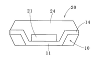
- FIG. 1 is a bottom view of a semiconductor device 20 according to an embodiment of the present invention.
- the semiconductor device 20 includes a semiconductor element 21, a lead frame 10 on which the semiconductor element 21 is mounted, and a sealing resin 24 that seals the semiconductor element 21 and the lead frame 10 together.
- the lead 13 and the semiconductor element 21 are electrically connected by a bonding wire (not shown).
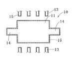
- FIG. 2 is a rear view of the lead frame 10.
- the lead frame 10 includes a die pad 11 on which a semiconductor element 21 is mounted, a support lead 14 that extends laterally from the die pad 11, and a lead 13 that extends outward from the die pad 11.
- the die pad 11 (and the support lead 14) and the lead 13 are connected to a single metal plate by a connecting portion (not shown). Further, a plurality of die pads 11 and the like may be formed on one metal plate.
- the hatched area indicates an area where a metal burr 15 described later is formed.
- FIG. 3 is a cross-sectional view of the semiconductor device 20 shown in FIG.
- the upper surface of the die pad 11 is a mounting surface, and the semiconductor element 21 is mounted on this mounting surface.
- the lower surface of the die pad 11 is an exposed surface and is exposed to the outside from the sealing resin 24. Thereby, the heat generated in the semiconductor element 21 is efficiently released to the outside through the exposed surface.
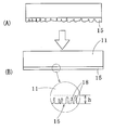
- FIG. 4 is a diagram illustrating a manufacturing process of the lead frame 10.
- 4A shows the lead frame 10 after punching a metal plate
- FIG. 4B shows the lead frame 10 after crushing with a flat punch.
- the lead frame 10 is formed into a desired shape including the die pad 11, the support lead 14, and the lead 13 by punching a metal plate using a punch and a die.
- a metal plate a thin plate member made of copper or a copper alloy can be used.
- the punch and die are arranged so that a clearance of about 1 to 10 ⁇ m is formed between them. For this reason, when the metal plate is punched, as shown in FIG. 2, the portion entering the clearance is ductile broken to form a metal burr (first metal burr) 15. When the die is fixed and the punch is moved from the upper side to the lower side, as shown in FIG. 4, a metal burr 15 extending downward of the lead frame 10 along the moving direction of the punch is formed.
- the die and the punch are formed in a shape corresponding to the desired shape.
- the clearance formed between both is also a shape corresponding to the contour of a desired shape. Therefore, as shown in FIG. 2, the metal burr 15 is formed on the outer periphery of the lead frame 10, that is, on the outer peripheral portion of each exposed surface of the die pad 11, the lead 13, and the support lead 14.
- the height dimension (vertical dimension) of the metal burr 15 in this process is 5 ⁇ m or more and 25 ⁇ m or less.
- the height dimension of the metal burr 15 can be adjusted by adjusting the clearance between the punch and the die. Note that the tip of the metal burr 15 in this state has an uneven shape.
- the tip of the metal burr 15 is crushed by a flat punch having a flat surface formed at the tip.
- the height h of the metal burr 15 is reduced, and the tip is crushed flat. It is preferable to crush so that the height h of the metal burr 15 after crushing exceeds 0 ⁇ m and is 10 ⁇ m or less, more preferably 3 ⁇ m or less.
- the metal burr 15 is pushed with a flat punch having a tip surface larger than the die pad 11 so that the tip of the entire metal burr 15 formed along the outer periphery of the die pad 11 can be pressed at once with a single flat surface. It is preferable to crush. Thereby, the height h of the metal burr
- the metal burr 15 is a part of the metal plate that has been ductile fractured by a punch and a die, and a gap 18 extending in the vertical direction may be formed in this process. However, in the process of crushing the metal burr 15, the gap 18 is also closed or reduced.
- the lead frame 10 formed with the die pad 11, the support lead 14, and the lead 13 connected to the metal plate via a connecting portion (not shown) is formed.
- the semiconductor device 20 is formed as follows. First, the lead 13 and the die pad 11 are separated from the metal plate of the lead frame 10, and the die pad 11 is further pressed down to deform the lead frame 10 into the shape shown in FIG.
- the semiconductor element 21 is fixed on the die pad 11 of the lead frame 10, and the semiconductor element 21 and each lead 13 are connected by a bonding wire (not shown) to obtain an intermediate product. Thereafter, the intermediate product is put between a lower mold and an upper mold (not shown) for resin sealing, and resin sealing is performed, whereby the semiconductor device 20 is completed.
- the metal burr 15 provided on the outer periphery of the die pad 11 is the sealing resin 24.
- the flow to the center part side of the die pad 11 can be suppressed.
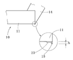
- FIG. 5 is an enlarged side sectional view showing the exposed surface of the die pad 11 of the lead frame 10.
- a thin resin burr 23 having a small area is formed on the outer peripheral portion of the exposed surface of the die pad 11, and a part of the resin burr 23 is formed.
- the exposed surface of the die pad 11 is exposed unevenly. Further, the resin burr 23 is formed only in a narrow region along the metal burr 15.
- the resin burr 23 is formed along the metal burr 15 formed along the outer periphery of the die pad 11. For this reason, even if the resin burr 23 is not removed, the heat dissipation of the semiconductor element 21 is hardly adversely affected.
- the metal burr 15 is formed to extend downward. That is, the metal burr 15 extends on the exposed surface side of the die pad 11.
- the entire lead frame 10 is curved so that the outer peripheral portion protrudes downward from the central portion. For this reason, when the lead frame 10 is arranged in the mold for resin sealing, the outer peripheral portion is pressed more strongly against the surface of the lower mold for resin sealing than the central portion of the die pad 11. For this reason, since the tip of the metal burr 15 is in close contact with the surface of the lower mold, the sealing resin 24 can be prevented from entering the exposed surface of the die pad 11.
- the tip of the metal burr 15 is flattened by flat punching after the metal burr 15 is formed by punching, the tip of the metal burr 15 is formed in the resin sealing process.
- the contact area with the lower mold surface becomes larger, and the sealing resin 24 can be prevented from entering the exposed surface side of the die pad 11.
- the height h of the metal burr 15 is lowered by pressing the tip of the metal burr 15 with a flat punch. For this reason, when the lead frame 10 is arranged in a mold for resin sealing, the height of the space formed between the exposed surface of the die pad 11 and the lower mold is also reduced. For this reason, even when the sealing resin enters the space, the thickness of the formed resin burr 23 is reduced. At this time, the height h of the metal burr 15 is preferably greater than 0 ⁇ m and not greater than 10 ⁇ m.
- the tip of the metal burr 15 formed when the lead frame 10 is punched from the metal plate is flattened, and the semiconductor device 20 is utilized using the metal burr 15.
- the generation of the resin burr 23 at the time of manufacturing is suppressed. Therefore, by effectively utilizing the metal burrs that are inevitably generated during the punching process, it is possible to provide the lead frame 10 whose exposed surface is easily exposed when used in the semiconductor device 20 at a low cost. Further, the lead frame 10 can be manufactured by a simple process of crushing the tip of the metal burr with a flat punch.
- the tip of the metal burr 15 is flattened with a flat punch, it is preferable that the height h of the metal burr 15 is made uniform. Thereby, in the resin sealing process, when the lead frame 10 is disposed in the resin sealing mold, the lead frame 10 does not rattle, and the tip of the entire metal burr 15 contacts the surface of the lower mold. For this reason, it is possible to effectively suppress the sealing resin 24 from entering the exposed surface of the die pad 11.
- a gap 18 may be generated in the metal burr 15.
- the gap 18 in the metal burr 15 is ideally closed by a pressing process using a flat punch. However, even if the gap 18 is not blocked, the metal burr 15 is deformed so that the gap 18 is reduced in the pressing process using the flat punch.
- FIG. 6 is an enlarged view showing the corner of the exposed surface of the die pad 11 of the semiconductor device 20.
- the gap 18 of the metal burr 15 is small, the amount of the sealing resin 24 flowing from the gap 18 to the exposed surface side of the die pad 11 is small. For this reason, the formed resin burr 23 is thin and small. For this reason, since the resin burr
- the exposed surface of the die pad 11 is subjected to exterior plating with a thickness of 5 to 18 ⁇ m, and the exposed surface of the die pad 11 is mounted on the substrate with solder having a height of 50 to 150 ⁇ m.
- solder having a height of 50 to 150 ⁇ m.
- each lead protruded from the lateral surface of the semiconductor device.
- the present invention can also be applied to a semiconductor device in which a terminal (external connection terminal) is exposed from the bottom surface of the semiconductor device. .
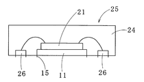
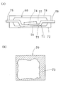
- FIG. 7 is a cross-sectional view of a semiconductor device 25 according to a modification of the present invention
- FIG. 8 is an enlarged view of the lower surface of the external terminal 26 of the semiconductor device 25.
- the semiconductor device 25 includes a plurality of external terminals 26 around the die pad 11. The lower surface of the external terminal 26 is located on the same plane as the exposed surface of the die pad 11.
- the metal burr 15 is formed on the exposed surface of the die pad 11 as described above, and the tip is pushed by a punch on the outer peripheral portion of the lower surface of the external terminal 26 as well as the metal burr 15.
- a metal burr (second metal burr) 27 that is crushed and flattened is formed. Also in such a semiconductor device 25, the resin burr formed on the lower surface of the external terminal 26 can be easily peeled off during resin sealing.
- the height of the metal burr 27 is preferably greater than 0 ⁇ m and not greater than 10 ⁇ m so that the height h is the same as the metal burr 15. Thereby, it is difficult for the sealing resin to enter the exposed surface of the die pad 11 and the lower surface of the external terminal 26.
- the first metal burr is formed on the outer peripheral portion of the exposed surface of the die pad, when the lead frame and the semiconductor element are sealed with the sealing resin.
- the first metal burr can suppress the sealing resin from entering the exposed surface side of the die pad.
- the tip of the first metal burr is flat, the contact area where the first metal burr contacts the lower mold in the resin sealing process is increased, and the sealing resin is on the exposed surface side of the die pad. Can be prevented from entering. Therefore, resin burrs are hardly formed, and the formed resin burrs are small and easy to remove. For this reason, the exposed surface of the die pad is easily exposed, and a semiconductor device excellent in heat dissipation and a lead frame used therefor can be provided.
Landscapes
- Lead Frames For Integrated Circuits (AREA)
- Encapsulation Of And Coatings For Semiconductor Or Solid State Devices (AREA)
- Engineering & Computer Science (AREA)
- Manufacturing & Machinery (AREA)
- Physics & Mathematics (AREA)
- Geometry (AREA)
Abstract
L'invention concerne une grille de connexion (10), une pastille de puce (11) pouvant être facilement exposée quand la grille de connexion (10) est utilisée pour un dispositif semi-conducteur (20). La grille de connexion (10) a une pastille de puce (11) comportant une surface supérieure sur laquelle est monté un élément semi-conducteur (21). La grille de connexion est utilisée pour le dispositif semi-conducteur (20), la surface exposée de la pastille de puce (11) étant exposée depuis une résine d'étanchéité (24). Une première barbe de métal (15) se projetant vers le bas est formée le long de la partie périphérique de la surface exposée de la pastille de puce (11) et l'extrémité de la première barbe de métal (15) est plate.
Priority Applications (2)
| Application Number | Priority Date | Filing Date | Title |
|---|---|---|---|
| US14/236,168 US9147646B2 (en) | 2011-08-01 | 2012-07-03 | Lead frame, method for manufacturing lead frame and semiconductor device using same |
| CN201280038284.2A CN103718291B (zh) | 2011-08-01 | 2012-07-03 | 引线框、引线框的制造方法和使用该引线框的半导体装置 |
Applications Claiming Priority (2)
| Application Number | Priority Date | Filing Date | Title |
|---|---|---|---|
| JP2011-168599 | 2011-08-01 | ||
| JP2011168599A JP5940257B2 (ja) | 2011-08-01 | 2011-08-01 | リードフレーム及びリードフレームの製造方法並びにこれを用いた半導体装置 |
Publications (1)
| Publication Number | Publication Date |
|---|---|
| WO2013018485A1 true WO2013018485A1 (fr) | 2013-02-07 |
Family
ID=47629017
Family Applications (1)
| Application Number | Title | Priority Date | Filing Date |
|---|---|---|---|
| PCT/JP2012/066958 Ceased WO2013018485A1 (fr) | 2011-08-01 | 2012-07-03 | Grille de connexion, procédé de fabrication d'une grille de connexion et dispositif semi-conducteur l'utilisant |
Country Status (4)
| Country | Link |
|---|---|
| US (1) | US9147646B2 (fr) |
| JP (1) | JP5940257B2 (fr) |
| CN (1) | CN103718291B (fr) |
| WO (1) | WO2013018485A1 (fr) |
Families Citing this family (3)
| Publication number | Priority date | Publication date | Assignee | Title |
|---|---|---|---|---|
| US8956920B2 (en) * | 2012-06-01 | 2015-02-17 | Nxp B.V. | Leadframe for integrated circuit die packaging in a molded package and a method for preparing such a leadframe |
| JP6266219B2 (ja) * | 2013-03-18 | 2018-01-24 | ルネサスエレクトロニクス株式会社 | 半導体装置 |
| IT202300017793A1 (it) * | 2023-08-30 | 2025-03-02 | St Microelectronics Int Nv | Procedimento per fabbricare dispositivi a semiconduttore e dispositivo a semiconduttore corrispondente |
Citations (3)
| Publication number | Priority date | Publication date | Assignee | Title |
|---|---|---|---|---|
| JPH0410346U (fr) * | 1990-05-16 | 1992-01-29 | ||
| JPH0794635A (ja) * | 1993-09-23 | 1995-04-07 | Toyota Autom Loom Works Ltd | 樹脂封止パッケージ |
| JP2011091145A (ja) * | 2009-10-21 | 2011-05-06 | Sanyo Electric Co Ltd | 半導体装置及びその製造方法 |
Family Cites Families (24)
| Publication number | Priority date | Publication date | Assignee | Title |
|---|---|---|---|---|
| US5167794A (en) * | 1990-04-16 | 1992-12-01 | Mitsubishi Denki Kabushiki Kaisha | Method for producing lead frame material |
| JPH0410346A (ja) | 1990-04-26 | 1992-01-14 | Nissin Electric Co Ltd | イオン注入装置 |
| US5227421A (en) | 1990-05-01 | 1993-07-13 | Nippon Paint Co., Ltd. | Aqueous pigment-dispersed paste, processes for producing it and therefrom water paint composition |
| JPH0697340A (ja) * | 1991-12-24 | 1994-04-08 | Mitsui High Tec Inc | リードフレームの製造方法 |
| JPH05267385A (ja) * | 1992-03-17 | 1993-10-15 | Rohm Co Ltd | ワイヤーボンディング装置 |
| US5558267A (en) * | 1995-03-31 | 1996-09-24 | Texas Instruments Incorporated | Moat for die pad cavity in bond station heater block |
| JP3405030B2 (ja) * | 1995-12-19 | 2003-05-12 | 松下電器産業株式会社 | マイクロ波用磁性体材料の製造方法、およびこれを用いた高周波回路部品 |
| JPH0927579A (ja) * | 1995-07-10 | 1997-01-28 | Apic Yamada Kk | リードフレーム製造装置 |
| US5767480A (en) * | 1995-07-28 | 1998-06-16 | National Semiconductor Corporation | Hole generation and lead forming for integrated circuit lead frames using laser machining |
| JP3885321B2 (ja) * | 1997-11-19 | 2007-02-21 | 株式会社デンソー | 樹脂封止型半導体部品の製造方法 |
| JP3510841B2 (ja) * | 2000-05-09 | 2004-03-29 | 三洋電機株式会社 | 板状体、リードフレームおよび半導体装置の製造方法 |
| JP3883784B2 (ja) * | 2000-05-24 | 2007-02-21 | 三洋電機株式会社 | 板状体および半導体装置の製造方法 |
| JP3650001B2 (ja) * | 2000-07-05 | 2005-05-18 | 三洋電機株式会社 | 半導体装置およびその製造方法 |
| JP2003124420A (ja) * | 2001-10-16 | 2003-04-25 | Shinko Electric Ind Co Ltd | リードフレーム及び該リードフレームを用いた半導体装置の製造方法 |
| TW533566B (en) * | 2002-01-31 | 2003-05-21 | Siliconware Precision Industries Co Ltd | Short-prevented lead frame and method for fabricating semiconductor package with the same |
| US7122884B2 (en) * | 2002-04-16 | 2006-10-17 | Fairchild Semiconductor Corporation | Robust leaded molded packages and methods for forming the same |
| JP2005159103A (ja) * | 2003-11-27 | 2005-06-16 | Renesas Technology Corp | 半導体装置およびその製造方法 |
| JP2006135100A (ja) | 2004-11-05 | 2006-05-25 | Matsushita Electric Ind Co Ltd | 半導体装置及びその製造方法 |
| KR100723493B1 (ko) * | 2005-07-18 | 2007-06-04 | 삼성전자주식회사 | 와이어 본딩 및 플립 칩 본딩이 가능한 스마트 카드 모듈기판 및 이를 포함하는 스마트 카드 모듈 |
| KR101089449B1 (ko) * | 2005-08-10 | 2011-12-07 | 가부시키가이샤 미츠이하이테크 | 반도체 장치 및 그 제조 방법 |
| JP2008270661A (ja) | 2007-04-24 | 2008-11-06 | Mitsui High Tec Inc | リードフレームおよびリードフレームの製造方法ならびに半導体装置および半導体装置の製造方法 |
| JP5149854B2 (ja) * | 2009-03-31 | 2013-02-20 | ルネサスエレクトロニクス株式会社 | 半導体装置 |
| DE112012005920B4 (de) * | 2012-02-22 | 2022-03-24 | Mitsubishi Electric Corporation | Halbleitervorrichtung und Verfahren zur Herstellung einer Halbleitervorrichtung |
| US8956920B2 (en) * | 2012-06-01 | 2015-02-17 | Nxp B.V. | Leadframe for integrated circuit die packaging in a molded package and a method for preparing such a leadframe |
-
2011
- 2011-08-01 JP JP2011168599A patent/JP5940257B2/ja active Active
-
2012
- 2012-07-03 US US14/236,168 patent/US9147646B2/en active Active
- 2012-07-03 CN CN201280038284.2A patent/CN103718291B/zh active Active
- 2012-07-03 WO PCT/JP2012/066958 patent/WO2013018485A1/fr not_active Ceased
Patent Citations (3)
| Publication number | Priority date | Publication date | Assignee | Title |
|---|---|---|---|---|
| JPH0410346U (fr) * | 1990-05-16 | 1992-01-29 | ||
| JPH0794635A (ja) * | 1993-09-23 | 1995-04-07 | Toyota Autom Loom Works Ltd | 樹脂封止パッケージ |
| JP2011091145A (ja) * | 2009-10-21 | 2011-05-06 | Sanyo Electric Co Ltd | 半導体装置及びその製造方法 |
Also Published As
| Publication number | Publication date |
|---|---|
| CN103718291B (zh) | 2017-03-15 |
| US20140159221A1 (en) | 2014-06-12 |
| JP2013033822A (ja) | 2013-02-14 |
| JP5940257B2 (ja) | 2016-06-29 |
| CN103718291A (zh) | 2014-04-09 |
| US9147646B2 (en) | 2015-09-29 |
Similar Documents
| Publication | Publication Date | Title |
|---|---|---|
| EP3128550B1 (fr) | Dispositif semi-conducteur | |
| EP3428962B1 (fr) | Dispositif à semi-conducteurs et procédé de fabrication de dispositif à semi-conducteurs | |
| CN105047635A (zh) | 附带散热板的引脚框架及其制造方法、以及半导体装置及其制造方法 | |
| WO2013018485A1 (fr) | Grille de connexion, procédé de fabrication d'une grille de connexion et dispositif semi-conducteur l'utilisant | |
| JP2009071154A (ja) | 半導体装置 | |
| JP2010021251A (ja) | 半導体装置及びその製造方法 | |
| JP2008270661A (ja) | リードフレームおよびリードフレームの製造方法ならびに半導体装置および半導体装置の製造方法 | |
| CN102044445B (zh) | 无外引脚半导体封装构造的导线架制造方法 | |
| JP5561072B2 (ja) | 半導体装置の製造方法 | |
| JP5112972B2 (ja) | 半導体装置およびその製造方法 | |
| JP6869602B2 (ja) | 半導体装置 | |
| JP2007036013A (ja) | 回路装置およびその製造方法 | |
| CN102148165A (zh) | 功率半导体模块的制造方法及其壳体部分的制造方法 | |
| CN106409694B (zh) | 半导体装置及其制造方法 | |
| JP2013175795A (ja) | リードフレームの製造方法 | |
| JP2013175795A5 (fr) | ||
| JP6407042B2 (ja) | 半導体装置及びその製造方法 | |
| JP5167543B2 (ja) | 放熱板付きリードフレームおよびその製造方法 | |
| JP2004127962A (ja) | 半導体装置の樹脂封止方法 | |
| JP2012004605A (ja) | リードフレームおよびリードフレームの製造方法ならびに半導体装置および半導体装置の製造方法 | |
| JPH11163056A (ja) | テープキャリアの製造方法 | |
| JP2018056310A (ja) | 樹脂封止金型およびそれを用いた半導体装置の製造方法 | |
| JP5772306B2 (ja) | モールドパッケージの製造方法 | |
| JP2005158778A (ja) | リードフレームの製造方法及び半導体装置の製造方法 | |
| KR20030079170A (ko) | 리드프레임 및, 그것을 이용한 반도체 패키지 제조 방법 |
Legal Events
| Date | Code | Title | Description |
|---|---|---|---|
| 121 | Ep: the epo has been informed by wipo that ep was designated in this application |
Ref document number: 12820782 Country of ref document: EP Kind code of ref document: A1 |
|
| WWE | Wipo information: entry into national phase |
Ref document number: 14236168 Country of ref document: US |
|
| NENP | Non-entry into the national phase |
Ref country code: DE |
|
| 122 | Ep: pct application non-entry in european phase |
Ref document number: 12820782 Country of ref document: EP Kind code of ref document: A1 |