WO2013018698A1 - Procédé de fabrication pour l'assemblage d'un panneau tactile de type capacitif et dispositif d'affichage équipé de celui-ci - Google Patents
Procédé de fabrication pour l'assemblage d'un panneau tactile de type capacitif et dispositif d'affichage équipé de celui-ci Download PDFInfo
- Publication number
- WO2013018698A1 WO2013018698A1 PCT/JP2012/069145 JP2012069145W WO2013018698A1 WO 2013018698 A1 WO2013018698 A1 WO 2013018698A1 JP 2012069145 W JP2012069145 W JP 2012069145W WO 2013018698 A1 WO2013018698 A1 WO 2013018698A1
- Authority
- WO
- WIPO (PCT)
- Prior art keywords
- touch panel
- film
- cover film
- forming
- capacitive touch
- Prior art date
- Legal status (The legal status is an assumption and is not a legal conclusion. Google has not performed a legal analysis and makes no representation as to the accuracy of the status listed.)
- Ceased
Links
Images


Classifications
-
- G—PHYSICS
- G06—COMPUTING OR CALCULATING; COUNTING
- G06F—ELECTRIC DIGITAL DATA PROCESSING
- G06F3/00—Input arrangements for transferring data to be processed into a form capable of being handled by the computer; Output arrangements for transferring data from processing unit to output unit, e.g. interface arrangements
- G06F3/01—Input arrangements or combined input and output arrangements for interaction between user and computer
- G06F3/03—Arrangements for converting the position or the displacement of a member into a coded form
- G06F3/041—Digitisers, e.g. for touch screens or touch pads, characterised by the transducing means
- G06F3/044—Digitisers, e.g. for touch screens or touch pads, characterised by the transducing means by capacitive means
- G06F3/0446—Digitisers, e.g. for touch screens or touch pads, characterised by the transducing means by capacitive means using a grid-like structure of electrodes in at least two directions, e.g. using row and column electrodes
-
- G—PHYSICS
- G06—COMPUTING OR CALCULATING; COUNTING
- G06F—ELECTRIC DIGITAL DATA PROCESSING
- G06F2203/00—Indexing scheme relating to G06F3/00 - G06F3/048
- G06F2203/041—Indexing scheme relating to G06F3/041 - G06F3/045
- G06F2203/04103—Manufacturing, i.e. details related to manufacturing processes specially suited for touch sensitive devices
Definitions
- the present invention relates to a method of manufacturing a capacitive touch panel assembly for detecting an input operation using a change in capacitance.
- the present invention also relates to a display device provided with such a capacitive touch panel assembly.
- a touch panel liquid crystal display device includes liquid crystal display means and a touch panel assembly disposed on the surface side of the liquid crystal display means, and as this touch panel assembly, one using a capacitive touch panel assembly is known. (See, for example, Non-Patent Document 1).
- Such a capacitive touch panel assembly includes a capacitive touch panel and an exterior member disposed on the surface side of the touch panel, and the exterior member is formed of transparent plastic, transparent glass, or the like.
- the capacitive touch panel includes a resin sheet having electrical insulation, and a first conductive pattern (for example, a pattern for detecting a lateral position) is provided in a matrix on one side of the resin sheet, and the other A second conductive pattern (for example, a pattern for detecting the position in the vertical direction) is provided in a matrix on the surface, and a weak current is supplied to the first and second conductive patterns.
- the charge on the touch panel surface changes, for example, the charge state on the first conductive pattern side
- the position in the lateral direction can be detected, and the change in charge on the side of the second conductive pattern can be detected to detect the position in the vertical direction.
- An object of the present invention is to provide a method of manufacturing a capacitive touch panel assembly capable of easily manufacturing a touch panel film having a predetermined shape from a film material for capacitive type panel.
- Another object of the present invention is to provide a method of manufacturing a capacitive touch panel assembly in which an input operation unit can be provided also on the side surface of the capacitive touch panel.
- Still another object of the present invention is to provide a display device which can make its configuration relatively simple in connection with a capacitive touch panel.
- a first intermediate touch panel film is formed by forming a touch panel film material in which a conductive pattern is formed on a transparent or translucent film. And a touch panel film trimming step of performing trimming on the first intermediate touch panel film after the touch panel film forming step.
- the first intermediate touch panel film is trimmed to form a second intermediate touch panel film. It is characterized by
- the convex molding die after the first or second intermediate touch panel film is attached to a convex molding die, the convex molding die and It is characterized in that an insert molding step is carried out in which a resin molding is carried out by pouring a molten resin into a cavity defined between the two with a concave molding die clamped.
- a forming process is performed on a cover film material having an opening area defined by a non-transparent layer provided on one side of a transparent to translucent film. And forming a first intermediate cover film, and a cover film trimming step of trimming the first intermediate cover film after the cover film forming step. .
- the first intermediate cover film is trimmed to form a second intermediate cover film. It is characterized by
- the first or second intermediate cover film is mounted on the concave mold and the convex mold is mounted on the convex mold.
- Insert molding in which resin molding is performed by pouring a molten resin into a cavity defined between the concave mold and the convex mold in a state in which the first or second intermediate touch panel film is mounted and clamping the concave mold and the convex mold. It is characterized by performing a process.
- the film material for a touch panel is formed between a convex forming die and a concave forming die.
- the first intermediate touch panel film is formed by interposing a forming process, and the first intermediate touch panel film includes a top wall, a side wall extending from an outer peripheral portion of the top wall, and a flange extending outward from the side wall
- the conductive pattern includes first and second electrode pads formed in a matrix, and the first and second electrode pads are at least the top wall and the side wall of the first intermediate touch panel film. It is characterized in that it is arranged in part.
- the cover film material having an open area defined by the non-transparent layer provided on one side of the transparent to translucent film is convexly formed.
- the method further includes a cover film forming step of forming a first intermediate cover film by forming a forming process by being interposed between a second forming mold and a second forming mold, the first intermediate cover film having a ceiling wall,
- the side wall extending from the outer peripheral portion of the ceiling wall, at least a part of the connecting portion between the ceiling wall and the side wall has an R shape, and the opening region is located at the connection portion having the R shape And a part of the first and second electrode pads of the first intermediate touch panel film.
- a functional layer for causing the cover film to have a function is provided on the other surface of the cover film material. It is characterized by
- the conductive pattern includes a connection terminal, and the connection terminal is coated with carbon ink.
- a touch panel display device is a capacitive touch panel assembly manufactured by the manufacturing method according to any one of claims 1 to 11, and the capacitive touch panel assembly. And display means disposed on the lower side.
- an input operation unit is provided on at least a part of the front surface and the side surface of the display device main body.
- connection portion between the front surface and the side surface of the display device main body has an R shape, and the input operation portion to the connection portion having the R shape. are provided.
- touch panel forming processing is performed on a film material for a touch panel to form a first intermediate touch panel film (touch panel film forming step), and (1) Since the touch panel trimming process is performed on the intermediate touch panel film (touch panel film trimming step), it is possible to easily form a capacitive touch panel of a predetermined shape used for the capacitive touch panel assembly. Further, in this touch panel forming process, for example, by forming the first intermediate touch panel film having the top wall and the side wall, the surface and the side surface of the capacitive touch panel can function as an input operation unit, and the touch panel operation of the side surface becomes possible. .
- the first intermediate touch panel film is trimmed to form the second intermediate touch panel film.
- the capacitive touch panel having a predetermined shape can be easily formed, and the capacitive touch panel assembly can be easily manufactured using the second intermediate touch panel film.
- the convex is formed in a state where the first intermediate touch panel film (or the second intermediate touch panel film) is attached to the convex molding die.
- the resin mold is formed by pouring a molten resin into a ring-shaped mold and a concave-shaped mold together and performing resin molding (insert molding step), so that the capacitive touch panel whose surface side is covered with the resin layer is easily molded It is possible to improve the design of the design. Moreover, by molding in this manner, the resin layer on the surface side and the capacitive touch panel can be integrated, and the thickness and weight of the capacitive touch panel assembly can be reduced. In addition, after performing insert molding using a 1st intermediate
- the cover film material is subjected to forming processing to form a first intermediate cover film (cover film forming step), Thereafter, a cover film trimming process is applied to the first intermediate cover film (cover film trimming step), so that an exterior cover of a predetermined shape used for the capacitive touch panel assembly can be easily manufactured, and has a seamless three-dimensional shape. This makes it easy to take a structure with dust and water proofing functions.
- the cover film trimming step the first intermediate cover film is trimmed to form the second intermediate cover film.
- the exterior cover having a predetermined shape can be easily formed, and the capacitive touch panel assembly can be easily manufactured using this second intermediate cover film.
- the first intermediate cover film (or the second intermediate cover film) is attached to the concave molding die and the convex molding gold is With the first intermediate touch panel film (or second intermediate touch panel film) attached to the mold, the concave mold and the convex mold are clamped, and the molten resin is poured into the cavity defined therebetween. Since an insert molding process for resin molding is performed, a capacitive touch panel assembly provided with an exterior cover via a resin layer on the surface side of the capacitive touch panel can be easily formed, and a capacitive touch panel And the exterior cover can be integrated through the resin layer. In addition, by manufacturing in this manner, the production efficiency can be enhanced, the production cost can be reduced, and the thickness and weight of the capacitive touch panel assembly can be further reduced. .
- a film material for a touch panel is interposed between the convex forming die and the concave forming die. Since the first intermediate touch panel film is formed by forming the first intermediate touch panel film, the first intermediate touch panel film subjected to the forming process has a shape having a top wall, a side wall, and a flange.
- the first and second electrode pads are disposed on at least a part of the top wall and the side wall of the first intermediate touch panel film, at least a part of the surface and the side of the capacitive touch panel is used as the input operation unit
- the touch panel can be operated and touch panel operation can be performed also on the side surface in addition to the surface of the capacitance touch panel, and a multifunctional touch panel assembly with improved operability can be provided.
- At least a part of the connecting portion between the top wall and the side wall of the first intermediate cover film has an R shape and the opening Since the region is located at the connecting portion having the R shape and corresponds to a part of the first and second electrode pads of the first intermediate touch panel film, the touch panel operation becomes possible even at the connecting portion between the top wall and the side wall. It is possible to provide a multifunctional touch panel assembly with improved properties.
- the exterior cover of the capacitive touch panel assembly can have various functions.
- the film can have a scratch preventing function, and by providing an antireflection layer, the film can have an antireflection function, and an antifouling layer can be provided. Antifouling function can be provided.
- the touch panel display device according to claim 11 of the present invention includes the capacitive touch panel assembly manufactured by the manufacturing method according to any one of claims 1 to 10, Weight reduction and thickness reduction of the display device can be achieved in relation to the touch panel.
- the input operation unit is provided on the surface of the display device main body and at least a part of the side surface of the display device main body.
- the connection portion since the input operation unit is provided at the connection portion between the front surface and the side surface of the display device main body, the connection portion also has an operation function.
- the input operation unit is provided at the connection portion between the front surface and the side surface of the display device main body, the connection portion also has an operation function.
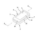
- FIG. 1 is a perspective view schematically illustrating an embodiment of a touch panel display device. Sectional drawing by the II-II line in FIG. FIG. 2 is a cross-sectional view showing a capacitive touch panel assembly of the display device of FIG. 1.
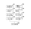
- FIG. 4 is a manufacturing process diagram showing a flow of manufacturing the capacitive touch panel assembly of FIG. 3;
- FIG. 7 is a simplified view for explaining a cover film material printing step in the manufacturing step of FIG. 4;
- the simplification figure for demonstrating a cover film extraction process.
- the simplification figure for explaining a cover film trimming process The figure which shows the film material for touch panels used for the manufacturing process of FIG. 4 simply.
- FIG. 7 is a simplified view for illustrating a state in which the second intermediate cover film is attached to the concave molding die and the second intermediate touch panel film is attached to the convex molding die in the insert molding step in the manufacturing process of FIG. 4;
- the manufacturing-process figure which shows the other example of the flow of manufacture of an electrostatic capacitance type touch panel assembly.
- FIG. 10 is a perspective view schematically showing another embodiment of the touch panel display device.
- FIG. 10 is a perspective view schematically showing another embodiment of the touch panel display device.
- the present invention is applied to a liquid crystal display device as a display device, but the present invention can be similarly applied to display devices of other forms such as an organic EL display device.
- the liquid crystal display device 2 shown in the figure includes a rectangular display device main body 3, and a display window 5 is provided on the surface (upper surface in FIG. 1) of the display device main body 3. It applies to the terminal etc.
- the liquid crystal display device 2 includes a rectangular device housing 4 having an open upper surface, the liquid crystal display means 6 is built in the device housing 4, and a capacitive touch panel assembly is provided on the surface side of the liquid crystal display means 6.
- a capacitive touch panel assembly 8 is mounted so as to cover the top opening of the device housing 4.
- the liquid crystal display means 6 may be known per se for displaying various information.
- the illustrated capacitive touch panel assembly 8 includes a capacitive touch panel 10, a resin layer 12, and an exterior cover 14.
- the capacitive touch panel 10 is configured of a touch panel film
- the first electrode pad 15M (FIGS. 9 to 10) is substantially entirely on one side (for example, the upper surface in FIGS. 2 and 3) of the touch panel film. 13) are provided in a matrix
- the first electrode pads 15M are positioned, for example, in the lateral direction (horizontal direction in FIGS. 9 to 12) based on the change in charge when the input operation is performed with a finger or the like of the hand.
- the second electrode pads 17M see FIG.
- the second electrode pads 17M are provided in a matrix form substantially over the other surface (the lower surface in FIG. 2), the second electrode pads 17M are subjected to an input operation using a finger or the like. Based on the change in charge, for example, the position in the vertical direction (vertical direction in FIGS. 9 to 13) is detected, and the electrostatic capacitance is detected based on the detected positions of the first and second electrode pads 15M and 17M. It is possible to detect the input operation position of the mold touch panel 10.
- the touch panel film of the capacitive touch panel 10 is formed of a transparent to translucent resin material, such as polyethylene terephthalate (PET), polycarbonate (PC), acrylic resin, etc., and the first and second electrode pads 15M and 17M are It is formed of a transparent conductive material such as indium tin oxide (ITO), polyethylenedioxyphene (PEDOT) as a conductive polymer which is an alternative to ITO, silver nanowire ink, silver halide particles and the like.
- a transparent to translucent resin material such as polyethylene terephthalate (PET), polycarbonate (PC), acrylic resin, etc.
- ITO indium tin oxide
- PEDOT polyethylenedioxyphene
- the capacitive touch panel 10 in which the first electrode pad 15M is provided on one side of the touch panel film and the second electrode pad 17M is provided on the other side is used.
- the first electrode pad may be provided in the first specific area on one side of the touch panel film, and the second electrode pad may be provided in another second specific area on this side, or one side of the touch panel film may be used.
- the first electrode pad may be provided, and the second electrode pad may be provided on the surface side of the first electrode pad via the electrically insulating layer.
- this capacitive touch panel 10 has a top wall 16 covering the surface side of the liquid crystal display means 6 and a circumferential side wall 18 extending from the outer peripheral portion of the top wall 16 to the liquid crystal display means 6 side.
- An extension 19 extends from a portion of the circumferential side wall 18 (the side wall 18a shown on the left side in FIG. 2).
- the first and second electrode pads 15M and 17M are provided on substantially the entire area of the top wall 16 of the capacitive touch panel 10, as will be understood from the description to be described later, and the circumferential side walls thereof.
- the first and second connection terminals (electrical connection portions) 15T and 17T electrically connected to the first and second electrode pads 15M and 17M are also provided in the extension portion 19 (see FIG. 10).
- the first and second connection terminals 15T and 17T are connected to a control substrate (not shown) of the liquid crystal display device 2. Therefore, it is possible to detect the position of a finger or the like who has performed an input operation and the movement of the finger by using the change in charge on the top wall 16 and the circumferential wall 18 of the capacitive touch panel 10.
- Such first and second electrode pads 15M and 17M do not need to be provided substantially over the entire area of the ceiling wall 16 and the circumferential side wall 18, and the top wall 16 corresponding to the input operation unit operated by a finger or the like. It may be provided on a part and part of the circumferential side wall 18, and even with this configuration, the desired effects described later can be achieved.
- the exterior cover 14 is formed of a cover film, has a rectangular shape corresponding to the shape of the device housing 4, and covers the top wall 20 covering the surface side of the top wall 16 of the capacitive touch panel 10. And a peripheral side wall 22 extending from the outer peripheral portion to the liquid crystal display means 6 side.
- the outer shape of the outer cover 14 is somewhat larger than the outer shape of the capacitive touch panel 10, and the resin layer 12 is interposed between the outer cover 14 (cover film) and the capacitive touch panel 10 (touch panel film). Ru.
- the resin layer 12 is formed by pouring a molten resin into the gap between the exterior cover 14 (cover film) and the capacitive touch panel 10 (touch panel film).
- the cover film of the exterior cover 14 is formed of a transparent to translucent resin material, such as polyethylene terephthalate (PET), polycarbonate (PC), acrylic resin, etc., similarly to the capacitive touch panel 10.
- a transparent to translucent resin material such as polyethylene terephthalate (PET), polycarbonate (PC), acrylic resin, etc.
- an opening area 24 (functioning as an input operation unit) is formed in a predetermined area of the inner surface of the exterior cover 14 (specifically, substantially the entire outer peripheral edge of the ceiling wall 20 and the entire peripheral wall 22).
- a printing layer 26 is provided. Accordingly, an open area 24 defined by the printing layer 26 is exposed from the outside of the exterior cover 14, and the open area 24 functions as the display window 5 of the liquid crystal display device 2. Thus, the capacitive touch panel 10 is operated to input.
- resin (resin of resin layer 12) used for insert molding transparent or translucent resin material, for example, acrylic resin, polycarbonate (PC), ABS resin etc. can be used.
- the exterior cover 14 (cover film) and the capacitive touch panel 10 (touch panel film) are manufactured prior to performing insert molding.
- printing is performed on one side of the transparent to translucent cover film material 32 to form the print layer 26 (cover film material printing step S ⁇ b> 1).
- cover film material 32 as described above, for example, a film of polyethylene terephthalate (PET) can be used.
- PET polyethylene terephthalate
- the cover film material printing step S1 as shown in FIG. 5, for example, printing of black, white, metallic tone, etc. is performed on a substantially rectangular annular predetermined area 34 which is somewhat larger than the top wall 20 of the exterior cover 14. And print in this manner to form a transparent to semitransparent rectangular opening area 24 at the center of the predetermined area 34, and this opening area 24 is a window of the exterior cover 14 (that is, the display of the liquid crystal display device 2). Act as a window 5).
- the print layer 26 of a predetermined area is formed at eight places at intervals in one film material 32 for a cover, but an appropriate number corresponding to the size of the film material 32 for a cover may be used. It can be made to print at one time.
- Such a printing layer 26 can be printed by an appropriate printing method such as screen printing or offset printing.
- cover film material 32 is punched to form the cover film piece 36 including the predetermined area 34 (cover film extraction step S2), and the thus-formed cover film becomes a cover film having the opening area 24. .
- this cover film removing step S2 for example, it can be performed by die cutting using a press die (not shown) or the like, and by die cutting as shown by a dashed dotted line 40 in FIG. A cover film piece 36 shown in FIG.
- cover film piece 36 shown in FIG. 6 is subjected to forming processing to form a first intermediate cover film 52 shown in FIG. 7 (cover film forming step S3).
- the cover film piece 36 is preheated to a predetermined temperature range, and the cover film piece 36 thus heated is set in a press die (not shown) and subjected to a forming process using a press die. That is, a convex forming die and a concave forming die are used as a press die, and a cover film piece 36 is interposed between both forming dies, and forming is performed by the convex forming die and the concave forming die, By this processing, the first intermediate cover film 52 having the shape shown in FIG. 7 is formed.
- This forming process can be processed by vacuum forming, pressure forming, or a combination thereof in addition to the above-described heat press forming.
- the first intermediate cover film 52 has a rising portion 54 extending upward (a portion corresponding to the circumferential side wall 22 of the exterior cover 14) and a flat portion 56 extending in a planar manner inward from the upper end portion of the rising portion 54.
- the predetermined area 34 provided with the print layer 26 includes the rising portion 54 and the annular flange 58 extending outward from the lower end portion of the rising portion 54). It extends to the outer peripheral edge of the flat portion 56 following the rising portion 54.
- trimming processing is performed on the first intermediate cover film 52 shown in FIG. 7 to remove unnecessary portions, and the second intermediate cover film 60 as shown in FIG. 8 is formed (cover film trimming step S4). Also in the cover film trimming step S4, similarly to the cover film removing step S2, for example, using a press die (not shown) or the like, the first intermediate cover film 52 is die-cut by this press die, and outward The second intermediate cover film 60 shown in FIG.
- the second intermediate cover film 60 is formed in substantially the same shape as the exterior cover 14 and has a rising portion 54 corresponding to the circumferential side wall 22 of the exterior cover 14 and a flat portion 56 corresponding to the top wall 20 thereof.
- the exterior cover 14 cover film
- the capacitive touch panel 10 can be manufactured in substantially the same manner as the exterior cover 14 as follows, for example.
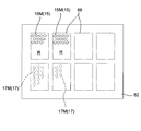
- the conductive pattern PT is formed on a transparent to semitransparent film material 62 for a touch panel.
- the conductive pattern PT includes the first and second conductive patterns 15 and 17.
- the first conductive pattern 15 is formed on one side of the touch panel film material 62.
- the second conductive pattern 17 is a touch panel film material 62.
- a film material 62 for a touch panel as described above, for example, a film of polyethylene terephthalate (PET) can be used.
- PET polyethylene terephthalate
- the first conductive pattern 15 is formed on a predetermined region R (a region surrounded by a dashed dotted line 66) of one side of the film material 62 ( Only a part of the first conductive pattern 15 is shown in FIGS. As shown in FIG. 10, the first conductive pattern 15 includes a plurality of first electrode pads 15M arranged in a matrix, a plurality of first connection terminals 15T, and a plurality of second connection terminals 17T.
- the predetermined region R has a region Ra and a region Rb (the boundary between the region Ra and the region Rb is shown by a dotted line 66a), and the first electrode pad 15M is formed substantially throughout the region Ra.
- the second connection terminals 15T and 17T are arranged in a line on one end side of the region Rb.
- the second conductive pattern 17 is formed on the other surface of the predetermined region R (note that, in FIGS. 9 and 10, a part of the second conductive pattern 17 is shown).
- the second conductive pattern 17 a large number of second electrode pads 17 M formed in a matrix over substantially the entire area on the other surface side of the region Ra and a third wiring 17 Lb connected to the second electrode pads are included. Inclusion, all of which are formed of transparent conductive materials as described above.
- through holes TH are formed in predetermined places of the film material 62 for a touch panel, and filling printing using a conductive material is performed on these through holes TH, thereby forming the second wiring 17Lb and the third wiring 17Lb corresponding to the second wiring 17Lb. Connect electrically. Further, carbon printing is performed on the first and second connection terminals 15T and 17T to apply carbon ink to the first and second connection terminals 15T and 17T. As described above, by applying the carbon ink to the first and second connection terminals 15T and 17T, the first and second connection terminals 15T and 17T are protected by the carbon ink, and the occurrence of the migration phenomenon is prevented.
- the sheet-like touch panel film material 62 is used, but a roll-like touch panel film material may be used.
- all the electrical connection portions are formed on one side of the film material 62 for touch panel, the electrical connection portions are formed on both sides of the film material 62 for touch panel.
- the second connection terminal 17T and the second wiring 17La are formed on the other surface of the touch panel film material 62, and the second wiring 17La and the third wiring 17Lb are formed in the through holes TH. It may be configured to be directly connected without interposing, and the formation of the through holes TH is not necessary.
- touch panel film material 62 is punched to form a touch panel film piece 64 (touch panel film removing step S6), and the touch panel film formed in this manner becomes a touch panel film.
- this touch panel film removing step S6 for example, it can be performed by a die cutting process using a press die (not shown) or the like, and as shown by an alternate long and short dash line 66 in FIG.
- the first conductive pattern 15 is present on one side of the touch panel film piece 64, and the second conductive pattern 17 is present on the other side.
- touch panel film piece 64 shown in FIG. 11 is subjected to forming processing to form a first intermediate touch panel film 68 shown in FIG. 12 (touch panel film forming step S7).
- touch panel film forming step S7 the touch panel film piece 64 is preheated to a predetermined temperature range, and the touch panel film piece 64 thus heated is set in a press mold (not shown) and subjected to forming processing by the press mold.
- a convex forming die and a concave forming die are used as a press die, and a touch panel film piece 64 is interposed between both forming dies, and forming is performed by the convex forming die and the concave forming die, By this processing, the first intermediate touch panel film 68 having the shape shown in FIG. 12 is formed.
- This forming process can be processed by vacuum forming, pressure forming, or a combination thereof in addition to the above-described heat press forming.
- the first intermediate touch panel film 68 has a rising portion 70 (portion corresponding to the circumferential side wall 18 of the capacitive touch panel 10) extending upward and a planar shape extending in a planar manner inward from the upper end portion of the rising portion 70.
- Portion 72 portion corresponding to the top wall 16 of the capacitive touch panel 10) and an annular flange 74 extending outward from the lower end portion of the rising portion 70, and the conductive pattern PT has a rising portion 70, a flat surface
- the first and second electrode pads 15 and 17M are present on the rising portion 70 and the flat portion 70, and the first and second connection terminals 15T are formed. , 17T are present on the annular flange 74.
- trimming processing is performed on the first intermediate touch panel film 68 shown in FIG. 12 to remove unnecessary portions, and the second intermediate touch panel film 76 as shown in FIG. 13 is formed (touch panel film trimming step S8).
- touch panel film trimming step S8 similarly to the touch panel film removing step S6, for example, using a press die (not shown) or the like, the first intermediate touch panel film 68 is die-cut by this press die, and outward
- the second intermediate touch panel film 76 shown in FIG. 13 is formed by removing a part (the part where the first and second connection terminals 15T and 17T are formed) leaving the annular flange 74 extending in the middle.
- the second intermediate touch panel film 76 is formed in substantially the same shape as the capacitive touch panel 10, and has a rising portion 70 corresponding to the circumferential side wall 18 of the capacitive touch panel 10 and a planar shape corresponding to the top wall 16 thereof. A portion 72 and a residual flange 78 corresponding to the extension 19 extending from the circumferential side wall 18 are formed, and thus, the capacitive touch panel 10 (touch panel film) is formed.
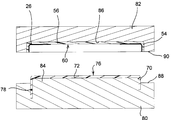
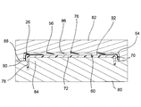
- the second intermediate cover film 60 (the outer cover 14) and the second intermediate touch panel film 76 (the capacitive touch panel 10) are insert-molded using a molding die (insert molding step S9).
- a second intermediate touch panel film is formed on the convex portion 84 of the convex molding die 80.
- the second intermediate cover film 60 is attached to the concave portion 86 of the concave molding die 82 while mounting 76, and in a state in which these are mounted, insert molding is performed to mold the above-described capacitive touch panel assembly 8.
- the convex molding die 80 is provided with a convex portion 84 corresponding to the inner surface side shape of the second intermediate touch panel film 76, and the second intermediate touch panel film 76 is mounted so as to cover the convex portion 84. Be done.
- the convex molding die 80 is provided with a groove portion into which the lower end portion of the rising portion 70 of the second intermediate touch panel film 76 and the residual flange 78 are inserted.
- the concave molding die 82 is provided with a concave portion 86 corresponding to the outer surface shape of the second intermediate cover film 60, and the second intermediate cover film 60 is mounted so as to be fitted into the concave portion 86. .
- the convex molding die 80 to which the second intermediate touch panel film 76 is attached and the concave molding die 82 to which the second intermediate cover film 60 is attached are clamped to form an injection port (not shown).
- Molten resin is injected into the cavity 92, and the molten resin injected into the cavity 92 is cooled and solidified to insert-mold the capacitive touch panel assembly 8 described above.
- the residual flange 78 on which the first and second connection terminals 15T and 17T are formed is inserted into the groove portion provided in the convex molding die 80, the residual flange 78 is formed.
- the molten resin does not go to the (first and second connection terminals 15T and 17T), and the flexible state is maintained.
- the capacitive touch panel assembly 8 manufactured in this manner is fixed to the surface side of the liquid crystal display means 6 by, for example, an OCA tape 94 as shown in FIG. 2, and thus the capacitive touch panel assembly
- the liquid crystal display device 2 provided with 8 is manufactured.
- this electrostatic capacitance type touch panel 8 can be configured as follows.
- the other surface of the outer cover 14 is used as a functional layer
- a hard coat layer may be provided, and in order to provide an antireflective function, an antireflective layer may be provided as a functional layer on the other surface of the exterior cover 14 and an antifouling function is provided.
- an antifouling layer as a functional layer may be provided on the other surface of the exterior cover 14, and a plurality of functional layers may be provided in layers to provide these plural functions.
- Such functional layers may be carried out before the cover film material printing step S1 or the cover film material printing step S1 and the cover film removing step S2 It can be simply and easily implemented by providing a functional layer at the stage of such a cover film.
- the print layer 26 is provided on one side of the exterior cover 14 to define the opening area 24.
- a vapor deposition layer by vapor deposition is provided instead of the print layer 26.
- 24 may be defined, or a design layer (design film) having a desired design pattern or the like may be formed instead of the print layer 26 or the like or together with the print layer 26 or the like.
- the flat portion 56 (corresponding to the top wall 20), the annular rising portion 54 (corresponding to the circumferential side wall 22) and the annular flange in the cover film forming step S3.
- the first intermediate cover film 52 having the 58 is formed, it is not limited to such a configuration, and it is not necessary to form the annular rising portion 54 and the annular flange 58 in an annular shape, and some of them are cut. It can also be formed as an integral part.
- the capacitive touch panel 10 also has a flat portion 72 (corresponding to the top wall 16), an annular rising portion 70 (corresponding to the circumferential side wall 18) and an annular flange 74 in the touch panel film forming step S7.
- the intermediate touch panel film 68 is formed, it is not limited to such a configuration, and it is not necessary to form the annular rising portion 70 and the annular flange 74 in an annular shape, and some of them may be cut away. It can also be formed into
- the second intermediate cover film 60 subjected to the trimming processing for the exterior cover 14 is trimmed for the capacitive touch panel 10.
- the insert molding is performed using the second intermediate touch panel film 76 subjected to the above-described method.
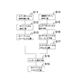
- it can be manufactured according to the manufacturing process shown in FIG.
- the first intermediate cover film 52 is manufactured by performing the cover film material printing step S 11, the cover film removing step S 12 and the cover film forming step S 13, and the capacitive touch panel 10.
- a second intermediate touch panel film 76 is manufactured by performing the conductive pattern forming step S14, the touch panel film removing step S15, the touch panel film forming step S15, and the touch panel film trimming step S17.
- the first intermediate cover film 52 after the cover film forming step S13 and the second intermediate touch panel film 76 after the touch panel film trimming step S17 are insert-molded to produce an intermediate touch panel assembly (insert molding step S18), and then the intermediate touch panel The first intermediate cover film of the assembly is trimmed to remove unnecessary portions of the first intermediate cover film 52 (cover film trimming step S19), and the capacitive touch panel assembly 10 can be manufactured in this manner as well. .
- the second intermediate cover film 60 is manufactured by performing the film material printing process for the cover, the cover film removing process, the cover film forming process, and the cover film trimming process.
- the first intermediate touch panel film 68 is manufactured by performing the conductive pattern forming process, the touch panel film removing process, and the touch panel film forming process.
- the second intermediate cover film 60 after the cover film trimming process and the first intermediate touch panel film 68 after the touch panel film forming process are insert-molded to produce an intermediate touch panel assembly (insert molding process).
- a trimming process is performed on the intermediate touch panel film to remove an unnecessary portion of the first intermediate touch panel film 68 (touch panel film trimming step), and the capacitive touch panel assembly 10 can be manufactured also in this manner.
- the manufacturing process related to the exterior cover 14 (cover film) and the capacitive touch panel 10 (touch panel film) can be improved. That is, for the exterior cover 14 (cover film), the first intermediate cover film 52 is manufactured by performing the film material printing process for the cover, the cover film removing process and the cover film forming process, and the capacitive touch panel 10 ( As for the touch panel film, the first intermediate touch panel film 68 is manufactured by performing the conductive pattern forming step, the touch panel film removing step and the touch panel film forming step. Then, the first intermediate cover film 52 after the cover film forming process and the first intermediate touch panel film 68 after the touch panel film forming process are insert-molded to produce an intermediate touch panel assembly (insert molding process).
- the cover film 52 and the first intermediate touch panel film 68 are subjected to trimming processing to simultaneously remove unnecessary portions of the first intermediate cover film 52 and the first intermediate touch panel film 68 (cover film trimming step and touch panel film trimming step)
- the capacitive touch panel assembly 10 can be manufactured.
- the opening area 24 of the exterior cover 14 functions as an input operation unit (input operation screen), but the top wall 16 and the periphery of the capacitive pattern film 10 in this embodiment Since the side walls 18 are provided with the first and second electrode pads 15M and 17M in the form of a matrix, at least a part of the top wall 16 and the peripheral side surface of the capacitive touch panel 10 is used.
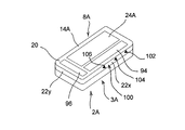
- at least a partial area of the circumferential side wall 22 can function as an input operation unit, and can be configured, for example, as shown in FIG.
- the first sub opening region 94 is on the right side in FIG.
- the second sub opening region 96 is provided on the lower side in FIG.
- the main opening area 24A functions as a display window and an input operation unit equivalent to the opening area 24 in the embodiment described above.
- the first sub opening area 94 is an input operation area 102 (input operation unit) provided on the side wall 22x of the exterior cover 14A (the side wall adjacent to the first sub opening area 94 and the side wall of the display device main body 3A).
- Function is provided to display the operation content of the input operation area 102, and the input operation is performed on the portion of the side wall 22x corresponding to the operation information displayed in the first sub opening area 94.
- the input operation can be detected by the change in charge on the side wall (not shown) of the capacitive touch panel (the side wall located inside the side wall 22x of the exterior cover 14A).
- notations such as symbols and figures indicating the contents of the operation may be added.
- the symbol 102 is used as an input unit such as "volume loud”, “zoom expansion”, “forward”, etc.
- the symbol 104 can be used as an input unit such as “volume reduction”, “zoom reduction”, “backward” and the like, and the symbol 106 can be used as an input unit such as “on / off of sound”.
- An LED or the like can be easily incorporated inside the operation unit, and the operation state can be visually recognized by turning on / off the operation unit.
- the first sub opening area 94 may be provided on the side wall 22 x of the exterior cover 14 A.
- the first sub opening area 94 functions as a display window and an input operation unit.
- the operation information displayed on the screen is directly input and operated from the first sub opening area 94.
- the second sub opening area 94 corresponds to an input operation area (not shown) (functioning as an input operation unit) provided on the side wall 22 y of the exterior cover 14 A (side wall adjacent to the second sub opening area 96). , And is for displaying the operation content of the input operation area, and the input operation is performed by inputting the portion of the side wall 22y corresponding to the operation information displayed in the second sub opening area 96.
- the input operation can be detected by the change in charge on the side wall (not shown) of the capacitive touch panel (the side wall located inside the side wall 22y of the exterior cover 14A).
- the second sub opening area 96 may also be provided on the side wall 22y of the exterior cover 14A.
- the second sub opening area 96 functions as a display window and an input operation unit.
- the operation information displayed in the opening area 96 is directly input and operated from the second sub opening area 96.
- the liquid crystal display device 2A since the first and second sub opening regions 94 and 96 are provided in addition to the main opening region 24A, the liquid crystal display device 2A can have more functions. The operability at the time of operating those functions can be improved, and the liquid crystal display device 2A more convenient can be provided. In addition, one or three or more sub-opening regions may be provided, and the arrangement can also be provided at an appropriate site in consideration of usage and the like.
- Such a liquid crystal display device 2A can be applied to a smartphone, a tablet terminal, a digital camera, etc., and when the touch panel operation function is provided on the side, input operation such as volume, zoom, channel switching, power ON / OFF, etc. Can be set on the side surface of the display device main body 3A without individually setting the operation button or the like.
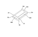
- the main opening area 24A, the first sub opening area 94, and the second sub opening area 96 are flat surfaces of the exterior cover 14A of the capacitive touch panel assembly 8A (ie, Although provided on the top wall 20 and the side walls 22x and 22y), the opening region can also be provided on a curved surface, and can be configured, for example, as shown in FIG.
- the connecting portion between the top wall 20 and the side wall 22x of the exterior cover 14B has a relatively large R shape, and the first sub opening region 94B is provided along the R shape. .
- the connecting portion between the top wall 20 and the side wall 22y has a relatively large R shape, and the second sub opening region 96B is provided along the R shape.
- the first and second sub opening regions 94B and 96B function as a display window and an input operation unit (touch panel input operation unit), and the operation information displayed in the first and second sub opening regions 94B and 96B is Direct operation is performed from the first and second sub opening regions 94B and 96B.
- the first and second sub aperture regions 94B and 96B are provided, so that the liquid crystal display device 2B can have many functions. The operability at the time of operating those functions can be improved, and a more convenient liquid crystal display device 2B can be provided. Also in this case, one or three or more sub opening regions may be provided. When the sub opening region is provided at the connecting portion between the top wall 20 and the circumferential side wall 22 as described above, the shape of the liquid crystal display means 6 may be made to correspond to the R shape of the connecting portion.
- the surface (upper surface) is formed in a flat shape, but it may be a curved surface, and / or the top wall 20 and the circumferential side wall 22.
- the connection portion with the above can also be made a relatively large R shape, regardless of the presence or absence of the sub opening region.
- the shape of the liquid crystal display device is not limited to this, and may be, for example, another shape such as a circle, an ellipse, or a polygon. It can also be done.
- Such a capacitive touch panel assembly can also be manufactured, for example, as follows, using the capacitive touch panel (after the touch panel film trimming process) manufactured as described above. .
- the exterior cover 14 (second intermediate cover film 60) and the capacitive touch panel 10 (second intermediate touch panel film 76) are simultaneously insert-molded in one step, as follows. Can also be made in one step.
- the capacitive touch panel 10 (second intermediate touch panel film 76) is attached to the convex portion of the first convex molding die, and A film having a design pattern or the like is provided on the concave portion side of the concave molding die, and in such a state, the first convex molding die and the first concave molding die are clamped to insert the capacitive touch panel 10 as an insert.
- in-mold molding in which a design pattern of a film or the like is applied to the surface of the resin layer formed by molding at the same time as this insert molding is carried out.
- the capacitive touch panel assembly can be manufactured.
- an exterior cover can be abbreviate
- the exterior cover is omitted, but the capacitive touch panel 10 (second intermediate touch panel film 76) is molded in-mold as described above and the resin layer 12 is formed on the surface thereof.
- the outer cover is formed by the above-described in-mold molding, and in-mold formed on the resin layer 12 on the surface side of the capacitive touch panel 10 via OCA (Optical Clear Adhesive) (for example, OCA tape)
- OCA Optical Clear Adhesive
- the exterior cover may be attached.
- the capacitive touch panel assembly may be manufactured by insert molding and pasting.
- the exterior cover 14 (second intermediate cover film 60) manufactured as described above (or another manufacturing method in advance) It can manufacture using the exterior cover and the electrostatic capacitance type touch panel 10 (2nd intermediate
- the capacitive touch panel 10 (second intermediate touch panel film 76) is mounted on the convex portion of the convex molding die, and the convex molding gold is thus mounted
- the mold and the concave mold are clamped, and the capacitive touch panel 10 is insert-molded to form the resin layer 12 on the surface side.
- the exterior cover 14 (second intermediate cover film 60) is attached by OCA to the surface side (surface side of the insert-molded resin layer 12) of the capacitive touch panel 10 (second intermediate touch panel film 76). Even in such a case, the capacitive touch panel assembly including the capacitive touch panel 10 can be manufactured.
- the exterior cover 14 is provided in the embodiment described above, the exterior cover 14 is not necessarily required, and the resin layer 12 can also function as the exterior cover.
- the capacitive touch panel 10 (second intermediate touch panel film 76) is mounted on the convex portion of the convex molding die, and the convex is formed in the mounted state.
- Mold mold and concave mold are clamped, and the capacitive touch panel 10 is insert molded to form the resin layer 12 on the surface side, and printing, painting on the surface side of the insert molded resin layer 12,
- a design pattern or the like may be added by secondary processing such as vapor deposition, or a functional layer (anti-scratching function, anti-reflection function, anti-staining function, etc.) may be added.
- a capacitive touch panel assembly including the capacitive touch panel 10 can be manufactured.
- the resin layer 12 is formed by insert molding on the surface side of the capacitive touch panel 10 (second intermediate touch panel film 76), but as the resin layer 12 instead of insert molding.
- a functional resin three-dimensional plate (or a resin three-dimensional sheet) may be attached to the capacitive touch panel 10 (second intermediate touch panel film 76).
- a three-dimensional resin plate (or three-dimensional resin sheet) is formed in advance three-dimensionally by molding so as to correspond to the outer shape of the capacitive touch panel 10, and formed.
- a design pattern or the like is added to, for example, the back side (or the front side) of the three-dimensional sheet), and a functional layer (such as a scratch prevention mechanism) is further added to the front side.
- a resin-made three-dimensional plate (or a resin-made three-dimensional sheet) may be attached by OCA on the surface side of the intermediate touch panel film 76), and even in this case, the static type provided with the capacitive touch panel 10 Capacitive touch panel assemblies can be manufactured.
- a resin-made three-dimensional plate (or a resin-made three-dimensional sheet) that functions as the resin layer 12 is formed in advance as described above, and this resin-made three-dimensional plate ( Alternatively, the capacitive touch panel 10 (second intermediate touch panel film 76) and the exterior cover 14 (second intermediate cover film 60) may be attached to a resin-made three-dimensional sheet.
- a resin-made three-dimensional plate (or resin-made three-dimensional sheet) is attached to the surface side of the capacitive touch panel 10 (second intermediate touch panel film 76) with OCA, and this resin-made three-dimensional plate (or The exterior cover 14 (second intermediate cover film 60) may be attached to the surface side of the resin three-dimensional sheet via the OCA, and even in this way, the capacitive touch panel assembly including the capacitive touch panel 10 Can be manufactured.
Landscapes
- Engineering & Computer Science (AREA)
- General Engineering & Computer Science (AREA)
- Theoretical Computer Science (AREA)
- Human Computer Interaction (AREA)
- Physics & Mathematics (AREA)
- General Physics & Mathematics (AREA)
- Position Input By Displaying (AREA)
Abstract
La présente invention concerne un procédé de fabrication pour l'assemblage d'un panneau tactile de type capacitif qui permet de fabriquer facilement un film de panneau tactile d'une forme prédéterminée à partir de matériaux de film pour un panneau de type capacitif. La présente invention comprend les étapes suivantes : une étape de formage d'un film de panneau tactile (S7) servant à former un premier film de panneau tactile intermédiaire par application d'un processus de formage à un matériau de film pour un panneau tactile dans lequel un premier motif conducteur et un deuxième motif conducteur sont formés sur un film transparent ou semi-transparent ; et une étape de découpe du film du panneau tactile (S8) servant à appliquer un processus de découpe au premier film de panneau tactile intermédiaire après l'étape de formage du panneau tactile (S7). Au cours de l'étape de formage du panneau tactile (S8), un deuxième film de panneau tactile intermédiaire est formé par application d'un processus de découpe au premier film de panneau tactile intermédiaire.
Priority Applications (1)
| Application Number | Priority Date | Filing Date | Title |
|---|---|---|---|
| JP2013526885A JP5997158B2 (ja) | 2011-07-29 | 2012-07-27 | 静電容量型タッチパネルアセンブリ及びこれを備えた表示装置 |
Applications Claiming Priority (2)
| Application Number | Priority Date | Filing Date | Title |
|---|---|---|---|
| JP2011-166413 | 2011-07-29 | ||
| JP2011166413 | 2011-07-29 |
Publications (1)
| Publication Number | Publication Date |
|---|---|
| WO2013018698A1 true WO2013018698A1 (fr) | 2013-02-07 |
Family
ID=47629222
Family Applications (1)
| Application Number | Title | Priority Date | Filing Date |
|---|---|---|---|
| PCT/JP2012/069145 Ceased WO2013018698A1 (fr) | 2011-07-29 | 2012-07-27 | Procédé de fabrication pour l'assemblage d'un panneau tactile de type capacitif et dispositif d'affichage équipé de celui-ci |
Country Status (2)
| Country | Link |
|---|---|
| JP (1) | JP5997158B2 (fr) |
| WO (1) | WO2013018698A1 (fr) |
Cited By (8)
| Publication number | Priority date | Publication date | Assignee | Title |
|---|---|---|---|---|
| CN104331209A (zh) * | 2014-11-27 | 2015-02-04 | 中环高科(天津)股份有限公司 | 一种采用导电高分子材料制作一体化触控电容屏的方法 |
| CN104331207A (zh) * | 2014-11-27 | 2015-02-04 | 中环高科(天津)股份有限公司 | 一种采用石墨烯材料制作一体化触控电容屏的方法 |
| TWI494809B (zh) * | 2013-05-09 | 2015-08-01 | Au Optronics Corp | 觸控面板 |
| JP2016118622A (ja) * | 2014-12-19 | 2016-06-30 | エルジー ディスプレイ カンパニー リミテッド | 液晶モジュール及び液晶表示装置 |
| JP2016194746A (ja) * | 2015-03-31 | 2016-11-17 | 大日本印刷株式会社 | タッチパネルセンサ用中間部材、及び、タッチパネルセンサの製造方法 |
| WO2019142748A1 (fr) * | 2018-01-16 | 2019-07-25 | 積水ポリマテック株式会社 | Capteur de capacité |
| JP2019164828A (ja) * | 2013-11-15 | 2019-09-26 | 株式会社半導体エネルギー研究所 | 情報処理装置 |
| JP2019194891A (ja) * | 2019-06-21 | 2019-11-07 | カシオ計算機株式会社 | 入力装置及び電子機器 |
Citations (6)
| Publication number | Priority date | Publication date | Assignee | Title |
|---|---|---|---|---|
| JPS62154413A (ja) * | 1985-12-26 | 1987-07-09 | 三菱レイヨン株式会社 | 凹凸面を有する透明電極化樹脂の製造方法 |
| JP2001162619A (ja) * | 1999-12-09 | 2001-06-19 | Nissha Printing Co Ltd | インサート成形用シートとこれを用いたインサート成形品 |
| JP2009130283A (ja) * | 2007-11-27 | 2009-06-11 | Alps Electric Co Ltd | 電子機器用外観ケースおよびその製造方法 |
| JP2010086530A (ja) * | 2008-10-02 | 2010-04-15 | Samsung Electronics Co Ltd | 電子機器ケース及びその製造方法 |
| WO2010058829A1 (fr) * | 2008-11-21 | 2010-05-27 | 株式会社 翔栄 | Structure de support d'écran tactile et procédé de fabrication de celle-ci |
| JP2010214601A (ja) * | 2009-03-13 | 2010-09-30 | Shimada Precision Kk | フィルムインサート成形品及びその製造方法並びにこれを備えた液晶表示装置 |
Family Cites Families (1)
| Publication number | Priority date | Publication date | Assignee | Title |
|---|---|---|---|---|
| US20090314550A1 (en) * | 2008-06-18 | 2009-12-24 | Layton Michael D | Touchpad designed in a planar configuration that can be molded to conform to a non-planar object |
-
2012
- 2012-07-27 JP JP2013526885A patent/JP5997158B2/ja active Active
- 2012-07-27 WO PCT/JP2012/069145 patent/WO2013018698A1/fr not_active Ceased
Patent Citations (6)
| Publication number | Priority date | Publication date | Assignee | Title |
|---|---|---|---|---|
| JPS62154413A (ja) * | 1985-12-26 | 1987-07-09 | 三菱レイヨン株式会社 | 凹凸面を有する透明電極化樹脂の製造方法 |
| JP2001162619A (ja) * | 1999-12-09 | 2001-06-19 | Nissha Printing Co Ltd | インサート成形用シートとこれを用いたインサート成形品 |
| JP2009130283A (ja) * | 2007-11-27 | 2009-06-11 | Alps Electric Co Ltd | 電子機器用外観ケースおよびその製造方法 |
| JP2010086530A (ja) * | 2008-10-02 | 2010-04-15 | Samsung Electronics Co Ltd | 電子機器ケース及びその製造方法 |
| WO2010058829A1 (fr) * | 2008-11-21 | 2010-05-27 | 株式会社 翔栄 | Structure de support d'écran tactile et procédé de fabrication de celle-ci |
| JP2010214601A (ja) * | 2009-03-13 | 2010-09-30 | Shimada Precision Kk | フィルムインサート成形品及びその製造方法並びにこれを備えた液晶表示装置 |
Cited By (14)
| Publication number | Priority date | Publication date | Assignee | Title |
|---|---|---|---|---|
| TWI494809B (zh) * | 2013-05-09 | 2015-08-01 | Au Optronics Corp | 觸控面板 |
| US10755667B2 (en) | 2013-11-15 | 2020-08-25 | Semiconductor Energy Laboratory Co., Ltd. | Data processor |
| JP2019164828A (ja) * | 2013-11-15 | 2019-09-26 | 株式会社半導体エネルギー研究所 | 情報処理装置 |
| JP2022002125A (ja) * | 2013-11-15 | 2022-01-06 | 株式会社半導体エネルギー研究所 | 情報処理装置 |
| US11244648B2 (en) | 2013-11-15 | 2022-02-08 | Semiconductor Energy Laboratory Co., Ltd. | Data processor |
| US11626083B2 (en) | 2013-11-15 | 2023-04-11 | Semiconductor Energy Laboratory Co., Ltd. | Data processor |
| US12142239B2 (en) | 2013-11-15 | 2024-11-12 | Semiconductor Energy Laboratory Co., Ltd. | Data processor |
| CN104331207A (zh) * | 2014-11-27 | 2015-02-04 | 中环高科(天津)股份有限公司 | 一种采用石墨烯材料制作一体化触控电容屏的方法 |
| CN104331209A (zh) * | 2014-11-27 | 2015-02-04 | 中环高科(天津)股份有限公司 | 一种采用导电高分子材料制作一体化触控电容屏的方法 |
| JP2016118622A (ja) * | 2014-12-19 | 2016-06-30 | エルジー ディスプレイ カンパニー リミテッド | 液晶モジュール及び液晶表示装置 |
| JP2016194746A (ja) * | 2015-03-31 | 2016-11-17 | 大日本印刷株式会社 | タッチパネルセンサ用中間部材、及び、タッチパネルセンサの製造方法 |
| WO2019142748A1 (fr) * | 2018-01-16 | 2019-07-25 | 積水ポリマテック株式会社 | Capteur de capacité |
| JPWO2019142748A1 (ja) * | 2018-01-16 | 2020-01-23 | 積水ポリマテック株式会社 | 静電容量センサ |
| JP2019194891A (ja) * | 2019-06-21 | 2019-11-07 | カシオ計算機株式会社 | 入力装置及び電子機器 |
Also Published As
| Publication number | Publication date |
|---|---|
| JP5997158B2 (ja) | 2016-09-28 |
| JPWO2013018698A1 (ja) | 2015-03-05 |
Similar Documents
| Publication | Publication Date | Title |
|---|---|---|
| JP5997158B2 (ja) | 静電容量型タッチパネルアセンブリ及びこれを備えた表示装置 | |
| US9335871B2 (en) | Surface panel and method of manufacturing the same | |
| JP6941732B2 (ja) | マルチパートデバイスエンクロージャ | |
| JP5066182B2 (ja) | インサート成形用積層物とその製造方法、インサート成形品とその製造方法 | |
| US9280241B2 (en) | Touch panel and method for manufacturing | |
| CN203982334U (zh) | 具有指纹识别功能的触控面板 | |
| JP6047279B2 (ja) | 静電容量センサー及びその製造方法 | |
| JP5225178B2 (ja) | 静電容量センサ及びその製造方法 | |
| JPWO2005081210A1 (ja) | 電子機器表示窓の保護パネル及び保護パネルの製造方法 | |
| TW201601026A (zh) | 具有指紋識別功能的觸控面板 | |
| JP2013114673A (ja) | タッチモジュールの製造方法 | |
| CN102124428A (zh) | 表面平坦性优良且带有触摸输入功能的保护面板及具有该保护面板的电子器件 | |
| CN108139832B (zh) | 输入装置以及输入装置的制造方法 | |
| JP2012043165A (ja) | 成形部材及び透光型入力装置 | |
| KR20110000762A (ko) | 터치 입력 기능을 구비한 보호 패널 | |
| CN103853366A (zh) | 应用在触控面板的粘合层及其制备方法 | |
| US20140055958A1 (en) | 3d touch module and its methode of manufacturing | |
| WO2013100161A1 (fr) | Unité d'écran tactile | |
| JP3167028U (ja) | タッチパネルの装飾枠 | |
| JP2015209349A (ja) | フィルム一体ガラス、フィルム材、及びフィルム材の製造方法 | |
| JP2013221985A (ja) | ディスプレイ用カバー部材およびその製造方法 | |
| JP5917354B2 (ja) | 検知機能を有する表面パネル | |
| JP2016173736A (ja) | センサーパネル及びセンサーパネルの製造方法 | |
| KR20140051055A (ko) | 검지 기능을 갖는 표면 패널 및 그 제조 방법 | |
| JP2012098973A (ja) | ガラス複合体及びそのガラス複合体を用いた入力装置 |
Legal Events
| Date | Code | Title | Description |
|---|---|---|---|
| 121 | Ep: the epo has been informed by wipo that ep was designated in this application |
Ref document number: 12819491 Country of ref document: EP Kind code of ref document: A1 |
|
| ENP | Entry into the national phase |
Ref document number: 2013526885 Country of ref document: JP Kind code of ref document: A |
|
| NENP | Non-entry into the national phase |
Ref country code: DE |
|
| 122 | Ep: pct application non-entry in european phase |
Ref document number: 12819491 Country of ref document: EP Kind code of ref document: A1 |