WO2013076830A1 - 電子部品およびその製造方法 - Google Patents
電子部品およびその製造方法 Download PDFInfo
- Publication number
- WO2013076830A1 WO2013076830A1 PCT/JP2011/076962 JP2011076962W WO2013076830A1 WO 2013076830 A1 WO2013076830 A1 WO 2013076830A1 JP 2011076962 W JP2011076962 W JP 2011076962W WO 2013076830 A1 WO2013076830 A1 WO 2013076830A1
- Authority
- WO
- WIPO (PCT)
- Prior art keywords
- side wall
- substrate
- outer periphery
- electronic component
- wafer
- Prior art date
- Legal status (The legal status is an assumption and is not a legal conclusion. Google has not performed a legal analysis and makes no representation as to the accuracy of the status listed.)
- Ceased
Links
Images


Classifications
-
- H—ELECTRICITY
- H03—ELECTRONIC CIRCUITRY
- H03H—IMPEDANCE NETWORKS, e.g. RESONANT CIRCUITS; RESONATORS
- H03H9/00—Networks comprising electromechanical or electro-acoustic elements; Electromechanical resonators
- H03H9/02—Details
- H03H9/05—Holders or supports
- H03H9/10—Mounting in enclosures
- H03H9/1057—Mounting in enclosures for microelectro-mechanical devices
-
- H—ELECTRICITY
- H10—SEMICONDUCTOR DEVICES; ELECTRIC SOLID-STATE DEVICES NOT OTHERWISE PROVIDED FOR
- H10W—GENERIC PACKAGES, INTERCONNECTIONS, CONNECTORS OR OTHER CONSTRUCTIONAL DETAILS OF DEVICES COVERED BY CLASS H10
- H10W76/00—Containers; Fillings or auxiliary members therefor; Seals
- H10W76/10—Containers or parts thereof
- H10W76/12—Containers or parts thereof characterised by their shape
-
- B—PERFORMING OPERATIONS; TRANSPORTING
- B23—MACHINE TOOLS; METAL-WORKING NOT OTHERWISE PROVIDED FOR
- B23K—SOLDERING OR UNSOLDERING; WELDING; CLADDING OR PLATING BY SOLDERING OR WELDING; CUTTING BY APPLYING HEAT LOCALLY, e.g. FLAME CUTTING; WORKING BY LASER BEAM
- B23K1/00—Soldering, e.g. brazing, or unsoldering
- B23K1/0008—Soldering, e.g. brazing, or unsoldering specially adapted for particular articles or work
- B23K1/0016—Soldering of electronic components
-
- B—PERFORMING OPERATIONS; TRANSPORTING
- B81—MICROSTRUCTURAL TECHNOLOGY
- B81B—MICROSTRUCTURAL DEVICES OR SYSTEMS, e.g. MICROMECHANICAL DEVICES
- B81B7/00—Microstructural systems ; Auxiliary parts of microstructural devices or systems
- B81B7/0032—Packages or encapsulation
- B81B7/0035—Packages or encapsulation for maintaining a controlled atmosphere inside of the chamber containing the MEMS
- B81B7/0041—Packages or encapsulation for maintaining a controlled atmosphere inside of the chamber containing the MEMS maintaining a controlled atmosphere with techniques not provided for in B81B7/0038
-
- B—PERFORMING OPERATIONS; TRANSPORTING
- B81—MICROSTRUCTURAL TECHNOLOGY
- B81C—PROCESSES OR APPARATUS SPECIALLY ADAPTED FOR THE MANUFACTURE OR TREATMENT OF MICROSTRUCTURAL DEVICES OR SYSTEMS
- B81C1/00—Manufacture or treatment of devices or systems in or on a substrate
- B81C1/00865—Multistep processes for the separation of wafers into individual elements
- B81C1/00873—Multistep processes for the separation of wafers into individual elements characterised by special arrangements of the devices, allowing an easier separation
-
- H—ELECTRICITY
- H10—SEMICONDUCTOR DEVICES; ELECTRIC SOLID-STATE DEVICES NOT OTHERWISE PROVIDED FOR
- H10W—GENERIC PACKAGES, INTERCONNECTIONS, CONNECTORS OR OTHER CONSTRUCTIONAL DETAILS OF DEVICES COVERED BY CLASS H10
- H10W72/00—Interconnections or connectors in packages
- H10W72/01—Manufacture or treatment
- H10W72/0198—Manufacture or treatment batch processes
-
- B—PERFORMING OPERATIONS; TRANSPORTING
- B23—MACHINE TOOLS; METAL-WORKING NOT OTHERWISE PROVIDED FOR
- B23K—SOLDERING OR UNSOLDERING; WELDING; CLADDING OR PLATING BY SOLDERING OR WELDING; CUTTING BY APPLYING HEAT LOCALLY, e.g. FLAME CUTTING; WORKING BY LASER BEAM
- B23K2101/00—Articles made by soldering, welding or cutting
- B23K2101/36—Electric or electronic devices
- B23K2101/42—Printed circuits
-
- B—PERFORMING OPERATIONS; TRANSPORTING
- B81—MICROSTRUCTURAL TECHNOLOGY
- B81B—MICROSTRUCTURAL DEVICES OR SYSTEMS, e.g. MICROMECHANICAL DEVICES
- B81B2201/00—Specific applications of microelectromechanical systems
- B81B2201/01—Switches
- B81B2201/012—Switches characterised by the shape
- B81B2201/014—Switches characterised by the shape having a cantilever fixed on one side connected to one or more dimples
-
- H—ELECTRICITY
- H03—ELECTRONIC CIRCUITRY
- H03H—IMPEDANCE NETWORKS, e.g. RESONANT CIRCUITS; RESONATORS
- H03H3/00—Apparatus or processes specially adapted for the manufacture of impedance networks, resonating circuits, resonators
- H03H3/007—Apparatus or processes specially adapted for the manufacture of impedance networks, resonating circuits, resonators for the manufacture of electromechanical resonators or networks
- H03H3/0072—Apparatus or processes specially adapted for the manufacture of impedance networks, resonating circuits, resonators for the manufacture of electromechanical resonators or networks of microelectro-mechanical resonators or networks
-
- H—ELECTRICITY
- H10—SEMICONDUCTOR DEVICES; ELECTRIC SOLID-STATE DEVICES NOT OTHERWISE PROVIDED FOR
- H10W—GENERIC PACKAGES, INTERCONNECTIONS, CONNECTORS OR OTHER CONSTRUCTIONAL DETAILS OF DEVICES COVERED BY CLASS H10
- H10W76/00—Containers; Fillings or auxiliary members therefor; Seals
- H10W76/60—Seals
-
- H—ELECTRICITY
- H10—SEMICONDUCTOR DEVICES; ELECTRIC SOLID-STATE DEVICES NOT OTHERWISE PROVIDED FOR
- H10W—GENERIC PACKAGES, INTERCONNECTIONS, CONNECTORS OR OTHER CONSTRUCTIONAL DETAILS OF DEVICES COVERED BY CLASS H10
- H10W95/00—Packaging processes not covered by the other groups of this subclass
Definitions
- the embodiment described below relates to an electronic component and a manufacturing method thereof.
- Wafer level packaging technology is a technology that encapsulates a large number of elements formed on a semiconductor wafer in a lump before dividing the semiconductor wafer into individual chips. Since it can be formed in the size of individual chips, it is widely used in the manufacture of small semiconductor devices.
- an electronic component has a movable part
- a lid member covering the element is placed on the wafer, and the lid member is placed on the wafer. It is desirable to seal so as to define a space surrounding the element.
- Patent Document 1 discloses a method in which an element is formed in a recess on the wafer surface, and a lid member is bonded to the surface of the wafer via a brazing material to seal the element. Further, in Patent Document 2, a lid member is bonded to the upper surface of an outer peripheral wall member formed on the wafer so as to surround the element via a brazing material layer, thereby sealing the element.
- the brazing material layer when joining the lid member to the wafer surface or the upper surface of the outer peripheral wall member formed on the wafer surface via the brazing material layer, it is necessary to melt the brazing material layer, and the molten brazing material It is preferable to lightly press the lid member so that the layer can absorb the irregularities on the substrate surface and the lid member surface to obtain reliable sealing.
- the molten brazing material layer when the molten brazing material layer is pressed, the brazing material may flow out or be pushed out into the space surrounding the element.
- the brazing material that has flowed out contacts the element it not only causes an electrical failure, but particularly in the case of an element having a movable part, the operation of the movable part is hindered.
- an electronic component is disposed on a substrate, an element formed on the substrate, a side wall member surrounding the element on the substrate, and the side wall member.
- a lid member that defines a space surrounding the element on the substrate; and a sealing member that is provided outside the side wall member, joins the side wall member and the lid member to the surface of the substrate, and seals the space.
- an electronic component manufacturing method includes a step of forming a plurality of elements on a wafer in a matrix, and a plurality of lid members respectively corresponding to the plurality of elements are formed in a matrix.
- the member includes a side wall surrounding the corresponding element, the adjacent lid members are separated from each other by a groove portion, and the adjacent lid members are connected to each other by a bridging portion that bridges the groove portion.
- a method of manufacturing an electronic component includes a step of forming a plurality of elements in a matrix on a wafer, and the surface of the wafer is erected so as to surround the plurality of elements on the wafer.
- a step of forming a plurality of side wall members as a seal ring, a plurality of lid members respectively corresponding to the plurality of elements are formed in a matrix, adjacent lid members are separated from each other by a groove portion, and adjacent lid members
- An element of the sealing member is formed by enclosing the element on the substrate with the lid member and the side wall member, and sealing the element by coupling the side wall member and the lid member to the substrate surface by the sealing member outside the side wall member. It is possible to avoid the protrusion to the existing space.
- FIG. 3 is a process cross-sectional view (part 1) illustrating a process of forming a main body portion of the MEMS switch of FIG.
- FIG. 3 is a process cross-sectional view (part 2) illustrating a process of forming a main body portion of the MEMS switch of FIG.
- FIG. 6 is a process cross-sectional view (part 3) illustrating the process of forming the main body of the MEMS switch of FIG. 1;
- FIG. 6 is a process cross-sectional view (part 4) illustrating a process of forming a main body portion of the MEMS switch in FIG. 1;
- FIG. 6 is a process cross-sectional view (part 5) illustrating a process of forming a main body portion of the MEMS switch of FIG. 1;
- FIG. 6 is a process cross-sectional view (part 6) illustrating a process of forming a main body portion of the MEMS switch in FIG. 1;
- FIG. 8 is a process cross-sectional view (part 7) illustrating the process of forming the main body of the MEMS switch in FIG. 1;
- FIG. 9 is a process cross-sectional view (No. 8) for explaining the formation process of the main body portion of the MEMS switch in FIG. 1;
- FIG. 9 is a process cross-sectional view (No. 9) for explaining a formation process of the main body portion of the MEMS switch in FIG. 1;
- It is a disassembled perspective view which shows the outline
- It is a top view which shows the wafer surface in which the MEMS switch was formed. It is a top view which shows the upper surface of a cap board
- FIG. 6 is a process cross-sectional view (part 1) illustrating wafer level packaging according to the first embodiment;
- FIG. 6 is a process cross-sectional view (part 1) illustrating wafer level packaging according to the first embodiment;
- FIG. 6 is a process cross-sectional view (part 1) illustrating wafer level packaging according to the
- FIG. 6 is a process cross-sectional view (part 2) illustrating the wafer level packaging according to the first embodiment;
- FIG. 6 is a process cross-sectional view (part 3) illustrating the wafer level packaging according to the first embodiment;
- FIG. 9 is a process cross-sectional view (part 4) illustrating the wafer level packaging according to the first embodiment;
- It is another process sectional view (the 1) showing wafer level packaging by a 1st embodiment.
- FIG. 10 is another process cross-sectional view (part 2) illustrating the wafer level packaging according to the first embodiment;
- FIG. 10 is another process cross-sectional view (part 3) illustrating the wafer level packaging according to the first embodiment;
- 11 is another process cross-sectional view (part 4) illustrating the wafer level packaging according to the first embodiment; It is sectional drawing (the 1) which shows the formation process of the cap board
- FIG. 15 is an equivalent circuit diagram of the variable capacitance element of FIG. 14.
- FIG. 15 is a process cross-sectional view (part 1) illustrating a process for forming a main body portion of the variable capacitance element in FIG. 14; FIG.
- FIG. 15 is a process cross-sectional view (part 2) illustrating the process of forming the main body portion of the variable capacitance element in FIG. 14;
- FIG. 15 is a process cross-sectional view (part 3) illustrating the process of forming the main body portion of the variable capacitance element in FIG. 14;
- FIG. 15 is a process cross-sectional view (part 4) illustrating the process of forming the main body portion of the variable capacitor in FIG. 14;
- FIG. 15 is a process cross-sectional view (part 5) illustrating the process of forming the main body portion of the variable capacitor in FIG. 14;
- FIG. 15 is a process cross-sectional view (part 6) illustrating the process of forming the main body portion of the variable capacitor in FIG. 14;
- FIG. 15 is a process cross-sectional view (part 7) illustrating the process of forming the main body portion of the variable capacitance element in FIG. 14; It is process sectional drawing (the 1) explaining the formation process of the cap board
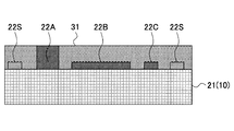
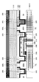
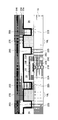
- FIG. 1 is a sectional view showing an example of an electronic component 20 according to the first embodiment
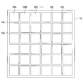
- FIG. 2 is a plan view showing a wafer 10 from which the electronic component 20 of FIG. 1 is cut out.
- the wafer 10 has, for example, a square planar shape, and on the wafer 10, a plurality of electronic component elements 10 ⁇ / b> A, 10 ⁇ / b> B, corresponding to the electronic components 20, respectively. 10C... Are separated by a scribe line 10L and formed in a matrix. 1 is obtained, for example, by dicing any one of the electronic component elements 10A, 10B, 10C,... Formed on the wafer 10 along the scribe line 10L. .
- the wafer is made of, for example, a low-temperature fired ceramic (LTCC) or the like, but can be made of glass, resin, a silicon substrate, or the like.
- LTCC low-temperature fired ceramic
- the electronic component 20 is a MEMS (micro-electromechanical system) switch, which is made of a low-temperature fired ceramic and is formed on a substrate 21 corresponding to the wafer 10.
- a MEMS (micro-electromechanical system) switch which is made of a low-temperature fired ceramic and is formed on a substrate 21 corresponding to the wafer 10.
- a cantilever 23 carrying a contact 23A is formed at the tip portion via a support 22A made of copper (Cu) or the like.
- a contact 22C corresponding to the contact 23A is formed on the surface 21S of the substrate 21, and a drive electrode pattern 22B is formed for driving the cantilever 23 with electrostatic force.
- the contact 22C is actually composed of two contacts 22C 1 and 22C 2 , the cantilever 23 is attracted to the drive electrode pattern 22B, and the contact 23A is contacted with the contacts 22C 1 and 22C 1 . If contact with the 22C 2, for example, high-frequency signal incoming to the contact 22C 1 is output from the contact point 22C 2 conducts the contact 23A.
- the contact 22C includes the contacts 22C 1 and 22C 2 .
- the cantilever 23 is formed of, for example, a silicon oxide film, and carries an upper electrode pattern 23B thereon. Therefore, by applying a driving voltage between the driving electrode pattern 22B and the upper electrode pattern 23B, the cantilever 23 is generated between the driving electrode pattern 22B and the upper electrode pattern 23B. As a result, the contact 23A contacts or leaves the contact 22C.
- an electrode pattern 22D for supplying power to the upper electrode pattern 23B on the cantilever 23 through a bonding wire is formed on the surface 21S of the substrate 21.
- via plugs 21B and 21C are formed in the substrate 21 corresponding to the electrode patterns 22B and 22C, respectively. Although not shown in the cross section of FIG. 1, similar through via plugs are formed in the substrate 21 corresponding to the electrode patterns 22D.
- the through via plugs 21B and 21C, the support 22A, and the upper electrode pattern 23B are made of copper (Cu), for example, and the drive electrode pattern 22B and the contacts 22C and 23A are acid resistant such as gold (Au), for example. It is composed of a changeable metal.
- the support 22A, the electrode patterns 22B and 22D, the cantilever 23 and the contact 22C are continuously surrounded, and made of, for example, gold (Au) or gold / titanium (Au / A seal ring 22S having a Ti) laminated structure or a gold / chrome (Au / Cr) laminated structure is formed in an annular shape.
- a lid member 25 made of, for example, silicon and integrally including a side wall member 25S and a lid member 25C is disposed on the upper surface 21S of the substrate 21.
- the column 22A, the electrode patterns 22B to 22D, the cantilever 23, and the contact point 22C are placed so as to define an operation space 24 in which the contact point 22C is accommodated.
- the lid member 25 has an adhesion layer 25a of, for example, a gold / titanium or gold / chromium laminated structure formed on the entire upper surface thereof, ie, the surface opposite to the substrate 21.
- the side wall member 25S is bonded to the corresponding seal ring 22S via the adhesion layer 25a by placing the lid member 25 on the substrate 21. Further, a shield layer 26 made of, for example, iron-nickel alloy is bonded to the upper surface of the lid member 25.
- the outside of the side wall member 25S is filled with a space between the upper surface 21S of the substrate 21 and the lower surface 26S of the shield layer 26, and is in contact with the adhesion layer 25a covering the side wall surface of the side wall member 25S.
- a sealing member 27 made of tin-bismuth solder is formed.
- the side wall member 25S is further formed with a stepped portion made of a surface 25s facing the upper surface 21S of the substrate 21, and the sealing member 27 is only the side wall surface of the side wall member 25S of the lid member 25.
- the shield layer 26 and the lid member 25 are firmly bonded to the upper surface 21S of the substrate 21 by the sealing member 27.
- the sealing member 27 has a sidewall surface obtained by extending the sidewall surface 21SW of the substrate 21. Note that it is defined by 27SW.
- the sealing member 27 is formed outside the side wall member 25S when viewed from the working space 24.
- the sealing member 27 is bonded to the lid member 25 and the substrate 21, or the shield layer 26 and the substrate.
- the molten sealing member 27 does not flow into the working space 24 in order to promote the joining to the substrate 21.
- a close and strong joint can be realized directly between the seal ring 22S and the lid member 25 or via the sealing member 27, and the size of the working space 24 is made larger than necessary. A desirable feature that there is no need to set can be obtained.
- FIG. 3 is a perspective view showing the main body of the MEMS switch 20 in more detail with the lid member 25, the shield layer 26, and the sealing member 27 removed.
- the electrode pattern 22D is formed on the upper surface 21S of the substrate 21 in the vicinity of the support 22A.
- the electrode pattern 22D is an upper electrode pattern 23B on the cantilever 23. It can be seen that they are connected by a bonding wire 23W. Further, as described above, through electrodes not shown corresponding to the electrode patterns 22D are formed in the substrate 21 in the same manner as the through electrode patterns 21B and 21C.
- the corresponds to the contact 22C has two contacts 22C 1 and 22C 2 is formed, a state where no driving voltage is applied between the electrode pattern 22B and 23B as shown in FIG. 4A in the two contacts 22C 1 and 22C 2 whereas in an electrically non-conductive, said state of Figure 4B where the DC drive voltage from the DC power supply 220 between the electrode pattern 22B and 23B is applied the contact 22C 1 and 22C 2 and conducted through the contact 23A, a high-frequency signal is output to the contact 22C 2, for example the incoming to an input terminal of the contact 22C 1.
- the seal ring 22S and the drive electrode pattern are formed on the surface 21S of the substrate 21 corresponding to the wafer 10.
- 22B and further contacts 22C 1 and 22C 2 are formed to a thickness of 1 ⁇ m, for example, by depositing and patterning a gold film, for example.
- the seal ring 22S is formed with a width of, for example, 150 ⁇ m along a scribe line 10L that defines an element region having a size of, for example, 1500 ⁇ m ⁇ 1000 ⁇ m, and is formed in the element region as described above.
- the pillars 22A, the electrode patterns 22B and 22D, and the contacts 22C 1 and 22C 2 are formed in an annular shape so as to continuously surround the structure.
- the seal ring 22S, the drive electrode pattern 22B, and the contacts 22C 1 and 22C 2 are not shown, but a thin gold film is formed as a seed layer on the surface of the substrate 21, that is, the wafer 10, and each of them is formed thereon.
- a resist film having a resist opening corresponding to the electrode pattern is formed, and the resist film can be formed by an electrolytic plating method using the resist film as a mask.
- a resist film 31 is formed on the substrate 21 so as to cover the structure on the surface 21S. Further, as shown in FIG. 5C, the resist film 31 corresponds to the support 22A. Thus, an opening 31A exposing the surface 21S is formed.
- the support 22A is formed to a height of 8 ⁇ m, for example, as shown in FIG.
- the gold film previously formed on the surface of the wafer 10 in the step of FIG. 5A can be used as a plating seed layer.
- an opening 31B for the contact 23A corresponding to the contacts 22C 1 and 22C 2 is formed to a predetermined depth of 2 ⁇ m, for example, as shown in FIG. 5E.
- a gold pattern filling the opening 31B is formed as the contact 23A to a thickness of 2 ⁇ m.
- the cantilever 23 is formed on the resist film 31 by, for example, a silicon oxide film having a thickness of 5 ⁇ m so as to extend from the support 22A to the contact 23A, and further on the cantilever 23.
- the upper electrode pattern 23B is formed by a copper pattern having a thickness of 0.5 ⁇ m, for example.
- the resist film 31 is dissolved in a solvent or removed by ashing in an oxygen atmosphere, and the upper electrode pattern 23B is not shown in the cross section of FIG. 5I.
- the MEMS switch 20 is formed by connecting the bonding wires 22W as described above with reference to FIG.
- the thin plating seed layer remaining on the surface of the wafer 10 in the step of FIG. 5A is removed by wet etching or the like. Since the plating seed layer is extremely thin, the structure formed in the element region is not substantially affected even when wet etching is performed in this way.
- the main body of the MEMS switch 20 shown in the perspective view of FIG. 3 is formed in all the element regions 10A, 10B, 10C... On the wafer 10 of FIG. It is formed.
- the MEMS switches 20 shown in the perspective view of FIG. 3 are formed in a matrix form on the wafer 10 and separated from each other by a scribe line 10L.
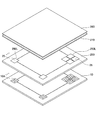
- a cap substrate 250 formed by joining the lid member 25 in a matrix corresponding to the element region on the wafer 10 is bonded onto the wafer 10 and further melted from above the cap substrate 250 to the lower surface.
- the shield substrate 260 carrying the sealant layer 270 such as solder is pressed.
- slit portions 250L corresponding to the scribe lines 10L on the wafer 10 are formed vertically and horizontally so as to surround the lid member 25, and the shield substrate 260 is formed on the cap substrate 250 from above.
- the sealant layer 270 flows under the cap substrate 250 from the slit portion 250L, and is a space between the plurality of MEMS switches 20 having the cross-sectional structure of FIG. Fill.
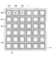
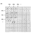
- FIG. 7 is a plan view showing the wafer 10 in the exploded perspective view of FIG.
- a body portion of the MEMS switch 20 shown in the perspective view of FIG. 3 is formed in the plurality of element regions 10A, 10B, 10C,.
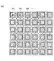
- FIG. 8A is a plan view of the cap substrate 250 in the exploded perspective view of FIG. 6 as viewed from the top, that is, the shield substrate 260 in FIG. 6, and FIG. 8B is the bottom of the cap substrate 250, that is, the wafer 10 in FIG. It is the top view seen from the side.
- the substrate 21 in FIG. 1 is formed by cutting the wafer 10 along the scribe line 10L.
- slits 250L extend vertically and horizontally corresponding to the scribe lines 10L of the wafer 10, and individual lid members 25 are defined.
- each lid member 25 is connected to the adjacent lid member 25 by a rib-like bridge portion 250A.
- Mechanically coupled by 250B the bridging portion 250A couples one lid member 25 to the lid member 25 adjacent in the row direction or the column direction, and the bridging portion 250B couples one lid member 25 to the lid member 25 adjacent in the oblique direction.
- the lower surface of the silicon substrate constituting the cap substrate 250 surrounds a recess corresponding to the working space 24 of FIG. It can be seen that it is formed in a ring shape in the form of a pattern.
- a method for manufacturing such a cap substrate 250 will be described later with reference to FIGS. 11A to 11D.
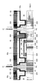
- FIGS. 9A to 9D are cross-sectional views along line AA ′ in FIG. 8A
- FIGS. 10A to 10D are cross-sectional views along line BB ′ in FIG. 8A.
- the adhesion layer 25a is formed on the lower surface of the cap substrate 250, and the side wall member 25S is disposed on the wafer 10 via the adhesion layer 25a.
- the side wall member 25S is disposed so as to contact the seal ring 22S and further presses the cap substrate 250 against the wafer 10 with a pressure of, for example, 1 MPa while being heated to a temperature of, for example, 280 ° C. Even if the seal ring 22S has some unevenness on the surfaces of the side wall member 25S and the seal ring 22S, the seal ring 22S is reliably bonded via the adhesion layer 25a.
- the working space 24 is defined. In the following description, only the working space 24 is illustrated for the element region adjacent to the element region, and the illustration of the MEMS switch 20 main body is omitted.
- a shield substrate 260 carrying a solder layer 270 on the lower surface is disposed on the structure of FIG. 9A.
- the solder layer 270 is melted in an inert atmosphere such as nitrogen, and the shield substrate 260 is pressed in the direction of the arrow, so that the molten solder layer 270 corresponds to the scribe line 10L from the slit 250L. It pushes out into the space 250V formed between each side wall member 25S and 25S between one element area and the adjacent element area.
- the space 250V is connected on the wafer 10, and the nitrogen gas filling the space 250V and excess molten solder pass through the space 250V and pass through the wafer 10.
- the space 250V is filled with the molten solder layer 270.
- the side wall member 25S is joined to the corresponding seal ring 22S in each element region.
- the working space 24 is filled with an inert gas such as nitrogen gas.
- an inert gas such as nitrogen gas.
- the wafer 10 is caused to act along the scribe line 10L, for example, the dicing blade 31 as indicated by an arrow, thereby causing the wafer 10 to move. Is divided into individual element regions, and the MEMS switch 20 described above with reference to FIG. 1 is obtained.
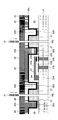
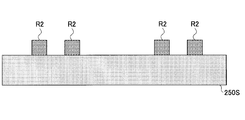
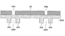
- 11A to 11D are process cross-sectional views illustrating a method for manufacturing the cap substrate 250.
- a resist pattern R1 corresponding to the side wall member 25S shown in the plan view of FIG. 8B is formed on a silicon substrate 250S formed in a square shape corresponding to the wafer 10.
- the silicon substrate 250S is etched to a predetermined depth corresponding to the height of the working space 24, for example, 50 ⁇ m, using the resist pattern R1 as a mask.
- the side wall member 25S is formed on the silicon substrate 250S, and the space 250V is formed between the side wall member 25S defining one element region and the side wall member 25S defining an adjacent element region. Is formed.
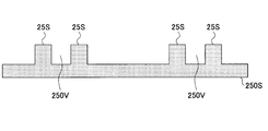
- the silicon substrate 250S in the state of FIG. 11B is turned upside down, and a resist pattern R3 having a resist opening R3A corresponding to the slit 250L is formed on the upper surface, and the resist pattern R3 is further formed.
- the slit 250L is formed in communication with the space 250V as shown in FIG. 11D.
- the process from the surface in which the space 250V is formed is also possible without turning the substrate 250S upside down.
- the silicon substrate 250S in the state of FIG. 11D is turned upside down, and the adhesion layer 25a is formed with a film thickness of, for example, 0.5 ⁇ m on the surface on which the side wall member 25S is formed.
- the cap substrate 250 is formed.
- the cap substrate 250 is formed of the silicon substrate 250S, and the lid member 25 is also formed of silicon. Accordingly, the present embodiment is not limited to such a specific material.
- the cap substrate 250 and the lid member 25 can be made of glass, metal, ceramic, or the like in addition to silicon.
- FIG. 12 is a cross-sectional view showing a configuration of a MEMS switch 20A according to a modification of the present embodiment.
- the same reference numerals are given to the portions corresponding to the previous embodiment, and the description will be omitted.
- a seal ring 32S having a height corresponding to the height of the working space 24 is formed by, for example, electrolytic plating of copper, and the like. Further, the working space 24 is defined by joining a flat lid member 35.
- the flat lid member 35 is made of, for example, silicon and has the same configuration as the lid member 35 made of silicon, but lacks the side wall portion 25S and has a flat lower surface.
- the adhesion layer 25a is formed on the lower surface and the side wall surface of the lid member 35, and the lid member 35 is disposed outside the seal ring 32S constituting the side wall member via a sealing member 27 such as solder.
- the substrate 21 is firmly bonded to the surface 21S.
- the shield layer 26 has an outer shape corresponding to the outer shape of the substrate 21, and the side wall surface defining the outer periphery of the lid member 35 is the side wall surface defining the outer periphery of the shield layer 26. 12 and the side wall surface defining the outer periphery of the seal ring 32S is formed at a position further retracted from the side wall surface of the lid member.
- Two step portions are formed as shown in FIG. In the embodiment of FIG. 12, both of the two stepped portions are filled with solder constituting the sealing portion 27, and as a result, the lid member 35 is firmly bonded to the surface of the substrate 21. .
- FIG. 12 uses a substrate having a flat bottom surface in which the side wall member 25S is not formed in the plan view of FIG. 8B as the cap substrate 250 in the wafer level packaging described with reference to FIG. 9A to 9D and FIGS. 10A to 10D can be formed in the same manner.
- FIG. 13 is a cross-sectional view showing a configuration of a MEMS switch 20B according to another modification of the present embodiment.
- portions corresponding to the previous embodiment are denoted by the same reference numerals, and description thereof is omitted.
- the side wall surface defining the outer periphery of the lid member 35 is the side wall member 32S that also serves as the side wall surface defining the outer periphery of the shield layer 26 that coincides with the outer periphery of the substrate 21 and the seal ring. It should be noted that it is formed at a position that is recessed from any of the side wall surfaces that define the outer periphery.
- a stepped portion filled with the sealing member 27 is formed as shown in the figure, and the shield layer 26 is formed on the substrate 21 by the sealing member 27. Tightly coupled.
- the lid member 35 is firmly coupled to the substrate 11.
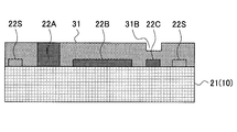
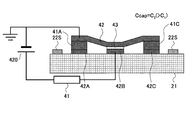
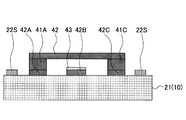
- FIG. 14 is a cross-sectional view showing the configuration of the variable capacitance element 40 according to the second embodiment
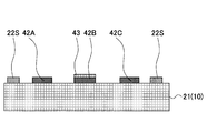
- FIG. 15 is a perspective view showing the configuration of the main body of the variable capacitance element 40 of FIG.
- the cross-sectional view of FIG. 14 shows a cross section taken along line CC ′ in the perspective view of FIG.
- portions corresponding to the portions described above are denoted by the same reference numerals, and description thereof is omitted.
- a ground electrode pattern made of gold instead of the support 22A and the electrode pattern 22C on the substrate 21 corresponding to one element region of the wafer 10.
- 42A and 42C are formed, respectively, and pillars 41A and 41C made of copper are formed on the ground electrode patterns 42A and 42C, for example, at a height of 2 ⁇ m.
- An upper electrode pattern 42 of an air bridge structure made of a gold film is formed between the support posts 41A and 41C with a film thickness of, for example, 1 ⁇ m.
- a lower electrode pattern 42B is formed to face the upper electrode 42.
- the upper electrode pattern 42 is provided so as to be displaceable with respect to the opposed lower electrode pattern 42B, and the upper electrode pattern 42 and the lower electrode pattern 42B constitute a variable capacitance element.
- a capacitor dielectric film 43 made of a silicon oxide film or the like is formed on the lower electrode pattern 42B so that the upper electrode pattern 42 and the lower electrode pattern 42B are not short-circuited.
- the seal ring 22S defines an element region on the substrate 21 as in the previous embodiment, and the lower electrode pattern 42B is on the surface 21S of the substrate 21. It can be seen that it extends under the upper electrode pattern 42 from the high frequency signal input side (RFin) to the high frequency signal output side (RFout). Also in the substrate 21, the via plug 21B 1 and 21B 2 shown in cross section in FIG. 14, it is formed to correspond to and the output side to each of the input side.
- the seal ring 22S and the electrode patterns 42A and 42C are grounded via through via plugs 21A and 21C formed in the substrate 21, respectively (GND).
- the variable capacitance element 40 is connected to a high-frequency transmission path formed by the lower electrode pattern 42B by a capacitance Ccap formed between the upper electrode pattern 42 and the lower electrode pattern 42B. An element having the above structure is formed.
- FIG. 16A and 16B are diagrams for explaining the operation of the variable capacitance element 40.
- FIG. 16A and 16B are diagrams for explaining the operation of the variable capacitance element 40.
- variable capacitance element 40 by applying a DC voltage between the upper electrode 42 and the lower electrode 42B, the lower electrode pattern 42B is formed as shown in the equivalent circuit diagram of FIG. 16C.
- the capacitance of the capacitor connected to the transmission path of the high frequency signal to be configured can be changed.
- the adhesion layer 25 a having an Au / Ti laminated structure is removed from the portion of the lid member 25 facing the substrate 21 in the working space 24. It should be noted that. According to this configuration, no parasitic capacitance is generated between the electrode pattern to which a high frequency signal is supplied on the substrate 21 and the lid member 25, and the influence of the parasitic capacitance on the operation of the variable capacitance element 40 is suppressed. can do.
- variable capacitance element 40 of FIG. 14 will be described.
- the seal ring 22S and the ground electrode pattern are formed on the surface 21S of the substrate 21 corresponding to the wafer 10.
- 42A, 42C and the lower electrode pattern 42B are formed to a thickness of 1 ⁇ m, for example, by depositing and patterning a gold film, for example.
- the seal ring 22S is formed with a width of, for example, 150 ⁇ m along the scribe line 10L that defines an element region having a dimension of, for example, 1500 ⁇ m ⁇ 1000 ⁇ m.
- the electrode patterns 42A to 42C and the like formed in the element region are formed in an annular shape so as to continuously surround the structure.
- a thin gold film that is not shown in the drawing and serves as a plating seed layer is formed on the surface 21S of the substrate 21, and thus on the surface of the wafer 10.
- the seal ring 22S and the electrode patterns 42A to 42C are formed by electrolytic plating using a resist pattern formed on the plating seed layer and having a resist opening corresponding to each of the electrode patterns 42A to 42C as a mask.
- a dielectric film such as a silicon oxide film is formed on the substrate 21 and further patterned by a resist process (not shown), thereby forming the dielectric film on the lower electrode pattern 42B as shown in FIG. 17B.
- a capacitor insulating film 43 made of, for example, a silicon oxide film is formed.
- a resist film 45 is formed on the substrate 21 so as to cover the seal ring 22S and the electrode patterns 42A to 42C, and further, the ground electrode is formed in the resist film 45 as shown in FIG. 17D.
- openings 45A and 45C are formed so as to expose the ground electrode patterns 42A and 42C.
- a copper film is formed on the ground electrode patterns 42A and 42C so as to fill the resist openings 45A and 45C.
- a support post 41A made of copper and a support post 41C made of copper are formed on the ground electrode pattern 42C by electrolytic plating.
- the gold film previously formed on the surface of the wafer 10 in the step of FIG. 17A can be used as a plating seed layer.
- a gold film is formed on the resist film 45 by a low temperature process such as sputtering, and further patterned to form an upper electrode pattern 42 that bridges the support columns 41A and 41C.
- the resist film 45 is dissolved in a solvent or the like, or is removed by ashing in an oxygen atmosphere, whereby the variable capacitance element 40 of FIG. 14 is formed.
- the seal ring 22S, the electrode patterns 22B, 22C, etc. are formed by the electrolytic plating method in the process of FIG. 17A, the plating seed layer remaining on the surface of the wafer 10 is After the resist film 45 is removed, the resist film 45 is removed by wet etching or the like.
- variable capacitance element 40 is formed in each of the element regions 10A, 10B, 10C,..., FIGS. 6, 7, 8A to 8B, and 9A to 9D are previously described.
- the variable capacitance element 40 shown in FIG. 14 is completed.
- the adhesive layer 25a is removed from the lower surface of the lid member 25 made of silicon in order to reduce parasitic capacitance. Should.
- the process of FIGS. 18A and 18B is further performed following the process of FIG.
- the adhesion layer 25 a is removed from the portion of the substrate 250 that faces the surface 21 ⁇ / b> S of the substrate 21 when the lid member 25 is mounted on the substrate 21.
- a resist pattern R4 is formed on the silicon substrate 250S constituting the cap substrate 250 so as to cover the slit portion 250L and the side wall member 25S, and further, the silicon substrate using the resist pattern R4 as a mask.
- the adhesion layer 25a exposed on 250S is removed by, for example, sputter etching or wet etching.
- variable capacitor 40 having the structure described above with reference to FIG. 14 can be obtained.
- the lid member 25, and thus the cap substrate 250 is not limited to silicon, but can be formed of an insulating material such as glass or ceramic.
- the lid member 25, and hence the cap substrate 250 is formed of silicon, it is preferable to use an insulating silicon substrate having a specific resistance of 1000 ⁇ cm or more.
- FIG. 19 is a cross-sectional view showing a configuration of a variable capacitor 40A according to a modification of the present embodiment.
- the same reference numerals are assigned to portions corresponding to the previous embodiment, and the description thereof is omitted.
- a seal ring 32 ⁇ / b> S having a height corresponding to the height of the working space 24 is replaced with, for example, copper.
- the working space 24 is defined by joining a flat lid member 35 thereon.
- the flat lid member 35 is made of, for example, silicon and has the same configuration as the lid member 35 made of silicon, but lacks the side wall portion 25S and has a flat lower surface.
- the adhesion layer 25a is formed on the lower surface and the side wall surface of the lid member 35, and the lid member 35 is disposed outside the seal ring 32S constituting the side wall member via a sealing member 27 such as solder.
- the substrate 21 is firmly bonded to the surface 21S.
- the shield layer 26 has an outer shape corresponding to the outer shape of the substrate 21, and the side wall surface defining the outer periphery of the lid member 35 is the side wall surface defining the outer periphery of the shield layer 26. 19 and the side wall surface defining the outer periphery of the seal ring 32S is formed at a position further retracted from the side wall surface of the lid member.
- Two step portions are formed as shown in FIG. In the embodiment of FIG. 19, both of the two stepped portions are filled with solder constituting the sealing portion 27, and as a result, the lid member 35 is firmly bonded to the surface of the substrate 21. .
- FIG. 19 uses a substrate having a flat bottom surface in which the side wall member 25S is not formed in the plan view of FIG. 8B as the cap substrate 250 in the wafer level packaging described with reference to FIG. 9A to 9D and FIGS. 10A to 10D can be formed in the same manner.
- FIG. 20 is a cross-sectional view showing a configuration of a variable capacitor 40B according to another modification of the present embodiment.
- parts corresponding to those of the previous embodiment are denoted by the same reference numerals, and description thereof is omitted.
- the side wall surface that defines the outer periphery of the lid member 35 is the side wall member 32 ⁇ / b> S that also functions as the side wall surface that defines the outer periphery of the shield layer 26 that coincides with the outer periphery of the substrate 21. It should be noted that it is formed at a position that is recessed from any of the side wall surfaces that define the outer periphery.
- a stepped portion filled with the sealing member 27 is formed as shown in the figure, and the shield layer 26 is formed on the substrate 21 by the sealing member 27. Tightly coupled.
- the lid member 35 is firmly coupled to the substrate 11.
- the size of the lid member 35 is reduced, and the variable capacitance element 40B can be further downsized.
- the sealing member 27 is not limited to solder, and for example, a resin can be used. By using a resin as the sealing member 27, the electronic component can be reduced in weight.
- the element formed in the working space 24 is not limited to a MEMS switch or a variable capacitance element, and it is also possible to form a crystal resonator, for example.
Landscapes
- Engineering & Computer Science (AREA)
- Microelectronics & Electronic Packaging (AREA)
- Manufacturing & Machinery (AREA)
- Physics & Mathematics (AREA)
- Acoustics & Sound (AREA)
- Computer Hardware Design (AREA)
- Mechanical Engineering (AREA)
- Micromachines (AREA)
Abstract
電子部品は、基板と、前記基板上に形成された素子と、前記基板上において前記素子を囲む側壁部材と、前記側壁部材上に配設され、前記側壁部材と共に、前記基板上において前記素子を囲む空間を画成する蓋部材と、前記側壁部材の外側に設けられ、前記側壁部材および蓋部材を前記基板の表面に接合し、前記空間を封止する封止部材と、を備える。
Description
以下に説明する実施形態は、電子部品およびその製造方法に関する。
ウェハレベルパッケージ技術は、半導体ウェハ上に形成された多数の素子を、半導体ウェハを個々のチップに分割する前に一括して封止する技術であり、費用が安く、また得られる電子素子を大略、個々のチップのサイズに形成できることから、小型の半導体装置の製造に広く使われている。
一方、最近では、ウェハ上に可動部を有するスイッチや容量可変キャパシタ、水晶振動子などの電子部品を一括して形成する試みがなされている。そこで、このような電子部品素子の製造においても、これらウェハ上に上記電子部品に対応して形成された電子部品素子を、ウェハレベルパッケージ技術により封止し、電子部品の小型化と製造費用の低減を図りたいとの要望がある。
例えば電子部品が可動部を有するものである場合、電子部品に対応してウェハ上に形成された素子を封止しようとすると、当該素子を覆う蓋部材をウェハ上に、前記蓋部材が前記ウェハ上において前記素子を囲む空間を画成するように封止するのが望ましい。
例えば特許文献1においては素子がウェハ表面の凹部に形成され、蓋部材を前記ウェハの表面にロウ材を介して接合することにより、前記素子を封止する方法が開示されている。また特許文献2においては、蓋部材がウェハ上に素子を囲んで形成された外周壁部材の上面にロウ材層を介して接合され、これにより前記素子の封止がなされている。
このように蓋部材をウェハ表面、あるいはウェハ表面上に形成された外周壁部材の上面にロウ材層を介して接合する場合には、ロウ材層を溶融させる必要があり、また溶融したロウ材層が基板表面や蓋部材表面の凹凸を吸収することで確実な封止が得られるように、蓋部材を軽く押圧するのが好ましい。しかし、溶融したロウ材層を圧迫すると、ロウ材が前記素子を囲む空間に流れ出す、あるいは押し出されてしまうおそれがある。流れ出したロウ材が素子に接触すると、電気的な不良を引き起こすのみならず、特に可動部を有する素子の場合、前記可動部の動作が妨げられてしまう。
そこで、このような従来の構成では、前記空間の寸法を、このようなロウ材の流入を考慮して必要以上に大きく設定する必要があり、電子部品の寸法の増大を招いていた。
特開平11-340350号公報
特開2006-74291号公報
一の側面によれば電子部品は、基板と、前記基板上に形成された素子と、前記基板上において前記素子を囲む側壁部材と、前記側壁部材上に配設され、前記側壁部材と共に、前記基板上において前記素子を囲む空間を画成する蓋部材と、前記側壁部材の外側に設けられ、前記側壁部材および蓋部材を前記基板の表面に接合し、前記空間を封止する封止部材と、を備える。
他の側面によれば電子部品の製造方法は、ウェハ上に複数の素子を行列状に形成する工程と、前記複数の素子にそれぞれ対応した複数の蓋部材が行列状に形成され、それぞれの蓋部材が対応する素子を囲む側壁部を含み、また隣接する蓋部材どうしが溝部で相互に隔てられ、かつ隣接する蓋部材どうしが前記溝部を架橋する架橋部により相互に結合した状態で形成されたキャップ基板を作製する工程と、前記キャップ基板を前記ウェハ上に、それぞれの蓋部材において側壁部が対応する素子を囲むように載置する工程と、前記キャップ基板上に流動状態の封止層を担持したシールド基板を押圧し、前記溝部を介して、前記それぞれの素子を囲む側壁部の外側に圧入し、固化させることにより、前記シールド基板の下方において隣接する側壁部の間を封止部材で充填する工程と、前記シールド基板、前記キャップ基板および前記ウェハを前記溝部に沿って切断し、前記複数の素子を個々の電子部品に分離させる工程と、を含む。
他の側面によれば電子部品の製造方法は、ウェハ上に複数の素子を行列状に形成する工程と、前記ウェハ上に、前記複数の素子をそれぞれ囲むように、前記ウェハの表面から屹立する複数の側壁部材をシールリングとして形成する工程と、前記複数の素子にそれぞれ対応した複数の蓋部材が行列状に形成され、隣接する蓋部材どうしが溝部で相互に隔てられ、かつ隣接する蓋部材どうしが前記溝部を架橋する架橋部により相互に結合した状態で形成されたキャップ基板を作製する工程と、前記キャップ基板を前記ウェハ上に、それぞれの蓋部材が対応する素子を覆い、また対応する側壁部材に係合するように載置する工程と、前記キャップ基板上に流動状態の封止層を担持したシールド基板を押圧し、前記溝部を介して、前記それぞれの素子を囲む側壁部材の外側に圧入し、固化させることにより、前記シールド基板の下方において隣接する側壁部材の間を封止部材で充填する工程と、前記シールド基板、前記キャップ基板および前記ウェハを前記溝部に沿って切断し、前記複数の素子を個々の電子部品に分離させる工程と、を含む。
基板上の素子を蓋部材および側壁部材で囲み、側壁部材の外側において当該側壁部材および蓋部材を封止部材により基板表面に結合し素子を封止することにより、封止部材の素子が形成されている空間へのはみ出しを回避することが可能となる。
10 ウェハ
10A,10B,10C 素子領域
10L スクライブライン
20 MEMSスイッチ
21 基板
21A~21C,21B1,21B2 貫通ビアプラグ
21S 基板表面
21SW 基板側壁面
22A 支柱
22B 駆動電極パターン
22C,22C1,22C2,23A 接点
22D 電極パターン
22S シールリング
220,420 直流電圧源
23 カンチレバー
23B 上部電極パターン
23W ボンディングワイヤ
24 作動空間
25 蓋部材
25S 側壁部材
25a 密着層
250 キャップ基板
250A,250B 架橋部
250L スリット部
250V 空間
26 シールド層
26S シールド層下面
260 シールド基板
27 封止部材
27SW 封止部材側壁面
270 封止材層
31,45 レジスト膜
31A,31B,45A,45C レジスト開口部
[第1の実施形態]
[第1の実施形態]
図1は、第1の実施形態による電子部品20の例を示す断面図,図2は図1の電子部品20が切り出されるウェハ10を示す平面図である。
[第1の実施形態]
図1は、第1の実施形態による電子部品20の例を示す断面図,図2は図1の電子部品20が切り出されるウェハ10を示す平面図である。
まず図2の平面図を参照するに、前記ウェハ10は例えば正方形の平面形状を有しており、前記ウェハ10上には、前記電子部品20にそれぞれ対応する複数の電子部品要素10A,10B,10C・・・が、スクライブライン10Lにより隔てられて、行列状に形成されている。図1の電子部品20は、例えば前記ウェハ10上に形成された電子部品要素10A,10B,10C・・・のいずれかを、前記スクライブライン10Lに沿ってダイシングすることにより得られたものである。前記ウェハは例えば低温焼成セラミック(LTCC)などより構成されるが、ガラスや樹脂、シリコン基板などより構成することも可能である。
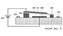
次に図1の断面図を参照するに、図示の例では電子部品20はMEMS(micro-electromechanical system)スイッチであり、低温焼成セラミックよりなり前記ウェハ10に対応する基板21上に形成されており、前記基板21の表面21S上には銅(Cu)などよりなる支柱22Aを介して、先端部に接点23Aを担持するカンチレバー23が形成されている。また前記基板21の表面21S上には、前記接点23Aに対応する接点22Cが形成され、さらに前記カンチレバー23を静電気力で駆動するために駆動電極パタ―ン22Bが形成されている。後で説明するように、前記接点22Cは実際には二つの接点22C1,22C2より構成されており、前記カンチレバー23が駆動電極パタ―ン22Bに吸引されて前記接点23Aが接点22C1,22C2にコンタクトした場合、例えば前記接点22C1に入来した高周波信号が、前記接点23Aを導通して接点22C2から出力される。以下における図1の断面図の説明では、前記接点22Cは前記接点22C1,22C2を包含するものとする。
前記カンチレバー23は、例えばシリコン酸化膜などより形成され、その上に上部電極パタ―ン23Bを担持している。そこで、前記駆動電極パタ―ン22Bと上部電極パタ―ン23Bの間に駆動電圧を印加することにより、前記カンチレバー23は、前記駆動電極パタ―ン22Bと上部電極パタ―ン23Bの間に生じた電磁力による駆動され、その結果、前記接点23Aが前記接点22Cにコンタクトしたり離れたりする。
また図1の断面には図示されないが、前記基板21の表面21S上には、前記カンチレバー23上の上部電極パターン23Bにボンディングワイヤを介して給電するための電極パタ―ン22Dが形成されている。図1のMEMSスイッチ20本体のより詳細な説明は、後で図3の斜視図を参照しながら行う。
前記基板21中にはさらに、前記電極パタ―ン22B,22Cにそれぞれ対応して貫通ビアプラグ21B,21Cがそれぞれ形成されている。図1の断面には図示されないが、同様な貫通ビアプラグが、前記基板21中に、前記電極パタ―ン22Dに対応して形成されている。
一例によれば、前記貫通ビアプラグ21B,21C、支柱22A、上部電極パタ―ン23Bは例えば銅(Cu)より構成され、前記駆動電極パターン22B,接点22C,23Aは例えば金(Au)などの耐酸化性金属により構成される。
さらに前記基板21の表面21S上には、前記支柱22Aおよび電極パタ―ン22B,22D、カンチレバー23および接点22Cを連続的に囲んで、例えば金(Au)よりなる、あるいは金/チタン(Au/Ti)積層構造、あるいは金/クロム(Au/Cr)積層構造を有するシールリング22Sが環状に形成されている。
前記シールリング22S上には、例えばシリコンよりなり、側壁部材25Sと蓋部材25Cとを一体的に有する蓋部材25が、前記基板21の上面21S上に、前記支柱22A、電極パタ―ン22B~22Dおよびカンチレバー23、さらに前記接点22Cなどが収納される作動空間24を画成するように載置される。図示の実施形態では前記蓋部材25は、その上面、すなわち前記基板21とは反対の側の面を除いて全面に、例えば金/チタンあるいは金/クロム積層構造の密着層25aが形成されており、前記側壁部材25Sは、前記蓋部材25を前記基板21上に載置することにより、対応するシールリング22Sに、かかる密着層25aを介して接合されている。また前記蓋部材25には、その上面に、例えば鉄ニッケル合金などよりなるシールド層26が接合されている。
さらに前記側壁部材25Sの外側には、前記基板21の上面21Sと前記シールド層26の下面26Sの間の空間を充填して、また前記側壁部材25Sの側壁面を覆う密着層25aに接して、例えばスズビスマス系のはんだよりなる封止部材27が形成されている。図示の例では、前記側壁部材25Sには、前記基板21の上面21Sに対面する面25sよりなる段差部がさらに形成され、前記封止部材27は前記蓋部材25の側壁部材25Sの側壁面のみならず、かかる段差部にも接合していることに注意すべきである。その結果、前記シールド層26および前記蓋部材25は前記封止部材27により、前記基板21の上面21Sにしっかりと接合される。
また本実施形態では、後で詳細に説明するように、ウェハレベルパッケージングに引き続き実行されるダイシング工程が行われる結果、前記封止部材27は、前記基板21の側壁面21SWを延長した側壁面27SWにより画成されていることに注意すべきである。
本実施形態によれば、前記封止部材27は、前記作動空間24から見て前記側壁部材25Sの外側に形成されるため、例えば蓋部材25および基板21に対する接合、あるいは前記シールド層26および基板21に対する接合を促進すべく、例えば前記封止部材27が溶融した状態で前記蓋部材25を基板21に対して押圧しても、溶融した封止部材27が前記作動空間24に流入することはなく、前記シールリング22Sと蓋部材25との間に直接に、また前記封止部材27を介しても、密接で強固な接合を実現でき、さらに前記作動空間24の大きさを必要以上に大きく設定する必要がないという、好ましい特徴を得ることが出来る。
図3は、前記MEMSスイッチ20の本体部を、前記蓋部材25およびシールド層26,封止部材27を除去した状態でより詳細に示す斜視図である。
図3を参照するに、前記基板21の上面21S上には前記支柱22Aの近傍に前記電極パタ―ン22Dが形成されており、前記電極パタ―ン22Dは前記カンチレバー23上の上部電極パターン23Bにボンディングワイヤ23Wにより接続されているのがわかる。また先に説明したように前記基板21中には、前記電極パターン22Dに対応して図示していない貫通電極が、前記貫通電極パターン21B,21Cと同様に形成されている。
図3の構成では、前記接点22Cに対応して二つの接点22C1および22C2が形成されており、図4Aに示すように前記電極パターン22Bと23Bの間に駆動電圧が印加されていない状態では前記二つの接点22C1および22C2は電気的に非導通であるのに対し、前記電極パターン22Bと23Bの間に直流電源220から直流の駆動電圧が印加されている図4Bの状態では前記接点22C1および22C2とは前記接点23Aを介して導通し、例えば前記接点22C1の入力端子に入来した高周波信号が接点22C2へと出力される。
以下、図1のMEMSスイッチ20の製造方法を説明する。
最初に、前記MEMSスイッチ20の本体部の製造について、図5A~図5Iを参照しながら簡単に説明する。
図5Aを参照するに、最初に図2のウェハ10の各々の素子領域10A,10B,10C・・・において、前記ウェハ10に対応する基板21の表面21S上に、シールリング22Sおよび駆動電極パターン22B、さらに接点22C1,22C2が、例えば金膜の堆積およびパターニングにより、例えば1μmの厚さに形成される。ここで前記シールリング22Sは例えば各々1500μm×1000μmの寸法の素子領域を画成するスクライブライン10Lに沿って、例えば150μmの幅で形成されており、先にも述べたように当該素子領域に形成される支柱22Aや電極パターン22B,22D、接点22C1,22C2などの構造を連続して囲むように環状に形成される。
例えば前記シールリング22Sおよび駆動電極パターン22B、さらに接点22C1,22C2は、図示は省略するが、前記基板21、すなわちウェハ10の表面に薄い金膜をシード層として形成し、その上にそれぞれの電極パターンに対応したレジスト開口部を有するレジスト膜を形成し、前記レジスト膜をマスクとした電解メッキ法などにより形成することができる。
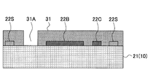
次に図5Bに示すように前記基板21上に、前記表面21S上の構造を覆って、レジスト膜31が形成され、さらに図5Cに示すように前記レジスト膜31中に、前記支柱22Aに対応して前記表面21Sを露出する開口部31Aが形成される。
さらに前記開口部31Aにおいて銅層を例えば電解メッキ法により堆積することにより、前記支柱22Aが図5Dに示すように、例えば8μmの高さに形成される。ここで、前記支柱22A,22Cを電解メッキにより形成するにあたっては、先に図5Aの工程で前記ウェハ10の表面に形成してあった金膜を、メッキシード層として使うことができる。
さらに前記レジスト膜31中には前記接点22C1,22C2に対応して図5Eに示すように前記接点23Aのための開口部31Bが所定の例えば2μmの深さに形成され、さらに図5Fに示すように前記開口部31Bを充填して金パタ―ンが、前記接点23Aとして、2μmの厚さに形成される。
さらに図5Gに示すように前記レジスト膜31上に、前記支柱22Aから接点23Aまで延在するように、例えば厚さが5μmのシリコン酸化膜により、前記カンチレバー23が形成され、さらに前記カンチレバー23上に、図5Hに示すように例えば厚さが0.5μmの銅パタ―ンにより、前記上部電極パターン23Bを形成する。
さらに図5Iに示すように前記レジスト膜31を溶媒などに溶解させることにより、あるいは酸素雰囲気中でのアッシングにより除去し、前記上部電極パターン23Bを図5Iの断面には示されていない電極パターン22Dに、ボンディングワイヤ22Wにより、先に図3で説明したように接続することにより、MEMSスイッチ20が形成される。
また図5Iの工程では、先に図5Aの工程で前記ウェハ10の表面に形成されたまま残っている薄いメッキシード層が、ウェットエッチングなどにより除去される。メッキシード層は極めて薄いため、このようにウェットエッチングを行っても、前記素子領域に形成された構造は、実質的な影響を受けない。
このようにして図5A~図5Iの工程により、前記図2のウェハ10上のすべての素子領域10A,10B,10C・・・において、前記図3の斜視図に示すMEMSスイッチ20の本体部が形成される。
なお前記基板21中には、図5Aの工程の段階で、前記貫通ビアプラグ21B,21Cなどはすでに形成されているものとする。
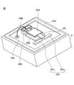
次に、このようなウェハ10に対して行われる第1の実施形態によるウェハレベルパッケージングについて、まず概要を図6の分解斜視図を参照しながら説明する。
図6を参照するに、前記ウェハ10上にはそれぞれの素子領域に前記図3の斜視図に示したMEMSスイッチ20が、スクライブライン10Lにより相互に隔てられて行列状に形成されており、前記ウェハ10上には、前記蓋部材25を、前記ウェハ10上の素子領域に対応して行列状に結合して形成したキャップ基板250が接合され、さらに前記キャップ基板250の上方から、下面に溶融はんだなどの封止剤層270を担持したシールド基板260が押圧される。
前記キャップ基板250には、前記ウェハ10上のスクライブライン10Lに対応したスリット部250Lが、前記蓋部材25を囲むように縦横に形成されており、前記シールド基板260を前記キャップ基板250に上方から押圧すると前記封止剤層270は前記スリット部250Lから前記キャップ基板250の下に流入し、前記ウェハ10上に形成されている前記図1の断面構造を有する多数のMEMSスイッチ20の間の空間を充填する。
図7は、図6の分解斜視図におけるウェハ10を示す平面図である。
図7を参照するに、前記ウェハ10上には、前記図2の平面図に対応して素子領域10A,10B,10C・・・が、縦横に延在する幅が例えば110μmのスクライブライン10Lにより画成されており、前記複数の素子領域10A,10B,10C・・・にはシールリング22Sに囲まれて、前記図3の斜視図に示したMEMSスイッチ20の本体部が形成されている。
図8Aは、前記図6の分解斜視図におけるキャップ基板250を上面、すなわち図6におけるシールド基板260の側から見た平面図、図8Bは前記キャップ基板250を下面、すなわち図6におけるウェハ10の側から見た平面図である。前記ウェハ10を前記スクライブライン10Lに沿って切断することにより、図1における基板21が形成される。
図8Aの平面図を参照するに、前記キャップ基板250を構成するシリコン基板中には、前記ウェハ10のスクライブライン10Lに対応してスリット250Lが縦横に延在し、個々の蓋部材25を画成しており、また個々の蓋部材25は隣接する蓋部材25に、リブ状の架橋部250A.250Bにより、機械的に結合されている。このうち架橋部250Aは一つの蓋部材25を、行方向あるいは列方向に隣接する蓋部材25に結合し、架橋部250Bは一つの蓋部材25を斜め方向に隣接する蓋部材25に結合する。
また図8Bの平面図を参照するに、キャップ基板250を構成する前記シリコン基板の下面には、前記図1の作動空間24に対応する凹部を囲んで、各々の素子領域に側壁部材25Sが凸パタ―ンの形で環状に形成されているのがわかる。
このようなキャップ基板250の製造方法については、後で図11A~図11Dを参照しながら説明する。
次に、本実施形態によるウェハレベルパッケージングのより詳細な説明を、図9A~図9Dおよび図10A~図10Dの工程断面図を参照しながら行う。ただし図9A~図9Dは図8A中、線A-A'に沿った断面図であり、図10A~図10Dは図8A中、線B-B'に沿った断面図である。
図9Aおよび図10Aを参照するに、前記キャップ基板250の下面には前記密着層25aが形成され、前記キャップ基板250は、前記ウェハ10上に、前記側壁部材25Sが前記密着層25aを介して前記シールリング22Sにコンタクトするように配設され、さらに例えば280℃の温度に加熱しながら前記ウェハ10に対して前記キャップ基板250を例えば1MPaの圧力で押圧することにより、前記側壁部材25Sが前記シールリング22Sに、前記側壁部材25Sおよび前記シールリング22Sの表面に多少の凹凸があったとしても、前記密着層25aを介して確実に接合される。前記側壁部材25Sが各々の素子領域10A,10B,10C・・・においてそれぞれのシールリング22Sと接合する結果、前記各々の素子領域10A,10B,10C・・・には、前記側壁部材25Sにより囲まれて、前記作動空間24が画成されている。なお以下の説明では、当該素子領域に隣接する素子領域については、作動空間24のみを図示し、MEMSスイッチ20本体の図示は省略する。
次に図9Bおよび図10Bに示すように、前記図9Aの構造上に、下面にハンダ層270を担持したシールド基板260を配設し、さらに図9Cおよび図10Cに示すように、前記ハンダ層270を、例えば窒素などの不活性雰囲気中において溶融させ、さらに前記シールド基板260を矢印の方向に押圧することにより、前記溶融ハンダ層270を前記スリット250Lから、前記スクライブライン10Lに対応して、一の素子領域と隣接する素子領域の間においてそれぞれの側壁部材25Sと25Sの間に形成される空間250Vに押し出す。前記空間250Vは図8Bの平面図からわかるように前記ウェハ10上において連結しており、前記空間250Vを充填していた窒素ガスや、余分の溶融ハンダは、前記空間250Vを通って前記ウェハ10の外部へと排出され、前記空間250Vは前記溶融ハンダ層270により充填される。
図9Cおよび図10Cの状態では、前記側壁部材25Sがそれぞれの素子領域において、対応するシールリング22Sに接合されている結果、前記作動空間24は窒素ガスなどの不活性ガスが充填された状態で密閉されており、前記シールド基板260を押圧しても、前記溶融ハンダ層270が作動空間24に流入することはない。このため本実施形態では、前記作動空間24を、それぞれの素子領域におけるカンチレバー23などの寸法に対して、溶融はんだ層270の流入を勘案して過大に設定する必要がなく、MEMSスイッチ20を小型に形成することが可能となる。
さらに前記溶融ハンダ層270を固化させた後、図9Dおよび図10Dに示すように前記ウェハ10をスクライブライン10Lに沿って、例えばダイシングブレード31を矢印で示すように作用させることにより、前記ウェハ10は個々の素子領域に分割され、先に図1で説明したMEMSスイッチ20が得られる。
さらに図11A~図11Dは、前記キャップ基板250の製造方法を説明する工程断面図である。
図11Aを参照するに、例えば前記ウェハ10に対応して正方形形状に形成されたシリコン基板250S上に、図8Bの平面図に示された側壁部材25Sに対応してレジストパターンR1が形成され、図11Bに示すように前記シリコン基板250Sを、前記レジストパターンR1をマスクに、前記作動空間24の高さに対応する所定の深さ、例えば50μmまで、エッチングする。かかるエッチングの結果、前記シリコン基板250Sには前記側壁部材25Sが形成され、また一の素子領域を画成する側壁部材25Sと隣接する素子領域を画成する側壁部材25Sとの間に前記空間250Vが形成される。
さらに図11Cに示すように前記図11Bの状態のシリコン基板250Sを上下反転させ、さらに上面に、前記スリット250Lに対応したレジスト開口部R3Aを有するレジストパターンR3を形成し、さらに前記レジストパターンR3をマスクに前記シリコン基板250をエッチングすることにより、図11Dに示すように、前記空間250Vに連通して前記スリット250Lを形成する。
なお基板250Sの上下反転無しで、空間250Vを形成した面からの加工も可能である
さらに図11Eに示すように前記図11Dの状態のシリコン基板250Sを上下反転させ、前記側壁部材25Sが形成されている側の面に前記密着層25aを、例えば0.5μmの膜厚で形成することにより、前記キャップ基板250が形成される。
さらに図11Eに示すように前記図11Dの状態のシリコン基板250Sを上下反転させ、前記側壁部材25Sが形成されている側の面に前記密着層25aを、例えば0.5μmの膜厚で形成することにより、前記キャップ基板250が形成される。
このように本実施形態では前記キャップ基板250をシリコン基板250Sより形成しており、これに伴い蓋部材25もシリコンより構成されるが、本実施形態はかかる特定の材料に限定されるものではなく、前記キャップ基板250および蓋部材25は、シリコン以外にガラスや金属、セラミックなどより構成することも可能である。
図12は、本実施形態の一変形例によるMEMSスイッチ20Aの構成を示す断面図である。ただし図12中、先の実施形態に対応する部分には同一の参照符号を付し、説明を省略する。
図12を参照するに、本実施形態では前記シールリング22Sの代わりに、前記作動空間24の高さに対応する高さを有するシールリング32Sを、例えば銅の電解メッキなどにより形成し、その上に、平板状の蓋部材35を接合することにより、前記作動空間24を画成している。前記平板状の蓋部材35は例えばシリコンよりなり、シリコンよりなる前記蓋部材35と同様の構成を有しているが、前記側壁部25Sを欠いており、平坦な下面を有している。
前記蓋部材35の下面および側壁面には前記密着層25aが形成されており、前記蓋部材35は、側壁部材を構成するシールリング32Sの外側において、ハンダなどの封止部材27を介して前記基板21の表面21Sに強固に接合される。
図12の例では前記シールド層26が前記基板21の外形に対応した外形を有しており、前記蓋部材35の外周を画成する側壁面は前記シールド層26の外周を画成する側壁面から後退して形成されており、また前記シールリング32Sの外周を画成する側壁面は、前記蓋部材の側壁面からさらに後退した位置に形成されているため、図12の構成では、図中に囲んでしめしたように二つの段差部が形成される。図12の実施形態では、上記二つの段差部は、いずれも前記封止部27を構成するハンダにより充填されており、その結果、前記蓋部材35は前記基板21の表面に強固に結合される。
図12の構成は、先に図6で説明したウェハレベルパッケージングの際に、前記キャップ基板250として、図8Bの平面図において前記側壁部材25Sを形成していない、下面が平坦な基板を使って、前記図9A~図9Dおよび図10A~図10Dのプロセスを実行することにより、同様に形成することができる。
図13は、本実施形態の他の変形例によるMEMSスイッチ20Bの構成を示す断面図である。ただし図13中、先の実施形態に対応する部分には同一の参照符号を付し、説明を省略する。
図13の変形例では、前記蓋部材35の外周を画成する側壁面が、前記基板21の外周と一致するシールド層26の外周を画成する側壁面およびシールリングを兼用する前記側壁部材32Sの外周を画成する側壁面のいずれよりも後退した位置に形成されていることに注意すべきである。
かかる構成の結果、図13の変形例では、図中に囲んで示したように封止部材27により充填された段差部が形成され、前記シールド層26が前記基板21に前記封止部材27により強固に結合される。その結果、図13の変形例においても、前記蓋部材35は前記基板11に強固に結合される。
また図13の構成では、前記蓋部材35の寸法が縮小され、MEMSスイッチ20Bをさらに小型化することが可能である。
[第2の実施形態]
図14は、第2の実施形態による可変容量素子40の構成を示す断面図、図15は前記図14の可変容量素子40の本体部の構成を示す斜視図である。図14の断面図は、図15の斜視図中、線C-C'に沿った断面を示している。図中、先に説明した部分に対応する部分には同一の参照符号を付し、説明を省略する。
[第2の実施形態]
図14は、第2の実施形態による可変容量素子40の構成を示す断面図、図15は前記図14の可変容量素子40の本体部の構成を示す斜視図である。図14の断面図は、図15の斜視図中、線C-C'に沿った断面を示している。図中、先に説明した部分に対応する部分には同一の参照符号を付し、説明を省略する。
図14の断面図を参照するに、本実施形態では前記ウェハ10の一つの素子領域に対応する基板21上に、前記支柱22Aおよび電極パタ―ン22Cの代わりに金よりなる接地電極パタ―ン42A,42Cがそれぞれ形成され、前記接地電極パタ―ン42A,42C上に銅よりなる支柱41A,41Cがそれぞれ、例えば2μmの高さに形成されている。また前記支柱41Aおよび41Cの間には、金膜よりなるエアブリッジ構造の上部電極パタ―ン42が、例えば1μmの膜厚で形成されており、さらに前記基板21上、前記接地電極パターン42Aと42Cの間には、前記上部電極42に対向して下部電極パタ―ン42Bが形成されている。
図14の構成では、前記上部電極パターン42は対向する下部電極パターン42Bに対して変位可能に設けられており、前記上部電極パタ―ン42と下部電極パターン42Bとは可変容量素子を構成する。その際、前記上部電極パターン42と下部電極パターン42Bとが短絡することがないように、前記下部電極パターン42B上にはシリコン酸化膜などよりなるキャパシタ誘電体膜43が形成されている。
図15の斜視図を参照するに、前記シールリング22Sが先の実施形態と同様に基板21上の素子領域を画成しており、前記下部電極パターン42Bが前記基板21の表面21S上を、高周波信号入力側(RFin)から高周波信号出力側(RFout)まで、前記上部電極パターン42の下を延在しているのがわかる。また前記基板21中には、図14の断面図中に示したビアプラグ21B1および21B2が、それぞれ前記入力側におよび出力側に対応して形成されている。また前記シールリング22Sおよび電極パターン42A,42Cは、それぞれ前記基板21中に形成された貫通ビアプラグ21Aおよび21Cを介して接地されている(GND)。かかる構成により、前記可変容量素子40は、図16Cに示すように、前記下部電極パターン42Bよりなる高周波伝送路に、前記上部電極パターン42と下部電極パターン42Bの間に形成されるキャパシタンスCcapが接続された構成の素子を形成する。
図16Aおよび図16Bは、前記可変容量素子40の動作を説明する図である。
図16Aを参照するに、前記下部電極パターン42Bに外部の直流電圧源から直流電圧が印加されていない場合には、両者の間に静電気力が生じることはなく、前記上部電極パターン42と下部電極パターン42Bは離間しており、前記キャパシタンスCcapは第1の値C1をとる。
これに対し図16Bに示すように前記上部電極パターン42と下部電極パタ―ン42Bの間に直流電圧を、直流電圧源420からシャントキャパシタなどを含む高周波遮断回路41を介して印加した場合、前記上部電極パターン42は前記下部電極パターン42Bに静電気力により吸引され、最も極端な場合、前記下部電極パターン42Bに、前記キャパシタンス誘電体膜43を介してコンタクトする。このような状態では、前記キャパシタンスCcapは、前記第1の値C1よりも大きな第2の値C2を有する。
このように本実施形態における可変容量素子40では、前記上部電極42と下部電極42Bの間に直流電圧を印加することにより、図16Cの等価回路図に示されるように、前記下部電極パターン42Bが構成する高周波信号の伝送路に接続されたキャパシタの容量を変化させることができる。
本実施形態では、図14の断面図に示すように、Au/Ti積層構造を有する密着層25aが前記蓋部材25のうち、前記作動空間24中において前記基板21に対向する部分から除去されていることに注意すべきである。かかる構成によれば、前記基板21上において高周波信号が供給される電極パターンと前記蓋部材25との間に寄生容量が発生することがなく、可変容量素子40の動作に対する寄生容量の影響を抑制することができる。
以下、図14の可変容量素子40の製造方法を説明する。
最初に、前記可変容量素子40の本体部の製造について、図17A~図17Iを参照しながら簡単に説明する。
図17Aを参照するに、最初に図2のウェハ10の各々の素子領域10A,10B,10C・・・において、前記ウェハ10に対応する基板21の表面21S上に、シールリング22Sおよび接地電極パタ―ン42A,42C、および下部電極パターン42Bが、例えば金膜の堆積およびパターニングにより、例えば1μmの厚さに形成される。ここで前記シールリング22Sは先の実施形態の場合と同様に、例えば各々1500μm×1000μmの寸法の素子領域を画成するスクライブライン10Lに沿って、例えば150μmの幅で形成されており、先にも述べたように当該素子領域に形成される電極パターン42A~42Cなどの構造を連続して囲むように環状に形成される。
本実施形態においても、前記基板21の表面21S、従ってウェハ10の表面には、図示はしないがメッキシード層となる薄い金膜が形成されており、前記シールリング22Sや電極パターン42A~42Cは、前記メッキシード層上に形成され、前記電極パターン42A~42Cにそれぞれ対応したレジスト開口部を有するレジストパターンをマスクとした電解メッキ法により形成される。
次に図17Bの工程において前記基板21上に、シリコン酸化膜などの誘電体膜が形成され、さらにこれを図示しないレジストプロセスによりパターニングすることにより、図17Bに示すように前記下部電極パターン42B上に、例えばシリコン酸化膜よりなるキャパシタ絶縁膜43が形成される。
さらに図17Cの工程において前記基板21上に、前記シールリング22Sおよび電極パターン42A~42Cを覆うようにレジスト膜45が形成され、さらに図17Dに示すように前記レジスト膜45中に、前記接地電極パターン42A,42Cにそれぞれ対応して、開口部45A,45Cが、前記接地電極パターン42A,42Cを露出するように形成される。
さらに図17Eの工程において前記レジスト膜45をマスクに、前記接地電極パターン42A,42C上に銅膜が前記レジスト開口部45A,45Cを充填するように形成され、これにより前記接地電極パターン42A上に銅よりなる支柱41Aが、また前記接地電極パターン42C上に銅よりなる支柱41Cが、それぞれ電解メッキ法により形成される。なお前記支柱41A,41Cを電解メッキにより形成するにあたっては、先に図17Aの工程で前記ウェハ10の表面に形成してあった金膜を、メッキシード層として使うことができる。
さらに図17Fの工程において前記レジスト膜45上に金膜が、例えばスパッタ法などの低温プロセスにより形成され、さらにこれをパターニングすることにより、前記支柱41Aと41Cを架橋する上部電極パターン42が形成される。
さらに図17Fに示すように前記レジスト膜45を溶媒などに溶解させることにより、あるいは酸素雰囲気中でのアッシングにより除去することにより、図14の可変容量素子40が形成される。
さらに先に図17Aの工程で前記シールリング22S,電極パターン22B,22Cなどを電解メッキ法で形成していた場合には、前記ウェハ10の表面に形成されたまま残っているメッキシード層を、前記レジスト膜45を除去した後、ウェットエッチングなどにより除去する。
このようにして図17A~図17Gの工程により、前記図2のウェハ10上のすべての素子領域10A,10B,10C・・・において、前記図15の斜視図に示す可変容量素子40の本体部が形成される。
なお前記基板21中には、図17Aの工程の段階で、前記貫通ビアプラグ21A~21Cがすでに形成されているものとする。
さらに、このような可変容量素子40がそれぞれの素子領域10A,10B,10C・・・に形成されたウェハ10に対し、先に図6,図7,図8A~図8B,図9A~図9D,図10A~図10Dで説明したウェハレベルパッケージプロセスを実行することにより、図14に記載の可変容量素子40が完成する。
その際、先にも説明したように、本実施形態による可変容量素子40では、寄生容量を低減するため、シリコンよりなる前記蓋部材25の下面からは密着層25aを除去していることに注意すべきである。
このため本実施形態では、前記キャップ基板250を先に図11A~図11Eで説明したプロセスにより作製する際に、さらに図11Eの工程に引き続いて、図18Aおよび図18Bの工程を行い、前記キャップ基板250のうち、蓋部材25が前記基板21上に実装された場合に基板21の表面21Sに対面する部分から、前記密着層25aを除去する。
すなわち図18Aの工程において、前記キャップ基板250を構成するシリコン基板250S上に、前記スリット部250Lおよび側壁部材25Sを覆ってレジストパターンR4が形成され、さらに前記レジストパターンR4をマスクに、前記シリコン基板250S上において露出されている密着層25aが、例えばスパッタエッチングやウェットエッチングにより除去される。
そこで図18Bに示すようにレジストパターンR4を除去することにより、個々の蓋部材25において前記基板21に対面する面から前記密着層25aが除去された構造が、キャップ基板250として得られる。
そこでかかるキャップ基板250を使うことにより、先に図14で説明した構造の可変容量素子40を得ることができる。
本実施形態においては、前記蓋部材25、従ってキャップ基板250は、シリコンに限定されるものではなく、ガラスやセラミックなどの絶縁材料により形成することも可能である。また前記蓋部材25、従ってキャップ基板250をシリコンにより形成する場合には、比抵抗が1000Ωcm以上の、絶縁性のシリコン基板を使うのが好ましい。前記蓋部材25としてこのように絶縁性の部材を使うことにより、図14の構成の可変容量素子40では、蓋部材25による寄生容量の効果を低減することができる。
図19は、本実施形態の一変形例による可変容量素子40Aの構成を示す断面図である。ただし図19中、先の実施形態に対応する部分には同一の参照符号を付し、説明を省略する。
図19を参照するに、本実施形態では前記シールリング22Sの代わりに、前記作動空間24の高さに対応する高さを有するシールリング32Sを、前記図12の実施形態に対応して例えば銅の電解メッキなどにより形成し、その上に、平板状の蓋部材35を接合することにより、前記作動空間24を画成している。前記平板状の蓋部材35は例えばシリコンよりなり、シリコンよりなる前記蓋部材35と同様の構成を有しているが、前記側壁部25Sを欠いており、平坦な下面を有している。
前記蓋部材35の下面および側壁面には前記密着層25aが形成されており、前記蓋部材35は、側壁部材を構成するシールリング32Sの外側において、ハンダなどの封止部材27を介して前記基板21の表面21Sに強固に接合される。
図19の例でも前記シールド層26が前記基板21の外形に対応した外形を有しており、前記蓋部材35の外周を画成する側壁面は前記シールド層26の外周を画成する側壁面から後退して形成されており、また前記シールリング32Sの外周を画成する側壁面は、前記蓋部材の側壁面からさらに後退した位置に形成されているため、図19の構成では、図中に囲んでしめしたように二つの段差部が形成される。図19の実施形態では、上記二つの段差部は、いずれも前記封止部27を構成するハンダにより充填されており、その結果、前記蓋部材35は前記基板21の表面に強固に結合される。
図19の構成は、先に図6で説明したウェハレベルパッケージングの際に、前記キャップ基板250として、図8Bの平面図において前記側壁部材25Sを形成していない、下面が平坦な基板を使って、前記図9A~図9Dおよび図10A~図10Dのプロセスを実行することにより、同様に形成することができる。
図20は、本実施形態の他の変形例による可変容量素子40Bの構成を示す断面図である。ただし図20中、先の実施形態に対応する部分には同一の参照符号を付し、説明を省略する。
図20の変形例では、前記蓋部材35の外周を画成する側壁面が、前記基板21の外周と一致するシールド層26の外周を画成する側壁面およびシールリングを兼用する前記側壁部材32Sの外周を画成する側壁面のいずれよりも後退した位置に形成されていることに注意すべきである。
かかる構成の結果、図20の変形例では、図中に囲んで示したように封止部材27により充填された段差部が形成され、前記シールド層26が前記基板21に前記封止部材27により強固に結合される。その結果、図13の変形例においても、前記蓋部材35は前記基板11に強固に結合される。
また図20の構成では、前記蓋部材35の寸法が縮小され、可変容量素子40Bをさらに小型化することが可能である。
なお以上に説明した各実施形態において、前記封止部材27はハンダに限定されるものではなく、例えば樹脂を使うことも可能である。前記封止部材27として樹脂を使うことにより、電子部品を軽量化することができる。
さらに以上の各実施形態において、前記作動空間24に形成される素子はMEMSスイッチや可変容量素子に限定されるものではなく、例えば水晶振動子などを形成することも可能である。
以上、本発明を好ましい実施例について説明したが、本発明はかかる特定の実施例に限定されるものではなく、特許請求の範囲に記載した要旨内において様々な変形・変更が可能である。
Claims (16)
- 基板と、
前記基板上に形成された素子と、
前記基板上において前記素子を囲む側壁部材と、
前記側壁部材上に配設され、前記側壁部材と共に、前記基板上において前記素子を囲む空間を画成する蓋部材と、
前記側壁部材の外側に設けられ、前記側壁部材および蓋部材を前記基板の表面に接合し、前記空間を封止する封止部材と、
を備えたことを特徴とする電子部品。 - 前記基板は外周を側壁面で画成されており、前記封止部材は、前記基板の側壁面を延長した面に一致する側壁面により外周を画成されていることを特徴とする請求項1記載の電子部品。
- 前記蓋部材と前記側壁部材とは一体の部材よりなり、前記側壁部材は前記基板の表面において前記素子を囲むシールリングに接合されていることを特徴とする請求項1記載の電子部品。
- 前記蓋部材は平板状の部材であり、前記側壁部材上に接合されていることを特徴とする請求項1記載の電子部品。
- 前記側壁部材は、前記基板上において前記素子を囲むシールリングの一部を構成することを特徴とする請求項4記載の電子部品。
- 前記側壁部材は、前記蓋部材の外周を画成する側壁面から後退した位置にある側壁面により外周を画成され、前記蓋部材の側壁面と前記側壁部材の側壁面との間には段差部が形成され、前記段差部は前記封止部材により充填されていることを特徴とする請求項1記載の電子部品。
- 前記蓋部材は平板状の部材であって前記側壁部材上に接合されており、前記蓋部材上には、前記基板の外周に一致する形状の外周を有するシールド部材が形成されており、前記蓋部材は、前記シールド部材の外周を画成する側壁面から後退した位置にある側壁面により外周を画成され、前記側壁部材の外周を画成する側壁面は、前記シールド部材の外周を画成する側壁面および前記蓋部材の外周を画成する側壁面のいずれに対しても後退した位置に形成されて段差部を形成し、前記段差部は前記封止部材により充填されていることを特徴とする請求項1記載の電子部品。
- 前記蓋部材は平板状の部材であって前記側壁部材上に接合されており、前記蓋部材上には、前記基板の外周に一致する形状の外周を有するシールド部材が形成されており、前記側壁部材は、前記シールド部材の外周を画成する側壁面から後退した位置にある側壁面により外周を画成され、前記蓋部材の外周を画成する側壁面は、前記シールド部材の外周を画成する側壁面および前記側壁部材の外周を画成する側壁面のいずれに対しても後退した位置に形成されて段差部を形成し、前記段差部は前記封止部材により充填されていることを特徴とする請求項1記載の電子部品。
- 前記蓋部材および前記側壁部材は前記封止部材と、チタン層を含む密着層を介して接することを特徴とする請求項1記載の電子部品。
- 前記側壁部材は、前記基板上において前記素子を囲む金属よりなるシールリングと、前記密着層を介して接合することを特徴とする請求項9記載の電子部品。
- 前記密着層は前記蓋部材のうち、前記空間において前記基板に対面する部分には形成されないことを特徴とする請求項9記載の電子部品。
- 前記素子は、可動部材を構成する電極を備えた可変容量素子であることを特徴とする請求項11記載の電子部品。
- 前記封止部材は、ハンダまたは樹脂であることを特徴とする請求項1記載の電子部品。
- ウェハ上に複数の素子を行列状に形成する工程と、
前記複数の素子にそれぞれ対応した複数の蓋部材が行列状に形成され、それぞれの蓋部材が対応する素子を囲む側壁部を含み、また隣接する蓋部材どうしが溝部で相互に隔てられ、かつ隣接する蓋部材どうしが前記溝部を架橋する架橋部により相互に結合した状態で形成されたキャップ基板を作製する工程と、
前記キャップ基板を前記ウェハ上に、それぞれの蓋部材において側壁部が対応する素子を囲むように載置する工程と、
前記キャップ基板上に流動状態の封止層を担持したシールド基板を押圧し、前記溝部を介して、前記それぞれの素子を囲む側壁部の外側に圧入し、固化させることにより、前記シールド基板の下方において隣接する側壁部の間を封止部材で充填する工程と、
前記シールド基板、前記キャップ基板および前記ウェハを前記溝部に沿って切断し、前記複数の素子を個々の電子部品に分離させる工程と、
を含むことを特徴とする電子部品の製造方法。 - 前記ウェハ上に複数の素子を行列状に形成する工程は、前記ウェハの表面に、前記複数の素子を囲んで複数のシールリングを形成する工程を含み、
前記キャップ基板を載置する工程は、前記側壁部が、対応する素子を囲むシールリングに係合するように実行されることを特徴とする請求項13記載の電子部品の製造方法。 - ウェハ上に複数の素子を行列状に形成する工程と、
前記ウェハ上に、前記複数の素子をそれぞれ囲むように、前記ウェハの表面から屹立する複数の側壁部材をシールリングとして形成する工程と、
前記複数の素子にそれぞれ対応した複数の蓋部材が行列状に形成され、隣接する蓋部材どうしが溝部で相互に隔てられ、かつ隣接する蓋部材どうしが前記溝部を架橋する架橋部により相互に結合した状態で形成されたキャップ基板を作製する工程と、
前記キャップ基板を前記ウェハ上に、それぞれの蓋部材が対応する素子を覆い、また対応する側壁部材に係合するように載置する工程と、
前記キャップ基板上に流動状態の封止層を担持したシールド基板を押圧し、前記溝部を介して、前記それぞれの素子を囲む側壁部材の外側に圧入し、固化させることにより、前記シールド基板の下方において隣接する側壁部材の間を封止部材で充填する工程と、
前記シールド基板、前記キャップ基板および前記ウェハを前記溝部に沿って切断し、前記複数の素子を個々の電子部品に分離させる工程と、
を含むことを特徴とする電子部品の製造方法。
Priority Applications (4)
| Application Number | Priority Date | Filing Date | Title |
|---|---|---|---|
| CN201180074343.7A CN103890932B (zh) | 2011-11-22 | 2011-11-22 | 电子部件及其制造方法 |
| JP2013545705A JP5842929B2 (ja) | 2011-11-22 | 2011-11-22 | 電子部品およびその製造方法 |
| PCT/JP2011/076962 WO2013076830A1 (ja) | 2011-11-22 | 2011-11-22 | 電子部品およびその製造方法 |
| US14/251,004 US9343382B2 (en) | 2011-11-22 | 2014-04-11 | Electronic device and manufacturing method thereof |
Applications Claiming Priority (1)
| Application Number | Priority Date | Filing Date | Title |
|---|---|---|---|
| PCT/JP2011/076962 WO2013076830A1 (ja) | 2011-11-22 | 2011-11-22 | 電子部品およびその製造方法 |
Related Child Applications (1)
| Application Number | Title | Priority Date | Filing Date |
|---|---|---|---|
| US14/251,004 Continuation US9343382B2 (en) | 2011-11-22 | 2014-04-11 | Electronic device and manufacturing method thereof |
Publications (1)
| Publication Number | Publication Date |
|---|---|
| WO2013076830A1 true WO2013076830A1 (ja) | 2013-05-30 |
Family
ID=48469309
Family Applications (1)
| Application Number | Title | Priority Date | Filing Date |
|---|---|---|---|
| PCT/JP2011/076962 Ceased WO2013076830A1 (ja) | 2011-11-22 | 2011-11-22 | 電子部品およびその製造方法 |
Country Status (4)
| Country | Link |
|---|---|
| US (1) | US9343382B2 (ja) |
| JP (1) | JP5842929B2 (ja) |
| CN (1) | CN103890932B (ja) |
| WO (1) | WO2013076830A1 (ja) |
Cited By (5)
| Publication number | Priority date | Publication date | Assignee | Title |
|---|---|---|---|---|
| JP2015130394A (ja) * | 2014-01-07 | 2015-07-16 | 株式会社デンソー | モールドパッケージ |
| JP2019169703A (ja) * | 2018-03-23 | 2019-10-03 | 日本ケミコン株式会社 | バスバー積層体及びそれを備える電子部品実装モジュール、バスバー積層体の製造方法 |
| CN114730745A (zh) * | 2019-11-27 | 2022-07-08 | 三菱电机株式会社 | 半导体模块 |
| US11539346B2 (en) | 2019-01-31 | 2022-12-27 | Seiko Epson Corporation | Resonator device, resonator module, electronic apparatus, and vehicle |
| US11575361B2 (en) | 2019-01-31 | 2023-02-07 | Seiko Epson Corporation | Resonator device, resonator module, electronic apparatus, and vehicle |
Families Citing this family (9)
| Publication number | Priority date | Publication date | Assignee | Title |
|---|---|---|---|---|
| WO2015010061A2 (en) * | 2013-07-19 | 2015-01-22 | Materion Corporation | A metal cap assembly for optical communications |
| JP6233507B2 (ja) * | 2014-05-15 | 2017-11-22 | 富士電機株式会社 | パワー半導体モジュールおよび複合モジュール |
| CN104900540B (zh) * | 2015-06-17 | 2018-04-06 | 上海集成电路研发中心有限公司 | 一种晶圆级真空封装的mems晶振及其制备方法 |
| KR101658033B1 (ko) * | 2015-07-10 | 2016-09-30 | 룩씨스 주식회사 | 칩형 전자부품의 하드코팅 제조방법 |
| CN106711121B (zh) * | 2015-11-12 | 2019-09-06 | 中国科学院上海微系统与信息技术研究所 | 一种硅柱通孔互连结构及其制作方法 |
| CN105826275B (zh) * | 2016-03-21 | 2018-10-26 | 中国电子科技集团公司第五十五研究所 | 硅基多通道tr组件及设计方法 |
| CN111902889B (zh) * | 2018-03-23 | 2022-05-03 | 日本贵弥功株式会社 | 汇流条叠层板、该汇流条叠层板的电子元件安装模块及汇流条叠层板的制造方法 |
| FR3142832B1 (fr) * | 2022-12-06 | 2024-12-13 | St Microelectronics Int Nv | Procede de fabrication de plusieurs boitiers de circuits integres |
| DE102023210603A1 (de) * | 2023-10-26 | 2025-04-30 | Robert Bosch Gesellschaft mit beschränkter Haftung | Verfahren zum Verarbeiten eines Wafers |
Citations (5)
| Publication number | Priority date | Publication date | Assignee | Title |
|---|---|---|---|---|
| JPH11150201A (ja) * | 1997-11-18 | 1999-06-02 | Kyocera Corp | 電子部品収納用パッケージ |
| JP2002231919A (ja) * | 2001-02-06 | 2002-08-16 | Olympus Optical Co Ltd | 固体撮像装置及びその製造方法 |
| JP2006013330A (ja) * | 2004-06-29 | 2006-01-12 | Shinko Electric Ind Co Ltd | 貫通電極及びその製造方法 |
| JP2007013573A (ja) * | 2005-06-30 | 2007-01-18 | Kyocera Kinseki Corp | 圧電デバイスの製造方法 |
| JP2009107041A (ja) * | 2007-10-29 | 2009-05-21 | Nippon Telegr & Teleph Corp <Ntt> | 微細構造体及びその製造方法 |
Family Cites Families (9)
| Publication number | Priority date | Publication date | Assignee | Title |
|---|---|---|---|---|
| JPH11340350A (ja) | 1998-05-27 | 1999-12-10 | Kyocera Corp | 電子装置用容器およびその封止方法 |
| US6777263B1 (en) * | 2003-08-21 | 2004-08-17 | Agilent Technologies, Inc. | Film deposition to enhance sealing yield of microcap wafer-level package with vias |
| JP2006074291A (ja) | 2004-08-31 | 2006-03-16 | Kyocera Kinseki Corp | 電子装置の製造方法 |
| JP4742277B2 (ja) * | 2005-02-07 | 2011-08-10 | 国立大学法人埼玉大学 | 等価容量型アクチュエータの駆動装置 |
| US20070190747A1 (en) * | 2006-01-23 | 2007-08-16 | Tessera Technologies Hungary Kft. | Wafer level packaging to lidded chips |
| US20080142946A1 (en) * | 2006-12-13 | 2008-06-19 | Advanced Chip Engineering Technology Inc. | Wafer level package with good cte performance |
| JP5540911B2 (ja) * | 2010-06-09 | 2014-07-02 | 三菱電機株式会社 | 半導体装置 |
| US8754529B2 (en) * | 2011-03-28 | 2014-06-17 | Miradia, Inc. | MEMS device with simplified electrical conducting paths |
| US8604576B2 (en) * | 2011-07-19 | 2013-12-10 | Opitz, Inc. | Low stress cavity package for back side illuminated image sensor, and method of making same |
-
2011
- 2011-11-22 WO PCT/JP2011/076962 patent/WO2013076830A1/ja not_active Ceased
- 2011-11-22 JP JP2013545705A patent/JP5842929B2/ja not_active Expired - Fee Related
- 2011-11-22 CN CN201180074343.7A patent/CN103890932B/zh not_active Expired - Fee Related
-
2014
- 2014-04-11 US US14/251,004 patent/US9343382B2/en not_active Expired - Fee Related
Patent Citations (5)
| Publication number | Priority date | Publication date | Assignee | Title |
|---|---|---|---|---|
| JPH11150201A (ja) * | 1997-11-18 | 1999-06-02 | Kyocera Corp | 電子部品収納用パッケージ |
| JP2002231919A (ja) * | 2001-02-06 | 2002-08-16 | Olympus Optical Co Ltd | 固体撮像装置及びその製造方法 |
| JP2006013330A (ja) * | 2004-06-29 | 2006-01-12 | Shinko Electric Ind Co Ltd | 貫通電極及びその製造方法 |
| JP2007013573A (ja) * | 2005-06-30 | 2007-01-18 | Kyocera Kinseki Corp | 圧電デバイスの製造方法 |
| JP2009107041A (ja) * | 2007-10-29 | 2009-05-21 | Nippon Telegr & Teleph Corp <Ntt> | 微細構造体及びその製造方法 |
Cited By (6)
| Publication number | Priority date | Publication date | Assignee | Title |
|---|---|---|---|---|
| JP2015130394A (ja) * | 2014-01-07 | 2015-07-16 | 株式会社デンソー | モールドパッケージ |
| JP2019169703A (ja) * | 2018-03-23 | 2019-10-03 | 日本ケミコン株式会社 | バスバー積層体及びそれを備える電子部品実装モジュール、バスバー積層体の製造方法 |
| JP7199639B2 (ja) | 2018-03-23 | 2023-01-06 | 日本ケミコン株式会社 | バスバー積層体及びそれを備える電子部品実装モジュール、バスバー積層体の製造方法 |
| US11539346B2 (en) | 2019-01-31 | 2022-12-27 | Seiko Epson Corporation | Resonator device, resonator module, electronic apparatus, and vehicle |
| US11575361B2 (en) | 2019-01-31 | 2023-02-07 | Seiko Epson Corporation | Resonator device, resonator module, electronic apparatus, and vehicle |
| CN114730745A (zh) * | 2019-11-27 | 2022-07-08 | 三菱电机株式会社 | 半导体模块 |
Also Published As
| Publication number | Publication date |
|---|---|
| US9343382B2 (en) | 2016-05-17 |
| CN103890932B (zh) | 2017-03-29 |
| JPWO2013076830A1 (ja) | 2015-04-27 |
| JP5842929B2 (ja) | 2016-01-13 |
| US20140203424A1 (en) | 2014-07-24 |
| CN103890932A (zh) | 2014-06-25 |
Similar Documents
| Publication | Publication Date | Title |
|---|---|---|
| JP5842929B2 (ja) | 電子部品およびその製造方法 | |
| JP5026038B2 (ja) | 電子部品装置 | |
| US6384353B1 (en) | Micro-electromechanical system device | |
| JP4312631B2 (ja) | ウエハレベルパッケージ構造体とその製造方法、及びそのウエハレベルパッケージ構造体から分割された素子 | |
| US7696004B2 (en) | Wafer level package fabrication method | |
| KR100558439B1 (ko) | 웨이퍼 레벨 패키지의 fbar 소자 및 그 제조 방법 | |
| KR20010067344A (ko) | 전자 부품 및 그 조립 방법 | |
| KR20110054710A (ko) | 소자 패키지 및 그 제조 방법 | |
| US20110114355A1 (en) | Hermetically sealed housing for electronic components and manufacturing method | |
| WO2005104616A1 (ja) | エレクトレットコンデンサマイクロホン | |
| US20080018415A1 (en) | Surface acoustic wave device | |
| JP5494038B2 (ja) | 電子デバイスおよびその製造方法 | |
| JP5465002B2 (ja) | 蓋部材ウエハの製造方法及び蓋部材の製造方法 | |
| JP4403977B2 (ja) | 機能素子体及びその製造方法並びに回路モジュール | |
| JP4268480B2 (ja) | 電子部品封止用基板およびそれを用いた電子装置 | |
| JP2005262382A (ja) | 電子装置およびその製造方法 | |
| JP4761713B2 (ja) | 電子部品封止用基板および多数個取り用電子部品封止用基板ならびに電子装置の製造方法 | |
| JP2007042786A (ja) | マイクロデバイス及びそのパッケージング方法 | |
| JP6675181B2 (ja) | トランスデューサ装置及びその製造方法 | |
| JP2008034515A (ja) | 電子装置およびパッケージ | |
| JP2016006946A (ja) | 水晶デバイスの製造方法 | |
| JP4434870B2 (ja) | 多数個取り電子部品封止用基板および電子装置ならびに電子装置の製造方法 | |
| JP2005212016A (ja) | 電子部品封止用基板および多数個取り用電子部品封止用基板ならびに電子装置の製造方法 | |
| JP2006102845A (ja) | 機能素子パッケージ及びその製造方法、機能素子パッケージを有する回路モジュール及びその製造方法 | |
| CN115140700B (zh) | 半导体组件及其切割方法、滤波器及电子设备 |
Legal Events
| Date | Code | Title | Description |
|---|---|---|---|
| 121 | Ep: the epo has been informed by wipo that ep was designated in this application |
Ref document number: 11876311 Country of ref document: EP Kind code of ref document: A1 |
|
| ENP | Entry into the national phase |
Ref document number: 2013545705 Country of ref document: JP Kind code of ref document: A |
|
| NENP | Non-entry into the national phase |
Ref country code: DE |
|
| 122 | Ep: pct application non-entry in european phase |
Ref document number: 11876311 Country of ref document: EP Kind code of ref document: A1 |