WO2013103136A1 - Dispositif à semi-conducteurs, et procédé de fabrication de celui-ci - Google Patents
Dispositif à semi-conducteurs, et procédé de fabrication de celui-ci Download PDFInfo
- Publication number
- WO2013103136A1 WO2013103136A1 PCT/JP2012/084110 JP2012084110W WO2013103136A1 WO 2013103136 A1 WO2013103136 A1 WO 2013103136A1 JP 2012084110 W JP2012084110 W JP 2012084110W WO 2013103136 A1 WO2013103136 A1 WO 2013103136A1
- Authority
- WO
- WIPO (PCT)
- Prior art keywords
- hole
- semiconductor substrate
- stage
- pad
- insulating film
- Prior art date
- Legal status (The legal status is an assumption and is not a legal conclusion. Google has not performed a legal analysis and makes no representation as to the accuracy of the status listed.)
- Ceased
Links
Images









Classifications
-
- H—ELECTRICITY
- H10—SEMICONDUCTOR DEVICES; ELECTRIC SOLID-STATE DEVICES NOT OTHERWISE PROVIDED FOR
- H10W—GENERIC PACKAGES, INTERCONNECTIONS, CONNECTORS OR OTHER CONSTRUCTIONAL DETAILS OF DEVICES COVERED BY CLASS H10
- H10W20/00—Interconnections in chips, wafers or substrates
- H10W20/01—Manufacture or treatment
- H10W20/071—Manufacture or treatment of dielectric parts thereof
- H10W20/081—Manufacture or treatment of dielectric parts thereof by forming openings in the dielectric parts
-
- H—ELECTRICITY
- H10—SEMICONDUCTOR DEVICES; ELECTRIC SOLID-STATE DEVICES NOT OTHERWISE PROVIDED FOR
- H10F—INORGANIC SEMICONDUCTOR DEVICES SENSITIVE TO INFRARED RADIATION, LIGHT, ELECTROMAGNETIC RADIATION OF SHORTER WAVELENGTH OR CORPUSCULAR RADIATION
- H10F39/00—Integrated devices, or assemblies of multiple devices, comprising at least one element covered by group H10F30/00, e.g. radiation detectors comprising photodiode arrays
- H10F39/011—Manufacture or treatment of image sensors covered by group H10F39/12
-
- H—ELECTRICITY
- H10—SEMICONDUCTOR DEVICES; ELECTRIC SOLID-STATE DEVICES NOT OTHERWISE PROVIDED FOR
- H10F—INORGANIC SEMICONDUCTOR DEVICES SENSITIVE TO INFRARED RADIATION, LIGHT, ELECTROMAGNETIC RADIATION OF SHORTER WAVELENGTH OR CORPUSCULAR RADIATION
- H10F39/00—Integrated devices, or assemblies of multiple devices, comprising at least one element covered by group H10F30/00, e.g. radiation detectors comprising photodiode arrays
- H10F39/80—Constructional details of image sensors
- H10F39/804—Containers or encapsulations
-
- H—ELECTRICITY
- H10—SEMICONDUCTOR DEVICES; ELECTRIC SOLID-STATE DEVICES NOT OTHERWISE PROVIDED FOR
- H10F—INORGANIC SEMICONDUCTOR DEVICES SENSITIVE TO INFRARED RADIATION, LIGHT, ELECTROMAGNETIC RADIATION OF SHORTER WAVELENGTH OR CORPUSCULAR RADIATION
- H10F39/00—Integrated devices, or assemblies of multiple devices, comprising at least one element covered by group H10F30/00, e.g. radiation detectors comprising photodiode arrays
- H10F39/80—Constructional details of image sensors
- H10F39/811—Interconnections
-
- H—ELECTRICITY
- H10—SEMICONDUCTOR DEVICES; ELECTRIC SOLID-STATE DEVICES NOT OTHERWISE PROVIDED FOR
- H10P—GENERIC PROCESSES OR APPARATUS FOR THE MANUFACTURE OR TREATMENT OF DEVICES COVERED BY CLASS H10
- H10P50/00—Etching of wafers, substrates or parts of devices
- H10P50/20—Dry etching; Plasma etching; Reactive-ion etching
- H10P50/24—Dry etching; Plasma etching; Reactive-ion etching of semiconductor materials
- H10P50/242—Dry etching; Plasma etching; Reactive-ion etching of semiconductor materials of Group IV materials
-
- H—ELECTRICITY
- H10—SEMICONDUCTOR DEVICES; ELECTRIC SOLID-STATE DEVICES NOT OTHERWISE PROVIDED FOR
- H10P—GENERIC PROCESSES OR APPARATUS FOR THE MANUFACTURE OR TREATMENT OF DEVICES COVERED BY CLASS H10
- H10P50/00—Etching of wafers, substrates or parts of devices
- H10P50/20—Dry etching; Plasma etching; Reactive-ion etching
- H10P50/24—Dry etching; Plasma etching; Reactive-ion etching of semiconductor materials
- H10P50/242—Dry etching; Plasma etching; Reactive-ion etching of semiconductor materials of Group IV materials
- H10P50/244—Dry etching; Plasma etching; Reactive-ion etching of semiconductor materials of Group IV materials comprising alternated and repeated etching and passivation steps
-
- H—ELECTRICITY
- H10—SEMICONDUCTOR DEVICES; ELECTRIC SOLID-STATE DEVICES NOT OTHERWISE PROVIDED FOR
- H10P—GENERIC PROCESSES OR APPARATUS FOR THE MANUFACTURE OR TREATMENT OF DEVICES COVERED BY CLASS H10
- H10P50/00—Etching of wafers, substrates or parts of devices
- H10P50/20—Dry etching; Plasma etching; Reactive-ion etching
- H10P50/28—Dry etching; Plasma etching; Reactive-ion etching of insulating materials
- H10P50/282—Dry etching; Plasma etching; Reactive-ion etching of insulating materials of inorganic materials
- H10P50/283—Dry etching; Plasma etching; Reactive-ion etching of insulating materials of inorganic materials by chemical means
-
- H—ELECTRICITY
- H10—SEMICONDUCTOR DEVICES; ELECTRIC SOLID-STATE DEVICES NOT OTHERWISE PROVIDED FOR
- H10W—GENERIC PACKAGES, INTERCONNECTIONS, CONNECTORS OR OTHER CONSTRUCTIONAL DETAILS OF DEVICES COVERED BY CLASS H10
- H10W20/00—Interconnections in chips, wafers or substrates
- H10W20/01—Manufacture or treatment
- H10W20/021—Manufacture or treatment of interconnections within wafers or substrates
- H10W20/023—Manufacture or treatment of interconnections within wafers or substrates the interconnections being through-semiconductor vias
-
- H—ELECTRICITY
- H10—SEMICONDUCTOR DEVICES; ELECTRIC SOLID-STATE DEVICES NOT OTHERWISE PROVIDED FOR
- H10W—GENERIC PACKAGES, INTERCONNECTIONS, CONNECTORS OR OTHER CONSTRUCTIONAL DETAILS OF DEVICES COVERED BY CLASS H10
- H10W20/00—Interconnections in chips, wafers or substrates
- H10W20/01—Manufacture or treatment
- H10W20/021—Manufacture or treatment of interconnections within wafers or substrates
- H10W20/023—Manufacture or treatment of interconnections within wafers or substrates the interconnections being through-semiconductor vias
- H10W20/0234—Manufacture or treatment of interconnections within wafers or substrates the interconnections being through-semiconductor vias comprising etching via holes that stop on pads or on electrodes
-
- H—ELECTRICITY
- H10—SEMICONDUCTOR DEVICES; ELECTRIC SOLID-STATE DEVICES NOT OTHERWISE PROVIDED FOR
- H10W—GENERIC PACKAGES, INTERCONNECTIONS, CONNECTORS OR OTHER CONSTRUCTIONAL DETAILS OF DEVICES COVERED BY CLASS H10
- H10W20/00—Interconnections in chips, wafers or substrates
- H10W20/01—Manufacture or treatment
- H10W20/021—Manufacture or treatment of interconnections within wafers or substrates
- H10W20/023—Manufacture or treatment of interconnections within wafers or substrates the interconnections being through-semiconductor vias
- H10W20/0242—Manufacture or treatment of interconnections within wafers or substrates the interconnections being through-semiconductor vias comprising etching via holes from the back sides of the chips, wafers or substrates
-
- H—ELECTRICITY
- H10—SEMICONDUCTOR DEVICES; ELECTRIC SOLID-STATE DEVICES NOT OTHERWISE PROVIDED FOR
- H10W—GENERIC PACKAGES, INTERCONNECTIONS, CONNECTORS OR OTHER CONSTRUCTIONAL DETAILS OF DEVICES COVERED BY CLASS H10
- H10W20/00—Interconnections in chips, wafers or substrates
- H10W20/01—Manufacture or treatment
- H10W20/031—Manufacture or treatment of conductive parts of the interconnections
- H10W20/056—Manufacture or treatment of conductive parts of the interconnections by filling conductive material into holes, grooves or trenches
-
- H—ELECTRICITY
- H10—SEMICONDUCTOR DEVICES; ELECTRIC SOLID-STATE DEVICES NOT OTHERWISE PROVIDED FOR
- H10W—GENERIC PACKAGES, INTERCONNECTIONS, CONNECTORS OR OTHER CONSTRUCTIONAL DETAILS OF DEVICES COVERED BY CLASS H10
- H10W20/00—Interconnections in chips, wafers or substrates
- H10W20/01—Manufacture or treatment
- H10W20/071—Manufacture or treatment of dielectric parts thereof
- H10W20/081—Manufacture or treatment of dielectric parts thereof by forming openings in the dielectric parts
- H10W20/089—Manufacture or treatment of dielectric parts thereof by forming openings in the dielectric parts using processes for implementing desired shapes or dispositions of the openings, e.g. double patterning
-
- H—ELECTRICITY
- H10—SEMICONDUCTOR DEVICES; ELECTRIC SOLID-STATE DEVICES NOT OTHERWISE PROVIDED FOR
- H10W—GENERIC PACKAGES, INTERCONNECTIONS, CONNECTORS OR OTHER CONSTRUCTIONAL DETAILS OF DEVICES COVERED BY CLASS H10
- H10W20/00—Interconnections in chips, wafers or substrates
- H10W20/20—Interconnections within wafers or substrates, e.g. through-silicon vias [TSV]
-
- H—ELECTRICITY
- H10—SEMICONDUCTOR DEVICES; ELECTRIC SOLID-STATE DEVICES NOT OTHERWISE PROVIDED FOR
- H10W—GENERIC PACKAGES, INTERCONNECTIONS, CONNECTORS OR OTHER CONSTRUCTIONAL DETAILS OF DEVICES COVERED BY CLASS H10
- H10W20/00—Interconnections in chips, wafers or substrates
- H10W20/20—Interconnections within wafers or substrates, e.g. through-silicon vias [TSV]
- H10W20/211—Through-semiconductor vias, e.g. TSVs
- H10W20/212—Top-view shapes or dispositions, e.g. top-view layouts of the vias
- H10W20/2125—Top-view shapes
-
- H—ELECTRICITY
- H10—SEMICONDUCTOR DEVICES; ELECTRIC SOLID-STATE DEVICES NOT OTHERWISE PROVIDED FOR
- H10W—GENERIC PACKAGES, INTERCONNECTIONS, CONNECTORS OR OTHER CONSTRUCTIONAL DETAILS OF DEVICES COVERED BY CLASS H10
- H10W20/00—Interconnections in chips, wafers or substrates
- H10W20/20—Interconnections within wafers or substrates, e.g. through-silicon vias [TSV]
- H10W20/211—Through-semiconductor vias, e.g. TSVs
- H10W20/216—Through-semiconductor vias, e.g. TSVs characterised by dielectric material at least partially filling the via holes, e.g. covering the through-semiconductor vias in the via holes
-
- H—ELECTRICITY
- H10—SEMICONDUCTOR DEVICES; ELECTRIC SOLID-STATE DEVICES NOT OTHERWISE PROVIDED FOR
- H10W—GENERIC PACKAGES, INTERCONNECTIONS, CONNECTORS OR OTHER CONSTRUCTIONAL DETAILS OF DEVICES COVERED BY CLASS H10
- H10W20/00—Interconnections in chips, wafers or substrates
- H10W20/40—Interconnections external to wafers or substrates, e.g. back-end-of-line [BEOL] metallisations or vias connecting to gate electrodes
- H10W20/49—Adaptable interconnections, e.g. fuses or antifuses
-
- H—ELECTRICITY
- H10—SEMICONDUCTOR DEVICES; ELECTRIC SOLID-STATE DEVICES NOT OTHERWISE PROVIDED FOR
- H10W—GENERIC PACKAGES, INTERCONNECTIONS, CONNECTORS OR OTHER CONSTRUCTIONAL DETAILS OF DEVICES COVERED BY CLASS H10
- H10W70/00—Package substrates; Interposers; Redistribution layers [RDL]
- H10W70/60—Insulating or insulated package substrates; Interposers; Redistribution layers
- H10W70/62—Insulating or insulated package substrates; Interposers; Redistribution layers characterised by their interconnections
- H10W70/65—Shapes or dispositions of interconnections
-
- H—ELECTRICITY
- H10—SEMICONDUCTOR DEVICES; ELECTRIC SOLID-STATE DEVICES NOT OTHERWISE PROVIDED FOR
- H10W—GENERIC PACKAGES, INTERCONNECTIONS, CONNECTORS OR OTHER CONSTRUCTIONAL DETAILS OF DEVICES COVERED BY CLASS H10
- H10W72/00—Interconnections or connectors in packages
- H10W72/20—Bump connectors, e.g. solder bumps or copper pillars; Dummy bumps; Thermal bumps
- H10W72/241—Dispositions, e.g. layouts
- H10W72/242—Dispositions, e.g. layouts relative to the surface, e.g. recessed, protruding
-
- H—ELECTRICITY
- H10—SEMICONDUCTOR DEVICES; ELECTRIC SOLID-STATE DEVICES NOT OTHERWISE PROVIDED FOR
- H10W—GENERIC PACKAGES, INTERCONNECTIONS, CONNECTORS OR OTHER CONSTRUCTIONAL DETAILS OF DEVICES COVERED BY CLASS H10
- H10W72/00—Interconnections or connectors in packages
- H10W72/20—Bump connectors, e.g. solder bumps or copper pillars; Dummy bumps; Thermal bumps
- H10W72/241—Dispositions, e.g. layouts
- H10W72/244—Dispositions, e.g. layouts relative to underlying supporting features, e.g. bond pads, RDLs or vias
-
- H—ELECTRICITY
- H10—SEMICONDUCTOR DEVICES; ELECTRIC SOLID-STATE DEVICES NOT OTHERWISE PROVIDED FOR
- H10W—GENERIC PACKAGES, INTERCONNECTIONS, CONNECTORS OR OTHER CONSTRUCTIONAL DETAILS OF DEVICES COVERED BY CLASS H10
- H10W72/00—Interconnections or connectors in packages
- H10W72/20—Bump connectors, e.g. solder bumps or copper pillars; Dummy bumps; Thermal bumps
- H10W72/251—Materials
- H10W72/252—Materials comprising solid metals or solid metalloids, e.g. PbSn, Ag or Cu
-
- H—ELECTRICITY
- H10—SEMICONDUCTOR DEVICES; ELECTRIC SOLID-STATE DEVICES NOT OTHERWISE PROVIDED FOR
- H10W—GENERIC PACKAGES, INTERCONNECTIONS, CONNECTORS OR OTHER CONSTRUCTIONAL DETAILS OF DEVICES COVERED BY CLASS H10
- H10W72/00—Interconnections or connectors in packages
- H10W72/20—Bump connectors, e.g. solder bumps or copper pillars; Dummy bumps; Thermal bumps
- H10W72/29—Bond pads specially adapted therefor
-
- H—ELECTRICITY
- H10—SEMICONDUCTOR DEVICES; ELECTRIC SOLID-STATE DEVICES NOT OTHERWISE PROVIDED FOR
- H10W—GENERIC PACKAGES, INTERCONNECTIONS, CONNECTORS OR OTHER CONSTRUCTIONAL DETAILS OF DEVICES COVERED BY CLASS H10
- H10W72/00—Interconnections or connectors in packages
- H10W72/90—Bond pads, in general
- H10W72/921—Structures or relative sizes of bond pads
- H10W72/922—Bond pads being integral with underlying chip-level interconnections
Definitions
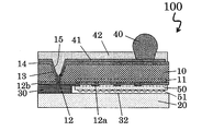
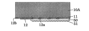
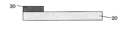
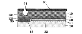
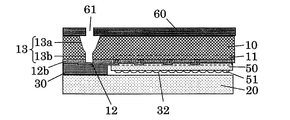
- a cavity dam 30 is formed on the transparent glass substrate 20 as a spacer surrounding the periphery of the color filter layer 50 and the microlens array 51 of the semiconductor substrate 10. Further, the cavity dam 30 of the glass substrate 20 is bonded to the first surface of the semiconductor substrate 10. That is, the transparent glass substrate 20 covers the lower side of the microlens array 51 on the first surface of the semiconductor substrate 10, and the side surface of the microlens array 51 is covered with the cavity dam 30.
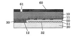
- the cavity 32 is formed in which the integrated circuit 11, the color filter layer 50, and the microlens array 51 of the semiconductor substrate 10 are closed by the glass substrate 20 and the cavity dam 30.
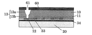
- Step 7 Bosch dry etching is performed in which etching by SF 6 and formation of a protective film on the sidewalls by C 4 F 8 (perfluorocyclobutane) are alternately performed.
- the dry etching in the Bosch mode is performed until the I / O pad 12 is reached at a coil voltage of 2500 W by alternately repeating an etching step of 6 seconds and a passivation step of 2 seconds for forming a protective film.
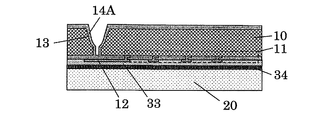
- the insulating film 14A made of SiO 2 in the vicinity of the opening of the first hole 13a of the two-stage through hole 13 had a thickness of 1.5 ⁇ m.
- An insulating film 14A having a thickness of 0.6 ⁇ m was formed on a vertical cylindrical wall surface of the second hole 13b of the through hole 13 having a two-stage structure, which is considered difficult to form a film.
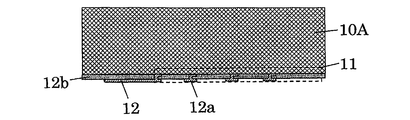
- An insulating film 14A having a thickness of 0.5 ⁇ m was formed on the I / O pad 12 at the bottom of the second hole 13b of the two-stage through hole 13.
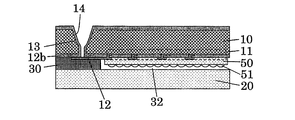
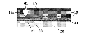
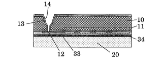
- a first hole 13 a having a wide opening portion and having a tapered hole diameter is formed on the second surface side of the semiconductor substrate 10. Since the shape is tapered, the entire first hole 13 a can be filled with the solder resist 42.
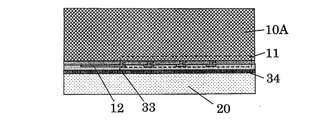
- the support substrate 12 can be bonded to the semiconductor substrate 10 using a transparent material such as quartz or glass for the support substrate 12 and using an ultraviolet curable resin for the adhesive layer 34.
- the method of peeling the semiconductor substrate 10 from the supporting substrate 12 can be peeled off by local heating of the bonding surface by laser or heating of the whole.
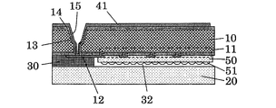
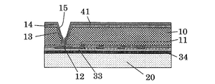
- Step 8 A copper seed layer was formed by sputtering.
- Step 9 By electrolytic plating, copper was formed thick and a conductive layer was formed to form a through electrode (TSV) 15.
- TSV through electrode
Landscapes
- Internal Circuitry In Semiconductor Integrated Circuit Devices (AREA)
- Solid State Image Pick-Up Elements (AREA)
- Drying Of Semiconductors (AREA)
- Physics & Mathematics (AREA)
- Engineering & Computer Science (AREA)
- Plasma & Fusion (AREA)
Abstract
Le dispositif à semi-conducteurs de l'invention est équipé : d'un substrat semi-conducteur qui possède une première face sur laquelle sont formés un circuit intégré ainsi qu'une plage entrée/sortie électriquement connectée au circuit intégré, et une seconde face côté opposé à la première face; d'un orifice traversant de configuration à deux niveaux qui possède une première partie forme fuselée formée sur le substrat semi-conducteur, possédant une face paroi, et dont le diamètre d'une ouverture depuis le côté seconde face jusqu'en une position prédéfinie dans la direction de l'épaisseur du substrat semi-conducteur rétrécit à l'approche d'une partie fond d'orifice, et une seconde partie forme tubulaire allant de la première partie forme à la plage entrée/sortie côté première face; d'un film isolant inorganique formé sur la seconde face et la face paroi de l'orifice traversant de configuration à deux niveaux; d'une électrode traversante d'une couche métallique formée sur la plage entrée/sortie et la face paroi de l'orifice traversant de configuration à deux niveaux; et d'un motif de câblage formé sur la seconde face, et connecté à l'électrode traversante.
Priority Applications (4)
| Application Number | Priority Date | Filing Date | Title |
|---|---|---|---|
| KR1020147018370A KR101626693B1 (ko) | 2012-01-06 | 2012-12-28 | 반도체 장치 및 그 제조 방법 |
| EP12864530.6A EP2802005B1 (fr) | 2012-01-06 | 2012-12-28 | Dispositif à semi-conducteurs, et procédé de fabrication de celui-ci |
| CN201280065944.6A CN104054164B (zh) | 2012-01-06 | 2012-12-28 | 半导体装置及其制造方法 |
| US14/321,963 US9520322B2 (en) | 2012-01-06 | 2014-07-02 | Semiconductor device and method for manufacturing same |
Applications Claiming Priority (2)
| Application Number | Priority Date | Filing Date | Title |
|---|---|---|---|
| JP2012001155A JP5810921B2 (ja) | 2012-01-06 | 2012-01-06 | 半導体装置の製造方法 |
| JP2012-001155 | 2012-01-06 |
Related Child Applications (1)
| Application Number | Title | Priority Date | Filing Date |
|---|---|---|---|
| US14/321,963 Continuation US9520322B2 (en) | 2012-01-06 | 2014-07-02 | Semiconductor device and method for manufacturing same |
Publications (1)
| Publication Number | Publication Date |
|---|---|
| WO2013103136A1 true WO2013103136A1 (fr) | 2013-07-11 |
Family
ID=48745196
Family Applications (1)
| Application Number | Title | Priority Date | Filing Date |
|---|---|---|---|
| PCT/JP2012/084110 Ceased WO2013103136A1 (fr) | 2012-01-06 | 2012-12-28 | Dispositif à semi-conducteurs, et procédé de fabrication de celui-ci |
Country Status (7)
| Country | Link |
|---|---|
| US (1) | US9520322B2 (fr) |
| EP (1) | EP2802005B1 (fr) |
| JP (1) | JP5810921B2 (fr) |
| KR (1) | KR101626693B1 (fr) |
| CN (1) | CN104054164B (fr) |
| TW (1) | TWI538132B (fr) |
| WO (1) | WO2013103136A1 (fr) |
Cited By (1)
| Publication number | Priority date | Publication date | Assignee | Title |
|---|---|---|---|---|
| WO2020022349A1 (fr) * | 2018-07-26 | 2020-01-30 | ソニー株式会社 | Élément d'imagerie à semi-conducteur, dispositif d'imagerie à semi-conducteur et procédé de fabrication d'élément d'imagerie à semi-conducteur |
Families Citing this family (19)
| Publication number | Priority date | Publication date | Assignee | Title |
|---|---|---|---|---|
| JP6185813B2 (ja) * | 2013-09-30 | 2017-08-23 | 三星ダイヤモンド工業株式会社 | イメージセンサ用ウエハ積層体の分断方法並びに分断装置 |
| MA36343B1 (fr) * | 2013-10-14 | 2016-04-29 | Nemotek Technologies | Procédé de métallisation en cuivre destiné à la fabrication d'un circuit intégré en utilisant la technologie wafer level packaging 3d |
| CN104617033B (zh) * | 2013-11-05 | 2018-09-14 | 中芯国际集成电路制造(上海)有限公司 | 晶圆级封装方法 |
| JP6191417B2 (ja) * | 2013-11-28 | 2017-09-06 | 凸版印刷株式会社 | 半導体素子アレイ基板の再生方法 |
| JP5913489B2 (ja) * | 2014-09-03 | 2016-04-27 | 三星ダイヤモンド工業株式会社 | イメージセンサ用ウエハ積層体のスクライブライン形成及び分断方法並びにスクライブライン形成及び分断装置 |
| US10622402B2 (en) | 2015-03-31 | 2020-04-14 | Hamamatsu Photonics K.K. | Semiconductor device |
| JP6725231B2 (ja) * | 2015-10-06 | 2020-07-15 | ソニーセミコンダクタソリューションズ株式会社 | 固体撮像素子、および電子装置 |
| TWI702655B (zh) * | 2016-04-13 | 2020-08-21 | 日商濱松赫德尼古斯股份有限公司 | 半導體裝置及其製造方法 |
| US10794679B2 (en) | 2016-06-29 | 2020-10-06 | Corning Incorporated | Method and system for measuring geometric parameters of through holes |
| JP6838893B2 (ja) | 2016-08-25 | 2021-03-03 | キヤノン株式会社 | 半導体装置及びその製造方法 |
| US11078112B2 (en) | 2017-05-25 | 2021-08-03 | Corning Incorporated | Silica-containing substrates with vias having an axially variable sidewall taper and methods for forming the same |
| US10580725B2 (en) * | 2017-05-25 | 2020-03-03 | Corning Incorporated | Articles having vias with geometry attributes and methods for fabricating the same |
| US12180108B2 (en) | 2017-12-19 | 2024-12-31 | Corning Incorporated | Methods for etching vias in glass-based articles employing positive charge organic molecules |
| JP2020155591A (ja) * | 2019-03-20 | 2020-09-24 | 株式会社東芝 | 半導体装置 |
| JP7340965B2 (ja) | 2019-06-13 | 2023-09-08 | キヤノン株式会社 | 半導体装置およびその製造方法 |
| US20230178579A1 (en) * | 2020-03-31 | 2023-06-08 | Sony Semiconductor Solutions Corporation | Light receiving element and electronic device |
| WO2023021670A1 (fr) * | 2021-08-19 | 2023-02-23 | オリンパス株式会社 | Dispositif à semi-conducteurs, unité d'imagerie, endoscope et procédé de fabrication de dispositifs à semi-conducteurs |
| JP7823433B2 (ja) * | 2022-03-08 | 2026-03-04 | セイコーエプソン株式会社 | 回路基板、回路基板の製造方法、及び振動デバイス |
| US20240178164A1 (en) * | 2022-11-28 | 2024-05-30 | Texas Instruments Incorporated | Sensor package with low aspect ratio through silicon via |
Citations (7)
| Publication number | Priority date | Publication date | Assignee | Title |
|---|---|---|---|---|
| JP2003503855A (ja) * | 1999-06-28 | 2003-01-28 | インテル・コーポレーション | インターポーザおよびその製造方法 |
| JP2003318178A (ja) * | 2002-04-24 | 2003-11-07 | Seiko Epson Corp | 半導体装置及びその製造方法、回路基板並びに電子機器 |
| US20060046463A1 (en) * | 2004-08-24 | 2006-03-02 | Watkins Charles M | Method of forming vias in semiconductor substrates without damaging active regions thereof and resulting structures |
| JP2007053149A (ja) | 2005-08-16 | 2007-03-01 | Renesas Technology Corp | 半導体ウエハ及びその製造方法 |
| JP2007311771A (ja) * | 2006-04-21 | 2007-11-29 | Sanyo Electric Co Ltd | 半導体装置及びその製造方法 |
| JP2008288309A (ja) * | 2007-05-16 | 2008-11-27 | Sony Corp | 半導体装置及びその製造方法 |
| JP2011003863A (ja) | 2009-06-22 | 2011-01-06 | Toshiba Corp | 半導体装置およびカメラモジュール |
Family Cites Families (12)
| Publication number | Priority date | Publication date | Assignee | Title |
|---|---|---|---|---|
| US6960837B2 (en) * | 2002-02-26 | 2005-11-01 | International Business Machines Corporation | Method of connecting core I/O pins to backside chip I/O pads |
| JP2005311117A (ja) | 2004-04-22 | 2005-11-04 | Sanyo Electric Co Ltd | 半導体装置及びその製造方法 |
| US7081408B2 (en) * | 2004-10-28 | 2006-07-25 | Intel Corporation | Method of creating a tapered via using a receding mask and resulting structure |
| JP2007305960A (ja) * | 2006-04-14 | 2007-11-22 | Sharp Corp | 半導体装置およびその製造方法 |
| JP2007295280A (ja) * | 2006-04-25 | 2007-11-08 | Toshiba Corp | 電子素子 |
| JP4937842B2 (ja) * | 2007-06-06 | 2012-05-23 | ルネサスエレクトロニクス株式会社 | 半導体装置およびその製造方法 |
| US7863721B2 (en) * | 2008-06-11 | 2011-01-04 | Stats Chippac, Ltd. | Method and apparatus for wafer level integration using tapered vias |
| JP4601686B2 (ja) * | 2008-06-17 | 2010-12-22 | ルネサスエレクトロニクス株式会社 | 半導体装置および半導体装置の製造方法 |
| US20100013060A1 (en) * | 2008-06-22 | 2010-01-21 | Taiwan Semiconductor Manufacturing Company, Ltd. | Method of forming a conductive trench in a silicon wafer and silicon wafer comprising such trench |
| US8105889B2 (en) * | 2009-07-27 | 2012-01-31 | Cree, Inc. | Methods of fabricating transistors including self-aligned gate electrodes and source/drain regions |
| CN102263192B (zh) * | 2010-05-31 | 2016-02-03 | 精材科技股份有限公司 | 发光二极管次基板、发光二极管封装及其制造方法 |
| JP2010251791A (ja) * | 2010-06-24 | 2010-11-04 | Sanyo Electric Co Ltd | 半導体装置及びその製造方法 |
-
2012
- 2012-01-06 JP JP2012001155A patent/JP5810921B2/ja not_active Expired - Fee Related
- 2012-12-28 CN CN201280065944.6A patent/CN104054164B/zh active Active
- 2012-12-28 EP EP12864530.6A patent/EP2802005B1/fr active Active
- 2012-12-28 KR KR1020147018370A patent/KR101626693B1/ko active Active
- 2012-12-28 WO PCT/JP2012/084110 patent/WO2013103136A1/fr not_active Ceased
-
2013
- 2013-01-03 TW TW102100110A patent/TWI538132B/zh active
-
2014
- 2014-07-02 US US14/321,963 patent/US9520322B2/en active Active
Patent Citations (7)
| Publication number | Priority date | Publication date | Assignee | Title |
|---|---|---|---|---|
| JP2003503855A (ja) * | 1999-06-28 | 2003-01-28 | インテル・コーポレーション | インターポーザおよびその製造方法 |
| JP2003318178A (ja) * | 2002-04-24 | 2003-11-07 | Seiko Epson Corp | 半導体装置及びその製造方法、回路基板並びに電子機器 |
| US20060046463A1 (en) * | 2004-08-24 | 2006-03-02 | Watkins Charles M | Method of forming vias in semiconductor substrates without damaging active regions thereof and resulting structures |
| JP2007053149A (ja) | 2005-08-16 | 2007-03-01 | Renesas Technology Corp | 半導体ウエハ及びその製造方法 |
| JP2007311771A (ja) * | 2006-04-21 | 2007-11-29 | Sanyo Electric Co Ltd | 半導体装置及びその製造方法 |
| JP2008288309A (ja) * | 2007-05-16 | 2008-11-27 | Sony Corp | 半導体装置及びその製造方法 |
| JP2011003863A (ja) | 2009-06-22 | 2011-01-06 | Toshiba Corp | 半導体装置およびカメラモジュール |
Non-Patent Citations (1)
| Title |
|---|
| See also references of EP2802005A4 |
Cited By (4)
| Publication number | Priority date | Publication date | Assignee | Title |
|---|---|---|---|---|
| WO2020022349A1 (fr) * | 2018-07-26 | 2020-01-30 | ソニー株式会社 | Élément d'imagerie à semi-conducteur, dispositif d'imagerie à semi-conducteur et procédé de fabrication d'élément d'imagerie à semi-conducteur |
| JPWO2020022349A1 (ja) * | 2018-07-26 | 2021-08-05 | ソニーグループ株式会社 | 固体撮像素子、固体撮像装置及び固体撮像素子の製造方法 |
| JP7423527B2 (ja) | 2018-07-26 | 2024-01-29 | ソニーグループ株式会社 | 固体撮像素子、固体撮像装置及び固体撮像素子の製造方法 |
| US12002832B2 (en) | 2018-07-26 | 2024-06-04 | Sony Corporation | Solid-state image sensor, solid-state imaging device, and method of manufacturing solid-state image sensor |
Also Published As
| Publication number | Publication date |
|---|---|
| US20140312506A1 (en) | 2014-10-23 |
| CN104054164B (zh) | 2017-06-30 |
| EP2802005B1 (fr) | 2022-07-06 |
| JP5810921B2 (ja) | 2015-11-11 |
| CN104054164A (zh) | 2014-09-17 |
| US9520322B2 (en) | 2016-12-13 |
| EP2802005A4 (fr) | 2015-12-09 |
| EP2802005A1 (fr) | 2014-11-12 |
| TWI538132B (zh) | 2016-06-11 |
| TW201340272A (zh) | 2013-10-01 |
| KR20140099316A (ko) | 2014-08-11 |
| KR101626693B1 (ko) | 2016-06-01 |
| JP2013140916A (ja) | 2013-07-18 |
Similar Documents
| Publication | Publication Date | Title |
|---|---|---|
| JP5810921B2 (ja) | 半導体装置の製造方法 | |
| CN101937894B (zh) | 具有贯通电极的半导体器件及其制造方法 | |
| US10056419B2 (en) | Chip package having chip connected to sensing device with redistribution layer in insulator layer | |
| US7180149B2 (en) | Semiconductor package with through-hole | |
| US7952170B2 (en) | System including semiconductor components having through interconnects and back side redistribution conductors | |
| US10249672B2 (en) | Image pickup apparatus, semiconductor apparatus, and image pickup unit | |
| US9230947B2 (en) | Method of forming 3D integrated microelectronic assembly with stress reducing interconnects | |
| US7981727B2 (en) | Electronic device wafer level scale packages and fabrication methods thereof | |
| TWI458071B (zh) | 晶片封裝體及其製造方法 | |
| US20090309176A1 (en) | Methods for protecting imaging elements of photoimagers during back side processing, photoimagers and systems | |
| US20160190353A1 (en) | Photosensitive module and method for forming the same | |
| US9966400B2 (en) | Photosensitive module and method for forming the same | |
| JP2020077855A (ja) | チップパッケージおよびその製造方法 | |
| JP2012015470A (ja) | 撮像装置および撮像装置の製造方法 | |
| US20090050995A1 (en) | Electronic device wafer level scale packges and fabrication methods thereof | |
| TWI525805B (zh) | 低輪廓影像感測器 | |
| US20120061787A1 (en) | Liquid electrical interconnect and devices using same | |
| JP2016001759A (ja) | 半導体装置 | |
| US9978788B2 (en) | Photosensitive module and method for forming the same | |
| CN114846610A (zh) | 半导体装置和半导体装置的制造方法 | |
| US20240145445A1 (en) | Semiconductor device, method for manufacturing semiconductor device, and electronic device | |
| JP2005072489A (ja) | 半導体装置の製造方法および半導体装置 | |
| CN104051489B (zh) | 小轮廓图像传感器 |
Legal Events
| Date | Code | Title | Description |
|---|---|---|---|
| 121 | Ep: the epo has been informed by wipo that ep was designated in this application |
Ref document number: 12864530 Country of ref document: EP Kind code of ref document: A1 |
|
| ENP | Entry into the national phase |
Ref document number: 20147018370 Country of ref document: KR Kind code of ref document: A |
|
| WWE | Wipo information: entry into national phase |
Ref document number: 2012864530 Country of ref document: EP |
|
| NENP | Non-entry into the national phase |
Ref country code: DE |