WO2013114592A1 - Élément de conversion thermoélectrique, et procédé de fabrication de celui-ci - Google Patents
Élément de conversion thermoélectrique, et procédé de fabrication de celui-ci Download PDFInfo
- Publication number
- WO2013114592A1 WO2013114592A1 PCT/JP2012/052283 JP2012052283W WO2013114592A1 WO 2013114592 A1 WO2013114592 A1 WO 2013114592A1 JP 2012052283 W JP2012052283 W JP 2012052283W WO 2013114592 A1 WO2013114592 A1 WO 2013114592A1
- Authority
- WO
- WIPO (PCT)
- Prior art keywords
- thin film
- region
- heating
- thermoelectric conversion
- conversion element
- Prior art date
- Legal status (The legal status is an assumption and is not a legal conclusion. Google has not performed a legal analysis and makes no representation as to the accuracy of the status listed.)
- Ceased
Links
Images




Classifications
-
- H—ELECTRICITY
- H10—SEMICONDUCTOR DEVICES; ELECTRIC SOLID-STATE DEVICES NOT OTHERWISE PROVIDED FOR
- H10N—ELECTRIC SOLID-STATE DEVICES NOT OTHERWISE PROVIDED FOR
- H10N10/00—Thermoelectric devices comprising a junction of dissimilar materials, i.e. devices exhibiting Seebeck or Peltier effects
- H10N10/80—Constructional details
- H10N10/85—Thermoelectric active materials
- H10N10/851—Thermoelectric active materials comprising inorganic compositions
- H10N10/854—Thermoelectric active materials comprising inorganic compositions comprising only metals
-
- C—CHEMISTRY; METALLURGY
- C04—CEMENTS; CONCRETE; ARTIFICIAL STONE; CERAMICS; REFRACTORIES
- C04B—LIME, MAGNESIA; SLAG; CEMENTS; COMPOSITIONS THEREOF, e.g. MORTARS, CONCRETE OR LIKE BUILDING MATERIALS; ARTIFICIAL STONE; CERAMICS; REFRACTORIES; TREATMENT OF NATURAL STONE
- C04B35/00—Shaped ceramic products characterised by their composition; Ceramics compositions; Processing powders of inorganic compounds preparatory to the manufacturing of ceramic products
- C04B35/01—Shaped ceramic products characterised by their composition; Ceramics compositions; Processing powders of inorganic compounds preparatory to the manufacturing of ceramic products based on oxide ceramics
- C04B35/46—Shaped ceramic products characterised by their composition; Ceramics compositions; Processing powders of inorganic compounds preparatory to the manufacturing of ceramic products based on oxide ceramics based on titanium oxides or titanates
- C04B35/462—Shaped ceramic products characterised by their composition; Ceramics compositions; Processing powders of inorganic compounds preparatory to the manufacturing of ceramic products based on oxide ceramics based on titanium oxides or titanates based on titanates
- C04B35/465—Shaped ceramic products characterised by their composition; Ceramics compositions; Processing powders of inorganic compounds preparatory to the manufacturing of ceramic products based on oxide ceramics based on titanium oxides or titanates based on titanates based on alkaline earth metal titanates
- C04B35/47—Shaped ceramic products characterised by their composition; Ceramics compositions; Processing powders of inorganic compounds preparatory to the manufacturing of ceramic products based on oxide ceramics based on titanium oxides or titanates based on titanates based on alkaline earth metal titanates based on strontium titanates
-
- C—CHEMISTRY; METALLURGY
- C23—COATING METALLIC MATERIAL; COATING MATERIAL WITH METALLIC MATERIAL; CHEMICAL SURFACE TREATMENT; DIFFUSION TREATMENT OF METALLIC MATERIAL; COATING BY VACUUM EVAPORATION, BY SPUTTERING, BY ION IMPLANTATION OR BY CHEMICAL VAPOUR DEPOSITION, IN GENERAL; INHIBITING CORROSION OF METALLIC MATERIAL OR INCRUSTATION IN GENERAL
- C23C—COATING METALLIC MATERIAL; COATING MATERIAL WITH METALLIC MATERIAL; SURFACE TREATMENT OF METALLIC MATERIAL BY DIFFUSION INTO THE SURFACE, BY CHEMICAL CONVERSION OR SUBSTITUTION; COATING BY VACUUM EVAPORATION, BY SPUTTERING, BY ION IMPLANTATION OR BY CHEMICAL VAPOUR DEPOSITION, IN GENERAL
- C23C14/00—Coating by vacuum evaporation, by sputtering or by ion implantation of the coating forming material
- C23C14/06—Coating by vacuum evaporation, by sputtering or by ion implantation of the coating forming material characterised by the coating material
- C23C14/08—Oxides
- C23C14/088—Oxides of the type ABO3 with A representing alkali, alkaline earth metal or Pb and B representing a refractory or rare earth metal
-
- H—ELECTRICITY
- H10—SEMICONDUCTOR DEVICES; ELECTRIC SOLID-STATE DEVICES NOT OTHERWISE PROVIDED FOR
- H10N—ELECTRIC SOLID-STATE DEVICES NOT OTHERWISE PROVIDED FOR
- H10N10/00—Thermoelectric devices comprising a junction of dissimilar materials, i.e. devices exhibiting Seebeck or Peltier effects
- H10N10/01—Manufacture or treatment
-
- H—ELECTRICITY
- H10—SEMICONDUCTOR DEVICES; ELECTRIC SOLID-STATE DEVICES NOT OTHERWISE PROVIDED FOR
- H10N—ELECTRIC SOLID-STATE DEVICES NOT OTHERWISE PROVIDED FOR
- H10N10/00—Thermoelectric devices comprising a junction of dissimilar materials, i.e. devices exhibiting Seebeck or Peltier effects
- H10N10/10—Thermoelectric devices comprising a junction of dissimilar materials, i.e. devices exhibiting Seebeck or Peltier effects operating with only the Peltier or Seebeck effects
- H10N10/17—Thermoelectric devices comprising a junction of dissimilar materials, i.e. devices exhibiting Seebeck or Peltier effects operating with only the Peltier or Seebeck effects characterised by the structure or configuration of the cell or thermocouple forming the device
-
- H—ELECTRICITY
- H10—SEMICONDUCTOR DEVICES; ELECTRIC SOLID-STATE DEVICES NOT OTHERWISE PROVIDED FOR
- H10N—ELECTRIC SOLID-STATE DEVICES NOT OTHERWISE PROVIDED FOR
- H10N10/00—Thermoelectric devices comprising a junction of dissimilar materials, i.e. devices exhibiting Seebeck or Peltier effects
- H10N10/80—Constructional details
- H10N10/85—Thermoelectric active materials
- H10N10/851—Thermoelectric active materials comprising inorganic compositions
- H10N10/855—Thermoelectric active materials comprising inorganic compositions comprising compounds containing boron, carbon, oxygen or nitrogen
-
- C—CHEMISTRY; METALLURGY
- C04—CEMENTS; CONCRETE; ARTIFICIAL STONE; CERAMICS; REFRACTORIES
- C04B—LIME, MAGNESIA; SLAG; CEMENTS; COMPOSITIONS THEREOF, e.g. MORTARS, CONCRETE OR LIKE BUILDING MATERIALS; ARTIFICIAL STONE; CERAMICS; REFRACTORIES; TREATMENT OF NATURAL STONE
- C04B2235/00—Aspects relating to ceramic starting mixtures or sintered ceramic products
- C04B2235/02—Composition of constituents of the starting material or of secondary phases of the final product
- C04B2235/30—Constituents and secondary phases not being of a fibrous nature
- C04B2235/32—Metal oxides, mixed metal oxides, or oxide-forming salts thereof, e.g. carbonates, nitrates, (oxy)hydroxides, chlorides
- C04B2235/3224—Rare earth oxide or oxide forming salts thereof, e.g. scandium oxide
- C04B2235/3227—Lanthanum oxide or oxide-forming salts thereof
-
- C—CHEMISTRY; METALLURGY
- C04—CEMENTS; CONCRETE; ARTIFICIAL STONE; CERAMICS; REFRACTORIES
- C04B—LIME, MAGNESIA; SLAG; CEMENTS; COMPOSITIONS THEREOF, e.g. MORTARS, CONCRETE OR LIKE BUILDING MATERIALS; ARTIFICIAL STONE; CERAMICS; REFRACTORIES; TREATMENT OF NATURAL STONE
- C04B2235/00—Aspects relating to ceramic starting mixtures or sintered ceramic products
- C04B2235/02—Composition of constituents of the starting material or of secondary phases of the final product
- C04B2235/30—Constituents and secondary phases not being of a fibrous nature
- C04B2235/32—Metal oxides, mixed metal oxides, or oxide-forming salts thereof, e.g. carbonates, nitrates, (oxy)hydroxides, chlorides
- C04B2235/3231—Refractory metal oxides, their mixed metal oxides, or oxide-forming salts thereof
- C04B2235/3251—Niobium oxides, niobates, tantalum oxides, tantalates, or oxide-forming salts thereof
-
- C—CHEMISTRY; METALLURGY
- C04—CEMENTS; CONCRETE; ARTIFICIAL STONE; CERAMICS; REFRACTORIES
- C04B—LIME, MAGNESIA; SLAG; CEMENTS; COMPOSITIONS THEREOF, e.g. MORTARS, CONCRETE OR LIKE BUILDING MATERIALS; ARTIFICIAL STONE; CERAMICS; REFRACTORIES; TREATMENT OF NATURAL STONE
- C04B2235/00—Aspects relating to ceramic starting mixtures or sintered ceramic products
- C04B2235/70—Aspects relating to sintered or melt-casted ceramic products
- C04B2235/74—Physical characteristics
- C04B2235/76—Crystal structural characteristics, e.g. symmetry
- C04B2235/768—Perovskite structure ABO3
-
- C—CHEMISTRY; METALLURGY
- C04—CEMENTS; CONCRETE; ARTIFICIAL STONE; CERAMICS; REFRACTORIES
- C04B—LIME, MAGNESIA; SLAG; CEMENTS; COMPOSITIONS THEREOF, e.g. MORTARS, CONCRETE OR LIKE BUILDING MATERIALS; ARTIFICIAL STONE; CERAMICS; REFRACTORIES; TREATMENT OF NATURAL STONE
- C04B2235/00—Aspects relating to ceramic starting mixtures or sintered ceramic products
- C04B2235/70—Aspects relating to sintered or melt-casted ceramic products
- C04B2235/74—Physical characteristics
- C04B2235/78—Grain sizes and shapes, product microstructures, e.g. acicular grains, equiaxed grains, platelet-structures
-
- C—CHEMISTRY; METALLURGY
- C04—CEMENTS; CONCRETE; ARTIFICIAL STONE; CERAMICS; REFRACTORIES
- C04B—LIME, MAGNESIA; SLAG; CEMENTS; COMPOSITIONS THEREOF, e.g. MORTARS, CONCRETE OR LIKE BUILDING MATERIALS; ARTIFICIAL STONE; CERAMICS; REFRACTORIES; TREATMENT OF NATURAL STONE
- C04B2235/00—Aspects relating to ceramic starting mixtures or sintered ceramic products
- C04B2235/70—Aspects relating to sintered or melt-casted ceramic products
- C04B2235/74—Physical characteristics
- C04B2235/78—Grain sizes and shapes, product microstructures, e.g. acicular grains, equiaxed grains, platelet-structures
- C04B2235/787—Oriented grains
Definitions
- Embodiment described below is related with a thermoelectric conversion element and its manufacturing method.
- thermoelectric conversion element using the Seebeck effect does not require a working fluid or a complicated drive mechanism like the conventional thermoelectric conversion system, and can recover waste heat from various systems and convert it into electric power.
- the power factor PF reaches a value of 35 ⁇ W / cmK 2 to 40 ⁇ W / cmK 2 , but the thermal conductivity ⁇ has a large value of 11 W / mK in the case of a bulk crystal.
- T is the absolute temperature
- S is the Seebeck coefficient of STO
- ⁇ is the resistivity of STO
- ⁇ is the thermal conductivity of STO.
- thermoelectric conversion element made of STO In order to obtain a large figure of merit ZT in such a thermoelectric conversion element made of STO, it is necessary to give the STO high conductivity and at the same time reduce its thermal conductivity ⁇ .
- JP 2010-161213 A Cahill, D. Rev. Sci. Instrum. 61 (2), February 1990, pp802-808 Cahill, D., et al. Phys. Rev. B Vol. 50, Number 9, 6077-6081 (1994) Ravichandran, J., et al., Phys. Rev. B 82, 165126 (2010)
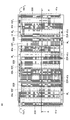
- the thermoelectric conversion element includes a substrate, a thin film formed on the substrate and made of a compound having a perovskite structure, and provided on the substrate, in contact with the upper surface of the thin film in a first region.
- One electrode a second electrode that contacts the upper surface of the thin film in a second region spaced from the first region, and a first heating or cooling device that heats or cools the thin film in the first region.
- a cooling unit and a second heating or cooling unit that heats or cools the thin film in the second region.
- the second heating or cooling unit includes the first heating or cooling unit.
- the first region of the thin film is cooled, and the second heating or cooling unit is the first heating or cooling unit of the first region of the thin film.
- the second region of the thin film is heated to, for the thin film, in the crystal constituting the compound of the perovskite structure, are regions of different crystal orientation formed with the crystal.
- thermoelectric conversion element since a plurality of domains having a crystal orientation different from that of the matrix are formed in the perovskite thin film, phonon scattering is induced by the dislocation of the domain boundary. As a result, the thermal conductivity of the perovskite thin film is reduced, and the figure of merit ZT of the thermoelectric conversion element is improved.
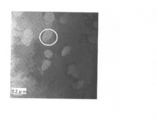
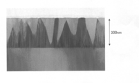
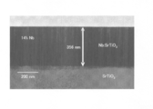
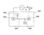
- Sectional drawing which shows the STO thin film doped with La and Nb used as the thermoelectric conversion element by 1st Embodiment. It is a flowchart which shows the manufacturing process of the STO thin film by 1st Embodiment. It is a graph showing the relationship between electrical conductivity and total dope amount about the STO thin film of FIG. 3 is a transmission electron microscope image of the STO thin film of FIG. 2 viewed from a direction perpendicular to the film surface. It is a transmission electron microscope image which shows the film
- FIG. 7 It is a figure explaining the measurement of the thermal conductivity by 3omega method. It is a graph explaining the measurement of the heat conductivity by 3omega method. It is a figure explaining the experiment which confirms the uniformity of the STO thin film of FIG.
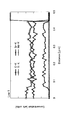
- FIG. 7 it is a figure which shows the composition profile along line Line1.
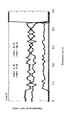
- FIG. 7 it is a figure which shows the composition profile along line Line2.
- FIG. 7 it is a figure which overlaps and shows the profile of Drawing 8A and Drawing 8B.
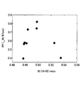
- 3 is a graph showing the relationship between oxygen heat treatment and carrier concentration of the STO thin film of FIG. It is a graph which shows the power factor of the thermoelectric conversion element of FIG. It is sectional drawing which shows the structure of the thermoelectric conversion element by 1st Embodiment. It is a top view which shows the structure of the thermoelectric conversion element by 2nd Embodiment.
- FIG. 12B is a cross-sectional view taken along line AA ′ in FIG. 12A.
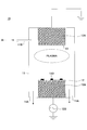
- FIG. 1 is a diagram showing a configuration of a sputtering apparatus 10 used for forming an STO thin film in the first embodiment. Note that the formation of the STO thin film in the present embodiment is not limited to the sputtering method using the sputtering apparatus 10 of FIG. 1, but can be formed by other PVD methods, for example, a pulse laser deposition method.
- a sputtering apparatus 10 includes a vacuum vessel 11 into which a sputtering gas such as Ar is introduced from a sputtering gas introduction port 11B and is evacuated to a high vacuum at an exhaust port 11A.
- a target holding base 12A for holding a target 12 made of STO is provided.
- a substrate holder 13A for holding the substrate to be processed 13 is provided above the vacuum container 11 so that the substrate to be processed 13 faces the target 12.
- a high frequency power source 12B is connected to the target holding base 12A, and the high frequency power source 12B applies the high frequency to the target 12 via the target holding base 12A.
- Plasma is generated between the processing substrate 13 and the generated plasma collides with the target 12, whereby the components of the target 12 are sputtered from the target 12.
- the substrate holder 13A is grounded, and the components sputtered from the target 12 are deposited on the substrate 13 to be processed on the substrate holder 13A, and a desired STO thin film is formed on the substrate 13 to be processed.
- the metal pieces 12D of the metal element to be doped into the strontium titanate thin film are arranged on the target 12 at a predetermined ratio.
- the thin film can be doped with a desired metal element at a desired ratio.
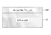
- FIG. 2 is a schematic sectional view showing an STO thin film 23F used as a thermoelectric conversion element according to the first embodiment
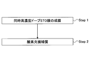
- FIG. 3 is a flowchart showing a manufacturing process of the STO thin film 23F in FIG.
- the STO thin film 23F is a film having a non-stoichiometric composition or a stoichiometric composition having oxygen deficiency, and has a film thickness in the range of 1 nm to 10 ⁇ m, preferably in the range of 10 nm to 1000 nm.
- the A seat is doped with Sr and the B seat is simultaneously doped with Nb at a high concentration, and the composition represented by the general formula (Sr, La) (Nb, Ti) 1 ⁇ ⁇ O 3 is obtained.
- the general formula (Sr, La) (Nb, Ti) 1 ⁇ ⁇ O 3 is obtained.
- the A and B seats of the STO thin film 23F are the ratio of the total number of atoms of Sr and Nb to the total of the A and B seats expressed by (La + Nb) / (Sr + La + Ti + Nb), and therefore the atomic concentration is 20% or more.
- Step 1 the sputtering apparatus 10 of FIG. 1 is formed on a suitable substrate, for example, a single crystal substrate 13 of strontium titanate or lanthanum aluminate (LaAlO 3 ). Is used to epitaxially form the STO thin film 23F highly doped with La and Nb.
- a suitable substrate for example, a single crystal substrate 13 of strontium titanate or lanthanum aluminate (LaAlO 3 ).
- the STO thin film 23F obtained in this way is heat-treated in an oxygen atmosphere in Step 2 to control the oxygen deficiency concentration in the STO thin film 23F.
- the carrier concentration in the film increases, the resistivity ⁇ in the equation (1) is reduced, and the electrical conductivity ⁇ is increased. Can do.
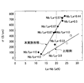
- FIG. 4 shows the hole mobility of electrons and the atoms occupying the B seat in the STO thin film 23F doped with La and Nb thus formed on the STO single crystal substrate 13 with a film thickness of 300 nm.
- the relationship with the atomic ratio (B / (A + B)) for the entire A seat and B seat is shown.
- the vertical axis represents the hole mobility of electrons
- the horizontal axis represents the atomic ratio of atoms occupying the B seat to the entire A seat and B seat (B / (A + B)), and accordingly ((La + Nb) / (Sr + La + Ti + Nb)).
- the atomic ratio is shown.
- the numerical value given to each point in FIG. 3 indicates the atomic ratio Nb / La between Nb and La.
- the electrical conductivity ⁇ of the STO thin film 23F increases as the total atomic concentration of Nb and La defined above increases, which is caused by doping. This reflects the situation where the carrier concentration in the thin film is increasing. In particular, when the total atomic concentration is increased beyond 20%, the electrical conductivity ⁇ of the STO thin film 23F exceeds 700 S / cm and approaches 800 S / cm.
- FIG. 4 shows a comparative example in which the STO thin film 23F is not doped with La but is doped only with Nb. In this case, the electrical conductivity ⁇ of the STO thin film is reduced to less than half.
- 5A and 5B show transmission electron micrographs of the thin film obtained when the STO thin film 23F of FIG. 2 is doped with La and Ni at a concentration exceeding 20 atomic% at the same time. It is a figure shown about a film cross section.
- the STO film 23F doped in such a high concentration is a single crystal film, but is shown in white in a (001) plane orientation matrix shown in black in the film. It can be seen that many (031) plane orientation regions or domains are generated. As can be seen from FIG. 5A, the size of the generated domain of the (031) plane orientation is 0.2 ⁇ m, and it is considered that dislocations are formed at the boundary with the matrix.
- FIGS. 5A and 5B actually use a LaAlO 3 (LAO) substrate as the substrate 13 as described later in Example 1, and the STO thin film 23F has a concentration of 13.02 atomic% with La. Further, Nb is co-doped at a concentration of 8.4 atomic%, and RF magnetron sputtering is performed at a substrate temperature of 700 ° C. in a 1 Pa Ar gas atmosphere in the sputtering apparatus 10 of FIG. It was obtained by executing while supplying.
- LAO LaAlO 3
- the STO film 23F having a structure including such a domain it is considered that phonon scattering occurs due to dislocations existing at the domain boundary, and the thermal conductivity ⁇ in the film is greatly reduced. Therefore, there is a possibility that the figure of merit ZT can be greatly improved by using such an STO thin film 23F for a thermoelectric conversion element.
- FIG. 5C shows a comparative example, in which the STO thin film 23F of FIG. 2 is doped with Nb to a concentration of 14 atomic%, but in this case, no remarkable domain structure is observed.
- the domain structure of FIGS. 5A and 5B appears when the total dopant concentration exceeds 20%. ing.
- a similar domain structure appears when the dopant concentration exceeds 25%.
- the carrier concentration in the film is lowered as described above, but such a domain structure can be formed, and such a case is also included in this embodiment.
- 5A and 5B are prepared by arranging nine La pieces and Nb pieces as the metal pieces 12D on the target 12 in the sputtering apparatus 10 of FIG. 1, and the Nb in the thin film 23F is produced.
- the concentration is confirmed by inductively coupled plasma (ICP) spectroscopy.
- 5C is produced by arranging three Nb pieces as the metal piece 12D on the target 12 in the sputtering apparatus 10 shown in FIG. 1.
- the Nb concentration in the thin film 23F is determined by inductively coupled plasma. (ICP) Confirmed by spectroscopy.
- the thermal conductivity was measured by the 3 ⁇ method for the structure in which such a domain occurs.
- Non-patent documents 1 and 2 explain the principle and application examples of the 3 ⁇ method.
- FIG. 6A is a diagram showing an outline of measurement
- FIG. 6B is a graph showing measurement data.
- a thin silicon oxide film (not shown) is formed on the STO thin film 23F of FIG. 2 by sputtering for insulation, and a Cr / Au laminated structure is formed thereon. Measurement was performed by forming a line-shaped heater 23H from a conductive film, supplying alternating current having a frequency ⁇ from both terminals 23A and 23B to the heater 23H, and periodically heating the heater 23H.
- the heater 23H is also used as a temperature measuring device. Such temperature oscillation ⁇ T is caused by the diffusion of heat from the heater 23H that is periodically heated along the sample surface, and includes information on the thermal conductivity ⁇ of the sample.
- lines L 1R and L 1I show the relationship between the temperature oscillation ⁇ T and the logarithm of the heating frequency ⁇ thus obtained for the sample of FIG.
- the line L 1R represents the real part of the temperature oscillation ⁇ T that is in phase with the heating cycle, and forms a straight line with respect to the logarithm of the heating frequency ⁇ .
- the line L 1I represents the imaginary part of the temperature oscillation ⁇ T that is in opposite phase to the heating cycle, and is constant with respect to the heating frequency ⁇ .
- lines RL 1R and RL 1I are obtained when the electrode of FIG. 6A is formed directly on the STO substrate 13 without forming the STO thin film 23F in the sample of FIG. It is a line which shows the relationship between the temperature vibration (DELTA) T of the said STO board
- the line RL 1R represents the real part of the temperature oscillation ⁇ T that is in phase with the heating cycle and is linear with the logarithm of the heating frequency ⁇ .
- the line RL 1I represents the imaginary part of the temperature oscillation ⁇ T that is in opposite phase to the heating cycle, and is constant with respect to the heating frequency ⁇ .
- the thermal conductivity ⁇ of the STO substrate 13 (Sub) is calculated as 11.2 W / mK based on the slope of the line RL 1R , which is known as the thermal conductivity of the STO bulk single crystal. Matches the value of.
- the line L 1R is parallel to the line RL 1R and is shifted upward by about 0.7K.
- This shift amount ⁇ T film corresponds to the contribution of the thermal conductivity ⁇ of the STO thin film 23F.
- this shift amount ⁇ T film is independent of the heating frequency ⁇ , this corresponds to the situation in which the diffusion of heat in the surface direction of the sample can be ignored because the thin film 23F is thin.
- the STO thin film 23F according to the present embodiment includes the domain structure described above with reference to FIGS. 5A and 5B, phonon scattering is promoted in the film, and the thermal conductivity ⁇ is conventional, that is, non-patent literature. This is considered to be further reduced as compared with the STO thin film No. 3.
- Example 1 an LAO substrate is used as the substrate 13, and an (001) -oriented STO thin film 23F on which La and Nb are simultaneously doped is formed by the sputtering apparatus 10 of FIG.
- the substrate is formed at a substrate temperature of 700 ° C. by RF sputtering while supplying high-frequency power of 75 W under a reduced-pressure Ar atmosphere.
- the STO thin film 23F is doped with 13.2 atomic% La, 8.4 atomic% Nb, and oxygen vacancies at a rate of 16.2% per unit cell without performing heat treatment after film formation. .
- FIG. 8B is a transmission electron microscope image of the film 23F viewed from the direction perpendicular to the film surface
- FIG. 8A is a composition profile along the straight line 1 in FIG. 7
- FIG. 8B is a composition along the straight line 2 in FIG.
- FIG. 8C is a view obtained by superimposing FIG. 8A and FIG. 8B.
- the straight line 1 and the straight line 2 are about 0.2 ⁇ m apart as shown in FIG.
- Example 2 the sample of Example 1 was further heat-treated in an oxygen atmosphere to optimize the power factor PF.
- FIG. 9 is a graph showing the relationship between the electron concentration n H obtained by the Hall effect in the STO thin film 23F according to Example 2 and the heat treatment temperature.
- the vertical axis indicates the electron concentration n H and the horizontal axis indicates the heat treatment temperature.
- the heat treatment is performed in an oxygen atmosphere of 1 atm for 2 hours.
- the electron concentration n H in the film is 10 20 cm ⁇ 3 to 10 ⁇ 10. It can be seen that it is possible to adjust to a range of 22 cm ⁇ 3 .
- the power factor PF S 2 qn ⁇ increases as described at the beginning.
- FIG. 9 shows that heat treatment in an oxygen atmosphere at a relatively low temperature of 20 ° C. to 600 ° C. effectively compensates for oxygen vacancies that trap and cancel carriers in the STO thin film 23F. Yes.
- FIG. 10 is a graph showing the power factor PF when a thermoelectric conversion element described later is manufactured using the STO thin film 23F of this example.
- the vertical axis represents the power factor PF
- the horizontal axis represents the ratio of the B seat element to the total (A + B) of the A seat and B seat of the perovskite structure, that is, B / (A + B).
- the power factor PF is maximized by selecting the ratio B / (A + B) in the vicinity of 0.50 in the STO film 23F having the electron concentration n H optimized as described above. I understand. This is because the total number of atoms of Sr and La occupying the A seat and the total number of Ti and Nb occupying the B seat are balanced, and the trapping or canceling of carriers by vacancies in the A seat or B seat is minimized. This corresponds to the situation where the concentration of carriers emitted by doping La, Nb, that is, electrons, is maximized.
- thermoelectric conversion element 20 Refer to FIG. 1
- the thermoelectric conversion element 20 includes the single crystal STO substrate 13, the STO thin film 23F epitaxially formed on the STO substrate 13, and first and second end portions on the STO thin film 23F.
- the first electrodes 22A and 22B made of an oxidation-resistant metal such as Pt and having a thickness of 100 nm, for example, and between the first end and the second end on the STO thin film 23F And the second electrode 24 formed in the region.
- thermoelectric conversion element 20 of FIG. 11 for example, the bottom surface of the substrate 13 is heated in a region near the first end and the second end, and the STO thin film 23F is cooled in the intermediate region. Or by cooling the bottom surface of the substrate 13 in the regions near the first end and the second end and heating the STO thin film 23F in the intermediate region, An output voltage due to the Seebeck effect is obtained between the output terminal OUT1 connected to 22B and the output terminal OUT2 connected to the second electrode 24.
- thermoelectric conversion element 20 of FIG. 11 a single crystal MgO substrate or a LaAlO 3 substrate can be used instead of the single crystal STO substrate 13.
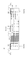
- FIG. 12A and 12B are a cross-sectional view and a plan view showing the configuration of the thermoelectric conversion device 40 according to the second embodiment, respectively.
- FIG. 12A shows a cross section along line AA ′ in the plan view of FIG. 12B.
- the thermoelectric conversion device 40 includes the single crystal STO substrate 13 and an STO thin film pattern formed on the substrate 13 and having the same structure as the STO thin film 23F of FIGS. 5A and 5B.
- 23F 1 , 23F 2 , 23F 3 , 23F 4 the STO thin film pattern 23F 1 has electrodes 22A and 22B at both ends thereof and electrodes 24 at the intermediate portion thereof. The same applies to the other STO thin film patterns 23F 2 , 23F 3 , and 23F 4 .
- STO thin film pattern - STO thin film pattern electrodes 22A and 22B on the emission 23F 1 adjacent connected in parallel - a first wiring W 1 to be connected to the electrode 24 on the emission 23F 2 is also the STO thin film pattern - STO thin film pattern electrodes 22A and 22B on the emission 23F 2 adjacent connected in parallel - a second wiring connected to the electrode 24 on the emission 23F 3 W 2 further wherein STO thin film pattern - down 23F STO thin film pattern electrodes 22A and 22B on 2 adjacent connected in parallel - the third wire W 3 to be connected to the electrode 24 on the emission 23F 3, further wherein the STO thin film pattern - electrode 22A on the emission 23F 4 and fourth wire W 4 which are connected in parallel 22B are formed.
- a heating / cooling device 41 having protrusions 41A, 41B, 41C, and 41D is shown with the protrusions 41A, 41B, 41C, and 41D surrounded by broken lines in FIG. 12A, respectively.
- the region 41a corresponds to the electrode 22A formed on the STO thin film 23f1
- the region 41b is the STO thin film 23F 1 electrode 22B formed on and the STO thin film 23F electrode 22A formed on the 2 corresponds to the region 41c corresponds to the STO thin film 23F 2 electrode 22B formed on and the STO thin film 23F 3 electrodes 22A formed on the area 41d is the STO thin film 23F 3 correspond to the formed electrode 22B and the STO thin film 23F 4 electrodes 22A formed on the upper
- the region 41e corresponds to the electrode 22B formed on the STO thin film 23F 4.
- a heating / cooling device 42 having projecting portions 42A, 42B, 42C, and 42D, and the projecting portions 42A, 42B, 42C, and 42D are shown by broken lines in FIG. 12A.
- the STO thin film 23F 1 area 42a enclosed by a also in the region 42b of the STO thin film 23F 2, also in the area 41c of the STO thin film 23F 3, also in the region 41d of the STO thin film 23F 4, provided in contact respectively
- the STO thin films 23F 1 to 23F 4 are cooled or heated in the regions 42a to 42e.
- the region 42a corresponds to the electrode 24 formed on the STO thin film 23F 1, wherein the region 41b corresponds to electrode 24 formed on the STO thin film 23F 2, the region 41c is the STO correspond to the electrodes 24 formed on the thin film 23F3, the area 41d corresponds to electrode 24 formed on the STO thin film 23F 4.
- the heating and cooling device 42 a central portion of the STO thin film 23F 1 ⁇ 23F 4 is cooled when the heating and cooling apparatus 4 1 heats the both end portions of the STO thin film 23F 1 ⁇ 23F 4 through the substrate 13
- the heating / cooling device 41 cools both ends of the STO thin films 23F1 to 23F4 via the substrate 13
- the central portions of the STO thin films 23F 1 to 23F 4 are heated, and the respective STO thin films 23F 1 to 23F 1 to in 23F 4 induces a temperature gradient in the lateral direction.
- thermoelectric conversion element is formed by the STO thin film that swings the domain structure.
- the thermoelectric conversion element using another perovskite film for example, a BaTiO 3 film
- the high concentration doping is performed.
- a similar domain structure can be generated in the perovskite film, and the thermal conductivity ⁇ can be reduced.
Landscapes
- Chemical & Material Sciences (AREA)
- Engineering & Computer Science (AREA)
- Organic Chemistry (AREA)
- Ceramic Engineering (AREA)
- Materials Engineering (AREA)
- Manufacturing & Machinery (AREA)
- Inorganic Chemistry (AREA)
- Structural Engineering (AREA)
- Chemical Kinetics & Catalysis (AREA)
- Mechanical Engineering (AREA)
- Metallurgy (AREA)
- Physical Vapour Deposition (AREA)
- Physical Deposition Of Substances That Are Components Of Semiconductor Devices (AREA)
- Compositions Of Oxide Ceramics (AREA)
- Inorganic Compounds Of Heavy Metals (AREA)
Abstract
L'élément de conversion thermoélectrique de l'invention contient : un substrat; un film mince formé sur ledit substrat, et constitué d'un composé de structure pérovskite; une première électrode agencée sur ledit substrat, et en contact avec une première région sur la face supérieure dudit film mince; une seconde électrode en contact avec une seconde région éloignée de ladite première région sur la face supérieure dudit film mince; une première partie chauffage ou refroidissement chauffant ou refroidissant ledit film mince dans ladite première région; et une seconde partie chauffage ou refroidissement chauffant ou refroidissant ledit film mince dans ladite seconde région. Ladite seconde partie chauffage ou refroidissement refroidit ladite première région dudit film mince lorsque ladite première partie chauffage ou refroidissement chauffe ladite seconde région dudit film mince. Ladite seconde partie chauffage ou refroidissement chauffe ladite seconde région dudit film mince lorsque ladite première partie chauffage ou refroidissement refroidit ladite première région dudit film mince. Ledit film mince présente dans des cristaux configurant ledit composé de structure pérovskite, la formation d'une région d'orientation cristalline différente desdits cristaux.
Priority Applications (3)
| Application Number | Priority Date | Filing Date | Title |
|---|---|---|---|
| JP2013556145A JP6086071B2 (ja) | 2012-02-01 | 2012-02-01 | 熱電変換素子およびその製造方法 |
| PCT/JP2012/052283 WO2013114592A1 (fr) | 2012-02-01 | 2012-02-01 | Élément de conversion thermoélectrique, et procédé de fabrication de celui-ci |
| US14/449,260 US9508912B2 (en) | 2012-02-01 | 2014-08-01 | Thermoelectric conversion device having perovskite crystal including grain domain |
Applications Claiming Priority (1)
| Application Number | Priority Date | Filing Date | Title |
|---|---|---|---|
| PCT/JP2012/052283 WO2013114592A1 (fr) | 2012-02-01 | 2012-02-01 | Élément de conversion thermoélectrique, et procédé de fabrication de celui-ci |
Related Child Applications (1)
| Application Number | Title | Priority Date | Filing Date |
|---|---|---|---|
| US14/449,260 Continuation US9508912B2 (en) | 2012-02-01 | 2014-08-01 | Thermoelectric conversion device having perovskite crystal including grain domain |
Publications (1)
| Publication Number | Publication Date |
|---|---|
| WO2013114592A1 true WO2013114592A1 (fr) | 2013-08-08 |
Family
ID=48904670
Family Applications (1)
| Application Number | Title | Priority Date | Filing Date |
|---|---|---|---|
| PCT/JP2012/052283 Ceased WO2013114592A1 (fr) | 2012-02-01 | 2012-02-01 | Élément de conversion thermoélectrique, et procédé de fabrication de celui-ci |
Country Status (3)
| Country | Link |
|---|---|
| US (1) | US9508912B2 (fr) |
| JP (1) | JP6086071B2 (fr) |
| WO (1) | WO2013114592A1 (fr) |
Cited By (3)
| Publication number | Priority date | Publication date | Assignee | Title |
|---|---|---|---|---|
| WO2016129082A1 (fr) * | 2015-02-12 | 2016-08-18 | 株式会社日立製作所 | Module de conversion thermoélectrique à couches minces et son procédé de fabrication |
| JP2017504178A (ja) * | 2014-11-28 | 2017-02-02 | アールエフトロン カンパニー リミテッドRftron Co.,Ltd. | スズ金属ターゲットを利用したスズ酸化物層の形成方法 |
| JP2022079842A (ja) * | 2020-11-17 | 2022-05-27 | 国立大学法人東北大学 | 圧電体薄膜、圧電体薄膜の製造装置、圧電体薄膜の製造方法、および、疲労推定システム |
Citations (1)
| Publication number | Priority date | Publication date | Assignee | Title |
|---|---|---|---|---|
| WO2011065185A1 (fr) * | 2009-11-27 | 2011-06-03 | 富士通株式会社 | Module de conversion thermoélectrique, et procédé de fabrication associé |
Family Cites Families (6)
| Publication number | Priority date | Publication date | Assignee | Title |
|---|---|---|---|---|
| JP3999300B2 (ja) * | 1997-02-07 | 2007-10-31 | Tdk株式会社 | 強誘電体薄膜およびその製造方法 |
| WO2008109564A1 (fr) * | 2007-03-02 | 2008-09-12 | The Regents Of The University Of California | Oxydes complexes utiles pour conversion d'énergie thermoélectrique |
| JP5403497B2 (ja) * | 2007-09-05 | 2014-01-29 | 独立行政法人物質・材料研究機構 | 結晶成長用基板とこれを用いた結晶成長方法 |
| JP2010161213A (ja) | 2009-01-08 | 2010-07-22 | Tokuyama Corp | 熱電変換材料およびその製造方法 |
| JP2010165843A (ja) * | 2009-01-15 | 2010-07-29 | Sumitomo Chemical Co Ltd | 熱電変換モジュールの製造方法及び熱電変換モジュール |
| JP2011243824A (ja) * | 2010-05-20 | 2011-12-01 | Panasonic Corp | 異方的熱電材料とこれを用いた放射検出器および発電デバイス |
-
2012
- 2012-02-01 WO PCT/JP2012/052283 patent/WO2013114592A1/fr not_active Ceased
- 2012-02-01 JP JP2013556145A patent/JP6086071B2/ja not_active Expired - Fee Related
-
2014
- 2014-08-01 US US14/449,260 patent/US9508912B2/en not_active Expired - Fee Related
Patent Citations (1)
| Publication number | Priority date | Publication date | Assignee | Title |
|---|---|---|---|---|
| WO2011065185A1 (fr) * | 2009-11-27 | 2011-06-03 | 富士通株式会社 | Module de conversion thermoélectrique, et procédé de fabrication associé |
Non-Patent Citations (2)
| Title |
|---|
| J.D.BANIECKI ET AL.: "Composition-Thermoelectric Property Relationships of Sputter Deposited Epitaxial SrxLayTimNbnO3-5 Thin Films", DAI 58 KAI EXTENDED ABSTRACTS, 9 March 2011 (2011-03-09) * |
| SHINGO OHTA ET AL.: "Large thermoelectric performance of heavily Nb-doped SrTi03 epitaxial film at high temperature", APPLIED PHYSICS LETTERS, vol. 87, 2005, pages 092108 * |
Cited By (4)
| Publication number | Priority date | Publication date | Assignee | Title |
|---|---|---|---|---|
| JP2017504178A (ja) * | 2014-11-28 | 2017-02-02 | アールエフトロン カンパニー リミテッドRftron Co.,Ltd. | スズ金属ターゲットを利用したスズ酸化物層の形成方法 |
| WO2016129082A1 (fr) * | 2015-02-12 | 2016-08-18 | 株式会社日立製作所 | Module de conversion thermoélectrique à couches minces et son procédé de fabrication |
| JP2022079842A (ja) * | 2020-11-17 | 2022-05-27 | 国立大学法人東北大学 | 圧電体薄膜、圧電体薄膜の製造装置、圧電体薄膜の製造方法、および、疲労推定システム |
| JP7473112B2 (ja) | 2020-11-17 | 2024-04-23 | 国立大学法人東北大学 | 圧電体薄膜、圧電体薄膜の製造装置、圧電体薄膜の製造方法、および、疲労推定システム |
Also Published As
| Publication number | Publication date |
|---|---|
| JPWO2013114592A1 (ja) | 2015-05-11 |
| US9508912B2 (en) | 2016-11-29 |
| JP6086071B2 (ja) | 2017-03-01 |
| US20140338717A1 (en) | 2014-11-20 |
Similar Documents
| Publication | Publication Date | Title |
|---|---|---|
| Abutaha et al. | Enhanced thermoelectric figure-of-merit in thermally robust, nanostructured superlattices based on SrTiO3 | |
| Chen et al. | Influence of defects on structural and electrical properties of VO2 thin films | |
| Kumar et al. | High temperature thermoelectric properties of strontium titanate thin films with oxygen vacancy and niobium doping | |
| US10312426B2 (en) | Giant cross-plane seebeck effect in oxide metal semiconductor superlattices for spin-magnetic thermoelectric devices | |
| Andrews et al. | Atomic-level control of the thermoelectric properties in polytypoid nanowires | |
| Zhong et al. | Metal-insulator transition in epitaxial VO 2 thin films on TiO 2 (100) | |
| JP5773072B2 (ja) | 熱電変換素子 | |
| TW202239981A (zh) | 磁性材料、積層體及積層體之製造方法、以及熱電轉換元件及磁性感應器 | |
| Fu et al. | Thermoelectric properties of DC-sputtered filled skutterudite thin film | |
| JP6176319B2 (ja) | 熱電変換素子 | |
| JP6086071B2 (ja) | 熱電変換素子およびその製造方法 | |
| Apreutesei et al. | Thermoelectric La-doped SrTiO3 epitaxial layers with single-crystal quality: from nano to micrometers | |
| US20190035995A1 (en) | Thermoelectric material, method of fabricating the same, and thermoelectric device | |
| Bala et al. | Effect of thermal annealing on thermoelectric properties of BixSb2− xTe3 thin films grown by sputtering | |
| Lee et al. | Thermal stability of giant thermoelectric Seebeck coefficient for SrTiO3/SrTi0. 8Nb0. 2O3 superlattices at 900 K | |
| Wang et al. | Enhancement of thermoelectric performance in rare earth-doped Sr3Ti2O7 by symmetry restoration of TiO6 octahedra | |
| Alghamdi et al. | Tuning the Microstructure and Thermoelectric Response of β-FeSi2 Thin Films via Cobalt Doping | |
| Qu et al. | Thermally stimulated relaxation and behaviors of oxygen vacancies in SrTiO3 single crystals with (100),(110) and (111) orientations | |
| Sarath Kumar et al. | Lattice dynamics and substrate-dependent transport properties of (In, Yb)-doped CoSb3 skutterudite thin films | |
| Ikeda et al. | Thermoelectric transport in the layered Ca3Co4–xRhxO9 single crystals | |
| US9048380B2 (en) | Thermoelectric conversion material and production method for thermoelectric conversion material | |
| Rout et al. | Two-dimensional electron-gas-like charge transport at magnetic Heusler alloy-SrTiO $ _3 $ interface | |
| JP2012186230A (ja) | 熱電変換素子および熱電変換材料 | |
| JP2017092456A (ja) | 熱電構造体、熱電素子及びその製造方法 | |
| Shreiber et al. | Some unusual behavior of dielectric properties of SrTiO3 metal organic chemical vapor deposition grown thin films |
Legal Events
| Date | Code | Title | Description |
|---|---|---|---|
| 121 | Ep: the epo has been informed by wipo that ep was designated in this application |
Ref document number: 12867530 Country of ref document: EP Kind code of ref document: A1 |
|
| ENP | Entry into the national phase |
Ref document number: 2013556145 Country of ref document: JP Kind code of ref document: A |
|
| NENP | Non-entry into the national phase |
Ref country code: DE |
|
| 122 | Ep: pct application non-entry in european phase |
Ref document number: 12867530 Country of ref document: EP Kind code of ref document: A1 |