WO2016129082A1 - Module de conversion thermoélectrique à couches minces et son procédé de fabrication - Google Patents
Module de conversion thermoélectrique à couches minces et son procédé de fabrication Download PDFInfo
- Publication number
- WO2016129082A1 WO2016129082A1 PCT/JP2015/053813 JP2015053813W WO2016129082A1 WO 2016129082 A1 WO2016129082 A1 WO 2016129082A1 JP 2015053813 W JP2015053813 W JP 2015053813W WO 2016129082 A1 WO2016129082 A1 WO 2016129082A1
- Authority
- WO
- WIPO (PCT)
- Prior art keywords
- thin film
- thermoelectric conversion
- conversion material
- material thin
- conversion module
- Prior art date
- Legal status (The legal status is an assumption and is not a legal conclusion. Google has not performed a legal analysis and makes no representation as to the accuracy of the status listed.)
- Ceased
Links
Images





Classifications
-
- H—ELECTRICITY
- H10—SEMICONDUCTOR DEVICES; ELECTRIC SOLID-STATE DEVICES NOT OTHERWISE PROVIDED FOR
- H10N—ELECTRIC SOLID-STATE DEVICES NOT OTHERWISE PROVIDED FOR
- H10N10/00—Thermoelectric devices comprising a junction of dissimilar materials, i.e. devices exhibiting Seebeck or Peltier effects
- H10N10/01—Manufacture or treatment
-
- H—ELECTRICITY
- H10—SEMICONDUCTOR DEVICES; ELECTRIC SOLID-STATE DEVICES NOT OTHERWISE PROVIDED FOR
- H10N—ELECTRIC SOLID-STATE DEVICES NOT OTHERWISE PROVIDED FOR
- H10N10/00—Thermoelectric devices comprising a junction of dissimilar materials, i.e. devices exhibiting Seebeck or Peltier effects
- H10N10/10—Thermoelectric devices comprising a junction of dissimilar materials, i.e. devices exhibiting Seebeck or Peltier effects operating with only the Peltier or Seebeck effects
- H10N10/17—Thermoelectric devices comprising a junction of dissimilar materials, i.e. devices exhibiting Seebeck or Peltier effects operating with only the Peltier or Seebeck effects characterised by the structure or configuration of the cell or thermocouple forming the device
Definitions
- the present invention relates to a thin film thermoelectric conversion module and a manufacturing method thereof.
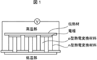
- thermoelectric conversion module As a typical thermoelectric conversion material used for the thermoelectric conversion module, for example, a thermoelectric conversion module using a material having a bulk form shown in FIG. 1 (hereinafter referred to as a bulk type thermoelectric conversion module) is known.
- a bulk type thermoelectric conversion module the process cost in the module assembling process is likely to be high, and there is a concern about the joint breakdown between the bulk material and the electrode.
- about 70% of the thermal energy discharged in power generation using fossil fuels is widely distributed as low-temperature exhaust heat of less than 200 ° C. In order to utilize such low-temperature exhaust heat as a heat source, Flexibility is required to enable installation in a narrow space and installation on a heat source member having various shapes, and there is a limit to the correspondence with bulk thermoelectric conversion modules.
- thermoelectric conversion module using a thin film thermoelectric conversion material or an organic material (hereinafter referred to as a thin film thermoelectric conversion module) is known as a thermoelectric conversion module that replaces the bulk type thermoelectric conversion module.
- the thin film type thermoelectric conversion module has the shape shown in FIG. 2 and is inferior to the bulk type thermoelectric conversion module in terms of conversion efficiency, but its assembly process cost is low and flexibility is high. It is growing. Therefore, a thin film thermoelectric conversion material that can be applied to a thin film thermoelectric conversion module and has high thermoelectric conversion efficiency is demanded.
- an iron full Heusler alloy thin film represented by Fe 2 VAl is known as a thermoelectric conversion material thin film capable of generating power with a low-temperature heat source of less than 200 ° C.
- Full Heusler alloy thin films are composed of elements that are non-toxic, inexpensive, and have a large amount of reserves, and have attracted attention in recent years from the viewpoint of environmental impact.
- Full-Heusler alloy has a high output factor as a thermoelectric performance, while it has a high thermal conductivity. In general, it is necessary to improve the crystallinity in order to increase the output factor.
- Patent Document 1 discloses a thermoelectric conversion element in which the crystallinity of a full Heusler alloy thin film is improved and a method for manufacturing the same.
- Patent Document 1 it is considered that the output factor is increased by improving the crystallinity of the full-Heusler alloy thin film as the thermoelectric conversion material thin film, and a high Seebeck coefficient and a low electrical resistivity are realized.
- the electrical resistivity decreases, the thermal conductivity contributed by the carriers inevitably increases. For this reason, in order to improve the thermoelectric performance, it is necessary to lower the thermal conductivity contributed by the crystal lattice.
- the thermal conductivity contributed by the crystal lattice tends to be reduced as the crystal grain size is reduced. Therefore, in order to reduce the thermal conductivity while realizing a high output factor in the thermoelectric conversion material thin film, it is high. It is necessary to control the crystal grain size to a desired size while maintaining crystallinity.
- an object of the present invention is to obtain a thin film thermoelectric conversion module and a manufacturing method that are excellent in thermoelectric conversion efficiency while reducing the thermal conductivity while maintaining a high output factor in the thermoelectric conversion material thin film.
- a substrate having two or more kinds of alignment regions having different crystal orientations on the surface, and a cubic crystal structure formed on the substrate are provided.
- an electrode bonded to the first thermoelectric conversion material thin film and the second thermoelectric conversion material thin film, and the first thermoelectric conversion material thin film, the second thermoelectric conversion material thin film, and the above In the insulating layer two or more kinds of alignment regions having different crystal orientations are formed adjacent to each other at positions corresponding to the positions of the alignment regions of the substrate, and the first thermoelectric conversion material thin film, the first In the thermoelectric conversion material thin film 2 and the insulating layer, Boundary between serial alignment region, a thin film thermoelectric conversion module, characterized by being formed along the boundary between the alignment regions of the substrate.
- a buffer layer is formed on a single crystal substrate, and the buffer layer formed on the single crystal substrate is annealed to have two or more different crystal orientations.
- a step of forming a substrate having an alignment region on the surface thereof, a step of forming a first thermoelectric conversion material thin film having a cubic crystal structure on the substrate, and a step of forming on the first thermoelectric conversion material thin film A step of forming an insulating layer and an electrode; a step of forming a second thermoelectric conversion material thin film having a cubic crystal structure on the insulating layer and the electrode; and the first layer formed on the substrate. And a step of annealing the laminated body having the thermoelectric conversion material thin film, the insulating layer, and the second thermoelectric conversion material thin film.
- thermoelectric conversion module and a manufacturing method that are excellent in thermoelectric conversion efficiency by reducing thermal conductivity while maintaining a high output factor in the thermoelectric conversion material thin film.
- thermoelectric conversion module 200 It is a schematic diagram of a bulk type thermoelectric conversion module. It is a schematic diagram of a thin film type thermoelectric conversion module.
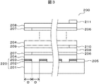
- 1 is a schematic cross-sectional view showing an example of a thin film thermoelectric conversion module 200 according to Example 1.
- FIG. It is the schematic diagram which looked at the base
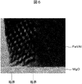
- Fe 2 VAl thin film on the MgO seed layer is a cross-section of TEM image of a film has been laminated body. It is a graph which shows the relationship between the period D of a base
- FIG. 6 is a schematic cross-sectional view showing an example of a thin film thermoelectric conversion module 300 according to Example 2.
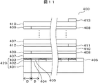
- FIG. 6 is a schematic cross-sectional view showing an example of a thin film thermoelectric conversion module 400 according to Example 3.
- FIG. 6 is a schematic cross-sectional view showing an example of a thin film thermoelectric conversion module 400 according to Example 3.
- FIG. 3 is a schematic cross-sectional view illustrating an example of the thin film thermoelectric conversion module 200 according to the first embodiment.
- an amorphous buffer layer 202 and a crystalline buffer layer 203 are stacked in this order on a single crystal substrate 201.
- the amorphous buffer layer 202 is a layer for preventing the crystal orientation of the single crystal substrate 201 from being transmitted to a layer formed above the amorphous buffer layer 202.
- the amorphous buffer layer 202 and the crystalline buffer layer 203 are A plurality of rows are provided on the single crystal substrate 201 at intervals D to form a base body 220.
- thermoelectric conversion material thin film 204 On the substrate 220, a first thermoelectric conversion material thin film 204, an insulating layer 206, a second thermoelectric conversion material thin film 208, and an insulating layer 209 are laminated in this order.
- the second thermoelectric conversion material thin film 208 is p-type when the first thermoelectric conversion material thin film 204 is n-type, and is n-type when the first thermoelectric conversion material thin film 204 is p-type. is there.
- the insulating layer 206 is provided with an electrode 207 at the end in the width direction of the interval D, and the insulating layer 209 is provided with an electrode 210 at the end in the width direction on the side facing the electrode 207.
- the electrode 207 and the electrode 210 are both provided to be joined to the first thermoelectric conversion material thin film 204 and the second thermoelectric conversion material thin film 208, and the first thermoelectric conversion material is formed by the electrode 207 and the electrode 210.
- the conductivity between the thin film 204 and the second thermoelectric conversion material thin film 208 is ensured.
- the thin film thermoelectric conversion module 200 has a periodic structure with the first thermoelectric conversion material thin film 204, the insulating layer 206 and the electrode 207, the second thermoelectric conversion material thin film 208, the insulating layer 209 and the electrode 210 as a lamination unit. Yes.
- a lower electrode 205 is provided at one end of the single crystal substrate 201, and is formed on the uppermost layer (on the second thermoelectric conversion material thin film 208 in FIG. 3) of the periodic structure formed on the single crystal substrate 201.
- Each is provided with an upper electrode 211.
- the lower electrode 205 is provided so as to be adjacent to the amorphous buffer layer 202 and the crystalline buffer layer 203, and the lower electrode 205 and the upper electrode 211 are configured so that module power can be taken out.
- the thin film thermoelectric conversion element 200 shown in FIG. 3 A specific configuration example of the thin film thermoelectric conversion element 200 shown in FIG. 3 will be described below.
- the single crystal substrate 201 a 0.5 mm thick MgO substrate having a (111) crystal orientation plane in the perpendicular direction is used.
- the amorphous buffer layer 202 is a Ta layer having a thickness of about 5 nm
- the crystalline buffer layer 203 is an MgO layer having a crystal orientation plane of (100) and a thickness of about 3 nm.
- the single crystal substrate 201 only needs to have a crystal orientation different from that of the crystalline buffer layer 203. Therefore, when MgO of the crystalline buffer layer 203 has a (100) crystal orientation plane, the single crystal substrate 201 is For example, it may have a crystal orientation plane such as (110).
- the crystalline buffer layer 203 is formed on the single crystal substrate 201 via the amorphous buffer layer 202, so that the crystalline buffer layer 203 is formed as a layer grown without being affected by the crystal orientation of the single crystal substrate 201. Yes.
- a region having a (111) crystal orientation plane of the single crystal substrate 201 hereinafter referred to as a (111) orientation region
- a (100) crystal of the crystalline buffer layer 203 are provided on the surface of the substrate 201.
- Regions having orientation planes hereinafter referred to as (100) orientation regions
- the first thermoelectric conversion material thin film 204 and the second thermoelectric conversion material thin film 208 are each formed of a full Heusler alloy obtained by substituting a part of Fe 2 VAl with Si and Ti, respectively. It is a thin film of about 200 nm.
- the insulating layers 206 and 209 are all MgO layers having a thickness of about 3 nm, and the lower electrode 205, the upper electrode 211, the electrode 207, and the electrode 210 are all Cu layers having a thickness of about 3 nm.
- the first thermoelectric conversion material thin film 204, the second thermoelectric conversion material thin film 208, the insulating layer 206, and the insulating layer 209 are all formed on the substrate 220 immediately below the first thermoelectric conversion material thin film 204. It has the same crystal orientation as the orientation region.
- the first thermoelectric conversion material thin film 204, the second thermoelectric conversion material thin film 208, the insulating layer 206, and the insulating layer 209 that are located immediately above the (111) orientation region in which the surface of the base body 220 is the single crystal substrate 201.
- Each region is a region having a crystal orientation of (111) ((111) orientation region).
- the first thermoelectric conversion material thin film 204, the second thermoelectric conversion material thin film 208, the insulating layer 206, and the insulating layer 209 existing immediately above the (100) orientation region whose surface of the substrate 220 is the crystalline buffer layer 203. These regions are all regions having a (100) crystal orientation ((100) orientation region).
- the (111) orientation region and the (100) orientation region are formed adjacent to each other. .
- the first thermoelectric conversion material thin film 204 and the second thermoelectric conversion material thin film 208 are formed of a thermoelectric conversion material having a cubic crystal structure having different carriers.
- thermoelectric conversion material for forming the first thermoelectric conversion material thin film and the second thermoelectric conversion material thin film has a cubic crystal structure and a large Seebeck coefficient, for example, a full Heusler system or a half Heusler system.
- a Heusler alloy or a chalcogenite-based alloy material can be used, and among these, a full Heusler alloy can be preferably used.
- Heusler alloys include at least one element selected from the group consisting of Fe, V, Ru, Cr, Mn, Nb, Ti, Zr, Hf, Co, and Ir, and Al, Si, Ga, Ge, Sn, In A combination of at least one element selected from the group consisting of can be used.
- Fe 2 VAl or an alloy obtained by substituting a part of the constituent elements of Fe 2 VAl with another metal element can be used.
- the constituent elements of Fe 2 VAl are replaced with other metal elements.
- Fe and V of Fe 2 VAl are any of Ru, Cr, Mn, Nb, Ti, Zr, Hf, Co, and Ir.
- Al substituted with any of Si, Ga, Ge, Sn, and In can be used.
- a part of the constituent elements of Fe 2 VAl substituted with Si and Ti can be suitably used.
- thermoelectric conversion material thin film 204 and the second thermoelectric conversion material thin film 208 are crystallized even when heat-treated at a film thickness of less than 1 nm.
- the film thicknesses of the first thermoelectric conversion material thin film 204 and the second thermoelectric conversion material thin film 208 are not less than the minimum film thickness at which crystallization is caused by heat treatment in each thin film, and film breakage due to stress strain accompanying crystallization is caused. Set to less than the minimum film thickness that results.
- the film thicknesses of the first thermoelectric conversion material thin film 204 and the second thermoelectric conversion material thin film 208 are preferably 1 nm or more and 1 ⁇ m or less.
- Single crystal substrate 201 and crystalline buffer layer 203 form part of the surface of substrate 220 and are seed films for promoting crystal growth of first thermoelectric conversion material thin film 204 or second thermoelectric conversion material thin film 208. It will be.
- the single crystal substrate 201 and the crystalline buffer layer 203 are lattice-matched with a cubic thermoelectric conversion material such as a full Heusler alloy that forms the first thermoelectric conversion material thin film 204 and the second thermoelectric conversion material thin film 208.
- An insulator having a good crystal structure can be used. Specifically, for example, any crystal structure selected from the group consisting of a perovskite structure typified by SrTiO 3 and KTaO 3 , a spinel structure typified by MgAl 2 O 4 , and a rock salt structure typified by MgO is used. The insulator which has can be used.
- the thickness of the single crystal substrate 201 is not particularly limited, but is preferably 1 mm or less from the viewpoint of ensuring the flexibility of the thin film thermoelectric conversion module 200 as a whole.
- the thickness of the crystalline buffer layer 203 is not particularly limited, but is preferably 1 nm or more and 100 nm or less from the viewpoint of maintaining stable crystallinity while ensuring the flexibility of the thin film thermoelectric conversion module 200 as a whole.
- a metal material or an inorganic material capable of forming an amorphous structure without being affected by the crystal orientation plane of the single crystal substrate 201 can be used.
- a metal material or an inorganic material capable of forming an amorphous structure without being affected by the crystal orientation plane of the single crystal substrate 201 can be used.
- Ta, Cu, Ru, Al 2 O 3 and SiO 2 are preferably used.
- the thickness of the amorphous buffer layer 202 is not particularly limited, the crystalline buffer layer 203 is not affected by the crystal orientation of the single crystal substrate 201 while ensuring the flexibility of the thin film thermoelectric conversion module 200 as a whole. From the viewpoint of securing a sufficient thickness for crystal growth, the thickness is preferably 1 nm or more and 100 nm or less.
- the insulating layers 206 and 209 ensure the insulation between the first thermoelectric conversion material thin film 204 and the second thermoelectric conversion material thin film 208, and the first thermoelectric conversion material thin film 204 or the second thermoelectric conversion material. This is a layer that becomes a seed film of the thin film 208.
- thermoelectric conversion material such as a full Heusler alloy constituting the first thermoelectric conversion material thin film 204 and the second thermoelectric conversion material thin film 208 is used.
- An insulator having a crystal structure with favorable lattice matching can be used. Specifically, for example, an insulator having a crystal structure selected from the group consisting of a perovskite structure typified by SrTiO 3 or KTaO 3 , a spinel structure typified by MgAl 2 O 4 , or a rock salt structure typified by MgO Can be used.
- the electrodes 207 and 210 ensure electrical conductivity between the first thermoelectric conversion material thin film 204 and the second thermoelectric conversion material thin film 208, and the lower electrode 205 and the upper electrode 211 are formed of a thin film thermoelectric conversion module. It is for taking out electric power from 200 outside.
- a metal material such as Cu can be suitably used from the viewpoint of ensuring good electrical conductivity.
- thermoelectric conversion element module 200 shown in FIG. 3 First, an amorphous buffer layer 202 and a crystalline buffer layer 203 are formed in this order on the single crystal substrate 201 at regular intervals D. Specifically, first, a resist is applied on a single crystal substrate 201 having a crystal orientation plane of (111) in a perpendicular direction, and the amorphous buffer layer 202 and the crystalline buffer layer 203 are formed by electron beam lithography or photolithography. The resist is removed only in the film formation region. An amorphous buffer layer 202 and a crystalline buffer layer 203 are formed in this order by sputtering in the region where the resist is removed.
- the amorphous buffer layer 202 and the crystalline buffer layer 203 are formed using an RF sputtering apparatus or a DC sputtering apparatus, and Ar gas is introduced under an ultrahigh vacuum state of 1.0 ⁇ 10 ⁇ 5 Pa or less, Sputter deposition is performed using a target of a constituent material corresponding to each layer.
- the remaining resist on the single crystal substrate 201 is removed.
- the amorphous buffer layer 202 and the crystalline buffer layer 203 remain on the single crystal substrate 201, and the surface of the single crystal substrate 201 is exposed in the region where the resist is applied.
- the crystalline buffer layer 203 formed on the single crystal substrate 201 is annealed. As a result, a crystalline buffer layer 203 having a crystal orientation of (100) different from the crystal orientation (111) of the single crystal substrate 201 is formed, and a substrate having two or more types of orientation regions having different crystal orientations on the surface 220 is obtained.
- the first thermoelectric conversion material thin film 204 is formed by sputtering on the substrate 220 thus formed, and the amorphous buffer layer 202 and the crystalline buffer layer 203 are formed on one end of the single crystal substrate 201.
- the lower electrode 205 is formed by sputtering so as to be bonded to the substrate.
- the insulating layer 206 and the electrode 207 are sequentially sputtered on the first thermoelectric conversion material thin film 204 after patterning with a resist.
- the electrode 210 is formed on the second thermoelectric conversion material thin film 208 at a position facing the electrode 207.
- the insulating layer 209 and the electrode 210 are sequentially formed by sputtering.
- thermoelectric conversion material thin film 204 the insulating layer 206 and the electrode 207
- the second thermoelectric conversion material thin film 208 the insulating layer 209
- the electrode 210 are used as constituent units, and lamination by sputtering is repeated many times.
- the first thermoelectric conversion material thin film 204 and the second thermoelectric conversion material thin film 208 at this time may have any structure of an amorphous structure, a polycrystalline structure, and a plane-oriented film.
- the first thermoelectric conversion material thin film 204 and the second thermoelectric conversion material thin film 208 are each not less than the minimum film thickness at which crystallization is caused by heat treatment in each thin film and less than the minimum film thickness at which film breakage due to stress strain accompanying crystallization occurs.
- the film thickness is, for example, 1 nm or more and 1 ⁇ m or less.
- the upper electrode 211 is formed by sputtering on the top of the stacked body (second thermoelectric conversion material thin film 208 in FIG. 3).
- the heating temperature during the annealing treatment can be approximately 800 ° C.
- the heating temperature is a temperature sufficient for crystallization of a thermoelectric conversion material having a cubic crystal structure such as a full-Heusler alloy constituting the first thermoelectric conversion material thin film 204 and the second thermoelectric conversion material thin film 208 and heat. What is necessary is just to perform in the temperature range which does not decompose
- the first thermoelectric conversion material thin film 204, the second thermoelectric conversion material thin film 208, and the insulating layers 206 and 209 have the same crystal orientation as the respective orientation regions of the base body 220 existing immediately below. Crystallization is performed with the crystal orientation, and the period of the crystal orientation of the substrate 220 is inherited by the stacked body thereon.
- the first thermoelectric conversion material thin film 204, the second thermoelectric conversion material thin film 208, and the insulating layers 206 and 209 are located immediately above the exposed surface ((111) orientation region) of the single crystal substrate 201 of the base body 220.
- the first thermoelectric conversion material thin film 204 and the second thermoelectric conversion material thin film are crystallized with a crystal orientation of (111) ((111) orientation region) and are located immediately above the crystalline buffer layer 203 in the substrate 201.
- crystallization is performed with the crystal orientation of (100) ((100) orientation region).
- the first thermoelectric conversion material thin film 204, the second thermoelectric conversion material thin film 208, and the insulating layers 206 and 209 are formed with boundaries between the alignment regions along the boundaries between the alignment regions of the substrate 220. .
- thermoelectric conversion material thin film 204 and the second thermoelectric conversion material thin film 208 using the base body 220 as a seed crystal growth of a thermoelectric conversion material such as a full Heusler alloy occurs. Crystallinity is maintained.
- the heat treatment can produce a similar structure even when crystal growth is performed with the substrate temperature raised at the time of forming each layer, but as described above, annealing is performed after forming each layer. Is preferable.
- the first thermoelectric conversion material thin film 204 and the second thermoelectric conversion material thin film 208 using the thermoelectric conversion material having the Seebeck effect that generates the potential difference by applying the temperature gradient are stacked, and further, the uppermost portion is the upper portion.
- the electrode 211 for example, when one surface of the module is heated by a heat source and the other surface is cooled by water cooling or air cooling, a temperature difference is applied to the entire module, thereby connecting to the lower electrode 205. Thus, it can be taken out as electric power.
- thermoelectric conversion efficiency of a thermoelectric conversion material is defined by a figure of merit (ZT) represented by the following formula (1).
- T is the absolute temperature
- S is the Seebeck coefficient
- ⁇ is the electrical resistivity
- ⁇ is the thermal conductivity
- thermoelectric performance in order to obtain excellent thermoelectric performance, it is effective to improve the output factor represented by the following formula (2) and reduce the thermal conductivity.
- FIG. 4 shows a schematic view of the substrate 220 of the thin film thermoelectric conversion module 200 shown in FIG. 3 as viewed from above.
- a single crystal substrate 201 ((111) orientation region) and a crystalline buffer layer 203 ((100) orientation region) are formed with a width D on the surface of the base 220, These are alternately adjacent to the direction of the heat flow from the high temperature part to the low temperature part (the direction of the temperature gradient applied to the thin film thermoelectric conversion module 200 during thermoelectric conversion) to form a periodic structure.
- thermoelectric conversion material thin film 204 and the second thermoelectric conversion material thin film 208 the interface between the alignment regions formed along the periodic structure of the substrate 220 is perpendicular to the direction of heat flow. It is formed to extend. Therefore, in the thin film thermoelectric conversion module 200, the heat flow is efficiently scattered by these interfaces, and the heat conductivity in the heat flow direction of the first thermoelectric conversion material thin film 204 and the second thermoelectric conversion material thin film 208 is reduced. . For this reason, as shown by the above formula (1), the figure of merit (ZT) of thermoelectric conversion is increased as much as the thermal conductivity is reduced.
- the width of the exposed surface of the single crystal substrate 201 shown in FIG. 4 and the widths of the amorphous buffer layer 202 and the crystalline buffer layer 203 are referred to as a base period D, and the base 220 is formed by the period.
- the width of each orientation region of the full Heusler alloy thin film in the heat flow direction is defined as the grain size of the full Heusler alloy.
- Example 1 although the width of the exposed surface of the single crystal substrate 201 and the widths of the amorphous buffer layer 202 and the crystalline buffer layer 203 are formed with the same width period D, the present invention shows It is not necessarily limited to the form in which these are formed with the same width, and the exposed surface of the single crystal substrate 201 is formed with a width larger than the width of the amorphous buffer layer 202 and the crystalline buffer layer 203 or with a small width. The formed form may be sufficient.
- thermoelectric conversion material thin film 204 the first thermoelectric conversion material thin film 204 and the second thermoelectric conversion material thin film 208 and the thermal conductivity.
- the crystal grain size dependence of thermal conductivity is expressed by the following formula (3).
- ⁇ b is the thermal conductivity inside the particle
- Ri is the interface resistance
- d is the crystal grain size.
- thermoelectric conversion material thin film formed on the substrate will be described in more detail with reference to FIG.
- a region 101 and a region 102 having crystal orientation planes different from each other are formed on the single crystal substrate 110.
- the region 104 formed on the region 101 and the region 105 formed on the region 102 have different crystal orientations. Columnar grains having properties are formed.
- each columnar grain is substantially the same as the width of the region 101 and the region 102 existing immediately below in the width direction of the substrate 120. For this reason, the width of the columnar grains of the first thermoelectric conversion material thin film 103 can be arbitrarily controlled by controlling the sizes of the region 101 and the region 102 formed in the base 120. Further, since crystal growth occurs in the first thermoelectric conversion material thin film 103 using the substrate 220 as a seed, high crystallinity is maintained in the columnar grains.
- the above formula (3) is obtained.
- the first thermoelectric conversion material thin film 204 and the second thermoelectric conversion material thin film 208 have each columnar grain so that a desired thermal conductivity can be obtained. What is necessary is just to estimate the width (the width of each alignment region).
- the width of the columnar grains of the thermoelectric conversion material thin films 204 and 208 (the width of each orientation region) is equal to the width of the period D of the base 120 existing immediately below each region, the first thermoelectric conversion material thin film 204, The desired thermal conductivity can be obtained by adjusting the width of the period D of the base 120 so that the target columnar grain width can be obtained in the second thermoelectric conversion material thin film 208.
- FIG. 6 shows a TEM image of a cross section of a laminate in which an Fe 2 VAl thin film (200 nm) is formed on an MgO seed film (thickness 3 nm).
- FIG. 6 shows the formation of Fe 2 VAl on this MgO seed film by sputtering. It is a cross-sectional image of the laminated body obtained by annealing at a predetermined temperature.
- columnar grains having different crystal orientation planes are alternately formed adjacent to each other in the Fe 2 VAl thin film.
- the columnar grains grow in the direction immediately above the crystal grains of each orientation region of the MgO seed film, and the columnar grains of the Fe 2 VAl thin film extend along the boundaries of the orientation regions of the MgO seed film. A grain boundary as a boundary is formed. Therefore, by controlling the width of each orientation region of the substrate (for example, in FIG. 4, the width of the region where the single crystal substrate 201 is exposed and the width of the region where the crystalline buffer layer 203 is formed) It can be confirmed that the particle size (width of columnar grains) of the thermoelectric conversion material thin film such as a Heusler alloy thin film grown thereon can be controlled.
- the columnar grains form an alignment region corresponding to the crystal orientation of each columnar grain in the Fe 2 VAl thin film, and the grain boundary of the columnar grains is synonymous with the boundary of each alignment region.
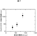
- FIG. 7 shows the relationship between the period D of the substrate and the particle size of a thermoelectric conversion material thin film (hereinafter referred to as a full Heusler alloy thin film) made of a full Heusler alloy.
- the particle diameter of the full-Heusler alloy thin film is almost the same value as the period D of the substrate, and by modulating the period D of the substrate, it can be confirmed that an arbitrary particle size can be obtained in the full-Heusler alloy thin film.
- the particle size of the full Heusler alloy thin film is the width of the columnar grain measured from a TEM image obtained by imaging the full Heusler alloy thin film with a TEM.
- FIG. 8 shows the relationship between the particle size of the full-Heusler alloy thin film and the thermal conductivity.
- black circles are measured values (examples) of the thermal conductivity of the full Heusler alloy thin film formed on the substrate having the periodic structure of the period D, and the triangular marks are the period on the single crystal substrate. It is a measured value (comparative example) of the thermal conductivity of a full Heusler alloy thin film when a full Heusler alloy thin film is laminated
- the thermal conductivity is about 10 ⁇ m (comparative example). Compared with the thermal conductivity at that time, it decreased to 4.5 W / mK, which is about 1/6.
- FIG. 9 shows the relationship between the particle size of the full-Heusler alloy thin film and the integrated values of thermal conductivity and electrical resistivity.
- the integrated values of thermal conductivity and electrical resistivity decrease monotonically with decreasing grain size of the full Heusler alloy thin film, and electrical resistance with decreasing grain size (increasing the number of grain boundaries) of the full Heusler alloy thin film.
- the increase in rate has little effect on the integrated value of thermal conductivity and electrical resistivity, and by reducing the particle size, the figure of merit (ZT) of the full Heusler alloy thin film is improved from the above formula (1). It can be confirmed.
- thermoelectric conversion module 200 In the thin film thermoelectric conversion module 200 according to the first embodiment described above, two or more types of orientation regions having different crystal orientations are formed on the surface of the base body 220, and the first thermoelectric layer laminated on the base body 220 is formed.
- the conversion material thin film 204 and the second thermoelectric conversion material thin film 208 two or more types of alignment regions having different crystal orientations are formed for each alignment region of the substrate 220, and between these alignment regions, A boundary extending along the boundary between the alignment regions is formed.
- thermoelectric conversion material thin film full Heusler alloy thin film
- thermoelectric conversion efficiency of the thin film type thermoelectric conversion module 200 with the substrate period D set to 30 nm is about 4 when the low temperature heat source is set to 50 ° C. and the high temperature heat source is set to 200 ° C. 0.0%.
- a P-type thermoelectric conversion material thin film (first thermoelectric conversion material thin film) is used instead of a substitute of Fe 2 VAl with Si and Ti.
- Fe 2 VAl with about 2% less Fe was used.
- the first thermoelectric conversion material thin film 204 is formed without forming the amorphous buffer layer 202 and the crystalline buffer layer 203. Otherwise, the thin film type thermoelectric conversion shown in FIG.
- the thin film thermoelectric conversion module having the same configuration as that of the module 200 has a thermoelectric conversion efficiency of about 0.2%. That is, in the structure in which the periodic structure is formed on the base body 220, the thermoelectric conversion efficiency is increased by 3.8% compared to the structure in which the periodic structure is not formed.
- FIG. 10 is a schematic cross-sectional view illustrating an example of the thin film thermoelectric conversion module 300 according to the second embodiment.
- an amorphous buffer layer 302 and a crystalline buffer layer 303 are embedded in this order in a single crystal substrate 301.
- the amorphous buffer layer 302 and the crystalline buffer layer 303 are embedded in a plurality of rows at intervals D in the width direction of the single crystal substrate 301, and the surface of the crystalline buffer layer 303 is combined with the surface of the single crystal substrate 301.
- a base 320 is formed so as to form a flat surface.
- thermoelectric conversion material thin film 304 is formed on the surface of the base 320 formed flat in this way, on which an insulating layer 306 and an electrode 307, a second thermoelectric conversion material thin film 308, an insulating layer are formed. 309 and the electrode 310 are stacked in this order.
- a periodic structure is formed using the first thermoelectric conversion material thin film 304, the insulating layer 306 and the electrode 307, the second thermoelectric conversion material thin film 308, the insulating layer 309 and the electrode 310 as a lamination unit.
- a lower electrode 305 is provided at one end of the single crystal substrate 301, and an upper electrode 311 is provided on the uppermost layer (on the second thermoelectric conversion material thin film 308 in FIG. 10) of the periodic structure formed on the single crystal substrate 301.
- the lower electrode 305 and the upper electrode 311 are configured so that the power of the module can be taken out.
- the film thickness of the full Heusler alloy thin film 304 is set to the film thickness of the amorphous buffer layer 302 and the film thickness of the crystalline buffer layer 303. Even when it is smaller than the total film thickness, the thin film thermoelectric conversion module 300 having the base 320 and the periodic structure of the laminate formed on the base 320 can be obtained. Further, according to the thin film thermoelectric conversion module 300 of the second embodiment, the first thermoelectric conversion material thin film 304 can be formed on the base 320 having a flat surface, so that the outermost surface of the thin film thermoelectric conversion module 300 is flat. And the reliability as a product can be improved.
- each layer The functions and constituent materials of each layer are the same as those of the thin film thermoelectric conversion module 200 (see FIG. 3) of the first embodiment, and the description thereof is omitted.
- an amorphous buffer layer 302 and a crystalline buffer layer 303 are formed by sputtering in a recess formed by polishing a single crystal substrate 301 by an ion milling method.
- the first thermoelectric conversion material thin film 304, the insulating layer 306 and the electrode 307, the second thermoelectric conversion material thin film 308, the insulating layer 309 and the electrode 310, the lower electrode 305, and the upper electrode 311 are sputtered on the substrate 320. It can be obtained by forming a film.
- FIG. 11 is a schematic cross-sectional view illustrating an example of the thin film thermoelectric conversion module 400 according to the third embodiment.
- an amorphous buffer layer 402 and an orientation control layer 404 are alternately stacked adjacent to each other on a single crystal substrate 401, and the crystalline buffer layer 402 is formed on the amorphous buffer layer 402.
- the crystalline buffer layer 405 is laminated on the orientation control layer 404 and the layer 403.
- the amorphous buffer layer 402 is a layer for preventing the crystal orientation of the single crystal substrate 401 from being transmitted to the layer formed on the upper side.
- the orientation control layer 404 transmits the crystal orientation of the single crystal substrate 201 to, for example, a layer formed on the upper side of the orientation control layer 404, thereby forming a layer formed on the upper side of the orientation control layer 404.
- This is a layer for making the crystal orientation plane different from the crystal orientation plane of the crystalline buffer layer 403.
- the orientation control layer 404 it is only necessary that the crystal orientation plane of the crystalline buffer layer 405 formed thereon can be different from the crystal orientation plane of the crystalline buffer layer 403.
- the single crystal substrate 401 The crystal orientation plane can be transferred to the crystalline buffer layer 405 and can be a layer made of Fe, Co, Ag, Pt, or a mixture thereof.
- the stacked body including the amorphous buffer layer 402 and the crystalline buffer layer 403 and the stacked body including the orientation control layer 404 and the crystalline buffer layer 405 are alternately adjacent to each other with a period D on the single crystal substrate 401.
- a base body 420 having a flat surface is formed.
- thermoelectric conversion material thin film 407 On the base 420, a first thermoelectric conversion material thin film 407, an insulating layer 408 and an electrode 409, a second thermoelectric conversion material thin film 410, an insulating layer 412 and an electrode 411 are laminated in this order.
- a periodic structure is formed using the first thermoelectric conversion material thin film 407, the insulating layer 408 and the electrode 409, the second thermoelectric conversion material thin film 410, the insulating layer 412 and the electrode 411 as a lamination unit.
- a lower electrode 406 is provided at one end of the single crystal substrate 401, and is formed on the uppermost layer (on the second thermoelectric conversion material thin film 410 in FIG. 11) of the periodic structure formed on the single crystal substrate 401.
- Each is provided with an upper electrode 413, and the lower electrode 406 and the upper electrode 413 are configured so that the power of the module can be taken out.
- each layer other than the orientation control layer 404 is the same as those of the thin film thermoelectric conversion module 200 (see FIG. 3) of Example 1, and the description thereof is omitted.
- the thin film thermoelectric conversion module 400 shown in FIG. 11 As the single crystal substrate 401, a 0.5 mm thick MgO substrate having a (111) crystal orientation plane in the perpendicular direction is used.
- the amorphous buffer layer 402 is a Ta layer having a thickness of about 5 nm
- the crystalline buffer layer 403 is MgO having a (100) crystal orientation plane and a thickness of about 3 nm.
- the orientation control layer 404 is an Fe layer having a (111) crystal orientation plane and a thickness of about 5 nm
- the crystalline buffer layer 405 is an MgO layer having a (111) crystal orientation plane and a thickness of about 3 nm. is there.
- the crystalline buffer layer 403 has a crystalline region having the same crystal orientation as the region having the (100) crystal orientation plane ((100) orientation region) and the crystal orientation of the single crystal substrate 401.
- the regions having the (111) crystal orientation plane of the buffer layer 405 ((111) orientation regions) are alternately formed with a period D.
- the first thermoelectric conversion material thin film 407 and the second thermoelectric conversion material thin film 410 are each formed of a full Heusler alloy obtained by substituting a part of Fe 2 VAl with Si and Ti, respectively, and each has a thickness. It is a thin film of about 200 nm.
- the film thicknesses of the first thermoelectric conversion material thin film 407 and the second thermoelectric conversion material thin film 410 are equal to or greater than the minimum film thickness at which crystallization is caused by heat treatment in each thin film, as in Example 1, and the stress accompanying crystallization. It is preferable to set the film thickness to be less than the minimum film thickness at which film breakage due to strain occurs.
- the film thickness is preferably 1 nm to 1 ⁇ m.
- the insulating layers 408 and 412 are all MgO layers having a thickness of about 3 nm, and the lower electrode 406, the upper electrode 413, the electrode 409, and the electrode 411 are all Cu layers having a thickness of about 3 nm.
- thermoelectric conversion module 400 the first thermoelectric conversion material thin film 407, the second thermoelectric conversion material thin film 410, and the insulating layers 408 and 412 are all formed with the crystal orientation plane of the base 420 existing immediately below. Grows in the same crystal orientation plane.
- crystallization is performed with a crystal orientation of (111) by annealing after the stacked body is formed.
- thermoelectric conversion material thin film 407 the first thermoelectric conversion material thin film 407, the second thermoelectric conversion material thin film 410, and the insulating layers 408 and 412 have respective crystallographic regions whose boundaries are formed on the surface of the base 420. It is formed along the boundary.
- the above-described thin film thermoelectric conversion module 400 can be produced by the same method as the thin film thermoelectric conversion module 200 of Example 1, and the description thereof is omitted.
- thermoelectric conversion efficiency of the thin film thermoelectric conversion module 400 with the substrate period D set to 30 nm was about 4.0% when the low temperature heat source was set to 50 ° C. and the high temperature heat source was set to 200 ° C.
- thermoelectric conversion material thin film 407 and the second thermoelectric conversion material thin film 410 are replaced with a P-type thermoelectric conversion material thin film (first thermoelectric conversion material thin film) instead of a substitute of Fe 2 VAl with Si and Ti.
- first thermoelectric conversion material thin film a substitute of Fe 2 VAl with Si and Ti.
- Fe: V: Al 2: 1: the Fe 2 VAl of Fe is one used after about 2% more, N-type thermoelectric conversion material film (second thermoelectric conversion material thin film 410 ) Fe 2 VAl with about 2% less Fe was used.
- the first thermoelectric conversion material thin film 407 is formed on the single crystal substrate 401 without forming the amorphous buffer layer 402, the crystalline buffer layer 403, the orientation control layer 404, and the crystalline buffer layer 405.
- the thermoelectric conversion efficiency was about 0.2%. That is, in the structure in which the periodic structure is formed on the base body 420, the thermoelectric conversion efficiency is increased by 3.8% compared to the structure in which the periodic structure is not formed.
- thermoelectric conversion module 400 of Example 3 since the first thermoelectric conversion material thin film 407 can be formed on the base 420 having a flat surface, the flatness of the outermost surface of the thin film thermoelectric conversion module 400 is improved. The reliability of the product can be improved.
Landscapes
- Engineering & Computer Science (AREA)
- Manufacturing & Machinery (AREA)
- Physical Vapour Deposition (AREA)
Abstract
L'invention concerne un module de conversion thermoélectrique à couches minces qui présente un excellent rendement de conversion thermoélectrique par réduction de la conductivité thermique d'une couche mince de matériau de conversion thermoélectrique, tout en maintenant un facteur de sortie élevé de cette dernière. Un module de conversion thermoélectrique à couches minces (200) est décrit, qui comprend : une base (220) qui comporte au moins deux régions d'orientation dans sa surface, lesdites régions d'orientation ayant des orientations cristallines différentes l'une de l'autre; une première couche mince de matériau de conversion thermoélectrique (204) qui est formée sur la base (220) et présente une structure cristalline cubique; une seconde couche mince de matériau de conversion thermoélectrique (208); une couche isolante (206) qui est formée sur la première couche mince de matériau de conversion thermoélectrique (204); et des électrodes (207, 210). La première couche mince de matériau de conversion thermoélectrique (204), la seconde couche mince de matériau de conversion thermoélectrique (208) et la couche isolante (206) comportent respectivement au moins deux régions d'orientation, qui sont formées adjacentes l'une à l'autre et ont des orientations cristallines différentes l'une de l'autre, à des positions correspondant aux régions d'orientation de la base (220); et les frontières entre les régions d'orientation sont formées le long de la frontière entre les régions d'orientation de la base (220).
Priority Applications (1)
| Application Number | Priority Date | Filing Date | Title |
|---|---|---|---|
| PCT/JP2015/053813 WO2016129082A1 (fr) | 2015-02-12 | 2015-02-12 | Module de conversion thermoélectrique à couches minces et son procédé de fabrication |
Applications Claiming Priority (1)
| Application Number | Priority Date | Filing Date | Title |
|---|---|---|---|
| PCT/JP2015/053813 WO2016129082A1 (fr) | 2015-02-12 | 2015-02-12 | Module de conversion thermoélectrique à couches minces et son procédé de fabrication |
Publications (1)
| Publication Number | Publication Date |
|---|---|
| WO2016129082A1 true WO2016129082A1 (fr) | 2016-08-18 |
Family
ID=56615445
Family Applications (1)
| Application Number | Title | Priority Date | Filing Date |
|---|---|---|---|
| PCT/JP2015/053813 Ceased WO2016129082A1 (fr) | 2015-02-12 | 2015-02-12 | Module de conversion thermoélectrique à couches minces et son procédé de fabrication |
Country Status (1)
| Country | Link |
|---|---|
| WO (1) | WO2016129082A1 (fr) |
Cited By (1)
| Publication number | Priority date | Publication date | Assignee | Title |
|---|---|---|---|---|
| US20180287037A1 (en) * | 2017-03-30 | 2018-10-04 | Tdk Corporation | Laminate and thermoelectric conversion element |
Citations (2)
| Publication number | Priority date | Publication date | Assignee | Title |
|---|---|---|---|---|
| JP2013522861A (ja) * | 2011-02-22 | 2013-06-13 | パナソニック株式会社 | 熱電変換素子とその製造方法 |
| WO2013114592A1 (fr) * | 2012-02-01 | 2013-08-08 | 富士通株式会社 | Élément de conversion thermoélectrique, et procédé de fabrication de celui-ci |
-
2015
- 2015-02-12 WO PCT/JP2015/053813 patent/WO2016129082A1/fr not_active Ceased
Patent Citations (2)
| Publication number | Priority date | Publication date | Assignee | Title |
|---|---|---|---|---|
| JP2013522861A (ja) * | 2011-02-22 | 2013-06-13 | パナソニック株式会社 | 熱電変換素子とその製造方法 |
| WO2013114592A1 (fr) * | 2012-02-01 | 2013-08-08 | 富士通株式会社 | Élément de conversion thermoélectrique, et procédé de fabrication de celui-ci |
Cited By (2)
| Publication number | Priority date | Publication date | Assignee | Title |
|---|---|---|---|---|
| US20180287037A1 (en) * | 2017-03-30 | 2018-10-04 | Tdk Corporation | Laminate and thermoelectric conversion element |
| US10629796B2 (en) | 2017-03-30 | 2020-04-21 | Tdk Corporation | Laminate and thermoelectric conversion element |
Similar Documents
| Publication | Publication Date | Title |
|---|---|---|
| JP5692329B2 (ja) | 圧電薄膜素子 | |
| KR101956278B1 (ko) | 그래핀 함유 복합 적층체, 이를 포함하는 열전재료, 열전모듈과 열전 장치 | |
| JP6907323B2 (ja) | 多層薄膜およびその調製 | |
| JP5230116B2 (ja) | 高配向性シリコン薄膜の形成方法、3次元半導体素子の製造方法及び3次元半導体素子 | |
| CN101032038B (zh) | 热电转换器件、以及使用该热电转换器件的冷却方法和发电方法 | |
| US20190198313A1 (en) | Flexible Single-Crystal Semiconductor Heterostructures and Methods of Making Thereof | |
| KR20150141139A (ko) | 수소 원자 또는 수소 이온을 함유하는 단결정 금속막 및 그 제조방법 | |
| JP2006196577A (ja) | 配向性熱電薄膜の製造方法及び配向性熱電薄膜を有する半導体デバイス | |
| KR101837828B1 (ko) | 열전 재료, 이의 제조 방법 및 열전 소자 | |
| US20110100408A1 (en) | Quantum well module with low K crystalline covered substrates | |
| JP6502193B2 (ja) | シリコン微結晶複合体膜、熱電材料及びそれらの製造方法 | |
| US20100269879A1 (en) | Low-cost quantum well thermoelectric egg-crate module | |
| CN101969096A (zh) | 纳米结构热电材料、器件及其制备方法 | |
| WO2016129082A1 (fr) | Module de conversion thermoélectrique à couches minces et son procédé de fabrication | |
| JP3626169B2 (ja) | 熱電変換材料およびその製造方法 | |
| EP3151292B1 (fr) | Structure thermoélectrique, dispositif thermoélectrique et son procédé de fabrication | |
| JPH11330569A (ja) | 熱電変換素子およびその製造方法 | |
| JP5834871B2 (ja) | 熱電変換素子及びその製造方法 | |
| JP5185051B2 (ja) | 熱電変換材料の製造方法 | |
| CN106350773B (zh) | 一种增大层状钴基氧化物薄膜高温热电势的方法 | |
| JP2004307310A (ja) | Fe−Si系薄膜の作製方法及びFe−Si系薄膜 | |
| JP2005350735A (ja) | 酸化物薄膜の製作方法、圧電膜および液体吐出ヘッド | |
| TWI827204B (zh) | 結晶化積層結構體之製造方法 | |
| KR20140021510A (ko) | 열전 변환 구조체 및 그 제조 방법 | |
| CN112864300A (zh) | 一种碲化铋基合金薄膜-钙钛矿型氧化物异质结复合热电材料及其制备与应用 |
Legal Events
| Date | Code | Title | Description |
|---|---|---|---|
| 121 | Ep: the epo has been informed by wipo that ep was designated in this application |
Ref document number: 15881957 Country of ref document: EP Kind code of ref document: A1 |
|
| NENP | Non-entry into the national phase |
Ref country code: DE |
|
| 122 | Ep: pct application non-entry in european phase |
Ref document number: 15881957 Country of ref document: EP Kind code of ref document: A1 |
|
| NENP | Non-entry into the national phase |
Ref country code: JP |