WO2013115074A1 - Dispositif et procédé de démodulation et programme - Google Patents
Dispositif et procédé de démodulation et programme Download PDFInfo
- Publication number
- WO2013115074A1 WO2013115074A1 PCT/JP2013/051526 JP2013051526W WO2013115074A1 WO 2013115074 A1 WO2013115074 A1 WO 2013115074A1 JP 2013051526 W JP2013051526 W JP 2013051526W WO 2013115074 A1 WO2013115074 A1 WO 2013115074A1
- Authority
- WO
- WIPO (PCT)
- Prior art keywords
- channel
- unit
- signal
- input signal
- frequency
- Prior art date
- Legal status (The legal status is an assumption and is not a legal conclusion. Google has not performed a legal analysis and makes no representation as to the accuracy of the status listed.)
- Ceased
Links
Images




Classifications
-
- H—ELECTRICITY
- H03—ELECTRONIC CIRCUITRY
- H03D—DEMODULATION OR TRANSFERENCE OF MODULATION FROM ONE CARRIER TO ANOTHER
- H03D3/00—Demodulation of angle-, frequency- or phase- modulated oscillations
- H03D3/007—Demodulation of angle-, frequency- or phase- modulated oscillations by converting the oscillations into two quadrature related signals
-
- H—ELECTRICITY
- H04—ELECTRIC COMMUNICATION TECHNIQUE
- H04L—TRANSMISSION OF DIGITAL INFORMATION, e.g. TELEGRAPHIC COMMUNICATION
- H04L1/00—Arrangements for detecting or preventing errors in the information received
- H04L1/004—Arrangements for detecting or preventing errors in the information received by using forward error control
- H04L1/0045—Arrangements at the receiver end
- H04L1/0047—Decoding adapted to other signal detection operation
-
- H—ELECTRICITY
- H04—ELECTRIC COMMUNICATION TECHNIQUE
- H04L—TRANSMISSION OF DIGITAL INFORMATION, e.g. TELEGRAPHIC COMMUNICATION
- H04L27/00—Modulated-carrier systems
- H04L27/18—Phase-modulated carrier systems, i.e. using phase-shift keying
- H04L27/22—Demodulator circuits; Receiver circuits
-
- H—ELECTRICITY
- H04—ELECTRIC COMMUNICATION TECHNIQUE
- H04L—TRANSMISSION OF DIGITAL INFORMATION, e.g. TELEGRAPHIC COMMUNICATION
- H04L27/00—Modulated-carrier systems
- H04L27/32—Carrier systems characterised by combinations of two or more of the types covered by groups H04L27/02, H04L27/10, H04L27/18 or H04L27/26
- H04L27/34—Amplitude- and phase-modulated carrier systems, e.g. quadrature-amplitude modulated carrier systems
- H04L27/38—Demodulator circuits; Receiver circuits
-
- H—ELECTRICITY
- H03—ELECTRONIC CIRCUITRY
- H03D—DEMODULATION OR TRANSFERENCE OF MODULATION FROM ONE CARRIER TO ANOTHER
- H03D2200/00—Indexing scheme relating to details of demodulation or transference of modulation from one carrier to another covered by H03D
- H03D2200/0041—Functional aspects of demodulators
- H03D2200/005—Analog to digital conversion
-
- H—ELECTRICITY
- H04—ELECTRIC COMMUNICATION TECHNIQUE
- H04L—TRANSMISSION OF DIGITAL INFORMATION, e.g. TELEGRAPHIC COMMUNICATION
- H04L27/00—Modulated-carrier systems
- H04L27/0014—Carrier regulation
- H04L2027/0044—Control loops for carrier regulation
- H04L2027/0063—Elements of loops
- H04L2027/0065—Frequency error detectors
Definitions
- the present technology relates to a demodulating device, a demodulating method, and a program, and in particular, demodulation in which demodulation processing can be realized at the same speed as when the I channel and Q channel are inverted even when they are not inverted.
- the present invention relates to an apparatus, a demodulation method, and a program.
- Patent Document 2 proposes a technique for quickly detecting channel inversion.
- the channel control unit can switch the channel of the input signal at the timing when the frame of the input signal switches.
- the channel control unit can switch the channel of the input signal again when the frame of the input signal is not established within a predetermined time after switching the channel of the input signal.
- a demodulation method is a demodulation method of a demodulator that demodulates an input signal separated into two signals of an I channel and a Q channel, and corrects the frequency of the input signal to obtain the frequency.
- a frequency correction process to be synchronized is performed, an inversion detection process for detecting that the I channel and the Q channel as the input signals are inverted, and the I channel and the Q channel are detected by the inversion detection process.
- the method includes a step of performing channel control processing for switching the I channel and the Q channel in processing subsequent to the frequency correction processing.
- the demodulation process can be realized at the same speed as when there is no inversion. .
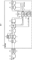
- FIG. 1 It is a block diagram which shows the structural example of one Embodiment of the demodulation apparatus to which this technique is applied. It is a figure which shows the mapping pattern on the complex plane of each symbol in (pi) / 2 shift BPSK.
- 3 is a flowchart for explaining a demodulation process executed by the demodulation device of FIG. 1.
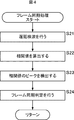
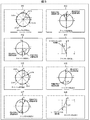
- 2 is a flowchart for explaining frame synchronization processing executed by the demodulator of FIG. 1. Relation between presence / absence of channel inversion of input signal, reception point on complex plane when receiving known sequence inserted in input signal, received delay detection value of received sequence corresponding to known sequence and known delay detection value
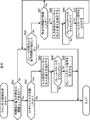
- FIG. 2 is a flowchart for explaining channel control processing executed by the demodulating device of FIG. 1.
- the DVB-S.2 standard is a standard that is standardized by the ETSI (European Telecommunications Standards Organization) and corresponds to the higher rank of the DVB-S standard being used.
- the DVB-S.2 standard introduces multi-level phase modulation and LDPC (Low Density Parity Check) codes to improve frequency utilization efficiency per unit frequency and C / N ratio ( Carrier to Noise ratio) is being improved.
- LDPC Low Density Parity Check
- C / N ratio Carrier to Noise ratio
- a PL (physical layer) header for transmitting physical layer transmission information and a synchronous pilot signal have been introduced as standards.
- FIG. 2 shows a mapping pattern on the complex plane of each symbol in ⁇ / 2 shift BPSK.
- the left side of FIG. 2 shows a mapping pattern of odd-numbered symbols, and the right side shows a mapping pattern of even-numbered symbols. That is, on the complex plane, odd-numbered symbols are mapped to points with a declination of ⁇ / 4 when the value is 0, and are mapped to points with a declination of 5 ⁇ / 4 when the value is 1.
- the second symbol is mapped to a point having a declination angle of 3 ⁇ / 4.
- the second symbol is mapped to a point having a declination angle of 7 ⁇ / 4. Therefore, the phase difference between adjacent symbols is limited to ⁇ ⁇ / 2.
- the reception system is configured to include an antenna 11, a tuner 12, A / D converters 13-1 and 13-2, and a demodulator 14.
- the tuner 12 receives an input signal conforming to the DVB-S.2 standard via the antenna 11 and separates the received input signal into two signals of an I channel and a Q channel, and each of them is an A / D converter 13- 1 and 13-2.
- the I channel signal is also referred to as an I channel signal
- the Q channel signal is also referred to as a Q channel signal.
- the demodulator 14 includes a frequency correction unit 31, a frequency synchronization unit 32, a clock synchronization unit 33, a reception filter 34, a channel inversion control unit 35, an equalizer 36, a frame synchronization unit 37, a phase synchronization unit 38, and an error correction unit 39. including.
- the frequency correction unit 31 corrects the frequency of the input signal based on the correction signal supplied from the frequency synchronization unit 32 and supplies the corrected signal to the clock synchronization unit 33.
- the clock synchronization unit 33 synchronizes the input signal whose frequency is corrected by the frequency correction unit 31 with the clock signal, and supplies it to the frequency synchronization unit 32 and the reception filter 34.
- the frequency synchronization unit 32 obtains a correction amount required to synchronize the frequency of the input signal with a predetermined frequency, and supplies it to the frequency correction unit 31 as a correction signal. That is, the frequency of the input signal and the clock synchronization are established by the loop of the frequency correction unit 31, the frequency synchronization unit 32, and the clock synchronization unit 33.
- the reception filter 34 is, for example, a roll-off filter, and supplies the filtering result to the channel inversion control unit 35.
- the channel inversion control unit 35 switches the I channel signal and the Q channel signal that are input signals supplied from the reception filter 34 based on the channel inversion detection result supplied from the channel inversion detection unit 51 of the frame synchronization unit 37. Output. Further, the channel inversion control unit 35 receives the frame start signal supplied from the frame synchronization determination unit 53 of the frame synchronization unit 37 when it is necessary to exchange the I channel signal and the Q channel signal based on the channel inversion detection result. At the acquired timing, the I channel signal and the Q channel signal are switched and supplied to the equalizer 36.
- the frame synchronization unit 37 performs synchronization control in units of frames with respect to the input signal.
- the frame synchronization unit 37 supplies the input signal supplied from the equalizer 36 to the phase synchronization unit 38 as it is.
- the frame synchronization unit 37 includes a channel inversion detection unit 51, a correlation detection unit 52, and a frame synchronization determination unit 53, and performs channel control along with synchronization control.
- the channel inversion detection unit 51 determines whether the phase of the I channel and the Q channel of the signal output to the phase synchronization unit 38 is correct, that is, whether the phase of the Q channel is delayed by ⁇ / 2 with respect to the I channel. Is detected. More specifically, the channel inversion detection unit 51 includes a correlation value from the correlation detection unit 52, a determination result of reliability of the correlation value, a frame synchronization state notified from the frame synchronization determination unit 53, or an error correction unit. Based on the state of decoding synchronization by error correction processing notified from 39, it is detected whether or not the phases of the I channel and the Q channel are in a correct relationship. The channel inversion detection unit 51 supplies the detection result to the channel inversion control unit 35 as the channel inversion detection result. Based on the channel inversion detection result, the channel inversion control unit 35 exchanges the channel of the input signal when the phase is not in a correct relationship and needs to be exchanged.
- Correlation with a symbol sequence (hereinafter also referred to as a known delay detection sequence) of a correct delay detection value (hereinafter also referred to as a known delay detection value) of a symbol sequence (hereinafter also referred to as a known sequence), and a correlation obtained as a result
- the value is supplied to the channel inversion detection unit 51 and the frame synchronization determination unit 53.
- the correlation detection unit 52 determines the reliability of the correlation value and notifies the channel inversion detection unit 51 of the determination result.
- the correlation detection unit 52 uses the SOF (Start Of Frame) of the PL header inserted at the head of each header of the input signal as a known sequence, and a known delayed detection sequence and reception delay detection corresponding to the known sequence. A description will be given assuming that the correlation value between the sequences is calculated.
- SOF Start Of Frame
- the frame synchronization determination unit 53 detects the peak value of the correlation value that appears in the frame period and its timing (hereinafter also referred to as peak timing).
- the phase synchronization unit 38 corrects the phase error of each symbol of the input signal and supplies it to the error correction unit 39.
- the error correction unit 39 performs error correction processing (FEC (Forward Error Correction)) such as LDPC and BCH decoding or Viterbi decoding and Reed-Solomon decoding on the input signal, and TS (Transport) obtained as a result Stream) packet is output to the subsequent device. Further, the error correction unit 39 supplies a signal indicating the decoding synchronization state by the error correction decoding process to the channel inversion detection unit 51 of the frame synchronization unit 37.
- FEC Forward Error Correction
- step S1 the tuner 12 receives an input signal compliant with the DVB-S.2 standard via the antenna 11, separates the received input signal into two signals of I channel and Q channel, and performs A / D conversion. To the devices 13-1 and 13-2.
- step S2 the A / D converters 13-1 and 13-2 A / D convert the input I channel signal or Q channel signal from an analog signal to a digital signal, and the converted signal is demodulated by the demodulator 14. To the frequency correction unit 31.
- step S3 the frequency correction unit 31 corrects the frequencies of the I channel signal and the Q channel signal that are converted into digital signals and input based on the correction signal indicating the correction amount supplied from the frequency synchronization unit 32. To the clock synchronizer 33.
- step S4 the clock synchronization unit 33 synchronizes the I channel signal and Q channel signal, which are supplied from the frequency correction unit 31 and corrected for the frequency converted into the digital signal, with a predetermined clock signal.
- the data is supplied to the synchronization unit 32 and the reception filter 34.
- step S5 the frequency synchronization unit 32 generates a signal indicating the frequency correction amount of the I channel signal and the Q channel signal with which the clocks are synchronized, and supplies the signal to the frequency correction unit 31.
- the same processing is repeated by the loop constituted by the frequency correction unit 31, the frequency synchronization unit 32, and the clock synchronization unit 33, so that the synchronization of the frequency and the clock is established.
- the established state is continued.
- step S 6 the reception filter 34 applies, for example, a roll-off filter to the channel inversion control unit 35 by applying a roll-off filter to the I channel signal and the Q channel signal synchronized in frequency with the clock supplied from the clock synchronization unit 33. To do.
- step S ⁇ b> 7 the channel inversion control unit 35 determines whether or not a channel inversion detection result indicating that the I channel signal and the Q channel signal are inverted is supplied from the channel inversion detection unit 51 of the frame synchronization unit 37. Determine.
- step S8 for example, step S63.
- the process proceeds to step S8.
- step S9 the channel inversion control unit 35 inverts the I channel signal and the Q channel signal supplied from the reception filter 34 and supplies them to the equalizer 36.
- step S22 the correlation detection unit 52 calculates a correlation value. Specifically, the correlation detection unit 52 calculates a correlation value representing the correlation between the received delay detection sequence and the known delay detection sequence based on the following equation (1).
- K is a value obtained by subtracting 1 from the number of symbols of a known sequence inserted at the beginning of each frame of the input signal.
- D i represents the i-th value of the received delay detection sequence.
- the correlation detection unit 52 supplies the calculated correlation value to the channel inversion detection unit 51 and the frame synchronization determination unit 53.
- the phase rotates by + ⁇ with respect to the delay detection value of the known series (known delay detection value).
- the correlation value between the known delay detection sequence and the received delay detection sequence corresponding to the known sequence that is, the correlation value at the peak timing is expressed by the following equation (2) based on the above equation (1). .
- the reception delay detection value and the known delay detection value corresponding to the known sequence have the value of ⁇ as shown in the complex planes H2 and H3 in FIG. The smaller the value, the closer to the same phase and the stronger the positive correlation.
- the correlation value at the peak timing is Ke j ( ⁇ / 2 + ⁇ ) (K is a value obtained by subtracting 1 from the number of symbols in the known sequence as in the equation (1)).
- K is a value obtained by subtracting 1 from the number of symbols in the known sequence as in the equation (1).
- 5 complex plane H4 it can be expressed with an angle of + ⁇ with respect to the positive direction of the Q axis.
- the phase rotates by ⁇ with respect to the known delay detection value of the known series.
- the correlation value between the known delay detection sequence and the received delay detection sequence corresponding to the known sequence is expressed by the following equation (3) based on the above equation (1).
- the known delay detection value and the reception delay detection value corresponding to the known sequence have a value of ⁇ .
- step S14 the error correction unit 39 performs error correction processing (FEC (Forward Error Correction)) such as LDPC and BCH decoding or Viterbi decoding and Reed-Solomon decoding on the input signal, and the result is obtained.
- FEC Forward Error Correction
- a TS (transport stream) packet is output to a subsequent apparatus.
- the error correction unit 39 supplies a signal indicating the decoding synchronization state by the error correction decoding process to the channel inversion detection unit 51 of the frame synchronization unit 37.
- step S15 the tuner 12 determines whether or not the next signal is received via the antenna 11, and if it is determined that there is a next signal, the process returns to step S1 and the subsequent processes are performed. Is repeated. If it is determined in step S15 that there is no next signal, the process ends.
- the channel inversion control unit 35 is provided in the subsequent stage of the configuration for establishing the synchronization of the frequency and the clock signal, that is, in the subsequent stage of the frequency synchronization unit 32 and the clock synchronization unit 33. For this reason, even when the replacement of the I channel signal and the Q channel signal is instructed, the channel inversion control unit 35 can switch the channels while maintaining the synchronization of the frequency and the clock signal. It becomes. As a result, in the demodulation process, even if the I channel signal and the Q channel signal are inverted, it is not necessary to establish the synchronization of the frequency and the clock accompanying the replacement of the I channel signal and the Q channel signal. Therefore, it is possible to realize demodulation processing in substantially the same processing time as when no inversion of the I channel signal and the Q channel signal occurs.
- step S62 the channel inversion detection unit 51 determines whether the I channel signal and the Q channel of the input signal are inverted. More specifically, the channel inversion detection unit 51 determines whether the I channel signal and the Q channel of the input signal are inverted by determining whether the value of the imaginary part of the correlation value is 0 or more.
- the correlation value at the peak timing is Ke j ( ⁇ / 2 + ⁇ ) in an ideal reception environment.
- the correlation value at the peak timing is Ke j ( ⁇ / 2 ⁇ in an ideal reception environment. ) . Therefore, when the channel of the input signal is not inverted, when ⁇ is within the range of ⁇ ⁇ / 2, as shown by the shaded portion in the left diagram of FIG. 7, the imaginary part of the correlation value at the peak timing is shown.
- the value is positive, and the correlation between the known delayed detection sequence and the received delayed detection sequence corresponding to the known sequence is a positive correlation.
- the channel of the input signal is inverted, when ⁇ is within the range of ⁇ ⁇ / 2, the imaginary part of the correlation value at the peak timing is shown as indicated by the hatched portion in the right diagram of FIG.
- the value is negative, and the correlation between the known delayed detection sequence and the received delayed detection sequence corresponding to the known sequence is negative.
- the channel inversion detection unit 51 uses the property so that when the value of the imaginary part of the correlation value at the peak timing is less than 0, the channel of the input signal is changed under the condition that ⁇ is within a range of ⁇ ⁇ / 2. It determines with having reversed, and a process progresses to step S63.
- step S63 the channel inversion detection unit 51 generates a channel inversion detection signal indicating that channel inversion has occurred and supplies the channel inversion detection signal to the channel inversion control unit 35.
- the channel inversion control unit 35 regards the input signals sequentially supplied as having been instructed to exchange the I channel signal and the Q channel signal in step S7 described above.
- step S64 the frame synchronization determination unit 53 determines whether or not it is time to become the start position of the frame, and repeats the same processing until it becomes time to become the start position of the frame. If it is determined in step S64 that the timing of the start position of the frame has come, the process proceeds to step S65.
- step S65 the frame synchronization determination unit 53 generates a frame start signal and supplies it to the channel inversion control unit 35 at the timing of the start position of the frame.
- the channel inversion control unit 35 with respect to the input signals sequentially supplied, as described with reference to steps S8 and S9 described above, at the timing when the frame start signal is supplied, Swap the signal and Q channel signal.
- the time-series readout timing of the header part and the data part in units of frames is shown, and the hatched part shows the demodulation range after the exchange of the I channel signal and the Q channel signal. 8 shows a state in which the header portion is read at a timing different from the frame start, and the middle portion shows a state in which the header portion is read at the frame start timing. Further, in the lower part of FIG. 8, the frame start timing is indicated by an arrow.
- step S62 the channel inversion detection unit 51 inverts the channel of the input signal under the condition that ⁇ is in the range of ⁇ ⁇ / 2 when the value of the imaginary part of the correlation value at the peak timing is 0 or more. Judge that it is not. As a result, the processing of steps S63 to S65 is skipped. That is, the channel inversion detection unit 51 does not output the channel inversion detection result indicating that the channel of the input signal is inverted to the channel inversion control unit 35. Alternatively, the channel inversion detection unit 51 outputs a channel inversion detection result indicating that the channel of the input signal is not inverted to the channel inversion control unit 35. Similarly, the frame synchronization determination unit 53 does not output a frame start signal to the channel inversion control unit 35. As a result, as described in step S10 in FIG. 3, the channel signal is not exchanged and the subsequent demodulation process is continued.
- step S61 determines whether the power of the correlation value is less than the predetermined threshold. If it is determined in step S61 that the power of the correlation value is less than the predetermined threshold, the channel inversion detection unit 51 considers that the reliability of the correlation value is low, and the process proceeds to step S66.
- step S66 the channel inversion detection unit 51 determines whether decoding synchronization and frame synchronization are both established based on signals from the error correction unit 39 and the frame synchronization determination unit 53. If it is determined in step S66 that either decoding synchronization or frame synchronization has not been established, the process proceeds to step S67.
- step S67 the channel inversion detection unit 51 determines whether a predetermined time has elapsed. If it is determined that the predetermined time has not elapsed, that is, if the state in which neither decoding synchronization nor frame synchronization is established does not elapse, the process returns to step S66. Then, the processes in steps S66 and S67 are repeatedly executed until it is determined in step S66 that both decoding synchronization and frame synchronization are established, or in step S67, it is determined that a predetermined time has elapsed. .
- step S67 if it is determined in step S67 that the predetermined time has elapsed, that is, if a predetermined time has elapsed in which neither decoding synchronization nor frame synchronization is established, the process proceeds to step S68.
- step S68 the channel inversion detection unit 51 generates a channel inversion detection signal indicating that channel inversion has occurred and supplies the channel inversion detection signal to the channel inversion control unit 35.
- step S69 the frame synchronization determination unit 53 determines whether or not the timing to become the start position of the frame is reached, and repeats the same processing until the timing to become the start position of the frame. If it is determined in step S69 that the timing for starting the frame is reached, the process proceeds to step S70.
- step S70 the frame synchronization determination unit 53 generates a frame start signal at the timing of the start position of the frame, supplies the frame start signal to the channel inversion control unit 35, and the process returns to step S66. That is, for the input signals sequentially supplied by this processing, the channel inversion control unit 35, at the timing when the frame start signal is supplied, as described with reference to steps S8 and S9 described above. Swap I channel signal and Q channel signal.
- step S66 steps S66 to S70 are repeatedly executed until it is determined that both decoding synchronization and frame synchronization are established. That is, the channels of the input signal are switched at predetermined time intervals until decoding synchronization and frame synchronization are established.
- step S66 if it is determined in step S66 that both decoding synchronization and frame synchronization have been established, the channel control process ends.
- the switching of the channel of the input signal is controlled based on the correlation value, the power of the correlation value is small, and the correlation value
- the switching of the channel of the input signal is controlled based on the subsequent decoding synchronization and frame synchronization state without using the correlation value. Thereby, the channel of the input signal can be switched with higher accuracy.
- steps S66 to S70 an example of determining whether to synchronize both decoding synchronization and frame synchronization has been described. However, based on the state of only one of them, the channel of the input signal is switched. May be controlled.
- the reliability of the correlation value may be determined based not on the power of the correlation value but directly on the magnitude of the correlation value.
- the reliability of the correlation value may be determined based on whether the declination of the correlation value is within a predetermined range instead of the power of the correlation value. That is, in step S61, the channel inversion detection unit 51 determines whether the deviation angle of the correlation value is within a predetermined range, and determines the reliability of the correlation value based on the determination result. More specifically, the channel inversion detection unit 51 represents the case where the declination of the correlation value satisfies the condition of the following expression (4) when the declination of the correlation value is expressed within the range of ⁇ to ⁇ , that is, If the correlation value declination is within the range indicated by the oblique lines in FIG. 9, it is determined that the correlation value declination is within the predetermined range, and the reliability of the correlation value is considered sufficiently high. It progresses to Step S62 and processing after Step S62 may be performed.
- step S61 the channel inversion detection unit 51 determines that the deviation angle of the correlation value does not satisfy the condition of the expression (4), that is, the deviation angle of the correlation value is out of the range indicated by the oblique line in FIG. If it is, it is determined that the declination of the correlation value is outside the predetermined range, the reliability of the correlation value is regarded as low, and the process proceeds to step S66, and the processes after step S66 are executed.
- step S61 is performed.
- step S66 to S70 may be omitted.
- Whether or not the value of the imaginary part of the correlation value is greater than or equal to 0 can be determined, for example, based on whether the most significant bit of the correlation value is 0 or 1. Therefore, this determination process can be performed with a simple circuit configuration. The circuit can be reduced in size.
- the time required for frequency and clock synchronization to be established is generally only required until the first synchronization is established, and once synchronization is established, the state is maintained. As long as it is, it is almost zero.
- a channel inversion control unit 35 that replaces the I channel signal and the Q channel signal is provided in the subsequent stage of the configuration for establishing the synchronization of the frequency and the clock. Even if the channel of the input signal is inverted, the channel can be switched while maintaining the frequency and clock synchronization established, so that the demodulation delay associated with the establishment of the frequency and clock synchronization can be reduced. It becomes possible to prevent.
- the delay to be considered is only the time from when the inversion of the channel is detected until the frame start signal is sent. Become.
- the time required for the demodulation process can be substantially equal to the case where the inversion of the I channel signal and the Q channel signal does not occur. Become.
- the method for calculating the correlation value is not limited to the above-described method, and other methods that can calculate the correlation value in which the direction and strength of the correlation between the received delayed detection sequence and the known delayed detection sequence appear are adopted. Is also possible.
- the reception corresponding to the known delay detection sequence and the known sequence is performed. It is possible to determine whether or not the channel of the input signal is inverted based on the value of the imaginary part of the correlation value with the delay detection sequence.
- the present technology can be applied to, for example, a demodulator that demodulates a signal modulated according to the DVB-S.2 standard, and an apparatus (for example, a satellite broadcast receiver) that includes the demodulator.
- a demodulator that demodulates a signal modulated according to the DVB-S.2 standard
- an apparatus for example, a satellite broadcast receiver
- the present invention can be applied to a demodulator that demodulates an input signal modulated according to a standard and an apparatus including the demodulator.
- the series of processes described above can be executed by hardware or software.
- a program constituting the software is installed in the computer.
- the computer includes, for example, a general-purpose personal computer capable of executing various functions by installing various programs by installing a computer incorporated in dedicated hardware.
- FIG. 10 is a block diagram showing an example of the hardware configuration of a computer that executes the above-described series of processing by a program.
- a CPU Central Processing Unit
- ROM Read Only Memory
- RAM Random Access Memory
- an input / output interface 1005 is connected to the bus 1004.
- An input unit 1006, an output unit 1007, a storage unit 1008, a communication unit 1009, and a drive 1010 are connected to the input / output interface 1005.
- the input unit 1006 includes a keyboard, a mouse, a microphone, and the like.
- the output unit 1007 includes a display, a speaker, and the like.
- the storage unit 1008 includes a hard disk, a nonvolatile memory, and the like.
- the communication unit 1009 includes a network interface.
- the drive 1010 drives a removable medium 1011 such as a magnetic disk, an optical disk, a magneto-optical disk, or a semiconductor memory.
- the CPU 1001 loads the program stored in the storage unit 1008 to the RAM 1003 via the input / output interface 1005 and the bus 1004 and executes the program, for example. Is performed.
- the program executed by the computer (CPU 1001) can be provided by being recorded on the removable medium 1011 as a package medium, for example.
- the program can be provided via a wired or wireless transmission medium such as a local area network, the Internet, or digital satellite broadcasting.
- the program can be installed in the storage unit 1008 via the input / output interface 1005 by attaching the removable medium 1011 to the drive 1010. Further, the program can be received by the communication unit 1009 via a wired or wireless transmission medium and installed in the storage unit 1008. In addition, the program can be installed in the ROM 1002 or the storage unit 1008 in advance.
- the program executed by the computer may be a program that is processed in time series in the order described in this specification, or in parallel or at a necessary timing such as when a call is made. It may be a program for processing.
- the system means a set of a plurality of components (devices, modules (parts), etc.), and it does not matter whether all the components are in the same housing. Accordingly, a plurality of devices housed in separate housings and connected via a network and a single device housing a plurality of modules in one housing are all systems. .
- the present technology can take a cloud computing configuration in which one function is shared by a plurality of devices via a network and is jointly processed.
- each step described in the above flowchart can be executed by one device or can be shared by a plurality of devices.
- the plurality of processes included in the one step can be executed by being shared by a plurality of apparatuses in addition to being executed by one apparatus.
- this technique can also take the following structures.
- a demodulator that demodulates an input signal separated into two signals of I channel and Q channel, A frequency correction unit for correcting the frequency of the input signal and synchronizing the frequency; An inversion detection unit for detecting that the I channel and the Q channel which are the input signals are inverted; A channel control unit for switching the I channel and the Q channel at a later stage than the frequency correction unit when the inversion detection unit detects that the I channel and the Q channel are inverted.
- Demodulator (2) The demodulator according to (1), wherein the channel control unit switches the channel of the input signal at a timing when the frame of the input signal is switched.
- the channel control unit switches the channel of the input signal again when frame synchronization for the input signal is not established within a predetermined time.
- the demodulator according to 1. (4) A demodulation method of a demodulator that demodulates an input signal separated into two signals of an I channel and a Q channel, Correcting the frequency of the input signal, and performing a frequency correction process for synchronizing the frequency, Inversion detection processing for detecting that the I channel and the Q channel that are the input signals are inverted, When the inversion detection process detects that the I channel and the Q channel are inverted, the channel that replaces the I channel and the Q channel in the process subsequent to the frequency correction process.
- a demodulation method including a step of performing control processing.
- a computer for controlling a demodulator that demodulates an input signal separated into two signals of I channel and Q channel, A frequency correction unit for correcting the frequency of the input signal and synchronizing the frequency; An inversion detection unit for detecting that the I channel and the Q channel which are the input signals are inverted; When the inversion detection unit detects that the I channel and the Q channel are inverted, a channel control unit that switches the I channel and the Q channel in a subsequent stage from the frequency correction unit.
- a program to function A program to function.
Landscapes
- Engineering & Computer Science (AREA)
- Computer Networks & Wireless Communication (AREA)
- Signal Processing (AREA)
- Power Engineering (AREA)
- Synchronisation In Digital Transmission Systems (AREA)
- Digital Transmission Methods That Use Modulated Carrier Waves (AREA)
Abstract
Cette invention porte sur un dispositif de démodulation, sur un procédé de démodulation et sur un programme qui, même lorsqu'un signal de canal I et un signal de canal Q sont appliqués inversés, permettent d'effectuer un traitement de démodulation à une vitesse équivalente au cas dans lequel aucune inversion ne s'est produite. Une unité de correction de fréquence (31) établit une synchronisation de la fréquence et de l'horloge sur la base du signal d'une unité de synchronisation de fréquence (32). Une unité de détection d'inversion de canaux (51) d'une unité de synchronisation de trame (37) détecte si une inversion du signal de canal I et du signal de canal Q s'est produite, et produit, en tant que résultat de détection, un résultat de détection d'inversion de canaux à une unité de commande d'inversion de canaux (35). L'unité de commande d'inversion de canaux (35) intervertit le signal de canal I et le signal de canal Q si, sur la base du résultat de détection d'inversion de canaux, une inversion s'est produite. Cette technique peut être appliquée à des dispositifs de démodulation.
Priority Applications (3)
| Application Number | Priority Date | Filing Date | Title |
|---|---|---|---|
| EP13743565.7A EP2811703B1 (fr) | 2012-02-02 | 2013-01-25 | Dispositif et procédé de démodulation et programme |
| US14/369,040 US9362865B2 (en) | 2012-02-02 | 2013-01-25 | Demodulation device, demodulation method and program |
| CN201380006754.1A CN104255006B (zh) | 2012-02-02 | 2013-01-25 | 解调设备、解调方法和介质 |
Applications Claiming Priority (2)
| Application Number | Priority Date | Filing Date | Title |
|---|---|---|---|
| JP2012020868A JP5906775B2 (ja) | 2012-02-02 | 2012-02-02 | 復調装置および復調方法、並びにプログラム |
| JP2012-020868 | 2012-02-02 |
Publications (1)
| Publication Number | Publication Date |
|---|---|
| WO2013115074A1 true WO2013115074A1 (fr) | 2013-08-08 |
Family
ID=48905114
Family Applications (1)
| Application Number | Title | Priority Date | Filing Date |
|---|---|---|---|
| PCT/JP2013/051526 Ceased WO2013115074A1 (fr) | 2012-02-02 | 2013-01-25 | Dispositif et procédé de démodulation et programme |
Country Status (6)
| Country | Link |
|---|---|
| US (1) | US9362865B2 (fr) |
| EP (1) | EP2811703B1 (fr) |
| JP (1) | JP5906775B2 (fr) |
| CN (1) | CN104255006B (fr) |
| TW (1) | TWI516062B (fr) |
| WO (1) | WO2013115074A1 (fr) |
Families Citing this family (6)
| Publication number | Priority date | Publication date | Assignee | Title |
|---|---|---|---|---|
| WO2014194928A1 (fr) * | 2013-06-03 | 2014-12-11 | Telefonaktiebolaget L M Ericsson (Publ) | Suppression de distorsion pour des transmissions sans fil |
| US9510309B2 (en) * | 2014-05-14 | 2016-11-29 | Qualcomm Incorporated | Codec inversion detection |
| JP6117857B2 (ja) * | 2015-06-09 | 2017-04-19 | 日本電信電話株式会社 | 送受信システム |
| JP6209189B2 (ja) * | 2015-08-17 | 2017-10-04 | 日本電信電話株式会社 | 位相反転検出回路 |
| US11750360B2 (en) | 2016-12-06 | 2023-09-05 | Silicon Laboratories Inc. | Apparatus for radio-frequency receiver with multiple operational modes and associated methods |
| CN108965177B (zh) * | 2017-05-19 | 2021-06-01 | 扬智科技股份有限公司 | 信号同相正交分量交换检测方法与接收端装置 |
Citations (6)
| Publication number | Priority date | Publication date | Assignee | Title |
|---|---|---|---|---|
| JPH05160863A (ja) | 1991-12-05 | 1993-06-25 | Sony Corp | Msk変調信号の復調装置 |
| JPH06296186A (ja) * | 1993-02-12 | 1994-10-21 | Matsushita Electric Ind Co Ltd | Psk復調装置及びqpsk復調装置 |
| JPH09247226A (ja) * | 1996-03-14 | 1997-09-19 | Hitachi Ltd | 直交変調波復調装置 |
| JPH11340860A (ja) * | 1998-05-25 | 1999-12-10 | Toshiba Corp | マルチバンド移動無線機 |
| JP2000013458A (ja) * | 1998-06-25 | 2000-01-14 | Sony Corp | 通信受信装置及び衛星通信システム |
| JP2008278173A (ja) | 2007-04-27 | 2008-11-13 | Sony Corp | 復調装置および方法 |
Family Cites Families (2)
| Publication number | Priority date | Publication date | Assignee | Title |
|---|---|---|---|---|
| US8306156B2 (en) * | 2007-10-17 | 2012-11-06 | Montage Technology Group Limited | Data aided detection of spectrum inversion |
| JP5088174B2 (ja) * | 2008-02-28 | 2012-12-05 | 富士通株式会社 | 復調回路 |
-
2012
- 2012-02-02 JP JP2012020868A patent/JP5906775B2/ja active Active
-
2013
- 2013-01-25 US US14/369,040 patent/US9362865B2/en active Active
- 2013-01-25 TW TW102103017A patent/TWI516062B/zh active
- 2013-01-25 EP EP13743565.7A patent/EP2811703B1/fr active Active
- 2013-01-25 WO PCT/JP2013/051526 patent/WO2013115074A1/fr not_active Ceased
- 2013-01-25 CN CN201380006754.1A patent/CN104255006B/zh active Active
Patent Citations (6)
| Publication number | Priority date | Publication date | Assignee | Title |
|---|---|---|---|---|
| JPH05160863A (ja) | 1991-12-05 | 1993-06-25 | Sony Corp | Msk変調信号の復調装置 |
| JPH06296186A (ja) * | 1993-02-12 | 1994-10-21 | Matsushita Electric Ind Co Ltd | Psk復調装置及びqpsk復調装置 |
| JPH09247226A (ja) * | 1996-03-14 | 1997-09-19 | Hitachi Ltd | 直交変調波復調装置 |
| JPH11340860A (ja) * | 1998-05-25 | 1999-12-10 | Toshiba Corp | マルチバンド移動無線機 |
| JP2000013458A (ja) * | 1998-06-25 | 2000-01-14 | Sony Corp | 通信受信装置及び衛星通信システム |
| JP2008278173A (ja) | 2007-04-27 | 2008-11-13 | Sony Corp | 復調装置および方法 |
Also Published As
| Publication number | Publication date |
|---|---|
| US9362865B2 (en) | 2016-06-07 |
| CN104255006B (zh) | 2018-01-12 |
| EP2811703A1 (fr) | 2014-12-10 |
| TWI516062B (zh) | 2016-01-01 |
| EP2811703A4 (fr) | 2015-09-30 |
| US20150022263A1 (en) | 2015-01-22 |
| CN104255006A (zh) | 2014-12-31 |
| JP5906775B2 (ja) | 2016-04-20 |
| EP2811703B1 (fr) | 2019-04-03 |
| JP2013162220A (ja) | 2013-08-19 |
| TW201336275A (zh) | 2013-09-01 |
Similar Documents
| Publication | Publication Date | Title |
|---|---|---|
| JP5906775B2 (ja) | 復調装置および復調方法、並びにプログラム | |
| CN111600823B (zh) | 一种并行oqpsk偏移四相相移键控解调器 | |
| JP4655232B2 (ja) | 復調装置および方法 | |
| JP3633497B2 (ja) | 周波数誤差推定を行う受信機および周波数誤差の推定方法 | |
| CN111510411B (zh) | 载波相位同步处理方法、装置、终端及存储介质 | |
| CN104052693B (zh) | 频率误差估计装置和方法、频率误差补偿装置和光接收器 | |
| CN113115430A (zh) | 一种高速突发数字解调系统 | |
| JP2008530951A (ja) | 予め符号化された部分応答信号用の復調器および受信器 | |
| US8457189B2 (en) | Receiving apparatus having equalizer, and receiving method | |
| JP2018196000A (ja) | 受信装置、及び周波数偏差除去方法 | |
| US20060285616A1 (en) | Method and apparatus for correcting symbol timing | |
| US20100202579A1 (en) | Signal processing apparatus and signal processing method | |
| JP5606365B2 (ja) | 受信装置、復調装置、復調方法及び復調プログラム | |
| JP4054032B2 (ja) | フレーム同期検出方法 | |
| EP3605883B1 (fr) | Procédé et appareil de correction de saut de phase | |
| JP2011077639A (ja) | 受信機の同期方法および受信回路 | |
| CN105573422A (zh) | 同相分量正交分量倒置检测器与方法 | |
| JPH11103326A (ja) | 復調器 | |
| JP2015177452A (ja) | タップ数制御回路、判定帰還型等化器、無線通信装置、タップ数制御方法およびプログラム | |
| WO2018021037A1 (fr) | Dispositif et procédé de réception, et dispositif de démodulation | |
| JP4803079B2 (ja) | 復調装置 | |
| JP2007312347A (ja) | シンボルタイミング検出装置及び無線端末装置 | |
| JP4847373B2 (ja) | フレーム同期検出方法 |
Legal Events
| Date | Code | Title | Description |
|---|---|---|---|
| 121 | Ep: the epo has been informed by wipo that ep was designated in this application |
Ref document number: 13743565 Country of ref document: EP Kind code of ref document: A1 |
|
| WWE | Wipo information: entry into national phase |
Ref document number: 14369040 Country of ref document: US |
|
| WWE | Wipo information: entry into national phase |
Ref document number: 2013743565 Country of ref document: EP |
|
| NENP | Non-entry into the national phase |
Ref country code: DE |