WO2013115315A1 - Dispositif semi-conducteur de module de puissance et procédé de fabrication de ce dernier - Google Patents
Dispositif semi-conducteur de module de puissance et procédé de fabrication de ce dernier Download PDFInfo
- Publication number
- WO2013115315A1 WO2013115315A1 PCT/JP2013/052208 JP2013052208W WO2013115315A1 WO 2013115315 A1 WO2013115315 A1 WO 2013115315A1 JP 2013052208 W JP2013052208 W JP 2013052208W WO 2013115315 A1 WO2013115315 A1 WO 2013115315A1
- Authority
- WO
- WIPO (PCT)
- Prior art keywords
- voltage side
- low
- terminal electrode
- ceramic substrate
- electrode pattern
- Prior art date
- Legal status (The legal status is an assumption and is not a legal conclusion. Google has not performed a legal analysis and makes no representation as to the accuracy of the status listed.)
- Ceased
Links
Images


















Classifications
-
- H—ELECTRICITY
- H10—SEMICONDUCTOR DEVICES; ELECTRIC SOLID-STATE DEVICES NOT OTHERWISE PROVIDED FOR
- H10W—GENERIC PACKAGES, INTERCONNECTIONS, CONNECTORS OR OTHER CONSTRUCTIONAL DETAILS OF DEVICES COVERED BY CLASS H10
- H10W40/00—Arrangements for thermal protection or thermal control
- H10W40/20—Arrangements for cooling
- H10W40/25—Arrangements for cooling characterised by their materials
- H10W40/255—Arrangements for cooling characterised by their materials having a laminate or multilayered structure, e.g. direct bond copper [DBC] ceramic substrates
-
- H—ELECTRICITY
- H10—SEMICONDUCTOR DEVICES; ELECTRIC SOLID-STATE DEVICES NOT OTHERWISE PROVIDED FOR
- H10W—GENERIC PACKAGES, INTERCONNECTIONS, CONNECTORS OR OTHER CONSTRUCTIONAL DETAILS OF DEVICES COVERED BY CLASS H10
- H10W70/00—Package substrates; Interposers; Redistribution layers [RDL]
- H10W70/40—Leadframes
- H10W70/464—Additional interconnections in combination with leadframes
- H10W70/468—Circuit boards
-
- H—ELECTRICITY
- H10—SEMICONDUCTOR DEVICES; ELECTRIC SOLID-STATE DEVICES NOT OTHERWISE PROVIDED FOR
- H10W—GENERIC PACKAGES, INTERCONNECTIONS, CONNECTORS OR OTHER CONSTRUCTIONAL DETAILS OF DEVICES COVERED BY CLASS H10
- H10W70/00—Package substrates; Interposers; Redistribution layers [RDL]
- H10W70/40—Leadframes
- H10W70/479—Leadframes on or in insulating or insulated package substrates, interposers, or redistribution layers
-
- H—ELECTRICITY
- H10—SEMICONDUCTOR DEVICES; ELECTRIC SOLID-STATE DEVICES NOT OTHERWISE PROVIDED FOR
- H10W—GENERIC PACKAGES, INTERCONNECTIONS, CONNECTORS OR OTHER CONSTRUCTIONAL DETAILS OF DEVICES COVERED BY CLASS H10
- H10W70/00—Package substrates; Interposers; Redistribution layers [RDL]
- H10W70/60—Insulating or insulated package substrates; Interposers; Redistribution layers
- H10W70/62—Insulating or insulated package substrates; Interposers; Redistribution layers characterised by their interconnections
- H10W70/65—Shapes or dispositions of interconnections
- H10W70/658—Shapes or dispositions of interconnections for devices provided for in groups H10D8/00 - H10D48/00
-
- H—ELECTRICITY
- H10—SEMICONDUCTOR DEVICES; ELECTRIC SOLID-STATE DEVICES NOT OTHERWISE PROVIDED FOR
- H10W—GENERIC PACKAGES, INTERCONNECTIONS, CONNECTORS OR OTHER CONSTRUCTIONAL DETAILS OF DEVICES COVERED BY CLASS H10
- H10W90/00—Package configurations
-
- H—ELECTRICITY
- H10—SEMICONDUCTOR DEVICES; ELECTRIC SOLID-STATE DEVICES NOT OTHERWISE PROVIDED FOR
- H10W—GENERIC PACKAGES, INTERCONNECTIONS, CONNECTORS OR OTHER CONSTRUCTIONAL DETAILS OF DEVICES COVERED BY CLASS H10
- H10W70/00—Package substrates; Interposers; Redistribution layers [RDL]
- H10W70/60—Insulating or insulated package substrates; Interposers; Redistribution layers
- H10W70/67—Insulating or insulated package substrates; Interposers; Redistribution layers characterised by their insulating layers or insulating parts
- H10W70/69—Insulating materials thereof
- H10W70/692—Ceramics or glasses
-
- H—ELECTRICITY
- H10—SEMICONDUCTOR DEVICES; ELECTRIC SOLID-STATE DEVICES NOT OTHERWISE PROVIDED FOR
- H10W—GENERIC PACKAGES, INTERCONNECTIONS, CONNECTORS OR OTHER CONSTRUCTIONAL DETAILS OF DEVICES COVERED BY CLASS H10
- H10W72/00—Interconnections or connectors in packages
- H10W72/071—Connecting or disconnecting
- H10W72/073—Connecting or disconnecting of die-attach connectors
-
- H—ELECTRICITY
- H10—SEMICONDUCTOR DEVICES; ELECTRIC SOLID-STATE DEVICES NOT OTHERWISE PROVIDED FOR
- H10W—GENERIC PACKAGES, INTERCONNECTIONS, CONNECTORS OR OTHER CONSTRUCTIONAL DETAILS OF DEVICES COVERED BY CLASS H10
- H10W72/00—Interconnections or connectors in packages
- H10W72/071—Connecting or disconnecting
- H10W72/075—Connecting or disconnecting of bond wires
-
- H—ELECTRICITY
- H10—SEMICONDUCTOR DEVICES; ELECTRIC SOLID-STATE DEVICES NOT OTHERWISE PROVIDED FOR
- H10W—GENERIC PACKAGES, INTERCONNECTIONS, CONNECTORS OR OTHER CONSTRUCTIONAL DETAILS OF DEVICES COVERED BY CLASS H10
- H10W72/00—Interconnections or connectors in packages
- H10W72/071—Connecting or disconnecting
- H10W72/075—Connecting or disconnecting of bond wires
- H10W72/07551—Connecting or disconnecting of bond wires characterised by changes in properties of the bond wires during the connecting
- H10W72/07552—Connecting or disconnecting of bond wires characterised by changes in properties of the bond wires during the connecting changes in structures or sizes
-
- H—ELECTRICITY
- H10—SEMICONDUCTOR DEVICES; ELECTRIC SOLID-STATE DEVICES NOT OTHERWISE PROVIDED FOR
- H10W—GENERIC PACKAGES, INTERCONNECTIONS, CONNECTORS OR OTHER CONSTRUCTIONAL DETAILS OF DEVICES COVERED BY CLASS H10
- H10W72/00—Interconnections or connectors in packages
- H10W72/50—Bond wires
- H10W72/521—Structures or relative sizes of bond wires
- H10W72/527—Multiple bond wires having different sizes
-
- H—ELECTRICITY
- H10—SEMICONDUCTOR DEVICES; ELECTRIC SOLID-STATE DEVICES NOT OTHERWISE PROVIDED FOR
- H10W—GENERIC PACKAGES, INTERCONNECTIONS, CONNECTORS OR OTHER CONSTRUCTIONAL DETAILS OF DEVICES COVERED BY CLASS H10
- H10W72/00—Interconnections or connectors in packages
- H10W72/50—Bond wires
- H10W72/531—Shapes of wire connectors
- H10W72/5366—Shapes of wire connectors the bond wires having kinks
-
- H—ELECTRICITY
- H10—SEMICONDUCTOR DEVICES; ELECTRIC SOLID-STATE DEVICES NOT OTHERWISE PROVIDED FOR
- H10W—GENERIC PACKAGES, INTERCONNECTIONS, CONNECTORS OR OTHER CONSTRUCTIONAL DETAILS OF DEVICES COVERED BY CLASS H10
- H10W72/00—Interconnections or connectors in packages
- H10W72/851—Dispositions of multiple connectors or interconnections
- H10W72/874—On different surfaces
- H10W72/884—Die-attach connectors and bond wires
-
- H—ELECTRICITY
- H10—SEMICONDUCTOR DEVICES; ELECTRIC SOLID-STATE DEVICES NOT OTHERWISE PROVIDED FOR
- H10W—GENERIC PACKAGES, INTERCONNECTIONS, CONNECTORS OR OTHER CONSTRUCTIONAL DETAILS OF DEVICES COVERED BY CLASS H10
- H10W74/00—Encapsulations, e.g. protective coatings
-
- H—ELECTRICITY
- H10—SEMICONDUCTOR DEVICES; ELECTRIC SOLID-STATE DEVICES NOT OTHERWISE PROVIDED FOR
- H10W—GENERIC PACKAGES, INTERCONNECTIONS, CONNECTORS OR OTHER CONSTRUCTIONAL DETAILS OF DEVICES COVERED BY CLASS H10
- H10W90/00—Package configurations
- H10W90/701—Package configurations characterised by the relative positions of pads or connectors relative to package parts
- H10W90/751—Package configurations characterised by the relative positions of pads or connectors relative to package parts of bond wires
- H10W90/753—Package configurations characterised by the relative positions of pads or connectors relative to package parts of bond wires between laterally-adjacent chips
-
- H—ELECTRICITY
- H10—SEMICONDUCTOR DEVICES; ELECTRIC SOLID-STATE DEVICES NOT OTHERWISE PROVIDED FOR
- H10W—GENERIC PACKAGES, INTERCONNECTIONS, CONNECTORS OR OTHER CONSTRUCTIONAL DETAILS OF DEVICES COVERED BY CLASS H10
- H10W90/00—Package configurations
- H10W90/701—Package configurations characterised by the relative positions of pads or connectors relative to package parts
- H10W90/751—Package configurations characterised by the relative positions of pads or connectors relative to package parts of bond wires
- H10W90/756—Package configurations characterised by the relative positions of pads or connectors relative to package parts of bond wires between a chip and a stacked lead frame, conducting package substrate or heat sink
Definitions
- the present invention relates to a power module semiconductor device and a manufacturing method thereof, and more particularly to a power module semiconductor device capable of realizing a reduction in warpage due to downsizing of a transfer mold and reduction of thermal stress, and a manufacturing method thereof.
- SiC silicon carbide
- Insulated Gate Bipolar Transistor In a conventional Si power device such as a transistor, the operable temperature range is up to about 150 ° C.
- the SiC power device can theoretically operate up to about 600 ° C.
- Si power devices have been the mainstream, and there has been a limit to miniaturization of power modules, but by using SiC power devices, it is possible to miniaturize power modules.
- the case type is adopted for the package of these SiC power devices.
- a mold package for preventing warping of a ceramic substrate using a plurality of laminated heat sinks or a plurality of divided heat sinks is also disclosed (for example, see Patent Document 2).
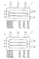
- FIG. 57 (a) shows a schematic bird's-eye view configuration of a conventional dual inline package 300a.
- FIG. 57 (b) shows a schematic bird's-eye view configuration of a conventional dual in-line package 300b that is simply reduced in size.
- the inter-terminal distance t1 in FIG. 57 (a) becomes t2 ( ⁇ t1) as shown in FIG. 57 (b), and the inter-terminal distance is reduced.
- An object of the present invention is to provide a power module semiconductor device that realizes a reduction in warpage due to a reduction in size of a transfer mold and a reduction in thermal stress, and a manufacturing method thereof.
- Two plate layers, a low-voltage side gate terminal electrode disposed on the first side of the ceramic substrate, and a low-voltage side source disposed on the first side and adjacent to the low-voltage side gate terminal electrode A terminal electrode, a high-voltage side gate terminal electrode disposed on the first side and spaced apart from the low-voltage side gate terminal electrode and the low-voltage side source terminal electrode, and disposed on the first side,
- the first plate layer on the surface of the ceramic substrate is patterned, and the low voltage side gate terminal electrode pattern, the low voltage side source terminal electrode pattern on the first side of the ceramic substrate, A high voltage side gate terminal electrode pattern and a high voltage side source terminal electrode pattern are formed, and a low voltage side drain electrode pattern, a high voltage side drain electrode pattern, and a ground electrode pattern are formed apart from the first side.
- An output terminal electrode is connected to the low-voltage side drain electrode pattern at a second side different from the first side, and the ground electrode pattern at a third side of the ceramic substrate different from the first side and the second side Connecting a ground electrode to the high-voltage side drain electrode pattern and connecting a power supply voltage supply terminal electrode to the high-voltage side drain electrode pattern; and the low-voltage side source terminal electrode
- the turn and the source pad electrode of the low-voltage side transistor are connected by a bonding wire
- the low-voltage side gate terminal electrode pattern and the gate pad electrode of the low-voltage side transistor are connected by a bonding wire
- the anode electrode of the low-voltage side diode is connected
- the step of dividing the ceramic substrate into a plurality of steps the step of forming the first plate layer on the surface of the divided ceramic substrate, and the back surface of the divided ceramic substrate.
- a step of mounting a high-voltage side diode connected in reverse parallel to the high-voltage side transistor, and connecting a low-voltage side gate terminal electrode to the low-voltage side gate terminal electrode pattern on the first side of the first ceramic substrate A low voltage side source terminal electrode is connected to the low voltage side source terminal electrode pattern, a high voltage side gate terminal electrode is connected to the high voltage side gate terminal electrode pattern, and a high voltage side source terminal electrode is connected to the high voltage side source terminal electrode pattern.
- the second ceramic substrate different from the first side of the first ceramic substrate, An output terminal electrode is connected to the low-voltage drain electrode pattern on the second side of the third ceramic substrate and the fourth ceramic substrate, and the first side is different from the first side and the second side.
- a ground potential terminal electrode is connected to the ground electrode pattern on a third side of the ceramic substrate, and the high-voltage side drain is connected to a third side of the fifth ceramic substrate different from the first side and the second side.
- a step of connecting a power supply voltage supply terminal electrode to the electrode pattern, a bonding wire connection between the low-voltage side source terminal electrode pattern and the source pad electrode of the low-voltage side transistor, and the low-voltage side gate terminal electrode pattern and the low-voltage side transistor The gate pad electrode of the high-voltage side source terminal electrode pattern and the high-voltage side transistor.
- the source pad electrode of the transistor is connected by a bonding wire, the high-voltage side gate terminal electrode pattern and the gate pad electrode of the high-voltage side transistor are connected by bonding wire, and the ground electrode pattern and the source pad of the low-voltage side transistor are connected.
- An electrode and the anode electrode of the low-voltage side diode are connected by stitch bonding, the source pad electrode of the high-voltage side transistor and the anode electrode of the high-voltage side diode are connected by a bonding wire, and the anode electrode of the high-voltage side diode.
- a step of dividing the ceramic substrate into a plurality of steps a step of forming a first plate layer on the surface of the ceramic substrate, and a second plate layer on the back surface of the ceramic substrate.
- Patterning the first plate layer to form a low voltage side gate terminal electrode pattern, a low voltage side source terminal electrode pattern, a high voltage side gate terminal electrode pattern, and a high voltage on the first side of the first ceramic substrate.
- a low-voltage side transistor and a low-voltage side diode connected in reverse parallel to the low-voltage side transistor are mounted on the low-voltage side drain electrode pattern, and reversely parallel to the high-voltage side transistor and the high-voltage side transistor on the high-voltage side drain electrode pattern Mounting a high voltage side diode to be connected; connecting a low voltage side gate terminal electrode to the low voltage side gate terminal electrode pattern on the first side of the first ceramic substrate; and connecting the low voltage side source terminal electrode pattern to the low voltage side source terminal electrode pattern A low voltage side source terminal electrode, a high voltage side gate terminal electrode connected to the high voltage side gate terminal electrode pattern, a high voltage side source terminal electrode connected to the high voltage side source terminal electrode pattern, and the first ceramic substrate On the second side of the fourth ceramic substrate different from the first side, the low-voltage side drain current An output terminal electrode is connected to the pattern, and a ground potential terminal electrode is connected to the ground electrode pattern at a third side of the first ceramic substrate and the second ceramic substrate different from the first side and the
- Terminal electrode pattern and the gate pad electrode of the high-voltage side transistor are connected by bonding wire, and the ground electrode pattern and the source pad electrode of the low-voltage side transistor and the anode electrode of the low-voltage side diode are connected by stitch bonding,
- Manufacturing a power module semiconductor device comprising: bonding a source pad electrode of a high-side transistor and an anode electrode of the high-voltage side diode by bonding wire connection, and connecting a bonding wire connection between the anode electrode of the high-voltage side diode and the low-voltage side drain electrode pattern A method is provided.
- the present invention it is possible to provide a power module semiconductor device that realizes a reduction in warpage due to a reduction in size of a transfer mold and a reduction in thermal stress, and a manufacturing method thereof.
- 4A is a schematic cross-sectional structure of a transfer mold resin taken along the line II in FIG. 4A, and FIG.
- FIG. 4A is a diagram corresponding to the case where there is no warpage, and FIG. Illustration.
- A The back surface block diagram of the power module semiconductor device which concerns on the modification 2 of 1st Embodiment, (b) The back surface block diagram of the power module semiconductor device which concerns on the modification 3 of 1st Embodiment.
- A The back surface block diagram of the power module semiconductor device which concerns on the modification 4 of 1st Embodiment,
- FIG. 6 is a plan structural view of a jig for injecting transfer mold resin in the power module semiconductor device according to the first modification of the first embodiment.
- A Schematic bird's-eye view configuration diagram of the power module semiconductor device according to the first embodiment,
- b Schematic when all of the terminal electrodes are bent in the power module semiconductor device according to the first embodiment.
- the typical plane pattern block diagram which shows the structure which mounted the terminal electrode of the power module semiconductor device which concerns on 1st Embodiment, a transistor, and a diode.
- the circuit block diagram of the power module semiconductor device which concerns on 1st Embodiment. (A) DBC substrate configuration example applicable to the power module semiconductor device according to the first embodiment, (b) Ceramic substrate configuration example applicable to the power module semiconductor device according to the first embodiment, (c) ) A schematic cross-sectional structure diagram for explaining one step of the method for manufacturing the power module semiconductor device according to the first embodiment (No. 1). Typical cross-section FIG. (2) explaining 1 process of the manufacturing method of the power module semiconductor device which concerns on 1st Embodiment. Typical cross-section FIG.
- FIG. 23 is a schematic plan pattern configuration diagram of the power module semiconductor device according to the first embodiment corresponding to the step of FIG. 22.
- Typical cross-section FIG. (6) explaining 1 process of the manufacturing method of the power module semiconductor device which concerns on 1st Embodiment.
- FIG. 3 is a schematic bird's-eye view configuration diagram illustrating how an electrolytic capacitor is connected between a power supply voltage supply terminal electrode PL and a ground potential terminal electrode NL in the power module semiconductor device according to the first embodiment.
- FIG. 3 is a circuit configuration diagram in which a capacitor C is connected between a power supply voltage supply terminal electrode PL and a ground potential terminal electrode NL in the power module semiconductor device according to the first embodiment.
- FIG. 4 is a schematic cross-sectional structure diagram of a SiC MOSFET that includes a source pad electrode SP and a gate pad electrode GP, which is an example of a semiconductor device applied to the power module semiconductor device according to the first embodiment.
- the typical bird's-eye view block diagram which shows the structure which mounted the terminal electrode, the transistor, and the diode in the power module semiconductor device which concerns on 2nd Embodiment.
- the typical plane pattern block diagram which shows the structure which mounted the terminal electrode, transistor, and diode of the power module semiconductor device which concerns on 2nd Embodiment.
- Typical cross-section FIG. (1) explaining 1 process of the manufacturing method of the power module semiconductor device which concerns on 2nd Embodiment.
- Typical cross-section FIG. (2) explaining 1 process of the manufacturing method of the power module semiconductor device which concerns on 2nd Embodiment.
- Typical cross-section FIG. (3) explaining 1 process of the manufacturing method of the power module semiconductor device which concerns on 2nd Embodiment.
- Typical cross-section FIG. (1) explaining 1 process of the manufacturing method of the power module semiconductor device which concerns on 2nd Embodiment.
- Typical cross-section FIG. (2) explaining 1 process of the manufacturing method of the power module semiconductor device which concerns on 2nd Embodiment.
- FIG. 45 is a schematic planar pattern configuration diagram of the power module semiconductor device according to the embodiment corresponding to the step of FIG. 44.
- A Schematic cross-sectional structure diagram for explaining one step of the method of manufacturing the power module semiconductor device according to the second embodiment (No. 7),
- B According to the second embodiment that is transfer-molded The typical cross-section figure of a power module semiconductor device.
- the typical bird's-eye view block diagram which shows the structure which mounted the terminal electrode, the transistor, and the diode in the power module semiconductor device which concerns on 3rd Embodiment.
- the typical plane pattern block diagram which shows the structure which mounted the terminal electrode, transistor, and diode of the power module semiconductor device which concerns on 3rd Embodiment.
- Typical cross-section FIG. (1) explaining 1 process of the manufacturing method of the power module semiconductor device which concerns on 3rd Embodiment.
- Typical cross-section FIG. (2) explaining 1 process of the manufacturing method of the power module semiconductor device which concerns on 3rd Embodiment.
- Typical cross-section FIG. (3) explaining 1 process of the manufacturing method of the power module semiconductor device which concerns on 3rd Embodiment.
- Typical cross-section FIG. (1) explaining 1 process of the manufacturing method of the power module semiconductor device which concerns on 3rd Embodiment.
- Typical cross-section FIG. (2) explaining 1 process of the manufacturing method of the power module semiconductor device which concerns on 3rd Embodi
- the typical plane pattern block diagram of the power module semiconductor device which concerns on embodiment corresponding to the process of FIG. (A) Schematic cross-sectional structure diagram for explaining one step of the method for manufacturing the power module semiconductor device according to the third embodiment (No. 7), (b) According to the third embodiment which is transfer-molded The typical cross-section figure of a power module semiconductor device.
- FIG. 1 A schematic external plan configuration of the power module semiconductor device 1 according to the first embodiment is expressed as shown in FIG. 1, and a back surface configuration is expressed as shown in FIG.
- the power module semiconductor device 1 includes a ceramic substrate 10, a first plate layer 10a, a second plate layer 10b, and a low-voltage side gate.
- the first plate layer 10a is disposed on the surface of the ceramic substrate 10, and the second plate layer 10b is disposed on the back surface of the ceramic substrate 10 and is divided into a plurality of parts.
- the second plate layer 10b is striped in the longitudinal direction of the ceramic substrate 10 (X direction in FIG. 12). It is divided.
- the first plate layer 10a and the second plate layer 10b can be formed of, for example, a copper plate layer.
- a DBC substrate as shown in FIG. 18A described later can be applied to the substrate structure composed of the ceramic substrate 10, the first plate layer 10a, and the second plate layer 10b. Or you may form by affixing the 1st plate layer 10a and the 2nd plate layer 10b suitably with respect to the surface and the back surface of the ceramic substrate 10.
- FIG. 18A A DBC substrate as shown in FIG. 18A described later can be applied to the substrate structure composed of the ceramic substrate 10, the first plate layer 10a, and the second plate layer 10b. Or you may form by affixing the 1st plate layer 10a and the 2nd plate layer 10b suitably with respect to the surface and the back surface of the ceramic substrate 10.
- the second plate layer 10b is divided into four rows. On the second plate layer 10b divided in this way, it is desirable that a heat source such as a transistor or a diode is disposed with the ceramic substrate 10 interposed therebetween in order to effectively perform heat dissipation.
- a heat source such as a transistor or a diode
- the low-voltage side gate terminal electrodes GL4, GL5, and GL6 are arranged on the first side of the ceramic substrate.
- the low-voltage side source terminal electrodes SL4, SL5, and SL6 are arranged on the first side and are arranged adjacent to the low-voltage side gate terminal electrodes GL4, GL5, and GL6, respectively.
- the high-voltage side gate terminal electrodes GL1, GL2, and GL3 are arranged on the first side, and are separated from the low-voltage side gate terminal electrodes GL4, GL5, and GL6 and the low-voltage side source terminal electrodes SL4, SL5, and SL6.
- the high-voltage side source terminal electrodes SL1, SL2, and SL3 are arranged on the first side and are arranged adjacent to the high-voltage side gate terminal electrodes GL1, GL2, and GL3, respectively.
- the output terminal electrodes UL, VL, WL are arranged on the second side opposite to the first side of the ceramic substrate.
- the power supply voltage supply terminal electrode PL is arranged on a third side of the ceramic substrate different from the first side and the second side.
- the ground potential terminal electrode NL is disposed on the third side and is spaced apart from the power supply voltage supply terminal electrode PL.
- the ceramic substrate 10 can be formed of any one of aluminum oxide (Al 2 O 3 ), aluminum nitride (AlN), and silicon nitride (SiN).
- the ceramic substrate 10 / first plate layer 10a and second plate layer 10b can be formed of any one of an aluminum oxide substrate / Cu plate electrode, an aluminum nitride substrate / Al plate electrode, and a silicon nitride substrate / Cu plate electrode. .
- Examples of the combination of the ceramic substrate 10 / second plate layer 10b functioning as a heat sink include an alumina substrate / Cu plate electrode, an aluminum nitride substrate / Al plate electrode, a silicon nitride substrate / Cu plate electrode, and the like. .
- the aluminum nitride substrate is characterized by low thermal resistance.
- the thermal resistance of the silicon nitride substrate is about 1/3 that of the aluminum nitride substrate, and the high temperature characteristics are also good.
- the combination of the alumina substrate / Cu plate electrode is the cheapest.
- the back surface configuration of the power module semiconductor device according to the comparative example is expressed as shown in FIG.
- the second plate layer 10b functioning as a heat sink is formed as a uniform plate electrode layer.
- the second plate layer 10b functioning as a heat sink is divided into a plurality of parts.
- the simulation result showing the warpage state of the power module semiconductor device according to the comparative example is expressed as shown in FIG. 4A
- the simulation result showing the warpage state of the power module semiconductor device according to the first embodiment is It is expressed as shown in FIG. 4A
- FIG. 4A a schematic cross-sectional structure of the transfer mold resin taken along the line II in FIG. 4A and corresponding to the case where there is no warpage is expressed as shown in FIG.
- An explanatory diagram of the warp amount D corresponding to a certain case is expressed as shown in FIG.
- the maximum displacement amount of the warp amount D is minus 0.528 mm.
- the maximum displacement amount of the warp amount D is minus 0.281 mm. .
- the module when a module is produced by transfer molding, the module functions as a heat sink in order to suppress deformation of the module due to thermal stress in a high temperature environment.
- the stress and the deformation amount of the module can be reduced.
- a groove is formed in the second plate layer 10b functioning as a heat sink so that the resin is wound on both the front and back surfaces of the transfer mold module.
- the inter-terminal distance L4 between the low-voltage side source terminal electrode SL6 and the high-voltage side gate terminal electrode GL1 is, for example, about 6 mm, and between the high-voltage side source terminal electrode SL1 and the high-voltage side gate terminal electrode GL2.
- the inter-terminal distance L5 is about 6 mm, for example, and the inter-terminal distance L6 between the high-voltage side source terminal electrode SL2 and the high-voltage side gate terminal electrode GL3 is about 6 mm, for example.
- the inter-terminal distance L1 between the output terminal electrode UL and the output terminal electrode VL is, for example, about 6 mm
- the inter-terminal distance L2 between the output terminal electrode VL and the output terminal electrode WL is, for example, about 6 mm
- the inter-terminal distance L3 between the power supply voltage supply terminal electrode PL and the ground potential terminal electrode NL is, for example, about 6 mm.
- the distance between the terminals along the edge of the ceramic substrate between the high-voltage side source terminal electrode SL3 and the ground potential terminal electrode NL is, for example, about 6 mm.
- the inter-terminal distance along the edge of the ceramic substrate between the output terminal electrode WL and the power supply voltage supply terminal electrode PL is, for example, about 6 mm. Furthermore, the distance between the terminal electrodes GL4, SL4, GL5, SL5, GL6, and SL6 is, for example, about 1 mm. Similarly, the distance between the terminal electrodes GL1 and SL1, the distance between the terminal electrodes GL2 and SL2, and the distance between the terminal electrodes GL3 and SL3 are about 1 mm, for example.
- the inter-terminal distances L1 and L2 are preferably longer than the inter-terminal distances L4 and L5.
- the width W1 of the ceramic substrate 10 covered with the transfer mold resin 12 is, for example, about 6 mm or more.
- the transfer mold resin 12 is also formed between the divided second plate layers 10b.
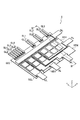
- FIG. 12A a schematic bird's-eye view configuration along the XYZ-axis direction of the power module semiconductor device 1 according to the first embodiment is expressed as shown in FIG. 12A and is a schematic view when all of the terminal electrodes are bent.
- the bird's-eye view configuration is expressed as shown in FIG. 12A
- the length L in the X-axis direction of the transfer mold resin 12 is, for example, about 48 mm
- the width W in the Y-axis direction is, for example, about 32 mm
- the thickness in the Z-axis direction is, for example, about 3.5 mm.
- the thickness of the ceramic substrate 10 is, for example, about 0.35 to 0.68 mm.
- the thickness of about 3.5 mm in the Z-axis direction is the dimension of the entire thickness of the transfer mold resin 12 molded on the front and back surfaces of the ceramic substrate 10 (see FIG. 26A).
- the thickness is, for example, about 29 mm.
- a transfer mold module is formed in order to reduce the size.
- the terminal electrode can be taken out from the three directions of the mold package to obtain an insulation distance.
- the high voltage side signal terminal is arranged away from the low voltage side signal terminal, and the low voltage side signal terminal is arranged in part.
- the low voltage side signal terminals are arranged side by side, the high voltage side signal terminals are arranged apart from each other, the output terminals are arranged apart from the low voltage side and high voltage side signal terminals, and the power supply voltage
- the terminal and the ground potential terminal are arranged separately from the output terminal and the signal terminal.
- the power supply voltage terminal, the ground potential terminal, the low-voltage side and the high-voltage side signal terminal and the output terminal are taken out from the three directions of the module package of the transfer mold to increase the insulation distance. It can also be taken.
- the power supply voltage supply terminal electrode PL and the ground potential terminal electrode NL are disposed adjacent to each other in order to facilitate the connection between the power supply V and the capacitor C. .
- the widths of the output terminal electrodes UL, VL, and WL may be set wide in a portion where strain stress is applied when the resin of the transfer mold resin is injected. That is, in the power module semiconductor device 1 according to the first embodiment, a resin injection gate is formed on the power terminal side of the high heat resistant mold module, and a protrusion for preventing slippage is provided on the power terminal of the high heat resistant mold module. It may be produced.
- the high heat-resistant resin is somewhat hard, and a thin signal wire bonding wire may come off during resin injection molding. Since the power bonding wire on the power terminal side is thicker than the signal wire bonding wire, it is desirable to inject the resin of the high heat-resistant resin from the power terminal side.
- the diameter of the bonding wire for signal lines is, for example, about 150 ⁇ m
- the diameter of the bonding wire for power is, for example, about 350 ⁇ m.
- the convex part is formed in the power terminal.
- the convex portion By forming the convex portion inside the power terminal, it is possible to increase the strength of the power terminal and to prevent the power bonding wire from coming off. That is, since the heat-resistant resin having a relatively high hardness is injected from the side resistant to stress during resin injection molding, defects during assembly can be reduced.
- the first embodiment it is possible to provide a power module semiconductor device that realizes a reduction in warpage by reducing the size of a transfer mold and reducing thermal stress.
- the power module semiconductor device 1 includes a plurality of second plate layers 10b whose corner portions are processed into a tapered shape. This is because the transfer mold resin 12 is effectively injected between the divided second plate layers 10b in the transfer mold resin 12 injection step.
- the width W1 of the ceramic substrate 10 covered with the transfer mold resin 12 is, for example, about 6 mm or more.
- the transfer mold resin 12 is also formed between the divided second plate layers 10b.
- Other configurations are the same as those of the first embodiment.
- a jig 400 for injecting the transfer mold resin 12 includes a conduction hole 420 of the transfer mold resin 12, as shown in FIG.
- the cavity 500 is connected to the conduction hole 420 and into which the transfer mold resin 12 is injected.
- the jig 400 is formed of a metal block that can be divided vertically.
- FIG. 11 shows a planar configuration of the lower metal block.
- the upper metal block is combined with the lower metal block so that only the conduction hole 420 and the cavity 500 become a cavity.
- the transfer mold resin 12 is divided in the transfer mold resin 12 injection step. Further, it can be effectively injected also between the second plate layers 10b.
- the first modification of the first embodiment it is possible to provide a power module semiconductor device that realizes a reduction in warpage due to downsizing of a transfer mold and reduction of thermal stress.
- the second plate layer 10b is divided into stripes in three rows in the longitudinal direction of the ceramic substrate 10.
- a heat source such as a transistor or a diode is disposed with the ceramic substrate 10 interposed therebetween in order to effectively perform heat dissipation.
- the power module semiconductor device 1 according to Modification 3 of the first embodiment includes a plurality of second plate layers 10b in which corner portions are processed into a tapered shape, as illustrated in FIG.
- the transfer mold resin 12 can be effectively injected also between the divided second plate layers 10b.
- the width W1 of the ceramic substrate 10 covered with the transfer mold resin 12 is, for example, about 6 mm or more.
- the transfer mold resin 12 is also formed between the divided second plate layers 10b.
- Other configurations are the same as those of the first embodiment.
- Modifications 2 and 3 of the first embodiment it is possible to provide a power module semiconductor device that realizes reduction in warpage due to downsizing of the transfer mold and reduction of thermal stress.
- the second plate layer 10b is divided into island shapes.
- the second plate layer 10b is divided into 3 ⁇ 6 islands.
- a heat source such as a transistor or a diode is disposed with the ceramic substrate 10 interposed therebetween in order to effectively perform heat dissipation.
- the power module semiconductor device 1 according to the modification 5 of the first embodiment includes a plurality of second plate layers 10b in which corner portions are processed into a tapered shape as illustrated in FIG.
- the transfer mold resin 12 can be effectively injected also between the divided second plate layers 10b.
- the width W1 of the ceramic substrate 10 covered with the transfer mold resin 12 is, for example, about 6 mm or more.
- the transfer mold resin 12 is also formed between the divided second plate layers 10b.
- Other configurations are the same as those of the first embodiment.
- Modifications 4 and 5 of the first embodiment it is possible to provide a power module semiconductor device that realizes a reduction in warpage due to downsizing of the transfer mold and reduction of thermal stress.
- Modifications 6 and 7 The back surface configuration of the power module semiconductor device according to Modification 6 of the first embodiment is represented as shown in FIG. 8A, and the back surface configuration of the power module semiconductor device according to Modification 7 is illustrated in FIG. It is expressed as shown in b).
- the second plate layer 10b is divided into 3 ⁇ 4 islands.
- a heat source such as a transistor or a diode is disposed with the ceramic substrate 10 interposed therebetween in order to effectively perform heat dissipation.
- the power module semiconductor device 1 according to the modified example 7 of the first embodiment includes a plurality of second plate layers 10b in which the corner portion is processed into a curved surface shape as illustrated in FIG.
- the transfer mold resin 12 can be effectively injected also between the divided second plate layers 10b.
- the width W1 of the ceramic substrate 10 covered with the transfer mold resin 12 is, for example, about 6 mm or more.
- the transfer mold resin 12 is also formed between the divided second plate layers 10b.
- Other configurations are the same as those of the first embodiment.
- Modifications 6 and 7 of the first embodiment it is possible to provide a power module semiconductor device that realizes a reduction in warpage due to downsizing of the transfer mold and reduction of thermal stress.
- the island-like structure of the second plate layer 10b of the modified examples 4 and 5 or modified examples 6 and 7 can be selected as appropriate.
- the second plate layer 10b is divided into stripes in six rows in the short direction of the ceramic substrate 10.
- a heat source such as a transistor or a diode is disposed with the ceramic substrate 10 interposed therebetween in order to effectively perform heat dissipation.
- the power module semiconductor device 1 according to the modification 9 of the first embodiment includes a plurality of second plate layers 10b whose corner portions are processed into curved surfaces as shown in FIG. 9B, In the step of injecting the transfer mold resin 12, the transfer mold resin 12 can be effectively injected also between the divided second plate layers 10b.
- the width W1 of the ceramic substrate 10 covered with the transfer mold resin 12 is, for example, about 6 mm or more.
- the transfer mold resin 12 is also formed between the divided second plate layers 10b.
- Other configurations are the same as those of the first embodiment.
- Modifications 8 and 9 of the first embodiment it is possible to provide a power module semiconductor device that realizes a reduction in warpage due to downsizing of the transfer mold and reduction of thermal stress.
- Modifications 10 and 11 The back surface configuration of the power module semiconductor device according to Modification Example 10 of the first embodiment is represented as shown in FIG. 10A, and the back surface configuration of the power module semiconductor device according to Modification Example 11 is illustrated in FIG. It is expressed as shown in b).
- the second plate layer 10b is divided into four rows in the lateral direction of the ceramic substrate 10 in a stripe shape.
- a heat source such as a transistor or a diode is disposed with the ceramic substrate 10 interposed therebetween in order to effectively perform heat dissipation.
- the power module semiconductor device 1 according to the eleventh modification of the first embodiment includes a plurality of second plate layers 10b in which corner portions are processed into curved surfaces, as illustrated in FIG.
- the transfer mold resin 12 can be effectively injected also between the divided second plate layers 10b.
- the width W1 of the ceramic substrate 10 covered with the transfer mold resin 12 is, for example, about 6 mm or more.
- the transfer mold resin 12 is also formed between the divided second plate layers 10b.
- Other configurations are the same as those of the first embodiment.
- the island-like structure of the second plate layer 10b of the modified examples 8 and 9 or the modified examples 10 and 11 can be appropriately selected. is there.
- the terminal electrode may be bent in the height direction of the substrate when the power module semiconductor device 1 is mounted on the mounting substrate 200.
- FIG. 13 is a diagram for explaining a variation of bending of the gate terminal electrode GL in the power module semiconductor device 1 according to the first embodiment.
- FIG. 13A illustrates the case where the bending process is not performed
- FIG. 13B illustrates the case where the bending process GLs is performed at the substantially central portion of the gate terminal electrode GL. If such a U-shaped bending process GLs is performed, the stress can be absorbed even when the gate terminal electrode GL receives some load.
- FIG. 13 (c) shows a case in which the bending is gently inclined to the left side in the drawing
- FIG. 13 (d) shows a case in which a bending operation GLk that is inclined sharply to the left in the drawing is applied. Is illustrated.
- FIG. 13D is more than FIG. 13C. Can bring the tip GLt of the gate terminal electrode GL closer to the power module semiconductor device 1 side.
- the power module semiconductor device 1 according to the first embodiment is covered by the transfer mold resin 12 and is therefore denoted by reference numeral 12. Yes.
- the power module semiconductor device 1 according to the first embodiment is mounted on the mounting substrate 200 via the adhesive 13.
- the adhesive 13 may be a conductive adhesive or a solder layer. 13 (a) to 13 (d), the variation of the bending process of the gate terminal electrode GL has been described.
- the gate terminal electrode GL includes the gate terminal electrodes GL1, GL2,. It corresponds to GL3, GL4, GL5, and GL6. 13 (a) to 13 (d), the variation of the bending process of the gate terminal electrode GL has been described. However, other source terminal electrodes SL1, SL2, SL3, SL4, SL5, SL6, output terminal electrodes The same applies to UL / VL / WL, ground potential terminal electrode NL, power supply voltage supply terminal electrode PL, and the like.
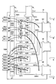
- FIG. 15 a schematic bird's-eye view configuration showing a structure in which terminal electrodes, transistors, and diodes are mounted is expressed as shown in FIG. An enlarged view of is shown as shown in FIG.
- the low-voltage side transistor Q4 is disposed on the low-voltage side drain electrode pattern D (K4), and the gate pad electrode GP4 of the low-voltage side transistor Q4 is surrounded by the source pad electrode SP4. Are arranged.
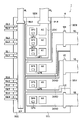
- FIG. 1 a schematic planar pattern configuration showing a structure in which the terminal electrodes, transistors, and diodes of the power module semiconductor device 1 according to the first embodiment are mounted is expressed as shown in FIG.
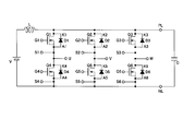
- the circuit configuration of the power module semiconductor device 1 according to the embodiment is expressed as shown in FIG.
- the first plate layer 10a includes the low-voltage side gate terminal electrode patterns GLP4, GLP5, and GLP6, and the low-voltage side source terminal electrode.
- Low voltage side drain electrode pattern on which patterns SLP4, SLP5, SLP6, high voltage side gate terminal electrode patterns GLP1, GLP2, GLP3, high voltage side source terminal electrode patterns SLP1, SLP2, SLP3 and low voltage side transistors Q4, Q5, Q6 are mounted D (K4), D (K5), D (K6), a high-voltage drain electrode pattern D (K) on which the high-voltage transistors Q1, Q2, Q3 are mounted, and a ground electrode pattern EP.
- the low-voltage side drain electrode patterns D (K4), D (K5), and D (K6) have a low voltage.
- Low-voltage side diodes D4, D5, and D6 connected in reverse parallel to the side transistors Q4, Q5, and Q6 are mounted, and the high-voltage side drain electrode pattern D (K) is connected in reverse parallel to the high-voltage side transistors Q1, Q2, and Q3.
- High-voltage side diodes D1, D2, and D3 are mounted.
- At least the low-voltage side drain electrode pattern D (K4) / D (K5) / D (K6) or the high-voltage side drain electrode pattern D (K) is divided into a plurality.
- the second plate layer 10b is preferably opposed to the ceramic substrate 10 in order to effectively dissipate heat.
- the ground electrode pattern EP and the second plate layer 10b divided into a plurality are also opposed to each other with the ceramic substrate 10 interposed therebetween to dissipate heat. Desirable for effective implementation.
- the chip size of the transistors Q1, Q2, Q3, Q4, Q5, and Q6 is, for example, about 5 mm ⁇ 5 mm, and the thickness is, for example, about 0.25 mm.
- the chip size of the diodes D1, D2, D3, D4, D5, and D6 is, for example, about 5 mm ⁇ 5 mm, and the thickness is, for example, about 0.25 mm.
- the chip size is not limited to this, and may be, for example, 4 mm square to 6 mm square.
- the thickness of the ground electrode pattern EP is, for example, about 0.3 to 0.4 mm.
- the thickness of each terminal electrode is about 0.2 mm, for example.
- the thickness of the solder layers 14 and 15 is, for example, about 0.1 mm.
- the power module semiconductor device 1 includes first bonding wires SW4, SW5, and SW6, and second bonding wires GW4, GW5, and GW6 as shown in FIGS. , Third bonding wires SW1, SW2, and SW3, fourth bonding wires GW1, GW2, and GW3, fifth bonding wires AW4, AW5, and AW6, sixth bonding wires AW1, AW2, and AW3, and seventh bonding wires BW1 -BW2 and BW3 are provided.
- first bonding wires SW4, SW5, and SW6 connect the low-voltage side source terminal electrode patterns SLP4, SLP5, and SLP6 to the source pad electrodes SP4, SP5, and SP6 of the low-voltage side transistors Q4, Q5, and Q6.
- the second bonding wires GW4, GW5, and GW6 connect the low-voltage side gate terminal electrode patterns GLP4, GLP5, and GLP6 to the gate pad electrodes GP4, GP5, and GP6 of the low-voltage side transistors Q4, Q5, and Q6.
- the third bonding wires SW1, SW2, and SW3 connect the high-voltage side source terminal electrode patterns SLP1, SLP2, and SLP3 to the source pad electrodes SP1, SP2, and SP3 of the high-voltage side transistors Q1, Q2, and Q3.
- the fourth bonding wires GW1, GW2, and GW3 connect the high-voltage side gate terminal electrode patterns GLP1, GLP2, and GLP3 to the gate pad electrodes GP1, GP2, and GP3 of the high-voltage side transistors Q1, Q2, and Q3.
- the fifth bonding wires AW4, AW5, and AW6 include the ground electrode pattern EP, the source pad electrodes SP4, SP5, and SP6 of the low-voltage side transistors Q4, Q5, and Q6, and the anode electrodes A4, A5, and A6 of the low-voltage side diodes D4, D5, and D6. And the stitch bonding connection.
- the sixth bonding wires AW1, AW2, and AW3 connect the source pad electrodes SP1, SP2, and SP3 of the high-voltage side transistors Q1, Q2, and Q3 to the anode electrodes A1, A2, and A3 of the high-voltage side diodes D1, D2, and D3.
- the seventh bonding wires BW1, BW2, and BW3 connect the anode electrodes A1, A2, and A3 of the high-voltage side diodes D1, D2, and D3 to the low-voltage side drain electrode patterns D (K4), D (K5), and D (K6).
- the sixth bonding wires AW1, AW2, and AW3 and the seventh bonding wires BW1, BW2, and BW3 may be stitch-bonded.
- the low-voltage side gate terminal electrode patterns GLP4, GLP5, and GLP6 are equipped with low-voltage side gate terminal electrodes GL4, GL5, and GL6, and the low-voltage side source terminal electrode patterns SLP4, SLP5, and Low-voltage side source terminal electrodes SL4, SL5, and SL6 are mounted on SLP6, and high-voltage side gate terminal electrodes GL1, GL2, and GL3 are mounted on high-voltage side gate terminal electrode patterns GLP1, GLP2, and GLP3.
- the electrode patterns SLP1, SLP2, and SLP3 have high-voltage side source terminal electrodes SL1, SL2, and SL3 mounted thereon, the ground electrode pattern EP has a ground potential terminal electrode NL mounted thereon, and the high-voltage side drain electrode pattern D (K). Is provided with a power supply voltage supply terminal electrode PL and a low-voltage drain electrode pattern D (K ) The ⁇ D (K5) ⁇ D (K6), the output terminal electrode UL ⁇ VL ⁇ WL is mounted.
- the output terminal electrodes UL, VL, and WL include output terminal electrode expansion portions UE, VE, and WE for increasing the strength. May be.
- the power supply voltage supply terminal electrode PL and the ground potential terminal electrode NL have power supply voltage supply terminal electrodes for increasing the strength, as shown in FIG.
- the extended portion PLE and the ground potential terminal electrode extended portion NLE may be provided.
- the electrode expansion portions for increasing the strength include the high-voltage side gate terminal electrodes GL1, GL2, and GL3, the high-voltage side source terminal electrodes SL1, SL2, and SL3, and the low-voltage side gate terminal electrode GL4. -You may form in each connection part of GL5 * GL6 and low voltage
- the front and back surfaces of the ceramic substrate 10 are formed.
- the transfer mold resin 12 is provided except on the second plate layer 10b.
- FIGS. 18 to 22, FIG. 24, and FIG. A schematic planar pattern configuration of the power module semiconductor device 1 according to the first embodiment corresponding to the step of FIG. 22 is represented as shown in FIG. 23, and the first embodiment corresponding to the step of FIG.
- a schematic planar pattern configuration of the power module semiconductor device 1 according to the embodiment is expressed as shown in FIG.
- the substrate structure of the power module semiconductor device 1 according to the first embodiment is applicable to a DBC substrate composed of a ceramic substrate 10, a first plate layer 10a, and a second plate layer 10b as shown in FIG. is there. Or you may form by affixing the 1st plate layer 10a and the 2nd plate layer 10b suitably on the surface and the back surface of the ceramic substrate 10 as shown in FIG.18 (b).
- the first plate layer 10a and the second plate layer 10b can be formed of, for example, a copper plate layer.
- the second plate layer 10b on the back surface of the ceramic substrate 10 is patterned and divided into a plurality of parts.
- the first plate layer 10 a on the surface of the ceramic substrate 10 is patterned to form the first of the ceramic substrate 10.
- SLP2 and SLP3 are formed and separated from the first side by a low-voltage side drain electrode pattern D (K4) / D (K5) / D (K6), a high-voltage side drain electrode pattern D (K), and a ground Forming an electrode pattern EP.
- the method for manufacturing the power module semiconductor device 1 according to the first embodiment includes the low voltage side on the low voltage side drain electrode patterns D (K4), D (K5), and D (K6).
- the low-voltage side diodes D4, D5, and D6 connected in reverse parallel to the transistors Q4, Q5, and Q6 and the low-voltage side transistors Q4, Q5, and Q6 are mounted, and the high-voltage side transistors Q1 and Q2 are mounted on the high-voltage side drain electrode pattern D (K).
- the low-voltage side gate terminal electrode patterns GLP4, GLP5, and GLP6 have a low-voltage side on the first side of the ceramic substrate 10.
- the gate terminal electrodes GL4, GL5, GL6 are connected, the low voltage side source terminal electrode patterns SLP4, SLP5, SLP6 are connected to the low voltage side source terminal electrodes SL4, SL5, SL6, and the high voltage side gate terminal electrode patterns GLP1, GLP2, GLP3 are connected.
- the high-voltage side gate terminal electrodes GL1, GL2, and GL3 are connected, and the high-voltage side source terminal electrode patterns SLP1, SLP2, and SLP3 are connected to the high-voltage side source terminal electrodes SL1, SL2, and SL3, and separated from the first side of the ceramic substrate 10
- the output terminal electrodes UL, VL, WL are connected to D (K6), and the ground potential terminal electrode NL is connected to the ground electrode pattern EP on the third side of the ceramic substrate 10 different from the first side and the second side.
- the method for manufacturing the power module semiconductor device 1 according to the first embodiment includes the low-voltage side source terminal electrode patterns SLP4, SLP5, and SLP6 and the low-voltage side transistors Q4, Q5, and Q6.
- Source pad electrodes SP4, SP5, and SP6 are connected using bonding wires SW4, SW5, and SW6, and the low-voltage side gate terminal electrode patterns GLP4, GLP5, and GLP6 are connected to the gate pad electrodes GP4 and GP4 of the low-voltage side transistors Q4, Q5, and Q6.
- GP5 and GP6 are connected using bonding wires GW4, GW5, and GW6, and the high-voltage side source terminal electrode patterns SLP1, SLP2, and SLP3 are bonded to the source pad electrodes SP1, SP2, and SP3 of the high-voltage side transistors Q1, Q2, and Q3.
- the high-voltage side gate terminal electrode patterns GLP1, GLP2, and GLP3 and the gate pad electrodes GP1, GP2, and GP3 of the high-voltage side transistors Q1, Q2, and Q3 are connected using bonding wires GW1, GW2, and GW3, and ground electrodes
- the pattern EP and the source pad electrodes SP4, SP5, and SP6 of the low-voltage side transistors Q4, Q5, and Q6 and the anode electrodes A4, A5, and A6 of the low-voltage side diodes D4, D5, and D6 are stitched using bonding wires AW4, AW5, and AW6.
- Bonding connection is made, and source pad electrodes SP1, SP2, and SP3 of high-voltage side transistors Q1, Q2, and Q3 and anode electrodes A1, A2, and A3 of high-voltage side diodes D1, D2, and D3 are bonded using bonding wires AW1, AW2, and AW3.
- bonding wires AW1, AW2, and AW3 Connect the high-voltage diode D ⁇ D2 ⁇ D3 of the anode electrode A1 ⁇ A2 ⁇ A3 and the low pressure side drain electrode pattern D (K4) ⁇ D (K5) ⁇ D (K6) and using a bonding wire BW1 ⁇ BW2 ⁇ BW3 a has the step of connecting.
- bonding wires SW1, SW2, SW3, SW4, SW5, SW6 and bonding wires GW1, GW2, GW3, GW4, GW5, and GW6 use relatively thin bonding wires.
- Bonding wires AW1, AW2, AW3, AW4, AW5, and AW6 and bonding wires BW1, BW2, and BW3 use relatively thick bonding wires. Although shown as one in the drawing, for example, about four relatively thick bonding wires may be connected in parallel.
- the relatively thick bonding wire connection before the relatively thin bonding wire connection. Further, it is desirable to perform the bonding wire connection between the transistors Q1, Q2, Q3, Q4, Q5, and Q6 and the diodes D1, D2, D3, D4, D5, and D6 before the bonding wire connection of the terminal electrode pattern. . This is to prevent the relatively thin bonding wire from being damaged by the force applied when the relatively thick bonding wire is connected.
- the low-voltage drain electrode patterns D (K4) and D (K5) are shown by the arrow B in FIGS. 24 and 25, the low-voltage drain electrode patterns D (K4) and D (K5) ).
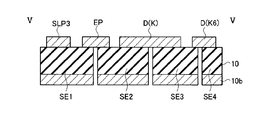
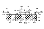
- FIGS. 18 (c) to 22, 24, 26 (a) and 26 (b) show a schematic cross-sectional structure taken along line II-II in FIG.
- a DBC substrate having a first plate layer 10 a on the surface of the ceramic substrate 10 and a second plate layer 10 b on the back surface of the ceramic substrate 10 is prepared.
- the first plate layer 10a is formed on the surface of the ceramic substrate 10 having a schematic cross-sectional structure as shown in FIG. 18B
- the second plate layer 10b is formed on the back surface of the ceramic substrate 10. You may form by doing.
- the 2nd plate layer 10b is patterned and the 2nd plate layer 10b is divided
- transistors Q1 to Q6, diodes D1 to D6, and the like are disposed on the divided second plate layer 10b with the ceramic substrate 10 interposed therebetween. This is to effectively carry out heat radiation from the transistors Q1 to Q6 and the diodes D1 to D6.
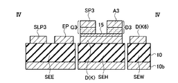
- the first plate layer 10a is patterned to form a high-voltage side source terminal electrode pattern SLP3, a ground electrode pattern EP, a high-voltage side drain electrode pattern D (K), and a low-voltage side drain electrode.
- a pattern D (K6) is formed.
- the high voltage side transistor Q1 and the high voltage side diode D3 are mounted on the high voltage side drain electrode pattern D (K) via the solder layer 15.
- the high voltage side transistor Q1 and the high voltage side diode D3 are connected in reverse parallel to each other, and the high voltage side drain electrode pattern D (K) is connected to the drain electrode of the high voltage side transistor Q1 and the cathode electrode of the high voltage side diode D3.
- the high voltage side source terminal electrode SL3 is connected to the high voltage side source terminal electrode pattern SLP3 via the solder layer 14, and the low voltage side drain electrode pattern D (K6) is formed.
- the output terminal electrode WL is connected through the solder layer 16.
- the high-voltage side source terminal electrode pattern SLP3 and the source pad electrode SP3 of the high-voltage side transistor Q3 are connected using the bonding wire SW3, and the source pad electrode SP3 of the high-voltage side transistor Q3 is connected.
- the anode electrode A3 of the high-voltage side diode D3 are connected using a bonding wire AW3, and the anode electrode A3 of the high-voltage side diode D3 and the low-voltage side drain electrode pattern D (K6) are connected using a bonding wire BW3.
- the low-voltage source terminal electrode patterns SLP4, SLP5, and SLP6 and the source pad electrodes SP4, SP5, and SP6 of the low-voltage transistors Q4, Q5, and Q6 are bonded to the bonding wires SW4 and SW5. -Connect using SW6.
- the low-voltage side gate terminal electrode patterns GLP4, GLP5, and GLP6 are connected to the gate pad electrodes GP4, GP5, and GP6 of the low-voltage side transistors Q4, Q5, and Q6 using bonding wires GW4, GW5, and GW6.
- the high-voltage side source terminal electrode patterns SLP1, SLP2, and SLP3 are connected to the source pad electrodes SP1, SP2, and SP3 of the high-voltage side transistors Q1, Q2, and Q3 using bonding wires SW1, SW2, and SW3.
- the high-voltage side gate terminal electrode patterns GLP1, GLP2, and GLP3 and the gate pad electrodes GP1, GP2, and GP3 of the high-voltage side transistors Q1, Q2, and Q3 are connected using bonding wires GW1, GW2, and GW3.
- ground electrode pattern EP and the source pad electrodes SP4, SP5, and SP6 of the low-voltage side transistors Q4, Q5, and Q6 and the anode electrodes A4, A5, and A6 of the low-voltage side diodes D4, D5, and D6 are bonded to the bonding wires AW4, AW5, and AW6. Connect with stitch bonding.
- the source pad electrodes SP1, SP2, and SP3 of the high-voltage side transistors Q1, Q2, and Q3 and the anode electrodes A1, A2, and A3 of the high-voltage side diodes D1, D2, and D3 are bonded using bonding wires AW1, AW2, and AW3.
- the anode electrodes A1, A2, and A3 of the high-voltage side diodes D1, D2, and D3 and the low-voltage side drain electrode patterns D (K4), D (K5), and D (K6) are stitch-bonded using bonding wires BW1, BW2, and BW3. Connecting.
- bonding wire AW1 and the bonding wire BW1 may be stitch-bonded continuously with one bonding wire.
- bonding wire AW2 and bonding wire BW2 may be stitch-bonded continuously with one bonding wire.
- bonding wire AW3 and bonding wire BW3 may be stitch-bonded continuously with one bonding wire.
- the portion indicated by the bonding wire AW4 is different between the ground electrode pattern EP and the source pad electrode SP4 of the low voltage side transistor Q4, and between the source pad electrode SP4 of the low voltage side transistor Q4 and the anode electrode A4 of the low voltage side diode D4.
- Wire bonding connection may be performed using a bonding wire. The same applies to the bonding wire AW5 and the bonding wire AW6.
- the transfer mold resin 12 is formed from the side of the ceramic substrate 10 on which the low-voltage side drain electrode patterns D (K4), D (K5), and D (K6) are formed. Inject.
- a material of the transfer mold resin 12 for example, a thermosetting epoxy resin can be applied.
- gate bonding wires (thin wire wires) GW4, GW5, and GW4 that connect the low-voltage side gate terminal electrode patterns GLP4, GLP5, and GLP6 of the ceramic substrate 10 to the gate pad electrodes GP4, GP5, and GP6 of the low-voltage side transistors Q4, Q5, and Q6.
- the transfer mold resin 12 may be injected from the direction facing the GW 6.
- the transfer mold resin 12 is formed on the front surface and the back surface of the ceramic substrate 10.
- the transfer mold resin 12 is formed so as to cover the front surface and the back surface of the ceramic substrate 10 except on the second plate layer 10b. That is, the transfer mold resin 12 is also formed on the back surface of the ceramic substrate 10 in the groove between the divided second plate layers 10b.
- the power module semiconductor device 1 according to the first embodiment shown in FIGS. 1A and 12A is completed.
- the peripheral part of the transfer mold resin 12 it is desirable for the peripheral part of the transfer mold resin 12 to have angle (theta).
- the value of the angle ⁇ is, for example, about 70 to 85 degrees.
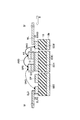
- FIG. 27A a schematic planar pattern configuration in the vicinity of the output terminal electrode WL is expressed as shown in FIG. 27A, and is taken along the line III-III in FIG.
- a schematic cross-sectional structure along the line is represented as shown in FIG.
- the output terminal electrode WL includes an output terminal electrode extension WE, thereby providing a low-voltage side drain electrode pattern D (K6). ) And the output terminal electrode WL can be increased. For this reason, disconnection between the output terminal electrode WL and the low-voltage side drain electrode pattern D (K6) can be prevented, and the connection reliability can be improved.
- the dimensions EW1 and EW2 of the expanded portion of the output terminal electrode extended portion WE are, for example, about 20% of the width of the output terminal electrode WL.
- a schematic bird's-eye view configuration for explaining a state in which the electrolytic capacitor 20 is connected between the power supply voltage supply terminal electrode PL and the ground potential terminal electrode NL is as shown in FIG. It is expressed in
- the power supply voltage supply terminal electrode PL and the ground potential terminal electrode NL may include pinholes 18P and 18N for connecting the pins 22P and 22N of the electrolytic capacitor 20, as shown in FIG. In addition, you may provide the screw hole instead of the pinhole 18P * 18N.
- the SiC MOSFET can be miniaturized and can conduct a large current. In SiMOSFETs and Si-based IGBTs, the allowable power amount has been limited to 10 W / cc, but in the power module semiconductor device 1 according to the first embodiment equipped with a SiC-based MOSFET, 50 W / cc can be achieved. It is.
- the power module In Si-based power devices, relatively little current can flow. For this reason, in a power module using a Si-based power device, the power module is arranged on the printed circuit board, a circuit is formed on the printed circuit board, and a capacitor such as an electrolytic capacitor is connected to and arranged on the power module. .
- pin holes 18P and 18N for connecting the pins 22P and 22N of the electrolytic capacitor 20 to the power supply voltage supply terminal electrode PL and the ground potential terminal electrode NL are formed, and the electrolytic capacitor 20 and the power supply voltage are supplied.
- the connection between the terminal electrode PL and the ground potential terminal electrode NL can be realized by inserting the pins 22P and 22N of the electrolytic capacitor 20 into the pinholes 18P and 18N.
- the size of the electrolytic capacitor 20 connected between the power supply voltage supply terminal electrode PL and the ground potential terminal electrode NL is, for example, about 6 mm in length and about 1 mm in diameter, and the value of the capacitor is about 100 ⁇ F to about 3 mF. Degree.
- a circuit configuration in which the capacitor C is connected between the power supply voltage supply terminal electrode PL and the ground potential terminal electrode NL is expressed as shown in FIG.
- a large surge voltage Ldi / dt is generated due to the high switching speed of the SiC device due to the inductance L of the connection line.
- the surge voltage Ldi / dt varies depending on the value of the inductance L
- the surge voltage Ldi / dt is superimposed on the power supply V.
- the surge voltage Ldi / dt can be absorbed by the capacitor C connected between the power supply voltage supply terminal electrode PL and the ground potential terminal electrode NL.
- the power supply voltage supply terminal electrode PL and the ground potential terminal electrode NL are pinholes 18P and 18N for connecting the pins 22P and 22N of the electrolytic capacitor 20, respectively.
- the connection strength at the time of connecting the pins 22P and 22N of the electrolytic capacitor 20 can be increased.
- the three-phase AC inverter includes a gate drive unit 50, a power module unit 52 connected to the gate drive unit 50, and a three-phase AC motor unit 54.
- the power module unit 52 is connected to U, V, and W phase inverters corresponding to the U phase, V phase, and W phase of the three-phase AC motor unit 54.
- the inverter-structured SiC MOSFETs Q1 and Q4, Q2 and Q5, and Q3 and Q6 are connected between the plus terminal (+) and the minus terminal ( ⁇ ) to which the capacitor C is connected. Furthermore, diodes D1 to D6 are connected in antiparallel between the sources and drains of the SiC MOSFETs Q1 to Q6, respectively.
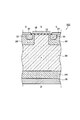
- a schematic cross-sectional structure of SiC • MOSFET is a semiconductor substrate 26 made of an n ⁇ high resistance layer.
- a p base region 28 formed on the surface side of the semiconductor substrate 26, a source region 30 formed on the surface of the p base region 28, and a gate disposed on the surface of the semiconductor substrate 26 between the p base regions 28.
- An n + drain region 24 and a drain pad electrode 36 connected to the n + drain region 24 are provided.
- the semiconductor device 100 is composed of a planar gate type n-channel vertical SiC • MOSFET, but may be composed of a trench gate type n-channel vertical SiC • MOSFET.
- SiC • MOSFET Si-based MOSFET, GaN-based FET, or the like can be applied to the semiconductor device 100 applied to the power module semiconductor device 1 according to the first embodiment.
- any one of Si, SiC, GaN, or AlN power devices can be applied.
- the semiconductor device 100 applied to the power module semiconductor device 1 according to the first embodiment can use a semiconductor having a band gap energy of, for example, 1.1 eV to 8 eV.
- FIG. 32 is an example of the semiconductor device 100 applied to the power module semiconductor device 1 according to the first embodiment, and a schematic cross-sectional structure of the SiC MOSFET including the source pad electrode SP and the gate pad electrode GP is shown in FIG. It is expressed as follows.
- the gate pad electrode GP is connected to the gate electrode 38 disposed on the gate insulating film 32, and the source pad electrode SP is connected to the source electrode 34 connected to the source region 30 and the p base region 28.
- the gate pad electrode GP and the source pad electrode SP are disposed on a passivation interlayer insulating film 44 covering the surface of the semiconductor device 100.
- illustration is omitted in the configuration example of FIG. 32, but as in the central portion of FIG. 31 or FIG. A transistor structure having a structure may be formed.
- the source pad electrode SP may be extended and disposed on the passivation interlayer insulating film 44.
- the gate pad electrode GP may be extended and disposed on the passivation interlayer insulating film 44.
- FIG. 33A A schematic external plan configuration of the power module semiconductor device 1 according to the modification 12 of the first embodiment is expressed as shown in FIG. 33A, and the back configuration of FIG. 33A is shown in FIG. It is expressed as shown in b).
- the back surface configuration of the power module semiconductor device 1 according to the modification 12 of the first embodiment is the same as the back surface configuration of the modification 1 of the first embodiment.
- the power module semiconductor device 1 according to the modified example 12 of the first embodiment has a configuration in which the sides of the ceramic substrate on which the output terminal electrodes UL, VL, and WL are arranged are changed as compared with the first embodiment.
- the power module semiconductor device 1 includes a ceramic substrate 10, a first plate layer 10a, and a second plate. 10b, low-voltage side gate terminal electrodes GL4, GL5, and GL6, low-voltage side source terminal electrodes SL4, SL5, and SL6, high-voltage side gate terminal electrodes GL1, GL2, and GL3, and high-voltage side source terminal electrodes SL1, SL2, and SL3 Output terminal electrodes UL, VL, WL, power supply voltage supply terminal electrode PL, and ground potential terminal electrode NL.
- the first plate layer 10 a is disposed on the surface of the ceramic substrate 10.
- the 2nd plate layer and 10b are arrange
- the low-voltage side gate terminal electrodes GL4, GL5, and GL6 are disposed on the first side of the ceramic substrate.
- the low-voltage side source terminal electrodes SL4, SL5, and SL6 are arranged on the first side and are arranged adjacent to the low-voltage side gate terminal electrodes GL4, GL5, and GL6, respectively.
- the high-voltage side gate terminal electrodes GL1, GL2, and GL3 are arranged on the first side, and are separated from the low-voltage side gate terminal electrodes GL4, GL5, and GL6 and the low-voltage side source terminal electrodes SL4, SL5, and SL6.
- the high-voltage side source terminal electrodes SL1, SL2, and SL3 are arranged on the first side and are arranged adjacent to the high-voltage side gate terminal electrodes GL1, GL2, and GL3, respectively.
- the output terminal electrodes UL, VL, WL are arranged on a second side different from the first side of the ceramic substrate.
- the power supply voltage supply terminal electrode PL is disposed on the third side of the ceramic substrate facing the second side.
- the ground potential terminal electrode NL is disposed on the third side and is separated from the power supply voltage supply terminal electrode PL.
- the twelfth modification of the first embodiment it is possible to provide a power module semiconductor device that realizes a reduction in warpage due to downsizing of a transfer mold and reduction of thermal stress.
- FIG. 34A A schematic external plan configuration of the power module semiconductor device 1 according to the modified example 13 of the first embodiment is represented as shown in FIG. 34A, and the back configuration of FIG. It is expressed as shown in b).
- the power module semiconductor device 1 according to the modification 13 of the first embodiment further includes a side where the power supply voltage supply terminal electrode PL and the ground potential terminal electrode NL are arranged as compared with the modification 12 of the first embodiment. The configuration is changed.
- the power module semiconductor device 1 includes a ceramic substrate 10, a first plate layer 10a, and a second plate.
- Layer 10b low-voltage side gate terminal electrodes GL4, GL5, GL6, low-voltage side source terminal electrodes SL4, SL5, SL6, high-voltage side gate terminal electrodes GL1, GL2, GL3, and high-voltage side source terminal electrodes SL1, SL2, SL3, output terminal electrodes UL, VL, WL, power supply voltage supply terminal electrode PL, and ground potential terminal electrode NL are provided.
- the first plate layer 10 a is disposed on the surface of the ceramic substrate 10.
- the 2nd plate layer and 10b are arrange
- the low-voltage side gate terminal electrodes GL4, GL5, and GL6 are disposed on the first side of the ceramic substrate.
- the low-voltage side source terminal electrodes SL4, SL5, and SL6 are arranged on the first side and are arranged adjacent to the low-voltage side gate terminal electrodes GL4, GL5, and GL6, respectively.
- the high-voltage side gate terminal electrodes GL1, GL2, and GL3 are arranged on the first side, and are separated from the low-voltage side gate terminal electrodes GL4, GL5, and GL6 and the low-voltage side source terminal electrodes SL4, SL5, and SL6.
- the high-voltage side source terminal electrodes SL1, SL2, and SL3 are arranged on the first side and are arranged adjacent to the high-voltage side gate terminal electrodes GL1, GL2, and GL3, respectively.
- the output terminal electrodes UL, VL, WL are arranged on a second side different from the first side of the ceramic substrate.
- the power supply voltage supply terminal electrode PL is disposed on the third side of the ceramic substrate facing the first side.
- the ground potential terminal electrode NL is disposed on the third side and is separated from the power supply voltage supply terminal electrode PL.
- the thirteenth modification of the first embodiment it is possible to provide a power module semiconductor device that realizes a reduction in warpage due to downsizing of the transfer mold and reduction of thermal stress.
- FIG. 35A A schematic external plan configuration of the power module semiconductor device 1 according to the modified example 14 of the first embodiment is represented as shown in FIG. 35A, and the back configuration of FIG. It is expressed as shown in b).
- the power module semiconductor device 1 according to the modification 14 of the first embodiment has a configuration corresponding to a single-phase inverter in terms of circuit configuration.
- the power module semiconductor device 1 includes a ceramic substrate 10, a first plate layer 10a, and a second plate.
- Layer 10b low voltage side gate terminal electrode GL4, low voltage side source terminal electrode SL4, high voltage side gate terminal electrode GL1, high voltage side source terminal electrode SL1, output terminal electrode UL, and power supply voltage supply terminal electrode PL And a ground potential terminal electrode NL.
- the first plate layer 10 a is disposed on the surface of the ceramic substrate 10.
- the 2nd plate layer and 10b are arrange
- the low-voltage side gate terminal electrode GL4 is disposed on the first side of the ceramic substrate.
- the low-voltage side source terminal electrode SL4 is disposed on the first side and adjacent to the low-voltage side gate terminal electrode GL4.
- the high-voltage side gate terminal electrode GL1 is arranged on the first side and is arranged apart from the low-voltage side gate terminal electrode GL4 and the low-voltage side source terminal electrode SL4.
- the high-voltage side source terminal electrode SL1 is disposed on the first side and is disposed adjacent to the high-voltage side gate terminal electrode GL1.
- the output terminal electrode UL is disposed on the second side opposite to the first side of the ceramic substrate.
- Power supply voltage supply terminal electrode PL is arranged on the third side of the ceramic substrate different from the first side and the second side.
- the ground potential terminal electrode NL is disposed on the third side and is separated from the power supply voltage supply terminal electrode PL.
- the modification 14 of the first embodiment it is possible to provide a power module semiconductor device that realizes a reduction in warpage due to a reduction in size of a transfer mold and a reduction in thermal stress.
- FIG. 36A a schematic external plan configuration of the power module semiconductor device 1 according to the modification 15 of the first embodiment is represented as shown in FIG. 36A, and the back configuration of FIG. It is expressed as shown in 36 (b).
- the power module semiconductor device 1 according to the modification 15 of the first embodiment has a configuration in which the sides of the ceramic substrate on which the output terminal electrodes UL are arranged are changed as compared with the modification 14 of the first embodiment.
- the power module semiconductor device 1 according to the modification 15 of the first embodiment also has a configuration corresponding to a single-phase inverter in terms of circuit configuration.
- the power module semiconductor device 1 includes a ceramic substrate 10, a first plate layer 10a, and a second plate.
- Layer 10b low voltage side gate terminal electrode GL4, low voltage side source terminal electrode SL4, high voltage side gate terminal electrode GL1, high voltage side source terminal electrode SL1, output terminal electrode UL, and power supply voltage supply terminal electrode PL And a ground potential terminal electrode NL.
- the first plate layer 10 a is disposed on the surface of the ceramic substrate 10.
- the 2nd plate layer and 10b are arrange
- the low-voltage side gate terminal electrode GL4 is disposed on the first side of the ceramic substrate.
- the low-voltage side source terminal electrode SL4 is disposed on the first side and adjacent to the low-voltage side gate terminal electrode GL4.
- the high-voltage side gate terminal electrode GL1 is arranged on the first side and is arranged apart from the low-voltage side gate terminal electrode GL4 and the low-voltage side source terminal electrode SL4.
- the high-voltage side source terminal electrode SL1 is disposed on the first side and is disposed adjacent to the high-voltage side gate terminal electrode GL1.
- the output terminal electrode UL is disposed on a second side different from the first side of the ceramic substrate.
- the power supply voltage supply terminal electrode PL is arranged on the third side of the ceramic substrate facing the second side.
- the ground potential terminal electrode NL is disposed on the third side and is separated from the power supply voltage supply terminal electrode PL.
- the fifteenth modification of the first embodiment it is possible to provide a power module semiconductor device that realizes a reduction in warpage due to downsizing of the transfer mold and reduction of thermal stress.
- FIG. 1 a schematic bird's-eye view showing a structure in which terminal electrodes, transistors, and diodes are mounted is expressed as shown in FIG. Further, a schematic planar pattern configuration showing a structure in which the terminal electrodes, transistors, and diodes of the power module semiconductor device 1 according to the second embodiment are mounted is expressed as shown in FIG. The circuit configuration of the power module semiconductor device 1 according to the embodiment is expressed in the same manner as in FIG.
- the ceramic substrate 10 is divided into a plurality of parts.
- the module when the module is manufactured by transfer molding, the module is prevented from being deformed due to the difference in expansion coefficient between the sealing resin and the ceramic substrate 10 therein.
- the ceramic substrate 10 inside is divided. That is, by dividing the ceramic substrate 10 into a plurality of pieces and making the ceramic substrates small and molding them, the transfer mold module is less likely to be deformed, and the transfer mold module is less likely to warp.
- corner portion of the ceramic substrate 10 may have a tapered shape or a curved shape. This is because the transfer mold resin 12 can be effectively injected between the divided ceramic substrates 10 in the injection process of the transfer mold resin 12.
- the ceramic substrate 10 is divided into five pieces: SEE, SEH, SEL, SEV, and SEW.
- a ground plate electrode EP connected to the ground potential terminal electrode NL is disposed on the ceramic substrate SEE.
- source terminal plate electrodes SLP1 to SLP6 and gate terminal plate electrodes GLP1 to GLP6 connected to the source terminal electrodes SL1 to SL6 and the gate terminal electrodes GL1 to GL6 are arranged.
- a drain electrode pattern D (K) connected to the power supply voltage supply terminal electrode PL is disposed on the ceramic substrate SEH.
- a drain electrode pattern D (K4) connected to the output terminal electrode UL is arranged on the ceramic substrate SEL, and a drain electrode pattern D (K5) connected to the output terminal electrode UV is arranged on the ceramic substrate SEV.
- the drain electrode pattern D (K6) connected to the output terminal electrode UW is disposed on the ceramic substrate SEW.
- the schematic external plane configuration of the power module semiconductor device 1 according to the second embodiment is represented in the same manner as in FIG. 1, and the back surface configuration is the second plate layer disposed on the back surface of the divided ceramic substrate 10. It is expressed similarly to the pattern configuration of 10b.
- the power module semiconductor device 1 includes a ceramic substrate 10 (SEE, SEH, SEL, SEV, SEW) divided into a plurality of parts, a first plate layer 10a, a second plate layer 10b, Low voltage side gate terminal electrodes GL4, GL5, GL6, Low voltage side source terminal electrodes SL4, SL5, SL6, High voltage side gate terminal electrodes GL1, GL2, GL3, High voltage side source terminal electrodes SL1, SL2, SL3, and output terminals Electrodes UL, VL, WL, a power supply voltage supply terminal electrode PL, and a ground potential terminal electrode NL are provided.
- a ceramic substrate 10 SEE, SEH, SEL, SEV, SEW
- the first plate layer 10a is disposed on the surface of a plurality of divided ceramic substrates 10 (SEE, SEH, SEL, SEV, SEW), and the second plate layer 10b is divided into a plurality of divided ceramic substrates 10 (SEE, SEH, SEL, SEV, SEW) are arranged on the back surface.
- the first plate layer 10a and the second plate layer 10b can be formed of, for example, a copper plate layer.
- a DBC substrate can be applied to the substrate structure composed of the ceramic substrate 10, the first plate layer 10a, and the second plate layer 10b. Or it can form by affixing the 1st plate layer 10a and the 2nd plate layer 10b suitably to the surface and back surface of the ceramic substrate 10 divided
- the low-voltage side gate terminal electrodes GL4, GL5, and GL6 are disposed on the first side of the ceramic substrate SEE.
- the low-voltage side source terminal electrodes SL4, SL5, and SL6 are arranged on the first side of the ceramic substrate SEE and are arranged adjacent to the low-voltage side gate terminal electrodes GL4, GL5, and GL6, respectively.
- the high-voltage side gate terminal electrodes GL1, GL2, and GL3 are arranged on the first side of the ceramic substrate SEE, and are separated from the low-voltage side gate terminal electrodes GL4, GL5, and GL6 and the low-voltage side source terminal electrodes SL4, SL5, and SL6. Be placed.
- the high-voltage side source terminal electrodes SL1, SL2, and SL3 are arranged on the first side of the ceramic substrate SEE and are arranged adjacent to the high-voltage side gate terminal electrodes GL1, GL2, and GL3, respectively.
- the output terminal electrodes UL, VL, WL are arranged on the second side opposite to the first side of the ceramic substrate SEL, SEV, SEW.
- the power supply voltage supply terminal electrode PL is arranged on the third side of the ceramic substrate SEH different from the first side of the ceramic substrate SEE and the second side of the ceramic substrate SEL / SEV / SEW.
- the ground potential terminal electrode NL is disposed on the third side of the ceramic substrate SEE different from the first side of the ceramic substrate SEE and is separated from the power supply voltage supply terminal electrode PL.
- the ceramic substrate 10 can be formed of any one of aluminum oxide (Al 2 O 3 ), aluminum nitride (AlN), and silicon nitride (SiN).
- the ceramic substrate 10 / first plate layer 10a and second plate layer 10b can be formed of any one of an aluminum oxide substrate / Cu plate electrode, an aluminum nitride substrate / Al plate electrode, and a silicon nitride substrate / Cu plate electrode. .
- Examples of the combination of the ceramic substrate 10 / second plate layer 10b functioning as a heat sink include an alumina substrate / Cu plate electrode, an aluminum nitride substrate / Al plate electrode, a silicon nitride substrate / Cu plate electrode, and the like. .
- the aluminum nitride substrate is characterized by low thermal resistance.
- the thermal resistance of the silicon nitride substrate is about 1/3 that of the aluminum nitride substrate, and the high temperature characteristics are also good.
- the combination of the alumina substrate / Cu plate electrode is the cheapest.
- the power module semiconductor device 1 when a module is manufactured by transfer molding, a plurality of ceramic substrates 10 are used in order to suppress deformation of the module due to thermal stress in a high temperature environment. By dividing and covering the grooves between the divided ceramic substrates 10 with resin, the stress and the deformation amount of the module can be reduced.
- the ceramic substrate 10 is divided into a plurality of parts, and the resin is applied to the grooves between the divided ceramic substrates 10 and both the front and back surfaces of the transfer mold module. By turning around, deformation can be reduced and stress can be reduced.
- a transfer mold module is formed in order to reduce the size.
- the terminal electrode can be taken out from the three directions of the mold package to obtain an insulation distance.
- the signal terminal on the high voltage side is arranged away from the signal terminal on the low voltage side during the inverter operation, and the signal terminal on the low voltage side is arranged in part.
- the low voltage side signal terminals are arranged side by side, the high voltage side signal terminals are arranged apart from each other, the output terminals are arranged apart from the low voltage side and high voltage side signal terminals, and the power supply voltage
- the terminal and the ground potential terminal are arranged separately from the output terminal and the signal terminal.
- the power supply voltage terminal, the ground potential terminal, the low-voltage side and the high-voltage side signal terminal and the output terminal are taken out from the three directions of the transfer mold module package to increase the insulation distance It can also be taken.
- the power supply voltage supply terminal electrode PL and the ground potential terminal electrode NL are arranged adjacent to each other in order to facilitate the connection between the power supply V and the capacitor C. .
- the width of the output terminal electrodes UL, VL, and WL may be set wide in a portion where strain stress is applied when the resin of the transfer mold resin is injected. That is, in the power module semiconductor device 1 according to the second embodiment, a resin injection gate is formed on the power terminal side of the high heat resistant mold module, and a protrusion for preventing slippage is provided on the power terminal of the high heat resistant mold module. It may be produced.
- the power bonding wire on the power terminal side is thicker than the signal wire bonding wire, it is desirable to inject the resin of the high heat resistant resin from the power terminal side. Moreover, in order to raise the intensity
- the first plate layer 10a includes the low-voltage side gate terminal electrode patterns GLP4, GLP5, and GLP6, as shown in FIGS.
- Low voltage side on which source terminal electrode patterns SLP4, SLP5, SLP6, high voltage side gate terminal electrode patterns GLP1, GLP2, GLP3, high voltage side source terminal electrode patterns SLP1, SLP2, SLP3, and low voltage side transistors Q4, Q5, Q6 are mounted
- Drain electrode patterns D (K4), D (K5), and D (K6), high-voltage side drain electrode patterns D (K) on which high-voltage side transistors Q1, Q2, and Q3 are mounted, and a ground electrode pattern EP are provided.
- the low-voltage drain electrode patterns D (K4), D (K5), and D (K6) are arranged as shown in FIGS. Is mounted with low-voltage side diodes D4, D5, and D6 connected in reverse parallel to the low-voltage side transistors Q4, Q5, and Q6, and the high-voltage side drain electrode pattern D (K) is reverse to the high-voltage side transistors Q1, Q2, and Q3. High-voltage side diodes D1, D2, and D3 connected in parallel are mounted.
- the chip size of the transistors Q1, Q2, Q3, Q4, Q5, and Q6 is, for example, about 5 mm ⁇ 5 mm, and the thickness is, for example, about 0.25 mm.
- the chip size of the diodes D1, D2, D3, D4, D5, and D6 is, for example, about 5 mm ⁇ 5 mm, and the thickness is, for example, about 0.25 mm.
- the chip size is not limited to this, and may be, for example, 4 mm square to 6 mm square.
- the thickness of the ground electrode pattern EP is, for example, about 0.3 to 0.4 mm.
- the thickness of each terminal electrode is about 0.2 mm, for example.
- the thickness of the solder layers 14 and 15 is, for example, about 0.1 mm.
- the power module semiconductor device 1 includes a first bonding wire SW4, SW5, SW6, a second bonding wire GW4, GW5, GW6, and a third bonding wire.
- first bonding wires SW4, SW5, and SW6 connect the low-voltage side source terminal electrode patterns SLP4, SLP5, and SLP6 to the source pad electrodes SP4, SP5, and SP6 of the low-voltage side transistors Q4, Q5, and Q6.
- the second bonding wires GW4, GW5, and GW6 connect the low-voltage side gate terminal electrode patterns GLP4, GLP5, and GLP6 to the gate pad electrodes GP4, GP5, and GP6 of the low-voltage side transistors Q4, Q5, and Q6.
- the third bonding wires SW1, SW2, and SW3 connect the high-voltage side source terminal electrode patterns SLP1, SLP2, and SLP3 to the source pad electrodes SP1, SP2, and SP3 of the high-voltage side transistors Q1, Q2, and Q3.
- the fourth bonding wires GW1, GW2, and GW3 connect the high-voltage side gate terminal electrode patterns GLP1, GLP2, and GLP3 to the gate pad electrodes GP1, GP2, and GP3 of the high-voltage side transistors Q1, Q2, and Q3.
- the fifth bonding wires AW4, AW5, and AW6 include the ground electrode pattern EP, the source pad electrodes SP4, SP5, and SP6 of the low-voltage side transistors Q4, Q5, and Q6, and the anode electrodes A4, A5, and A6 of the low-voltage side diodes D4, D5, and D6. And the stitch bonding connection.
- the sixth bonding wires AW1, AW2, and AW3 connect the source pad electrodes SP1, SP2, and SP3 of the high-voltage side transistors Q1, Q2, and Q3 to the anode electrodes A1, A2, and A3 of the high-voltage side diodes D1, D2, and D3.
- the seventh bonding wires BW1, BW2, and BW3 connect the anode electrodes A1, A2, and A3 of the high-voltage side diodes D1, D2, and D3 to the low-voltage side drain electrode patterns D (K4), D (K5), and D (K6).
- the sixth bonding wires AW1, AW2, and AW3 and the seventh bonding wires BW1, BW2, and BW3 may be stitch-bonded.
- the low-voltage side gate terminal electrode patterns GLP4, GLP5, and GLP6 are mounted with the low-voltage side gate terminal electrodes GL4, GL5, and GL6, and the low-voltage side source terminal electrode patterns SLP4, SLP5, and Low-voltage side source terminal electrodes SL4, SL5, and SL6 are mounted on SLP6, and high-voltage side gate terminal electrodes GL1, GL2, and GL3 are mounted on high-voltage side gate terminal electrode patterns GLP1, GLP2, and GLP3.
- the electrode patterns SLP1, SLP2, and SLP3 have high-voltage side source terminal electrodes SL1, SL2, and SL3 mounted thereon, the ground electrode pattern EP has a ground potential terminal electrode NL mounted thereon, and the high-voltage side drain electrode pattern D (K). Is provided with a power supply voltage supply terminal electrode PL and a low-voltage drain electrode pattern D (K ) The ⁇ D (K5) ⁇ D (K6), the output terminal electrode UL ⁇ VL ⁇ WL is mounted.
- the output terminal electrodes UL, VL, and WL include output terminal electrode expansion portions UE, VE, and WE for increasing the strength. May be.
- the power supply voltage supply terminal electrode PL and the ground potential terminal electrode NL have power supply voltage supply terminal electrodes for increasing the strength, as shown in FIG.
- the extended portion PLE and the ground potential terminal electrode extended portion NLE may be provided.
- the electrode expansion portions for increasing the strength include the high-voltage side gate terminal electrodes GL1, GL2, and GL3, the high-voltage side source terminal electrodes SL1, SL2, and SL3, and the low-voltage side gate terminal electrode GL4. -You may form in each connection part of GL5 * GL6 and low voltage
- the second plate layer 10b is formed on the front and back surfaces of the ceramic substrate 10 as shown in FIGS.
- a transfer mold resin 12 is provided except for the above.
- FIG. 39 to 44, 46 (a), and 46 (b) A schematic planar pattern configuration of the power module semiconductor device 1 according to the second embodiment corresponding to the step of FIG. 44 is expressed as shown in FIG.
- the substrate structure of the power module semiconductor device 1 according to the second embodiment is the same as the ceramic substrate 10, the first plate layer 10a, and the second plate as shown in FIG.
- a DBC substrate made of the layer 10b can be applied.
- the first plate layer 10a and the second plate layer 10b can be formed of, for example, a copper plate layer.
- the method of manufacturing the power module semiconductor device 1 according to the second embodiment includes a step of dividing the ceramic substrate 10 into a plurality of parts, and a surface of the divided ceramic substrates SEE / SEH / SEW. There are a step of forming the first plate layer 10a thereon and a step of forming the second plate layer 10b on the back surface of the divided ceramic substrates SEE / SEH / SEW.
- the first plate layer 10a on the surface of the plurality of ceramic substrates SEE / SEH / SEW is patterned, On the first side of the ceramic substrate SEE, the low side gate terminal electrode patterns GLP4, GLP5, GLP6, the low side source terminal electrode patterns SLP4, SLP5, SLP6, the high side gate terminal electrode patterns GLP1, GLP2, GLP3, and the high side
- the source terminal electrode patterns SLP1, SLP2, and SLP3 are formed and separated from the first side of the ceramic substrate SEE, and the low-voltage drain electrode patterns D (K4) and D (K5) are formed on the ceramic substrates SEL, SEV, and SEW.
- D Forming a pattern D (K), a step of forming a ground electrode pattern EP on the ceramic substrate SEE on.
- the method for manufacturing the power module semiconductor device 1 according to the second embodiment includes a low voltage side on the low voltage side drain electrode patterns D (K4), D (K5), and D (K6).
- the low-voltage side diodes D4, D5, and D6 connected in reverse parallel to the transistors Q4, Q5, and Q6 and the low-voltage side transistors Q4, Q5, and Q6 are mounted.
- the low voltage side gate terminal electrode patterns GLP4, GLP5, and GLP6 are connected to the low voltage side on the first side of the ceramic substrate SEE.
- the gate terminal electrodes GL4, GL5, GL6 are connected, the low voltage side source terminal electrode patterns SLP4, SLP5, SLP6 are connected to the low voltage side source terminal electrodes SL4, SL5, SL6, and the high voltage side gate terminal electrode patterns GLP1, GLP2, GLP3 are connected.
- the high-voltage side gate terminal electrodes GL1, GL2, and GL3 are connected, and the high-voltage side source terminal electrode patterns SLP1, SLP2, and SLP3 are connected to the high-voltage side source terminal electrodes SL1, SL2, and SL3, and separated from the first side of the ceramic substrate SEE Side of the ceramic substrate SEL / SEV / SEW
- the output terminal electrodes UL, VL, and WL are connected to the rain electrode patterns D (K4), D (K5), and D (K6), and the first side of the ceramic substrate SEE and the second side of the ceramic substrate SEL, SEV, and SEW are connected.
- the ground potential terminal electrode NL is connected to the ground electrode pattern EP on the third side of the ceramic substrate SEE different from the side, and the ceramic is different from the first side of the ceramic substrate SEE and the second side of the ceramic substrate SEL / SEV / SEW.
- the method for manufacturing the power module semiconductor device 1 according to the second embodiment includes the source pads of the low-voltage side source terminal electrode patterns SLP4, SLP5, and SLP6 and the low-voltage side transistors Q4, Q5, and Q6.
- the electrodes SP4, SP5, and SP6 are connected using bonding wires SW4, SW5, and SW6, and the gate pad electrodes GP4, GP5, and GP6 of the low-voltage side gate terminal electrode patterns GLP4, GLP5, and GLP6 and the low-voltage side transistors Q4, Q5, and Q6 are connected.
- the high-voltage side gate terminal electrode patterns GLP1, GLP2, and GLP3 are connected to the gate pad electrodes GP1, GP2, and GP3 of the high-voltage side transistors Q1, Q2, and Q3 using bonding wires GW1, GW2, and GW3, and the ground electrode pattern EP and the low voltage are connected.
- the source pad electrodes SP4, SP5, and SP6 of the side transistors Q4, Q5, and Q6 and the anode electrodes A4, A5, and A6 of the low-voltage side diodes D4, D5, and D6 are stitch-bonded using bonding wires AW4, AW5, and AW6,
- the source pad electrodes SP1, SP2, and SP3 of the high-voltage side transistors Q1, Q2, and Q3 and the anode electrodes A1, A2, and A3 of the high-voltage side diodes D1, D2, and D3 are connected using bonding wires AW1, AW2, and AW3.
- bonding wires SW1, SW2, SW3, SW4, SW5, SW6 and bonding wires GW1, GW2, GW3, GW4, GW5, and GW6 use relatively thin bonding wires.
- Bonding wires AW1, AW2, AW3, AW4, AW5, and AW6 and bonding wires BW1, BW2, and BW3 use relatively thick bonding wires. Although shown as one in the drawing, for example, about four relatively thick bonding wires may be connected in parallel.
- the relatively thick bonding wire connection before the relatively thin bonding wire connection. Further, it is desirable to perform the bonding wire connection between the transistors Q1, Q2, Q3, Q4, Q5, and Q6 and the diodes D1, D2, D3, D4, D5, and D6 before the bonding wire connection of the terminal electrode pattern. . This is to prevent the relatively thin bonding wire from being damaged by the force applied when the relatively thick bonding wire is connected.
- the low-voltage drain electrode patterns D (K4) and D (K5) of the ceramic substrate 10 are used. ).
- FIGS. 39 to 44, FIG. 46A and FIG. 46B show schematic cross-sectional structures taken along line IV-IV in FIG.
- the ceramic substrate 10 is divided into a plurality of parts to form ceramic substrates SEE / SEH / SEW, and the first plate layer 10a is formed on the surface of the ceramic substrate SEE / SEH / SEW. Then, the second plate layer 10b is formed on the back surface of the ceramic substrate SEE / SEH / SEW.
- the first plate layer 10a is patterned to form a high-voltage side source terminal electrode pattern SLP3, a ground electrode pattern EP, a high-voltage side drain electrode pattern D (K), and a low-voltage side drain electrode.
- a pattern D (K6) is formed.
- the high voltage side transistor Q3 and the high voltage side diode D3 are mounted on the high voltage side drain electrode pattern D (K) via the solder layer 15.
- the high voltage side transistor Q3 and the high voltage side diode D3 are connected in reverse parallel to each other, and the high voltage side drain electrode pattern D (K) is connected to the drain electrode of the high voltage side transistor Q3 and the cathode electrode of the high voltage side diode D3.
- the high-voltage side source terminal electrode SL3 is connected to the high-voltage side source terminal electrode pattern SLP3 via the solder layer 14, and the low-voltage side drain electrode pattern D (K6) is formed.
- the output terminal electrode WL is connected through the solder layer 16.
- the high-voltage source terminal electrode pattern SLP3 and the source pad electrode SP3 of the high-voltage transistor Q3 are connected using a bonding wire SW3, and the source pad electrode SP3 of the high-voltage transistor Q3 is connected.
- the anode electrode A3 of the high-voltage side diode D3 are connected using a bonding wire AW3, and the anode electrode A3 of the high-voltage side diode D3 and the low-voltage side drain electrode pattern D (K6) are connected using a bonding wire BW3.
- the low-voltage source terminal electrode patterns SLP4, SLP5, and SLP6 and the source pad electrodes SP4, SP5, and SP6 of the low-voltage transistors Q4, Q5, and Q6 are bonded to the bonding wires SW4 and SW5. -Connect using SW6.
- the low-voltage side gate terminal electrode patterns GLP4, GLP5, and GLP6 are connected to the gate pad electrodes GP4, GP5, and GP6 of the low-voltage side transistors Q4, Q5, and Q6 using bonding wires GW4, GW5, and GW6.
- the high-voltage side source terminal electrode patterns SLP1, SLP2, and SLP3 are connected to the source pad electrodes SP1, SP2, and SP3 of the high-voltage side transistors Q1, Q2, and Q3 using bonding wires SW1, SW2, and SW3.
- the high-voltage side gate terminal electrode patterns GLP1, GLP2, and GLP3 and the gate pad electrodes GP1, GP2, and GP3 of the high-voltage side transistors Q1, Q2, and Q3 are connected using bonding wires GW1, GW2, and GW3.
- ground electrode pattern EP and the source pad electrodes SP4, SP5, and SP6 of the low-voltage side transistors Q4, Q5, and Q6 and the anode electrodes A4, A5, and A6 of the low-voltage side diodes D4, D5, and D6 are bonded to the bonding wires AW4, AW5, and AW6. Connect with stitch bonding.
- the source pad electrodes SP1, SP2, and SP3 of the high-voltage side transistors Q1, Q2, and Q3 and the anode electrodes A1, A2, and A3 of the high-voltage side diodes D1, D2, and D3 are bonded using bonding wires AW1, AW2, and AW3.
- the anode electrodes A1, A2, and A3 of the high-voltage side diodes D1, D2, and D3 and the low-voltage side drain electrode patterns D (K4), D (K5), and D (K6) are stitch-bonded using bonding wires BW1, BW2, and BW3. Connecting.
- bonding wire AW1 and the bonding wire BW1 may be stitch-bonded continuously with one bonding wire.
- bonding wire AW2 and bonding wire BW2 may be stitch-bonded continuously with one bonding wire.
- bonding wire AW3 and bonding wire BW3 may be stitch-bonded continuously with one bonding wire.
- the portion indicated by the bonding wire AW4 is different between the ground electrode pattern EP and the source pad electrode SP4 of the low voltage side transistor Q4, and between the source pad electrode SP4 of the low voltage side transistor Q4 and the anode electrode A4 of the low voltage side diode D4.
- Wire bonding connection may be performed using a bonding wire. The same applies to the bonding wire AW5 and the bonding wire AW6.
- transfer mold resin 12 is injected from the side of the ceramic substrate 10 (SEW) where the low-voltage drain electrode pattern D (K6) is disposed.
- the low-voltage drain electrode patterns D (K4), D (K5), and D (K6) of the ceramic substrate 10 are formed.
- Transfer mold resin 12 is injected from the opposite side.
- a thermosetting epoxy resin can be applied as a material of the transfer mold resin 12.
- the gate bonding wires (thin wire wires) GW4, GW5, and GW6 that connect the low-voltage side gate terminal electrode patterns GLP4, GLP5, and GLP6 to the gate pad electrodes GP4, GP5, and GP6 of the low-voltage side transistors Q4, Q5, and Q6 are opposed to each other.
- Transfer mold resin 12 may be injected from the direction.
- the transfer mold resin 12 is formed on the front and back surfaces of the plurality of ceramic substrates 10.
- the transfer mold resin 12 is formed so as to cover the front and back surfaces of the plurality of ceramic substrates 10 except on the second plate layer 10b. That is, the transfer mold resin 12 is also formed in the groove portions between the divided second plate layers 10 b and between the plurality of ceramic substrates 10 on the back surfaces of the plurality of ceramic substrates 10.
- the power module semiconductor device 1 according to the second embodiment is completed.
- the peripheral portion of the transfer mold resin 12 has an angle ⁇ .
- the value of the angle ⁇ is, for example, about 70 to 85 degrees.
- the second embodiment it is possible to provide a power module semiconductor device that realizes a reduction in warpage by reducing the size of a transfer mold and reducing thermal stress.
- FIG. 1 a schematic bird's-eye view configuration showing a structure in which terminal electrodes, transistors, and diodes are mounted is expressed as shown in FIG. Further, a schematic plane pattern configuration showing a structure in which the terminal electrodes, transistors, and diodes of the power module semiconductor device 1 according to the third embodiment are mounted is expressed as shown in FIG. The circuit configuration of the power module semiconductor device 1 according to the embodiment is expressed in the same manner as in FIG.
- the ceramic substrate 10 is divided into a plurality of parts.
- the module when the module is manufactured by transfer molding, the module is prevented from being deformed due to the difference in expansion coefficient between the sealing resin and the ceramic substrate 10 therein.
- the ceramic substrate 10 inside is divided. That is, the ceramic substrate 10 is divided into a plurality of pieces, and each ceramic is made smaller and molded, so that the transfer mold module is hardly deformed, and the transfer mold module is hardly warped.
- corner portion of the ceramic substrate 10 may have a tapered shape or a curved shape. This is because the transfer mold resin 12 can be effectively injected between the divided ceramic substrates 10 in the injection process of the transfer mold resin 12.
- the ceramic substrate 10 is divided into four parts SE1, SE2, SE3, and SE4 as shown in FIGS.
- source terminal plate electrodes SLP1 to SLP6 and gate terminal plate electrodes GLP1 to GLP6 connected to the source terminal electrodes SL1 to SL6 and the gate terminal electrodes GL1 to GL6 are arranged on the ceramic substrate SE1.
- ground plate electrode EP connected to the ground potential terminal electrode NL is disposed on the adjacent ceramic substrates SE1 and SE2 across the ceramic substrate SE1 and SE2.
- drain electrode pattern D (K) connected to the power supply voltage supply terminal electrode PL is disposed over the adjacent ceramic substrates SE2 and SE3.
- a drain electrode pattern D (K4) connected to the output terminal electrode UL, a drain electrode pattern D (K5) connected to the output terminal electrode UV, and an output A drain electrode pattern D (K6) connected to the terminal electrode UW is disposed across the terminal electrode UW.
- the schematic external plane configuration of the power module semiconductor device 1 according to the third embodiment is expressed in the same manner as in FIG. 1, and the back surface configuration is the back surface of the divided ceramic substrate 10 (SE1, SE2, SE3, SE4). It is expressed in the same manner as the pattern configuration of the second plate layer 10b disposed on the top.
- the power module semiconductor device 1 includes a ceramic substrate 10 divided into a plurality of parts, a first plate layer 10a, a second plate layer 10b, and low-voltage side gate terminal electrodes GL4, GL5, and GL6. , Low-voltage side source terminal electrodes SL4, SL5, and SL6, high-voltage side gate terminal electrodes GL1, GL2, and GL3, high-voltage side source terminal electrodes SL1, SL2, and SL3, output terminal electrodes UL, VL, and WL, and power supply voltage supply A terminal electrode PL and a ground potential terminal electrode NL are provided.
- the first plate layer 10a is arranged on the surface of the ceramic substrate 10 divided into a plurality of parts, and the second plate layer 10b is arranged on the back surface of the ceramic substrate 10 divided into a plurality of parts (SE1, SE2, SE3, SE4).
- the first plate layer 10a and the second plate layer 10b can be formed of, for example, a copper plate layer.
- a DBC substrate can be applied to the substrate structure composed of the ceramic substrate 10, the first plate layer 10a, and the second plate layer 10b. Or it can form by affixing the 1st plate layer 10a and the 2nd plate layer 10b suitably to the surface and back surface of the ceramic substrate 10 divided
- the low-voltage side gate terminal electrodes GL4, GL5, and GL6 are disposed on the first side of the ceramic substrate SE1.
- the low-voltage side source terminal electrodes SL4, SL5, and SL6 are arranged on the first side of the ceramic substrate SE1, and are arranged adjacent to the low-voltage side gate terminal electrodes GL4, GL5, and GL6, respectively.
- the high-voltage side gate terminal electrodes GL1, GL2, and GL3 are disposed on the first side of the ceramic substrate SE1, and are separated from the low-voltage side gate terminal electrodes GL4, GL5, and GL6 and the low-voltage side source terminal electrodes SL4, SL5, and SL6. Be placed.
- the high-voltage side source terminal electrodes SL1, SL2, and SL3 are arranged on the first side of the ceramic substrate SE1, and are arranged adjacent to the high-voltage side gate terminal electrodes GL1, GL2, and GL3, respectively.
- the output terminal electrodes UL, VL, and WL are disposed on the second side of the ceramic substrate SE4 that faces the first side of the ceramic substrate SE1.
- the power supply voltage supply terminal electrode PL is arranged on the third side of the ceramic substrate SE3 different from the first side of the ceramic substrate SE1 and the second side of the ceramic substrate SE4.
- the ground potential terminal electrode NL is arranged on the third side of the ceramic substrates SE1 and SE2 different from the first side of the ceramic substrate SE1, and is arranged apart from the power supply voltage supply terminal electrode PL.
- the ceramic substrate 10 can be formed of any one of aluminum oxide (Al 2 O 3 ), aluminum nitride (AlN), and silicon nitride (SiN).
- the ceramic substrate 10 / first plate layer 10a and second plate layer 10b can be formed of any one of an aluminum oxide substrate / Cu plate electrode, an aluminum nitride substrate / Al plate electrode, and a silicon nitride substrate / Cu plate electrode. .
- Examples of the combination of the ceramic substrate 10 / second plate layer 10b functioning as a heat sink include an alumina substrate / Cu plate electrode, an aluminum nitride substrate / Al plate electrode, a silicon nitride substrate / Cu plate electrode, and the like. .
- the aluminum nitride substrate is characterized by low thermal resistance.
- the thermal resistance of the silicon nitride substrate is about 1/3 that of the aluminum nitride substrate, and the high temperature characteristics are also good.
- the combination of the alumina substrate / Cu plate electrode is the cheapest.
- the power module semiconductor device 1 when a module is manufactured by transfer molding, a plurality of ceramic substrates 10 are used in order to suppress deformation of the module due to thermal stress in a high temperature environment. By dividing and covering the grooves between the divided ceramic substrates 10 with resin, the stress and the deformation amount of the module can be reduced.
- the ceramic substrate 10 is divided into a plurality of parts, and the resin is formed on both the front and back surfaces of the groove and the transfer mold module between the divided ceramic substrates 10. By turning around, deformation can be reduced and stress can be reduced.
- a transfer mold module is formed in order to reduce the size.
- the terminal electrode can be taken out from the three directions of the mold package to obtain an insulation distance.
- the high-voltage side signal terminal is arranged away from the low-voltage side signal terminal, and the low-voltage side signal terminal is arranged in part.
- the low voltage side signal terminals are arranged side by side, the high voltage side signal terminals are arranged apart from each other, the output terminals are arranged apart from the low voltage side and high voltage side signal terminals, and the power supply voltage
- the terminal and the ground potential terminal are arranged separately from the output terminal and the signal terminal.
- the power supply voltage terminal, the ground potential terminal, the low-voltage side and the high-voltage side signal terminal and the output terminal are taken out from the three directions of the module package of the transfer mold to increase the insulation distance. It can also be taken.
- the power supply voltage supply terminal electrode PL and the ground potential terminal electrode NL are arranged adjacent to each other in order to facilitate the connection between the power supply V and the capacitor C. .
- the widths of the output terminal electrodes UL, VL, and WL may be set wide in a portion where strain stress is applied during resin injection of the transfer mold resin. That is, in the power module semiconductor device 1 according to the third embodiment, a resin injection gate is formed on the power terminal side of the high heat resistant mold module, and a protrusion for preventing slippage is provided on the power terminal of the high heat resistant mold module. It may be produced.
- the power bonding wire on the power terminal side is thicker than the signal wire bonding wire, it is desirable to inject the resin of the high heat resistant resin from the power terminal side. Moreover, in order to raise the intensity
- the first plate layer 10a includes the low-voltage side gate terminal electrode patterns GLP4, GLP5, and GLP6 and the low-voltage side, as shown in FIGS.
- Low voltage side on which source terminal electrode patterns SLP4, SLP5, SLP6, high voltage side gate terminal electrode patterns GLP1, GLP2, GLP3, high voltage side source terminal electrode patterns SLP1, SLP2, SLP3, and low voltage side transistors Q4, Q5, Q6 are mounted
- Drain electrode patterns D (K4), D (K5), and D (K6), high-voltage side drain electrode patterns D (K) on which high-voltage side transistors Q1, Q2, and Q3 are mounted, and a ground electrode pattern EP are provided.
- the low-voltage drain electrode patterns D (K4), D (K5), and D (K6) Is mounted with low-voltage side diodes D4, D5, and D6 connected in reverse parallel to the low-voltage side transistors Q4, Q5, and Q6, and the high-voltage side drain electrode pattern D (K) is reverse to the high-voltage side transistors Q1, Q2, and Q3. High-voltage side diodes D1, D2, and D3 connected in parallel are mounted.
- the chip size of the transistors Q1, Q2, Q3, Q4, Q5, and Q6 is, for example, about 5 mm ⁇ 5 mm, and the thickness is, for example, about 0.25 mm.
- the chip size of the diodes D1, D2, D3, D4, D5, and D6 is, for example, about 5 mm ⁇ 5 mm, and the thickness is, for example, about 0.25 mm.
- the chip size is not limited to this, and may be, for example, 4 mm square to 6 mm square.
- the thickness of the ground electrode pattern EP is, for example, about 0.3 to 0.4 mm.
- the thickness of each terminal electrode is about 0.2 mm, for example.
- the thickness of the solder layers 14 and 15 is, for example, about 0.1 mm.
- the power module semiconductor device 1 includes first bonding wires SW4, SW5, and SW6, second bonding wires GW4, GW5, and GW6, and a third bonding wire.
- first bonding wires SW4, SW5, and SW6 connect the low-voltage side source terminal electrode patterns SLP4, SLP5, and SLP6 to the source pad electrodes SP4, SP5, and SP6 of the low-voltage side transistors Q4, Q5, and Q6.
- the second bonding wires GW4, GW5, and GW6 connect the low-voltage side gate terminal electrode patterns GLP4, GLP5, and GLP6 to the gate pad electrodes GP4, GP5, and GP6 of the low-voltage side transistors Q4, Q5, and Q6.
- the third bonding wires SW1, SW2, and SW3 connect the high-voltage side source terminal electrode patterns SLP1, SLP2, and SLP3 to the source pad electrodes SP1, SP2, and SP3 of the high-voltage side transistors Q1, Q2, and Q3.
- the fourth bonding wires GW1, GW2, and GW3 connect the high-voltage side gate terminal electrode patterns GLP1, GLP2, and GLP3 to the gate pad electrodes GP1, GP2, and GP3 of the high-voltage side transistors Q1, Q2, and Q3.
- the fifth bonding wires AW4, AW5, and AW6 include the ground electrode pattern EP, the source pad electrodes SP4, SP5, and SP6 of the low-voltage side transistors Q4, Q5, and Q6, and the anode electrodes A4, A5, and A6 of the low-voltage side diodes D4, D5, and D6. And the stitch bonding connection.
- the sixth bonding wires AW1, AW2, and AW3 connect the source pad electrodes SP1, SP2, and SP3 of the high-voltage side transistors Q1, Q2, and Q3 to the anode electrodes A1, A2, and A3 of the high-voltage side diodes D1, D2, and D3.
- the seventh bonding wires BW1, BW2, and BW3 connect the anode electrodes A1, A2, and A3 of the high-voltage side diodes D1, D2, and D3 to the low-voltage side drain electrode patterns D (K4), D (K5), and D (K6).
- the sixth bonding wires AW1, AW2, and AW3 and the seventh bonding wires BW1, BW2, and BW3 may be stitch-bonded.
- the low-voltage side gate terminal electrode patterns GLP4, GLP5, and GLP6 are mounted with the low-voltage side gate terminal electrodes GL4, GL5, and GL6, and the low-voltage side source terminal electrode patterns SLP4, SLP5, and Low-voltage side source terminal electrodes SL4, SL5, and SL6 are mounted on SLP6, and high-voltage side gate terminal electrodes GL1, GL2, and GL3 are mounted on high-voltage side gate terminal electrode patterns GLP1, GLP2, and GLP3.
- the electrode patterns SLP1, SLP2, and SLP3 have high-voltage side source terminal electrodes SL1, SL2, and SL3 mounted thereon, the ground electrode pattern EP has a ground potential terminal electrode NL mounted thereon, and the high-voltage side drain electrode pattern D (K). Is provided with a power supply voltage supply terminal electrode PL and a low-voltage drain electrode pattern D (K ) The ⁇ D (K5) ⁇ D (K6), the output terminal electrode UL ⁇ VL ⁇ WL is mounted.
- the output terminal electrodes UL, VL, and WL include output terminal electrode extensions UE, VE, and WE for increasing the strength. May be.
- the power supply voltage supply terminal electrode PL and the ground potential terminal electrode NL have power supply voltage supply terminal electrodes for increasing the strength, as shown in FIG.
- the extended portion PLE and the ground potential terminal electrode extended portion NLE may be provided.
- the electrode expansion portions for increasing the strength include the high-voltage side gate terminal electrodes GL1, GL2, and GL3, the high-voltage side source terminal electrodes SL1, SL2, and SL3, and the low-voltage side gate terminal electrode GL4. -You may form in each connection part of GL5 * GL6 and low voltage
- the second plate layer 10b is formed on the front surface and the back surface of the ceramic substrate 10.
- a transfer mold resin 12 is provided except for the above.
- FIG. 49 to 54 A schematic planar pattern configuration of the power module semiconductor device 1 according to the third embodiment corresponding to the step of FIG. 54 is expressed as shown in FIG.
- the substrate structure of the power module semiconductor device 1 according to the third embodiment is the same as the ceramic substrate 10, the first plate layer 10a, and the second plate as shown in FIG.
- a DBC substrate made of the layer 10b can be applied.
- the first plate layer 10a and the second plate layer 10b can be formed of, for example, a copper plate layer.
- the manufacturing method of the power module semiconductor device 1 includes a step of dividing the ceramic substrate 10 into a plurality of steps, and a divided ceramic substrate 10 (SE1, SE2, SE3).
- the first plate layer 10a on the surface of the plurality of ceramic substrates 10 SE1, SE2, SE3, SE4.
- GLP3 and high-voltage side source terminal electrode patterns SLP1, SLP2, and SLP3 are formed and spaced apart from the first side of the ceramic substrate SE1 and straddling the ceramic substrates SE2, SE3, and SE4, and the low-voltage drain electrode pattern D (K4), D (K5), D (K6) are formed, and the ceramic substrate S Astride on 2 ⁇ SE3, to form a high-pressure side drain electrode pattern D (K), astride on the ceramic substrate SE1 ⁇ SE2, a step of forming a ground electrode pattern EP.
- the low voltage side is formed on the low voltage side drain electrode patterns D (K4), D (K5), and D (K6).
- the low-voltage side diodes D4, D5, and D6 connected in reverse parallel to the transistors Q4, Q5, and Q6 and the low-voltage side transistors Q4, Q5, and Q6 are mounted.
- the method for manufacturing the power module semiconductor device 1 according to the third embodiment includes the following steps as shown in FIG. That is, the low voltage side gate terminal electrodes GL4, GL5, and GL6 are connected to the low voltage side gate terminal electrode patterns GLP4, GLP5, and GLP6 on the first side of the ceramic substrate SE1.
- the low-voltage source terminal electrode patterns SLP4, SLP5, and SLP6 are connected to the low-voltage source terminal electrodes SL4, SL5, and SL6, and the high-voltage gate terminal electrode patterns GLP1, GLP2, and GLP3 are connected to the high-voltage gate terminal electrodes GL1, GL2, and GL3. To do.
- the high voltage side source terminal electrodes SL1, SL2, and SL3 are connected to the high voltage side source terminal electrode patterns SLP1, SLP2, and SLP3.
- the output terminal electrodes UL, VL, WL are connected to the low-voltage drain electrode patterns D (K4), D (K5), D (K6) on the first side of the ceramic substrate SE1 and the second side of another ceramic substrate SE4.
- the ground potential terminal electrode NL is connected to the ground electrode pattern EP on the third side of the ceramic substrates SE1 and SE2 different from the first side of the ceramic substrate SE1 and the second side of the ceramic substrate SE4.
- the power supply voltage supply terminal electrode PL is connected to the high-voltage side drain electrode pattern D (K) on the third side of the ceramic substrate SE3 different from the first side of the ceramic substrate SE1 and the second side of the ceramic substrate SE4.
- the method for manufacturing the power module semiconductor device 1 according to the third embodiment includes the following steps as shown in FIG. That is, the low-voltage side source terminal electrode patterns SLP4, SLP5, and SLP6 are connected to the source pad electrodes SP4, SP5, and SP6 of the low-voltage side transistors Q4, Q5, and Q6 using the bonding wires SW4, SW5, and SW6.
- the low-voltage side gate terminal electrode patterns GLP4, GLP5, and GLP6 are connected to the gate pad electrodes GP4, GP5, and GP6 of the low-voltage side transistors Q4, Q5, and Q6 using bonding wires GW4, GW5, and GW6.
- the high-voltage side source terminal electrode patterns SLP1, SLP2, and SLP3 are connected to the source pad electrodes SP1, SP2, and SP3 of the high-voltage side transistors Q1, Q2, and Q3 using bonding wires SW1, SW2, and SW3.
- the high-voltage side gate terminal electrode patterns GLP1, GLP2, and GLP3 are connected to the gate pad electrodes GP1, GP2, and GP3 of the high-voltage side transistors Q1, Q2, and Q3 using bonding wires GW1, GW2, and GW3.
- Bonding wires AW4, AW5, and AW6 are used to connect the ground electrode pattern EP to the source pad electrodes SP4, SP5, and SP6 of the low-voltage side transistors Q4, Q5, and Q6 and the anode electrodes A4, A5, and A6 of the low-voltage side diodes D4, D5, and D6. Connect with stitch bonding.
- the source pad electrodes SP1, SP2, and SP3 of the high-voltage side transistors Q1, Q2, and Q3 and the anode electrodes A1, A2, and A3 of the high-voltage side diodes D1, D2, and D3 are connected using bonding wires AW1, AW2, and AW3.
- the anode electrodes A1, A2, and A3 of the high-voltage side diodes D1, D2, and D3 are connected to the low-voltage side drain electrode patterns D (K4), D (K5), and D (K6) using bonding wires BW1, BW2, and BW3. .
- bonding wires SW1, SW2, SW3, SW4, SW5, SW6 and bonding wires GW1, GW2, GW3, GW4, GW5, and GW6 use relatively thin bonding wires.
- Bonding wires AW1, AW2, AW3, AW4, AW5, and AW6 and bonding wires BW1, BW2, and BW3 use relatively thick bonding wires. Although shown as one in the drawing, for example, about four relatively thick bonding wires may be connected in parallel.
- the relatively thick bonding wire connection before the relatively thin bonding wire connection. Further, it is desirable to perform the bonding wire connection between the transistors Q1, Q2, Q3, Q4, Q5, and Q6 and the diodes D1, D2, D3, D4, D5, and D6 before the bonding wire connection of the terminal electrode pattern. . This is to prevent the relatively thin bonding wire from being damaged by the force applied when the relatively thick bonding wire is connected.
- the low-voltage drain electrode patterns D (K4) and D (K5) of the ceramic substrate SE4. A step of injecting the transfer mold resin 12 from the side on which D (K6) is formed.
- FIGS. 49 to 56. 49 to 54, FIG. 56 (a) and FIG. 56 (b) show schematic cross-sectional structures along the line VV in FIG.
- the ceramic substrate 10 is divided into a plurality of parts to form the ceramic substrate 10 (SE1, SE2, SE3, SE4), and the ceramic substrate 10 (SE1, SE2, SE3, SE4).
- the first plate layer 10a is formed on the front surface of the ceramic substrate 10 and the second plate layer 10b is formed on the back surface of the ceramic substrate 10 (SE1, SE2, SE3, SE4).
- the first plate layer 10a is patterned to form a high-voltage side source terminal electrode pattern SLP3, a ground electrode pattern EP, a high-voltage side drain electrode pattern D (K), and a low-voltage side drain electrode.
- a pattern D (K6) is formed.
- the high voltage side transistor Q1 and the high voltage side diode D3 are mounted on the high voltage side drain electrode pattern D (K) via the solder layer 15.
- the high voltage side transistor Q1 and the high voltage side diode D3 are connected in reverse parallel to each other, and the high voltage side drain electrode pattern D (K) is connected to the drain electrode of the high voltage side transistor Q1 and the cathode electrode of the high voltage side diode D3.
- the high-voltage source terminal electrode SL3 is connected to the high-voltage source terminal electrode pattern SLP3 via the solder layer 14, and the low-voltage drain electrode pattern D (K6) is connected.
- the output terminal electrode WL is connected through the solder layer 16.
- the high-voltage source terminal electrode pattern SLP3 and the source pad electrode SP3 of the high-voltage transistor Q3 are connected using the bonding wire SW3, and the source pad electrode SP3 of the high-voltage transistor Q3 is connected.
- the anode electrode A3 of the high-voltage side diode D3 are connected using a bonding wire AW3, and the anode electrode A3 of the high-voltage side diode D3 and the low-voltage side drain electrode pattern D (K6) are connected using a bonding wire BW3.
- the low-voltage source terminal electrode patterns SLP4, SLP5, and SLP6 and the source pad electrodes SP4, SP5, and SP6 of the low-voltage transistors Q4, Q5, and Q6 are bonded to the bonding wires SW4 and SW5. -Connect using SW6.
- the low-voltage side gate terminal electrode patterns GLP4, GLP5, and GLP6 are connected to the gate pad electrodes GP4, GP5, and GP6 of the low-voltage side transistors Q4, Q5, and Q6 using bonding wires GW4, GW5, and GW6.
- the high-voltage side source terminal electrode patterns SLP1, SLP2, and SLP3 are connected to the source pad electrodes SP1, SP2, and SP3 of the high-voltage side transistors Q1, Q2, and Q3 using bonding wires SW1, SW2, and SW3.
- the high-voltage side gate terminal electrode patterns GLP1, GLP2, and GLP3 and the gate pad electrodes GP1, GP2, and GP3 of the high-voltage side transistors Q1, Q2, and Q3 are connected using bonding wires GW1, GW2, and GW3.
- ground electrode pattern EP and the source pad electrodes SP4, SP5, and SP6 of the low-voltage side transistors Q4, Q5, and Q6 and the anode electrodes A4, A5, and A6 of the low-voltage side diodes D4, D5, and D6 are bonded to the bonding wires AW4, AW5, and AW6. Connect with stitch bonding.
- the source pad electrodes SP1, SP2, and SP3 of the high-voltage side transistors Q1, Q2, and Q3 and the anode electrodes A1, A2, and A3 of the high-voltage side diodes D1, D2, and D3 are bonded using bonding wires AW1, AW2, and AW3.
- the anode electrodes A1, A2, and A3 of the high-voltage side diodes D1, D2, and D3 and the low-voltage side drain electrode patterns D (K4), D (K5), and D (K6) are stitch-bonded using bonding wires BW1, BW2, and BW3. Connecting.
- bonding wire AW1 and the bonding wire BW1 may be stitch-bonded continuously with one bonding wire.
- bonding wire AW2 and bonding wire BW2 may be stitch-bonded continuously with one bonding wire.
- bonding wire AW3 and bonding wire BW3 may be stitch-bonded continuously with one bonding wire.
- the portion indicated by the bonding wire AW4 is different between the ground electrode pattern EP and the source pad electrode SP4 of the low voltage side transistor Q4, and between the source pad electrode SP4 of the low voltage side transistor Q4 and the anode electrode A4 of the low voltage side diode D4.
- Wire bonding connection may be performed using a bonding wire. The same applies to the bonding wire AW5 and the bonding wire AW6.
- transfer mold resin 12 is injected from the side of the ceramic substrate 10 (SE4) where the low-voltage drain electrode pattern D (K6) is disposed.
- transfer is performed from the side of the ceramic substrate 10 (SE4) where the low-voltage drain electrode patterns D (K4), D (K5), and D (K6) are formed.
- Mold resin 12 is injected.
- a material of the transfer mold resin 12 for example, a thermosetting epoxy resin can be applied.
- the gate bonding wires (thin wire wires) GW4, GW5, and GW6 that connect the low-voltage side gate terminal electrode patterns GLP4, GLP5, and GLP6 to the gate pad electrodes GP4, GP5, and GP6 of the low-voltage side transistors Q4, Q5, and Q6 are opposed to each other.
- Transfer mold resin 12 may be injected from the direction.
- the transfer mold resin 12 is formed on the front and back surfaces of the plurality of ceramic substrates 10.
- the transfer mold resin 12 is formed so as to cover the front and back surfaces of the plurality of ceramic substrates 10 (SE1, SE2, SE3, SE4) except on the second plate layer 10b. That is, on the back surface of the plurality of ceramic substrates 10 (SE1, SE2, SE3, SE4), also between the divided second plate layers 10b and between the plurality of ceramic substrates 10 (SE1, SE2, SE3, SE4).
- Transfer mold resin 12 is formed.
- the power module semiconductor device 1 according to the third embodiment is completed.
- the peripheral portion of the transfer mold resin 12 has an angle ⁇ .
- the value of the angle ⁇ is, for example, about 70 to 85 degrees.
- terminal electrode arrangement similar to that of the modified examples 12 to 15 of the first embodiment can be applied as a modified example of the third embodiment.
- the third embodiment it is possible to provide a power module semiconductor device that realizes a reduction in warpage by reducing the size of the transfer mold and reducing the thermal stress.
- the power module semiconductor device of the present invention is used in the field of power electronics such as electric vehicles, hybrid vehicles, industrial equipment, power conditioners, inverters and converters for driving power supplies and motors, power semiconductor modules mounted on home appliances, and intelligent power modules. Applicable to all power devices.
- SYMBOLS 1 Power module semiconductor device 10, SEE, SEH, SEL, SEV, SEW, SE1-SE4 ... Ceramic substrate 10a, 10b ... Plate layer 12 ... Transfer mold resin 13 ... Adhesive layers 14, 15, 16 ... Solder layers 18N, 18P ... Pin hole 20 ... Electrolytic capacitors 22N, 22P ... Pin 50 ... Gate drive part 52 ... Power module part 54 ... Three phase motor part 24 ... Drain region 26 ... High resistance substrate 28 ... Base region 30 ... Source region 32 ... Gate Insulating film 34 ... Source electrode 36 ... Drain electrode 38 ... Gate electrode 44 ... Interlayer insulating film 100 ... Semiconductor device 200 ... Mounting substrate 300a, 300b ...
- Dual in-line package 400 ... Jig 420 ... Conduction hole 500 ... Cavity G1, G2, G3, G4, G5, G6, GL, GL1, G 2, GL3, GL4, GL5, GL6 ... Gate terminal electrodes S1, S2, S3, S4, S5, S6, SL1, SL2, SL3, SL4, SL5, SL6 ... Source terminal electrode NL ... Ground potential terminal electrode PL ...
- Power supply voltage Supply terminal electrode NLE Ground potential terminal electrode expansion part PL: Power supply voltage supply terminal electrode expansion part UL, VL, WL: Output terminal electrode UE, VE, WE: Output terminal electrode expansion part A1, A2, A3, A4, A5, A6: Diode anode electrodes K1, K2, K3, K4, K5, kA6: Diode cathode electrodes D (K), D (K4), D (K5), D (K6) ... Drain electrode patterns SP, SP1, SP2, SP3 , SP4, SP5, SP6 ... source pad electrodes GP, GP1, GP2, GP3, GP4, GP5, GP6 ... gate pad electrodes Q1, Q2, Q3 Q4, Q5, Q6 ...
Landscapes
- Inverter Devices (AREA)
Abstract
La présente invention se rapporte à un dispositif semi-conducteur de module de puissance, où un moule de transfert peut être rendu plus compact et l'importance du gauchissement peut être réduite à un minimum par réduction de la contrainte thermique. Un dispositif semi-conducteur de module de puissance (1) est pourvu d'un substrat en céramique et d'une seconde couche de plaque (10b) qui est agencée sur la face arrière du substrat en céramique et qui est divisée en une pluralité de parties. Au niveau d'un premier côté du substrat en céramique, des électrodes formant borne de grille côté basse tension (GL4, GL5, GL6) et des électrodes formant borne de source côté basse tension (SL4, SL5, SL6) sont agencées de sorte à être adjacentes les unes par rapport aux autres et des électrodes formant borne de grille côté haute tension (GL1, GL2, GL3) et des électrodes formant borne de source côté haute tension (SL1, SL2, SL3) sont agencées de sorte à être adjacentes les unes par rapport aux autres. Des électrodes formant borne de sortie (UL, VL, WL) sont agencées au niveau d'un deuxième côté qui est différent du premier côté, et une électrode formant borne d'alimentation de tension électrique (PL) et une électrode formant borne de potentiel de masse (NL) sont agencées au niveau d'un troisième côté qui est différent des premier et deuxième côtés.
Applications Claiming Priority (2)
| Application Number | Priority Date | Filing Date | Title |
|---|---|---|---|
| JP2012-018754 | 2012-01-31 | ||
| JP2012018754A JP2013157550A (ja) | 2012-01-31 | 2012-01-31 | パワーモジュール半導体装置およびその製造方法 |
Publications (1)
| Publication Number | Publication Date |
|---|---|
| WO2013115315A1 true WO2013115315A1 (fr) | 2013-08-08 |
Family
ID=48905346
Family Applications (1)
| Application Number | Title | Priority Date | Filing Date |
|---|---|---|---|
| PCT/JP2013/052208 Ceased WO2013115315A1 (fr) | 2012-01-31 | 2013-01-31 | Dispositif semi-conducteur de module de puissance et procédé de fabrication de ce dernier |
Country Status (2)
| Country | Link |
|---|---|
| JP (1) | JP2013157550A (fr) |
| WO (1) | WO2013115315A1 (fr) |
Cited By (1)
| Publication number | Priority date | Publication date | Assignee | Title |
|---|---|---|---|---|
| WO2021029321A1 (fr) * | 2019-08-09 | 2021-02-18 | ローム株式会社 | Dispositif à semi-conducteur |
Families Citing this family (7)
| Publication number | Priority date | Publication date | Assignee | Title |
|---|---|---|---|---|
| JP6526323B2 (ja) * | 2016-04-04 | 2019-06-05 | 三菱電機株式会社 | パワーモジュール、パワー半導体装置及びパワーモジュール製造方法 |
| JP6494855B2 (ja) * | 2017-02-13 | 2019-04-03 | 新電元工業株式会社 | 電子モジュール |
| JP6556892B2 (ja) * | 2018-03-12 | 2019-08-07 | 株式会社日立製作所 | 半導体装置、半導体装置の製造方法、電力変換装置、3相モータシステム、自動車、および鉄道車両 |
| CN115609151B (zh) * | 2018-08-30 | 2026-01-16 | 罗姆股份有限公司 | 半导体装置 |
| JP7615592B2 (ja) * | 2020-09-30 | 2025-01-17 | ニデック株式会社 | パワーモジュール |
| JP7577021B2 (ja) * | 2021-04-06 | 2024-11-01 | 三菱重工業株式会社 | パワーモジュール |
| JP7814194B2 (ja) | 2022-03-07 | 2026-02-16 | 三菱重工業株式会社 | パワーモジュール用基板、及びパワーモジュール用基板の製造方法 |
Citations (6)
| Publication number | Priority date | Publication date | Assignee | Title |
|---|---|---|---|---|
| JPH07326711A (ja) * | 1994-05-31 | 1995-12-12 | Mitsubishi Electric Corp | 半導体装置 |
| WO1998010508A1 (fr) * | 1996-09-06 | 1998-03-12 | Hitachi, Ltd. | Dispositif a semi-conducteur |
| JPH1098125A (ja) * | 1996-09-20 | 1998-04-14 | Nec Corp | 半導体装置及び半導体装置用パッケージ |
| JP2009177872A (ja) * | 2008-01-22 | 2009-08-06 | Nissan Motor Co Ltd | 電力変換装置および電力変換装置の製造方法 |
| JP2009194212A (ja) * | 2008-02-15 | 2009-08-27 | Omron Corp | パワーモジュール構造 |
| WO2009125779A1 (fr) * | 2008-04-09 | 2009-10-15 | 富士電機デバイステクノロジー株式会社 | Dispositif à semi-conducteur et procédé de fabrication de dispositif à semi-conducteur |
-
2012
- 2012-01-31 JP JP2012018754A patent/JP2013157550A/ja active Pending
-
2013
- 2013-01-31 WO PCT/JP2013/052208 patent/WO2013115315A1/fr not_active Ceased
Patent Citations (6)
| Publication number | Priority date | Publication date | Assignee | Title |
|---|---|---|---|---|
| JPH07326711A (ja) * | 1994-05-31 | 1995-12-12 | Mitsubishi Electric Corp | 半導体装置 |
| WO1998010508A1 (fr) * | 1996-09-06 | 1998-03-12 | Hitachi, Ltd. | Dispositif a semi-conducteur |
| JPH1098125A (ja) * | 1996-09-20 | 1998-04-14 | Nec Corp | 半導体装置及び半導体装置用パッケージ |
| JP2009177872A (ja) * | 2008-01-22 | 2009-08-06 | Nissan Motor Co Ltd | 電力変換装置および電力変換装置の製造方法 |
| JP2009194212A (ja) * | 2008-02-15 | 2009-08-27 | Omron Corp | パワーモジュール構造 |
| WO2009125779A1 (fr) * | 2008-04-09 | 2009-10-15 | 富士電機デバイステクノロジー株式会社 | Dispositif à semi-conducteur et procédé de fabrication de dispositif à semi-conducteur |
Cited By (4)
| Publication number | Priority date | Publication date | Assignee | Title |
|---|---|---|---|---|
| WO2021029321A1 (fr) * | 2019-08-09 | 2021-02-18 | ローム株式会社 | Dispositif à semi-conducteur |
| JPWO2021029321A1 (fr) * | 2019-08-09 | 2021-02-18 | ||
| JP7656537B2 (ja) | 2019-08-09 | 2025-04-03 | ローム株式会社 | 半導体装置 |
| US12381134B2 (en) | 2019-08-09 | 2025-08-05 | Rohm Co., Ltd. | Semiconductor device with arrangement for terminals connected to multiple switches |
Also Published As
| Publication number | Publication date |
|---|---|
| JP2013157550A (ja) | 2013-08-15 |
Similar Documents
| Publication | Publication Date | Title |
|---|---|---|
| WO2013115315A1 (fr) | Dispositif semi-conducteur de module de puissance et procédé de fabrication de ce dernier | |
| WO2013089242A1 (fr) | Dispositif semi-conducteur de module de puissance et procédé de fabrication de ce dernier | |
| JP6338937B2 (ja) | パワーモジュールおよびその製造方法 | |
| US7271477B2 (en) | Power semiconductor device package | |
| JP6077773B2 (ja) | パワーモジュール半導体装置 | |
| US9966344B2 (en) | Semiconductor device with separated main terminals | |
| US10529656B2 (en) | Semiconductor device | |
| US9379049B2 (en) | Semiconductor apparatus | |
| WO2017175686A1 (fr) | Module de puissance et son procédé de fabrication | |
| JP2010283053A (ja) | 半導体装置及びその製造方法 | |
| JP6759784B2 (ja) | 半導体モジュール | |
| JP2007234690A (ja) | パワー半導体モジュール | |
| JP6591808B2 (ja) | パワーモジュールおよびインバータ装置 | |
| WO2014103133A1 (fr) | Dispositif à semi-conducteurs | |
| US9093277B2 (en) | Semiconductor device and method of manufacturing the same | |
| WO2014045842A1 (fr) | Dispositif semi-conducteur | |
| JP2022063488A (ja) | 半導体装置 | |
| TWI700785B (zh) | 馬達用模製智能電源模組 | |
| JP2018073923A (ja) | 電力用半導体装置、電力用半導体装置の製造方法および電力変換装置 | |
| US11456275B2 (en) | Semiconductor device and method of manufacturing semiconductor device | |
| JP7012453B2 (ja) | ブリッジレッグ回路組立品およびフルブリッジ回路組立品 | |
| JP7479771B2 (ja) | 半導体装置、半導体装置の製造方法及び電力変換装置 | |
| WO2018066496A1 (fr) | Module de puissance et convertisseur d'énergie électrique | |
| JP7660487B2 (ja) | 半導体装置 | |
| WO2023063025A1 (fr) | Dispositif à semi-conducteurs |
Legal Events
| Date | Code | Title | Description |
|---|---|---|---|
| 121 | Ep: the epo has been informed by wipo that ep was designated in this application |
Ref document number: 13744136 Country of ref document: EP Kind code of ref document: A1 |
|
| NENP | Non-entry into the national phase |
Ref country code: DE |
|
| 122 | Ep: pct application non-entry in european phase |
Ref document number: 13744136 Country of ref document: EP Kind code of ref document: A1 |