WO2013122047A1 - ゲルアクチュエータ及びその製造方法 - Google Patents
ゲルアクチュエータ及びその製造方法 Download PDFInfo
- Publication number
- WO2013122047A1 WO2013122047A1 PCT/JP2013/053249 JP2013053249W WO2013122047A1 WO 2013122047 A1 WO2013122047 A1 WO 2013122047A1 JP 2013053249 W JP2013053249 W JP 2013053249W WO 2013122047 A1 WO2013122047 A1 WO 2013122047A1
- Authority
- WO
- WIPO (PCT)
- Prior art keywords
- gel
- anode
- actuator
- layer
- cathode
- Prior art date
- Legal status (The legal status is an assumption and is not a legal conclusion. Google has not performed a legal analysis and makes no representation as to the accuracy of the status listed.)
- Ceased
Links
Images


Classifications
-
- H—ELECTRICITY
- H10—SEMICONDUCTOR DEVICES; ELECTRIC SOLID-STATE DEVICES NOT OTHERWISE PROVIDED FOR
- H10N—ELECTRIC SOLID-STATE DEVICES NOT OTHERWISE PROVIDED FOR
- H10N30/00—Piezoelectric or electrostrictive devices
- H10N30/80—Constructional details
- H10N30/87—Electrodes or interconnections, e.g. leads or terminals
- H10N30/871—Single-layered electrodes of multilayer piezoelectric or electrostrictive devices, e.g. internal electrodes
-
- H—ELECTRICITY
- H10—SEMICONDUCTOR DEVICES; ELECTRIC SOLID-STATE DEVICES NOT OTHERWISE PROVIDED FOR
- H10N—ELECTRIC SOLID-STATE DEVICES NOT OTHERWISE PROVIDED FOR
- H10N30/00—Piezoelectric or electrostrictive devices
- H10N30/01—Manufacture or treatment
- H10N30/05—Manufacture of multilayered piezoelectric or electrostrictive devices, or parts thereof, e.g. by stacking piezoelectric bodies and electrodes
-
- H—ELECTRICITY
- H10—SEMICONDUCTOR DEVICES; ELECTRIC SOLID-STATE DEVICES NOT OTHERWISE PROVIDED FOR
- H10N—ELECTRIC SOLID-STATE DEVICES NOT OTHERWISE PROVIDED FOR
- H10N30/00—Piezoelectric or electrostrictive devices
- H10N30/01—Manufacture or treatment
- H10N30/06—Forming electrodes or interconnections, e.g. leads or terminals
- H10N30/067—Forming single-layered electrodes of multilayered piezoelectric or electrostrictive parts
-
- H—ELECTRICITY
- H10—SEMICONDUCTOR DEVICES; ELECTRIC SOLID-STATE DEVICES NOT OTHERWISE PROVIDED FOR
- H10N—ELECTRIC SOLID-STATE DEVICES NOT OTHERWISE PROVIDED FOR
- H10N30/00—Piezoelectric or electrostrictive devices
- H10N30/50—Piezoelectric or electrostrictive devices having a stacked or multilayer structure
-
- H—ELECTRICITY
- H10—SEMICONDUCTOR DEVICES; ELECTRIC SOLID-STATE DEVICES NOT OTHERWISE PROVIDED FOR
- H10N—ELECTRIC SOLID-STATE DEVICES NOT OTHERWISE PROVIDED FOR
- H10N30/00—Piezoelectric or electrostrictive devices
- H10N30/80—Constructional details
- H10N30/85—Piezoelectric or electrostrictive active materials
- H10N30/857—Macromolecular compositions
-
- Y—GENERAL TAGGING OF NEW TECHNOLOGICAL DEVELOPMENTS; GENERAL TAGGING OF CROSS-SECTIONAL TECHNOLOGIES SPANNING OVER SEVERAL SECTIONS OF THE IPC; TECHNICAL SUBJECTS COVERED BY FORMER USPC CROSS-REFERENCE ART COLLECTIONS [XRACs] AND DIGESTS
- Y10—TECHNICAL SUBJECTS COVERED BY FORMER USPC
- Y10T—TECHNICAL SUBJECTS COVERED BY FORMER US CLASSIFICATION
- Y10T29/00—Metal working
- Y10T29/49—Method of mechanical manufacture
- Y10T29/49002—Electrical device making
- Y10T29/49117—Conductor or circuit manufacturing
Definitions
- the present invention relates to a gel actuator that can be used in various mechanical systems including a robot, and a manufacturing method thereof.
- an actuator using a polymer material is soft, like a human biological muscle, is small and light, and has an advantage of high energy efficiency.
- Patent Document 1 there are many types of polymer actuators that are driven only in a solution and types that bend and deform (Patent Document 1), and there are limited polymer actuators that expand and contract in the atmosphere like biological muscles.
- Non-Patent Document 1 Polyvinyl chloride (PVC), one of the polymer materials, is gelled with a plasticizer, and PVC gel undergoes creep deformation near the anode, and is known to have high stretch and responsiveness in the atmosphere.
- Non-Patent Document 2 The inventors focused on the electric field driving characteristics of this PVC gel, and developed a soft actuator that contracts in the atmosphere by sandwiching and laminating the PVC gel with an electrode having a mesh shape on the anode ( Non-patent document 2), the characteristics thereof have been clarified (non-patent document 3), and modeling and control have been conducted. Furthermore, a negative operation type brake utilizing this principle was developed (Non-Patent Document 4).
- the characteristics of biological muscles are said to be a displacement rate of 30%, a generated force of 300 kPa, and a response characteristic of 10 Hz.
- the increased generated force and safety Reduction of the applied voltage for improvement is required.
- the present invention has been made in order to solve the above-described problems, and has characteristics such as generating force comparable to biological muscle at a low voltage, and can be used for a wider range of applications as an actuator element by downsizing. It is an object of the present invention to provide a gel actuator and a method for manufacturing the same.
- the gel actuator according to the present invention is a gel actuator having a unit structure comprising a gel layer containing a dielectric polymer material, and an anode and a cathode sandwiching the gel layer in the thickness direction, wherein the anode is the gel
- the surface facing the layer is formed as an irregular surface, the convex portion of the irregular surface is in contact with the gel layer, and the concave portion of the irregular surface is a void.
- the shape of the anode formed on the uneven surface there are various shapes such as a columnar shape, a hole shape (a flat plate having discrete holes or through holes), a rectangular parallelepiped shape, a mesh shape, a corrugated shape, and the like. can do.
- the unit structure is laminated in a plurality of layers so as to avoid an electrical short circuit. It is preferable that the gel layer is provided on both surfaces of the anode, and the cathode is laminated on each gel layer. Moreover, it is preferable that the gel layer is provided on both surfaces of the cathode, and the anode is laminated on each gel layer.
- the planar shape, height, depth, width, arrangement interval and the like of the convex and concave portions on the concave / convex surface of the anode can be appropriately set.
- the anode has a corrugated shape in which the convex portion and the concave portion on one surface side become the concave portion and the convex portion on the other surface side, and the convex portion and the concave portion are formed in the same shape.
- a gel layer can be arrange
- the convex part and the concave part have the same shape.
- the height and depth of the convex part and the concave part on the one surface side and the other surface side of the anode are the same, and the arrangement interval between the convex part and the concave part is the same. It means that.
- the anode is formed by forming one surface of a base material made of a non-conductive material into an uneven shape, and covering the surface of the uneven shape with a conductive layer. It may be a thing.
- an anode, a gel layer, and a cathode are laminated in this order to form a gel actuator.
- the gel actuator acts to shrink in the thickness direction by turning on and off the voltage applied between the anode and the cathode. That is, when a voltage is applied between the anode and the cathode, the charge injected from the cathode into the gel is accumulated on the anode side, the gel creeps so that it is adsorbed by the anode, and the anode formed on the uneven surface When the gel enters the cavity of the recess, the gel contracts in the thickness direction, and when the voltage is released, the gel returns to its original state due to the elasticity of the gel.
- the contracting action of the gel actuator is due to the creep deformation of the gel.
- This creep deformation is considered to occur due to an interaction force at a depth of several tens of ⁇ m from the contact surface of the gel contacting the anode surface.
- the charge density increases in the vicinity of the gel surface, and creep deformation occurs as the gel creeps out on the anode surface due to this negative charge and the electrostatic attraction of the anode. Since the charge density in the vicinity of the gel surface increases as the applied electric field increases, the amount of displacement increases as the electric field is increased.
- the thickness of the gel sandwiched between the anode and the cathode is reduced, the electric field (charge density distribution on the gel surface on the anode side) increases even if the applied voltage is the same, and a large creep deformation can be obtained. it can.
- the applied voltage can be reduced by reducing the thickness of the gel. If the gel thickness can be reduced to 1/10, the same deformation amount can be obtained even if the applied voltage is reduced by one digit. However, if the thickness of the gel is simply reduced by using a mesh-like anode with a thickness of several hundreds of micrometers, the gel completely enters the void portion of the mesh-like anode, and the anode and the cathode are short-circuited. There is a risk that. Therefore, when reducing the thickness of the gel, it is necessary to reduce the amount of voids in the mesh. That is, the applied voltage can be reduced by reducing the thickness of the gel and the anode.
- the generated force of the gel actuator increases in proportion to the number of layers of the unit structure of the actuator composed of the gel and the anode and the cathode arranged to sandwich the gel in the thickness direction.
- the generated force of the gel actuator increases in proportion to the number of layers of the unit structure of the actuator composed of the gel and the anode and the cathode arranged to sandwich the gel in the thickness direction.
- the gel actuator according to the present invention has a configuration in which the surface that contacts (opposites) the gel of the anode is an uneven surface, thereby miniaturizing the uneven shape of the uneven surface using means for finely forming a conductor. Therefore, the uneven structure of the anode can be easily made into a fine structure of about several ⁇ m to several tens of ⁇ m.
- the shape of the concavo-convex structure formed on the anode can be set as appropriate, and the gel actuator can be configured for various applications.
- the gel actuator can be made to have a multilayer laminated structure and be made compact.
- a method for producing a gel actuator according to the present invention is a method for producing a gel actuator comprising a unit layer composed of a gel layer containing a dielectric polymer material, and an anode and a cathode sandwiching the gel layer in the thickness direction, It has the process of forming the surface facing the said gel layer of the said anode in an uneven surface.
- the method for producing a gel actuator may further include a step of forming a gel sheet provided with the gel layer on both sides of the cathode, and a step of laminating the anode on the gel sheet.
- the gel actuator according to the present invention can be provided as an actuator having a required generation force that can be practically used as a multilayer structure and can be made compact.
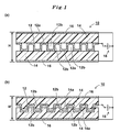
- FIG. 1A shows the basic structure of a gel actuator according to the present invention.
- This gel actuator 10 includes an anode 12 formed on both sides of a concavo-convex surface using a conductive material such as a metal, and a dielectric polymer material disposed on both surfaces of the anode 12 so as to sandwich the anode 12 in the thickness direction. And a cathode 16 that covers the outer surface of the gel layer 14 (the surface opposite to the surface in contact with the anode 12).
- the gel layer 14 is formed in a flat film shape and is stacked so as to straddle the convex portion 12a of the anode 12, and a portion of the concave portion 12b in the middle of the convex portion 12a becomes a void.
- the unit structure that performs the actuator action of the gel actuator includes one gel layer 14, and an anode 12 and a cathode 16 that sandwich the gel layer 14 in the thickness direction. That is, the unit structure is [anode 12, gel layer 14, cathode 16].
- the unit structure is [anode 12, gel layer 14, cathode 16].
- the cathode 16 is electrically short-circuited.
- the basic structure of the gel actuator shown in FIG. 1A is obtained by laminating two unit structures in opposite directions using the anode 12 in common. By arranging in this way, in the basic structure, an electrical short circuit between the two unit structures is avoided.
- the thickness of the actuator is thinner than when the two unit structures are simply laminated in the opposite direction.
- the anode 12 has a waveform shape in which the convex portions 12a and the concave portions 12b are alternately arranged in parallel.
- the anode can be configured in other shapes such as a large number of fine cylinders arranged as convex portions.
- FIG. 2 the external view of the anode 12 of this embodiment is shown.
- the convex portion 12a and the concave portion 12b on one surface side of the anode 12 become the concave portion 12b and the convex portion 12a on the other surface side, and the convex portion 12a and the concave portion 12b have the same shape (the same height, depth and width). ).
- the actuator action of the gel actuator 10 is caused by the action of the gel of the gel layer 14 entering the gap of the recess 12b among the irregularities provided on the surface of the anode 12. Therefore, when considering the actuator action, it is necessary to appropriately set the width, depth, arrangement interval, and the like of the recess 12b formed on the surface of the anode 12.
- the dielectric polymer material contained as a main component in the gel layer 14 is a material that causes bending deformation or creep deformation by applying an electric field. Examples include polyvinyl chloride (PVC), polymethyl methacrylate, polyurethane, polystyrene, polyvinyl acetate, nylon 6, polyvinyl alcohol, polycarbonate, polyethylene terephthalate, polyacrylonitrile, silicone rubber, and the like.
- the gel layer 14 includes a dielectric polymer material and a plasticizer for gelling the dielectric polymer material.
- the gel layer 14 may contain other additives as necessary. When the dielectric polymer material has sufficient deformation characteristics due to an electric field, the gel layer 14 may be formed of only the dielectric polymer material.
- the cathode 16 is for applying a voltage to the gel layer 14 between the anode 12. In order to apply an electric field over the entire surface of the gel layer 14, the cathode 16 is provided so as to cover the entire surface of the gel layer 14. Since the cathode 16 only needs to have a uniform electric field applied to the gel layer 14, the cathode 16 can be formed in a mesh shape without being formed into a complete solid film.
- FIG. 1B shows a state in which a voltage is applied between the anode 12 and the cathode 16.
- a voltage is applied between the anode 12 and the cathode 16
- charges are injected from the cathode 16 into the gel layer 14
- charges are accumulated in the vicinity of the anode 12, the gel creeps, and the gel is formed in the recess 12 b of the anode 12. Get in.
- the gel layer 14 contracts in the thickness direction when the gel enters the gaps of the recesses 12b. That is, the overall thickness H ′ of the gel actuator 10 in FIG. 1B is H ′ ⁇ H with respect to the overall thickness H of the gel actuator 10 in FIG.
- both surfaces of the anode 12 are uneven surfaces, both surfaces of the anode 12 act on the gel layer 14 and have a structure that efficiently contracts as a gel actuator.
- the air gap of the recess 12b may be filled with the gel by the air being pushed out by the gel that enters.
- the gel actuator 10 can be repeatedly contracted by repeatedly performing an operation of turning on and off the voltage applied between the anode 12 and the cathode 16.
- FIG. 3 shows the multilayer structure of the gel actuator. Even if the gel actuator has only a unit structure, it acts as an actuator (contracts-returns in the thickness direction). As shown in FIG. 1, the actuator structure can be doubled by adopting a basic structure in which unit structures are stacked in two layers. As shown in FIG. 3, a larger amount of contraction and generation force can be obtained by laminating a plurality of unit structures that act as actuators.
- the anode 12 is sandwiched between the gel layer 14 and the cathode 16 in the thickness direction.
- the gel layer 14 and the cathode 16 are arranged on both surfaces of the anode 12.
- the anode 16 is laminated on the gel layer 14 provided on both surfaces of the cathode 16.
- the gel layer 14 and the anode 12 are arranged symmetrically with respect to the cathode 16 on both sides sandwiching 16.
- the laminated anode 12 and cathode 16 are connected to the positive electrode and the negative electrode of the power source 18, respectively.
- a plurality of unit structures are stacked in reverse order in order. Adjacent unit structures commonly use the cathode 16 and the anode 12.
- FIG. 4 shows a state in which a voltage is applied to the anode 12 and the cathode 16 of the gel actuator having a laminated structure.
- a voltage By applying a voltage, the gel of the gel layer 14 undergoes creep deformation, and the gel enters the gap in the recess 12b of the anode 12 and contracts in the thickness direction. Since both surfaces of the anode 12 are uneven surfaces, both surfaces of the anode 12 act on the gel layer 14 and have a structure that efficiently contracts as a laminated gel actuator.
- the total amount of shrinkage of the gel actuator formed by alternately laminating the anode 12, the gel layer 14, and the cathode 16 is the sum of the amount of shrinkage of each gel layer 14.
- the amount of shrinkage increases in proportion.
- the force generated by the gel actuator having the laminated structure is also the sum of the force generated based on each gel layer 14. Therefore, in order to obtain a larger contraction amount or actuator force, the number of stacked gel actuators may be increased.
- FIG. 5 shows another configuration example of the stacked gel actuator.
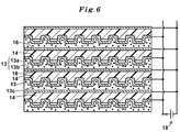
- the gel actuator of the present embodiment is also arranged so that the gel layer 14 is sandwiched between the anode 13 and the cathode 16 in the thickness direction, and the surface of the anode 13 in contact with the gel layer 14 is an uneven surface as in the above-described embodiment. is there.
- both surfaces of the anode 13 are uneven surfaces.
- one surface of the non-conductive base material 13b has an uneven shape, and this uneven surface. Is covered with a conductive layer 13a, and one surface of the anode 13 is an uneven surface.
- the anode can be formed in other shapes such as a large number of fine cylinders arranged as convex portions.
- a component part in which the gel layer 14 is sandwiched between the anode 13 and the cathode 16 is a unit structure that performs an actuator action.
- the stacked gel actuator is configured by stacking a gel layer 14 and a cathode 16 on an anode 13 in this order.
- the anode 13 and the cathode 16 are respectively connected to the positive electrode and the negative electrode of the power source 18 and applied with a voltage.
- a plurality of unit structures are stacked in the same direction, but since the non-conductive base material 13b is provided between adjacent unit structures, an electrical short circuit between the unit structures is avoided. ing.
- FIG. 6 shows a state in which a voltage is applied between the anode 13 and the cathode 16 of the gel actuator shown in FIG.
- the gel of the gel layer 14 is attracted to the convex portion of the anode 13, the gel partially enters the gap of the concave portion 13c of the anode 13, and the gel layer 14 contracts in the thickness direction, The contracting action of the gel actuator occurs.
- the action of the gel layer 14 contracting and returning in response to the operation of turning on and off the voltage application is a reversible action, and can be repeatedly acted on. It can be used as a suitable actuator.
- both surfaces of the anode 12 are uneven, and the gel contraction action is used on both surfaces of the anode 12.
- only one surface of the anode 13 is used for the contraction action of the gel.
- the gel is easily deformed by creep, and the gel enters the recess.
- the base material 13b made of a non-conductive material such as cycloolefin polymer (COP) acts as a support material (support film) for the conductive layer 13a, so that it becomes easy to form a fine pattern.
- COP cycloolefin polymer
- the gel actuator according to the present invention assumes that the thickness of the anode and the gel layer is on the order of ⁇ m.
- the uneven pattern formed on the anode is required to be finely formed with an accuracy of the order of ⁇ m or less.
- various methods are used as a method for forming a fine pattern.
- the formation method of the conventional fine pattern can be utilized. Below, the example of a manufacturing method of a gel actuator is shown.
- FIG. 7 shows an example of manufacturing an anode with both surfaces being uneven.
- corrugated pattern of an anode is formed (FIG.7 (a)).
- a resist pattern is formed on the surface of the substrate 30 so as to cover a portion to be left as a convex portion on the surface of the substrate 30 by photolithography, and the surface of the substrate 30 is etched by using the resist pattern as a protective film.
- a pattern 30a is formed.
- chemical etching or physical etching such as RIE (Reactive Ion Etching) may be selected.
- the concave / convex pattern 30a it is easy to form the concave / convex pattern 30a with an accuracy of several ⁇ m to several tens of ⁇ m.
- a material suitable for forming a fine pattern such as a silicon substrate, a glass plate, or a metal plate is used for the substrate 30.
- FIG. 7B shows a transfer substrate 40 obtained by transferring a concavo-convex pattern from the substrate 30.
- a conductor layer 50 is formed on the surface of the transfer substrate 40 on which the concave / convex pattern 40a is formed (FIG. 7C).
- the conductor layer 50 is provided so as to cover the convex part, concave part, and inner surface of the concave part of the concave / convex pattern 40a so that the concave / convex pattern 40a provided on the transfer substrate 40 is reflected.
- the conductor layer 50 can be formed to a predetermined thickness using a plating method, a sputtering method, or the like. In this embodiment, since both surfaces of the anode are formed in the same shape, the uneven shape of the transfer substrate 40 and the thickness of the conductor layer 50 are controlled so that this waveform is obtained.
- the conductor layer 50 is not limited to being formed as a single layer, but may be provided in a plurality of layers such as a nickel layer as a base material and a surface layer as gold.
- the transfer substrate 40 is chemically dissolved and removed to obtain the anode 12 (FIG. 7D).
- a solvent that can selectively dissolve only the transfer substrate 40 is used. Therefore, it is necessary to select materials for the conductor layer 50 and the transfer substrate 40 so that the transfer substrate 40 can be selectively dissolved and removed.
- the obtained anode 12 is used as a member that is laminated with the gel layer 14 or the like to form a laminated gel actuator.
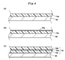
- FIG. 8 shows a manufacturing method of the gel sheet 70 used for manufacturing the gel actuator.
- FIG. 8A shows a state in which the gel layer 14 a is provided on the release sheet 60.
- the gel layer 14a can be formed by coating a gel solution formed by dissolving a dielectric polymer material such as polyvinyl chloride in a solvent and evaporating the solvent.
- the thickness of the gel layer 14a can be controlled to a thickness of about 10 ⁇ m to 100 ⁇ m by a coating method.
- a gel layer is prepared by adding dibutyl adipate (DBA) as a plasticizer, creating a gel solution using tetrahydrofuran (THF) as a solvent, and coating the gel solution.
- DBA dibutyl adipate
- THF tetrahydrofuran
- the plasticizer include DBA, dimethyl adipate (DEA), bisphthalate (BSP), dibutyl phthalate (DBP), and the like.
- the gel layer is the main component of the actuator that contracts by creep deformation, and at the same time, is interposed between the anode and the cathode to provide electrical insulation between the anode and the cathode. It is necessary to form uniformly on the surface of the peeling sheet 60 so that holes and the like are not formed.
- FIG. 8B shows a state in which a conductor layer 16a to be the cathode 16 is formed on the surface of the gel layer 14a.
- the conductor layer 16a can be formed by using a film forming method such as sputtering or plating with a metal such as copper or gold.
- FIG. 8C shows a state in which a gel layer 14b is further formed on the surface of the conductor layer 16a.
- the gel layer 14b can also be formed by a method of coating a gel solution. In this way, the gel sheet 70 in which the gel layers 14 a and 14 b are provided on both surfaces of the conductor layer 16 a is formed on the release sheet 60.
- the stacked gel actuator shown in FIG. 3 can be formed by alternately stacking the anode 12 shown in FIG. 7 and the gel sheet 70 shown in FIG. Since the gel sheet 70 is supported by the release sheet 60, the gel sheet 70 is laminated on the anode 12, and then the release sheet 60 is peeled off to alternately laminate the anode 12 and the gel sheet 70.
- An actuator can be formed. Since the number of layers of the anode 12 and the gel sheet 70 can be set arbitrarily, a gel actuator having an arbitrary number of layers can be obtained by repeatedly selecting the number of layers.
- the gel layer is formed on the release sheet 60 shown in FIG. 8B and the conductor layer 50 formed on the uneven surface of the transfer substrate 40 shown in FIG. What is necessary is just to laminate
- a suitable material constituting the gel actuator is selected as the material of the transfer substrate 40.
- the method for manufacturing the gel actuator is not limited to the embodiment described above.
- a method of forming a concavo-convex pattern on the substrate 30 and transferring the concavo-convex pattern from the substrate 30 to the transfer substrate 40 is not necessarily required.
- the surface of the anode facing the gel layer is an example of a corrugated uneven surface.
- a discrete pattern such as a mesh is formed on the surface of the gel layer. It is also possible to make the gel actuator a laminated structure by using a method of forming a conductor pattern on the substrate.
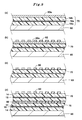
- FIG. 9A shows a state in which a conductor layer 80 a serving as an anode is formed on the surface of the gel sheet 70 supported by the peeling sheet 60.
- the conductor layer 80a can be formed to a predetermined thickness by a plating method, a sputtering method, or the like.
- FIG. 9B shows a state in which a resist pattern 82 is formed by photolithography according to the pattern of the anode 80 to be formed on the surface of the conductor layer 80a.
- FIG. 9C shows a state in which the anode 80 is formed in a predetermined pattern on the surface of the gel sheet 70 by etching the conductor layer 80a using the resist pattern 82 as a protective film and removing the resist pattern 82.
- the gel sheet 70 is newly peeled from the peeling sheet 60 and laminated, and the process of forming the anode 80 on the surface of the laminated gel sheet 70 is repeated to laminate the gel actuator.
- the structure is shown.
- the gel actuator can have any number of layers.
- Electrode connection structure To connect the anode and cathode of a gel actuator with a multilayer structure consisting of an anode, cathode and gel layer to the positive and negative electrodes of the power supply, respectively, connect to the side of the laminate with the anode, cathode and gel layers laminated
- the electrodes can be connected together by providing the electrodes.
- FIG. 10 shows an example in which an anode 12 having a rectangular planar shape, a gel layer 14 and a cathode 16 are laminated to form a gel actuator having a rectangular planar shape, and an electrode 90a and a cathode 16 connected to the anode 12 on the side surface of the laminated body.
- an electrode 90b connected to is provided.
- the anode 12 When the anode 12, the gel layer 14, and the cathode 16 are laminated to connect the electrode 90 a and the anode 12, the anode 12 is extended to one side surface position of the laminate, and the cathode 16 is the other of the laminate. Laminate so as to extend to the side surface position. In this case, one end of the cathode 16 is kept at a position away from one end of the laminate, and the other end of the anode 12 is kept at a position away from the other end of the laminate. To do.
- Electrodes 90a and 90b that electrically connect all the anodes 12 and cathodes 16 of the multilayer body at once are obtained. be able to.
- the gel sheet 70 may be formed such that one end of the cathode 16 is sealed by the gel layer 14 so that one end of the cathode 16 is not exposed at the end of the laminate.
- a method for forming the conductor layer a method using a conductive foil, a conductive film, a conductive paste, a plating method, a sputtering method, or the like can be used.
- a gel actuator having a unit structure composed of an anode, a gel layer, and a cathode, a unit structure thickness of 30 ⁇ m, a number of layers of 1000 layers, a working voltage of 5 V, a generated force of 0.4 MPa, a displacement rate It is possible to obtain a product with 20% and a response of 10 Hz.
- the applied voltage can be reduced to 1/100 and the generated force can be increased 100 times as compared with the conventional gel actuator (unit structure thickness: 3 mm).
- the above specifications are comparable to the generation force, displacement rate, and responsiveness of living muscles, and can be used as actuators in various devices including robot actuators.
- By replacing an actuator such as a conventional motor with this actuator it becomes possible to reduce the size, weight, noise, and flexibility of the device.
- the drive application voltage is reduced, it is easy to ensure safety even when used as an actuator of equipment used in contact with or near the human body. Thereby, application to medical welfare fields, such as a massage device and an assist suit, becomes possible, for example.
- by reducing the thickness of the unit structure it is possible to reduce the size of the gel actuator itself, thereby enabling use as an actuator for a mobile terminal, for example. Furthermore, due to the increase in generated force, it can be applied to large brakes and clutches, etc., which were insufficient with conventional gel actuators.
Landscapes
- Engineering & Computer Science (AREA)
- Manufacturing & Machinery (AREA)
- Physics & Mathematics (AREA)
- Spectroscopy & Molecular Physics (AREA)
- Micromachines (AREA)
Abstract
Description
本発明は前記の課題を解決するためになされたもので、低電圧で生体筋に匹敵する発生力等の特性を有し、小型化を図ることによって、アクチュエータ素子としてさらに広い用途に利用することを可能にするゲルアクチュエータ及びその製造方法を提供することを目的とする。
したがって、陽極と陰極とに挟まれたゲルの厚さを薄くすると、印加する電圧が同一であっても電場(陽極側のゲル表面の電荷密度分布)は増大し、大きなクリープ変形を得ることができる。
図1(a)は、本発明に係るゲルアクチュエータの基本構造を示す。このゲルアクチュエータ10は、金属等の導電材を用いて両面を凹凸面に形成した陽極12と、陽極12を厚さ方向に挟む配置として陽極12の両面に積層して配置した誘電性高分子材料を含むゲル層14と、ゲル層14の外面(陽極12に接する面とは反対側の面)を被覆する陰極16とを備える。
図3は、ゲルアクチュエータの多層構造を示す。ゲルアクチュエータは単位構造のみであっても、アクチュエータ作用(厚さ方向に収縮-復帰する作用)をなす。図1に示すように単位構造を2層に積層した基本構造とすることで、アクチュエータ作用を倍にできる。図3に示すように、アクチュエータ作用をなす単位構造を多数層に積層することにより、より大きな収縮量と発生力を得ることができる。
図5は積層型のゲルアクチュエータの他の構成例を示す。本実施形態のゲルアクチュエータも、陽極13と陰極16とによってゲル層14を厚さ方向に挟む配置とし、ゲル層14に接する陽極13の表面を凹凸面としたことは上述した実施形態と同様である。ただし、上述した実施形態においては、陽極13の両面を凹凸面としたのに対して、本実施形態では、非導電性のベース材13bの一方の面が凹凸形状であり、この凹凸形状の表面を導電層13aにより被覆して、陽極13の片面を凹凸面としている。なお、陽極は、微細な円柱を凸部として多数配置するなど他の形状により構成することも可能である。
積層型のゲルアクチュエータを形成する際に、陽極やゲル層の厚さを薄くすることは積層数を増大させ、かつゲルアクチュエータ全体としてコンパクト化を図る上できわめて重要である。
本発明に係るゲルアクチュエータのように、ゲル層に対向する陽極の表面を凹凸面としてゲル層の収縮作用を利用する場合は、単に陽極やゲル層の厚さを薄くすると、ゲルがクリープ変形して陽極の凹部に入り込んだ際に陽極と陰極とが電気的に短絡するおそれがある。この問題を回避するには、陽極の薄型化を図ると同時に陽極に形成する凹凸パターンを、ゲルがクリープ変形しても陽極と陰極とが短絡しないように層の厚さに応じて設ける必要がある。
電子部品の製造分野等においては、微細パターンを形成する方法として種々の方法がなされている。本発明に係るゲルアクチュエータを製造する場合も、従来の微細パターンの形成方法を利用することができる。以下に、ゲルアクチュエータの製造方法例を示す。
図7に、両面を凹凸面とする陽極の製造例を示す。
まず、陽極の凹凸パターンに合わせて凹凸を形成した基板30を形成する(図7(a))。基板30の表面に、フォトリソグラフィー法により基板30の表面で凸部として残す部位を被覆するレジストパターンを形成し、このレジストパターンを保護膜として基板30の表面をエッチングして基板30の表面に凹凸パターン30aを形成する。基板30に使用する素材に応じて化学的エッチング、あるいはRIE(Reactive Ion Etching)等の物理的エッチングを選択すればよい。フォトリソグラフィー法によれば、数μm~数十μの精度で凹凸パターン30aを形成することは容易である。基板30には、シリコン基板、ガラス板、金属板等の微細パターンの形成に適した素材を用いる。
図7(b)は、基板30から凹凸パターンを転写して得られた転写基板40である。
図8は、ゲルアクチュエータの製造に使用するゲルシート70の製造方法を示す。
図8(a)は、剥離用シート60上にゲル層14aを設けた状態を示す。ゲル層14aは、ポリ塩化ビニル等の誘電性高分子材料を溶媒に溶解して形成したゲル溶液をコーティングし、溶媒を蒸発させることによって形成することができる。ゲル層14aの厚さは、コーティング方法により10μm~100μm程度の厚さに制御することが可能である。
図8(c)は、導体層16aの表面にさらにゲル層14bを形成した状態を示す。ゲル層14bもゲル溶液をコーティングする方法によって形成することができる。
こうして、剥離用シート60上に、導体層16aの両面にゲル層14a、14bを設けたゲルシート70が形成される。
図3に示す積層型のゲルアクチュエータは、図7に示す陽極12と図8に示すゲルシート70とを交互に積層することによって形成することができる。ゲルシート70は剥離用シート60により支持されているから、陽極12にゲルシート70を積層した後、剥離用シート60を剥離することによって、陽極12とゲルシート70とを交互に積層して積層型のゲルアクチュエータを形成することができる。陽極12とゲルシート70との積層数は任意に設定できるから、繰り返し積層数を選択することで任意の積層数のゲルアクチュエータを得ることができる。
ゲルアクチュエータの製造方法は上述した実施形態に限定されるものではない。図7に示す製造工程では、基板30に凹凸パターンを形成し、基板30から転写基板40に凹凸パターンを転写する方法としたが、必ずしもこの方法によらなければならないわけではない。
また、上述した実施形態においては、ゲル層に対向する陽極の表面を波形形状の凹凸面に形成した例であるが、以下に示すように、ゲル層の表面にメッシュ状等の離散的なパターンに導体パターンを形成する方法を利用してゲルアクチュエータを積層構造とすることも可能である。
陽極、陰極、ゲル層からなる多層の積層構造としたゲルアクチュエータの陽極と陰極を、それぞれ電源の正極と負極に接続するには、陽極、陰極、ゲル層を積層した積層体の側面に接続用の電極を設ける方法により、一括して接続することができる。
このゲルアクチュエータは、従来のゲルアクチュエータ(単位構造厚さ3mm)に比べ、印加電圧を100分の1にすることができ、かつ発生力を100倍にすることが可能となる。
12 陽極
12a 凸部
12b 凹部
13 陽極
13a 導電層
13b ベース材
13c 凹部
14、14a、14b ゲル層
16 陰極
16a 導体層
18 電源
30 基板
30a 凹凸パターン
40 転写基板
40a 凹凸パターン
50 導体層
60 剥離用シート
70 ゲルシート
80 陽極
80a 導体層
82 レジストパターン
90a、90b 電極
Claims (8)
- 誘電性高分子材料を含むゲル層と、そのゲル層を厚さ方向に挟む陽極と陰極とからなる単位構造を備えるゲルアクチュエータであって、
前記陽極は、前記ゲル層に対向する面が凹凸面に形成されていて、前記凹凸面の凸部が前記ゲル層に接触して、前記凹凸面の凹部が空隙になっていることを特徴とするゲルアクチュエータ。 - 前記単位構造が、電気的短絡を回避する配置で、複数層に積層されていることを特徴とする請求項1に記載のゲルアクチュエータ。
- 前記陽極の両面に前記ゲル層が設けられ、それぞれのゲル層に前記陰極が積層されて形成されていることを特徴とする請求項2に記載のゲルアクチュエータ。
- 前記陰極の両面に前記ゲル層が設けられ、それぞれのゲル層に前記陽極が積層されて形成されていることを特徴とする請求項2又は3に記載のゲルアクチュエータ。
- 前記陽極が、その陽極の一方の面における前記凸部と前記凹部とを、他方の面における前記凹部と前記凸部とする波形形状に形成され、前記凸部と前記凹部とが同形に形成されていることを特徴とする請求項1~4の何れかに記載のゲルアクチュエータ。
- 前記陽極が、非導電性材からなるベース材の一方の面が凹凸形状に形成されていて、その凹凸形状の表面に導電層が被覆されて形成されていることを特徴とする請求項1~4の何れかに記載のゲルアクチュエータ。
- 誘電性高分子材料を含むゲル層と、そのゲル層を厚さ方向に挟む陽極と陰極とからなる単位構造を備えるゲルアクチュエータの製造方法であって、
前記陽極の前記ゲル層に対向する面を、凹凸面に形成する工程を有することを特徴とするゲルアクチュエータの製造方法。 - 前記陰極の両面に前記ゲル層を設けたゲルシートを形成する工程と、
前記ゲルシートに前記陽極を積層する工程とを、有することを特徴とする請求項7に記載のゲルアクチュエータの製造方法。
Priority Applications (3)
| Application Number | Priority Date | Filing Date | Title |
|---|---|---|---|
| JP2013558691A JP5713417B2 (ja) | 2012-02-14 | 2013-02-12 | ゲルアクチュエータ及びその製造方法 |
| EP13749148.6A EP2819293B1 (en) | 2012-02-14 | 2013-02-12 | Gel actuator and method for producing same |
| US14/378,496 US10096762B2 (en) | 2012-02-14 | 2013-02-12 | Gel actuator and method for producing same |
Applications Claiming Priority (2)
| Application Number | Priority Date | Filing Date | Title |
|---|---|---|---|
| JP2012-029010 | 2012-02-14 | ||
| JP2012029010 | 2012-02-14 |
Publications (1)
| Publication Number | Publication Date |
|---|---|
| WO2013122047A1 true WO2013122047A1 (ja) | 2013-08-22 |
Family
ID=48984157
Family Applications (1)
| Application Number | Title | Priority Date | Filing Date |
|---|---|---|---|
| PCT/JP2013/053249 Ceased WO2013122047A1 (ja) | 2012-02-14 | 2013-02-12 | ゲルアクチュエータ及びその製造方法 |
Country Status (4)
| Country | Link |
|---|---|
| US (1) | US10096762B2 (ja) |
| EP (1) | EP2819293B1 (ja) |
| JP (1) | JP5713417B2 (ja) |
| WO (1) | WO2013122047A1 (ja) |
Cited By (8)
| Publication number | Priority date | Publication date | Assignee | Title |
|---|---|---|---|---|
| JP2015104196A (ja) * | 2013-11-22 | 2015-06-04 | 日本信号株式会社 | 高分子アクチュエータ |
| KR101529606B1 (ko) * | 2014-01-09 | 2015-06-19 | 한국표준과학연구원 | 정전기력 기반의 폴리머 액추에이터를 이용한 촉감제시시스템 및 촉감제공방법 |
| JP2016056863A (ja) * | 2014-09-09 | 2016-04-21 | 国立大学法人信州大学 | ゲルアクチュエータを用いたクラッチ機構 |
| WO2016066734A1 (en) * | 2014-10-31 | 2016-05-06 | Danmarks Tekniske Universitet | Dielectric electroactive polymer comprising an elastomeric film in the form of a gel |
| JP2020184815A (ja) * | 2019-04-26 | 2020-11-12 | 三菱ケミカル株式会社 | ゲルアクチュエータ |
| JPWO2021015202A1 (ja) * | 2019-07-22 | 2021-01-28 | ||
| JP2021132523A (ja) * | 2020-02-20 | 2021-09-09 | トヨタ自動車株式会社 | アクチュエータおよびアクチュエータの製造方法 |
| JPWO2022230707A1 (ja) * | 2021-04-28 | 2022-11-03 |
Families Citing this family (13)
| Publication number | Priority date | Publication date | Assignee | Title |
|---|---|---|---|---|
| JP5288419B2 (ja) * | 2011-02-03 | 2013-09-11 | 国立大学法人信州大学 | ゲルアクチュエータ及びこれに用いるゲル |
| US9724877B2 (en) | 2013-06-23 | 2017-08-08 | Robert A. Flitsch | Methods and apparatus for mobile additive manufacturing of advanced structures and roadways |
| US11707882B2 (en) | 2013-06-23 | 2023-07-25 | Robert A. Flitsch | Methods and apparatus for mobile additive manufacturing of advanced roadway systems |
| US11194306B2 (en) * | 2013-06-23 | 2021-12-07 | Addibots, Llc | Methods and apparatus for mobile additive manufacturing with additive manufacturing arrays |
| US11338505B2 (en) | 2013-06-23 | 2022-05-24 | Robert A. Flitsch | Methods and apparatus for mobile additive manufacturing of advanced roadway systems |
| US11505902B2 (en) | 2015-04-15 | 2022-11-22 | Robert A. Flitsch | Methods, materials and apparatus for mobile additive manufacturing of advanced structures and roadways |
| US12291823B2 (en) | 2015-04-15 | 2025-05-06 | Robert A. Flitsch | Methods, materials and apparatus for mobile additive manufacturing of advanced structures and roadways |
| WO2020036594A1 (en) | 2018-08-14 | 2020-02-20 | Flitsch Robert | Methods and apparatus for mobile additive manufacturing |
| US10975529B2 (en) | 2016-02-17 | 2021-04-13 | Robert A. Flitsch | Methods, materials and apparatus for mobile additive manufacturing of advanced structures and roadways |
| JPWO2019065010A1 (ja) * | 2017-09-28 | 2020-10-01 | 豊田合成株式会社 | エラストマー製圧電素子、及びエラストマー製圧電素子の製造方法 |
| US12522985B2 (en) | 2018-08-14 | 2026-01-13 | Robert A. Flitsch | Methods and apparatus for mobile additive manufacturing |
| JP7431085B2 (ja) * | 2020-03-31 | 2024-02-14 | ニデックインスツルメンツ株式会社 | アクチュエータおよびダンパーユニット |
| WO2024119315A1 (zh) * | 2022-12-05 | 2024-06-13 | 华为技术有限公司 | 驱动器和终端设备 |
Citations (7)
| Publication number | Priority date | Publication date | Assignee | Title |
|---|---|---|---|---|
| JPH0241685A (ja) * | 1988-07-29 | 1990-02-09 | Toyota Central Res & Dev Lab Inc | メカノケミカルアクチュエータ |
| JPH0833361A (ja) * | 1994-07-14 | 1996-02-02 | Yaskawa Electric Corp | 静電アクチュエータ |
| WO2004026758A1 (ja) * | 2002-09-20 | 2004-04-01 | Eamex Corporation | 駆動体及びその製造方法 |
| JP2007118159A (ja) * | 2005-10-31 | 2007-05-17 | Furukawa Electric Co Ltd:The | 高分子アクチュエータ集合体、その製造方法、およびその作動方法 |
| JP2009189220A (ja) * | 2008-02-08 | 2009-08-20 | Furukawa Electric Co Ltd:The | アクチュエータ及びこれを用いたアクチュエータ構造体 |
| JP2009273204A (ja) | 2008-05-02 | 2009-11-19 | Shinshu Univ | 高分子柔軟アクチュエータ |
| JP2010016969A (ja) * | 2008-07-03 | 2010-01-21 | Alps Electric Co Ltd | 高分子アクチュエータ及びその製造方法 |
Family Cites Families (4)
| Publication number | Priority date | Publication date | Assignee | Title |
|---|---|---|---|---|
| DE3585938D1 (de) * | 1984-09-26 | 1992-06-04 | Terumo Corp | Ultraschallwandler und verfahren zur herstellung desselben. |
| US5977685A (en) * | 1996-02-15 | 1999-11-02 | Nitta Corporation | Polyurethane elastomer actuator |
| US7880371B2 (en) | 2006-11-03 | 2011-02-01 | Danfoss A/S | Dielectric composite and a method of manufacturing a dielectric composite |
| JP5247123B2 (ja) * | 2007-11-15 | 2013-07-24 | 豊田合成株式会社 | アクチュエータ |
-
2013
- 2013-02-12 US US14/378,496 patent/US10096762B2/en active Active
- 2013-02-12 JP JP2013558691A patent/JP5713417B2/ja active Active
- 2013-02-12 EP EP13749148.6A patent/EP2819293B1/en active Active
- 2013-02-12 WO PCT/JP2013/053249 patent/WO2013122047A1/ja not_active Ceased
Patent Citations (7)
| Publication number | Priority date | Publication date | Assignee | Title |
|---|---|---|---|---|
| JPH0241685A (ja) * | 1988-07-29 | 1990-02-09 | Toyota Central Res & Dev Lab Inc | メカノケミカルアクチュエータ |
| JPH0833361A (ja) * | 1994-07-14 | 1996-02-02 | Yaskawa Electric Corp | 静電アクチュエータ |
| WO2004026758A1 (ja) * | 2002-09-20 | 2004-04-01 | Eamex Corporation | 駆動体及びその製造方法 |
| JP2007118159A (ja) * | 2005-10-31 | 2007-05-17 | Furukawa Electric Co Ltd:The | 高分子アクチュエータ集合体、その製造方法、およびその作動方法 |
| JP2009189220A (ja) * | 2008-02-08 | 2009-08-20 | Furukawa Electric Co Ltd:The | アクチュエータ及びこれを用いたアクチュエータ構造体 |
| JP2009273204A (ja) | 2008-05-02 | 2009-11-19 | Shinshu Univ | 高分子柔軟アクチュエータ |
| JP2010016969A (ja) * | 2008-07-03 | 2010-01-21 | Alps Electric Co Ltd | 高分子アクチュエータ及びその製造方法 |
Non-Patent Citations (5)
| Title |
|---|
| KATUYA FUJII; TAKAFUMI OGIWARA; TOSHIHIRO HIRAI; KEN KINOSHITA: "Influence of the plasticizer on the creep-deformation of PVC gel", POLYMER PREPRINTS, JAPAN, vol. 55, no. 2, 2006, pages 4557 - 4558 |
| MINORU HASHIMOTO; MINAMI SHIBAGAKI; TOSHIHIRO HIRAI: "Development of a Negative Type Brake Using a Contraction Type PVC Gel Actuator", JOURNAL OF THE ROBOTICS SOCIET) OF JAPAN, vol. 29, no. 8, 2011, pages 667 - 674 |
| MISAKI YAMANO; NAOKI OGAWA; MINORU HASHIMOTO; MIDORI TAKASAKI; TOSHIHIRO HIRAI: "Structure and Characteristics of a Contraction Type PVC Gel Actuator", JOURNAL OF THE ROBOTICS SOCIETY OF JAPAN, vol. 27, no. 7, 2009, pages 718 - 724, XP002700156, DOI: doi:10.7210/jrsj.27.718 |
| NAOKI OGAWA; MINORU HASHIMOTO; MIDORI TAKASAKI; TOSHIHIRO HIRAI: "Characteristics Evaluation of PVC Gel Actuators", THE 2009 IEEE RS INTERNATIONAL CONFERENCE ON INTELLIGENT ROBOTS AND SYSTEMS (IROS2009). ST.LOUIS, USA, 2009, pages 2898 - 2903, XP031580777 |
| See also references of EP2819293A4 |
Cited By (14)
| Publication number | Priority date | Publication date | Assignee | Title |
|---|---|---|---|---|
| JP2015104196A (ja) * | 2013-11-22 | 2015-06-04 | 日本信号株式会社 | 高分子アクチュエータ |
| KR101529606B1 (ko) * | 2014-01-09 | 2015-06-19 | 한국표준과학연구원 | 정전기력 기반의 폴리머 액추에이터를 이용한 촉감제시시스템 및 촉감제공방법 |
| JP2016056863A (ja) * | 2014-09-09 | 2016-04-21 | 国立大学法人信州大学 | ゲルアクチュエータを用いたクラッチ機構 |
| WO2016066734A1 (en) * | 2014-10-31 | 2016-05-06 | Danmarks Tekniske Universitet | Dielectric electroactive polymer comprising an elastomeric film in the form of a gel |
| JP2020184815A (ja) * | 2019-04-26 | 2020-11-12 | 三菱ケミカル株式会社 | ゲルアクチュエータ |
| JP7306046B2 (ja) | 2019-04-26 | 2023-07-11 | 三菱ケミカル株式会社 | ゲルアクチュエータ |
| WO2021015202A1 (ja) * | 2019-07-22 | 2021-01-28 | トヨタ自動車株式会社 | アクチュエータ |
| JP7223304B2 (ja) | 2019-07-22 | 2023-02-16 | トヨタ自動車株式会社 | アクチュエータ |
| JPWO2021015202A1 (ja) * | 2019-07-22 | 2021-01-28 | ||
| US11888413B2 (en) | 2019-07-22 | 2024-01-30 | Toyota Jidosha Kabushiki Kaisha | Actuator |
| JP2021132523A (ja) * | 2020-02-20 | 2021-09-09 | トヨタ自動車株式会社 | アクチュエータおよびアクチュエータの製造方法 |
| JP7579503B2 (ja) | 2020-02-20 | 2024-11-08 | トヨタ自動車株式会社 | アクチュエータおよびアクチュエータの製造方法 |
| JPWO2022230707A1 (ja) * | 2021-04-28 | 2022-11-03 | ||
| JP7612847B2 (ja) | 2021-04-28 | 2025-01-14 | 三井化学株式会社 | 高分子圧電性フィルム素子と、それを用いた蓄電デバイスおよび荷重検知デバイス |
Also Published As
| Publication number | Publication date |
|---|---|
| EP2819293B1 (en) | 2018-06-13 |
| JPWO2013122047A1 (ja) | 2015-05-11 |
| US20150171305A1 (en) | 2015-06-18 |
| EP2819293A4 (en) | 2015-10-28 |
| US10096762B2 (en) | 2018-10-09 |
| EP2819293A1 (en) | 2014-12-31 |
| JP5713417B2 (ja) | 2015-05-07 |
Similar Documents
| Publication | Publication Date | Title |
|---|---|---|
| JP5713417B2 (ja) | ゲルアクチュエータ及びその製造方法 | |
| JP5288419B2 (ja) | ゲルアクチュエータ及びこれに用いるゲル | |
| JP2018005903A (ja) | 局在化された及び/又はカプセル化された触覚アクチュエータ及び要素 | |
| KR100664395B1 (ko) | 수축 변위를 정밀 제어하기 위한 폴리머 액추에이터 및 그제어 방법 | |
| JP3959104B2 (ja) | ポリマーアクチュエータ | |
| CN108638049A (zh) | 一种基于电驱动的PVC-gel柔性机械手 | |
| TW201503437A (zh) | 多層機電轉換器之生產的製程 | |
| CN102474206B (zh) | 平板层叠型导电性高分子致动器 | |
| JP5281322B2 (ja) | 電気的伸縮機構及びアクチュエータ | |
| JP6323948B2 (ja) | アクチュエータ素子及びアクチュエータ | |
| CN203617931U (zh) | 一种摩擦发电机及其组成的摩擦发电机组 | |
| KR102399830B1 (ko) | 전기활성 폴리머 액츄에이터의 제조 방법 | |
| KR101594432B1 (ko) | 폴리이미드 유기 유전층을 포함한 정전기력 기반 작동기 | |
| JP6468646B2 (ja) | 積層型アクチュエータ | |
| CN104157783A (zh) | 用于能量变换器的混合膜 | |
| KR101203176B1 (ko) | 희생기판을 이용한 플라스틱 압전소자 제조방법, 이에 따라 제조된 플라스틱 압전소자 | |
| JP2008211879A (ja) | アクチュエータおよび駆動装置 | |
| CN107665851A (zh) | 元件选取系统 | |
| WO2020140501A1 (zh) | 柔性体及控制其发生形变的方法 | |
| JP5930533B2 (ja) | 高分子アクチュエータ及びその製造方法 | |
| KR100599550B1 (ko) | 전왜 폴리머의 팽창력을 수축력으로 변환하는 다층 폴리머액추에이터 | |
| KR20170081872A (ko) | 롤투롤 공법을 이용한 적층형 전기활성 고분자 구동기의 제조 방법 및 그 제조 방법에 의해 제조된 구동기 | |
| JP7645448B2 (ja) | アクチュエータおよびアクチュエータ装置 | |
| JPH0372684A (ja) | 積層型圧電素子 | |
| JP6338281B2 (ja) | 封止高分子アクチュエータ及びその製造方法 |
Legal Events
| Date | Code | Title | Description |
|---|---|---|---|
| 121 | Ep: the epo has been informed by wipo that ep was designated in this application |
Ref document number: 13749148 Country of ref document: EP Kind code of ref document: A1 |
|
| ENP | Entry into the national phase |
Ref document number: 2013558691 Country of ref document: JP Kind code of ref document: A |
|
| WWE | Wipo information: entry into national phase |
Ref document number: 14378496 Country of ref document: US |
|
| NENP | Non-entry into the national phase |
Ref country code: DE |
|
| WWE | Wipo information: entry into national phase |
Ref document number: 2013749148 Country of ref document: EP |