WO2013122170A1 - マルチディスプレイ装置及び表示モジュール - Google Patents
マルチディスプレイ装置及び表示モジュール Download PDFInfo
- Publication number
- WO2013122170A1 WO2013122170A1 PCT/JP2013/053575 JP2013053575W WO2013122170A1 WO 2013122170 A1 WO2013122170 A1 WO 2013122170A1 JP 2013053575 W JP2013053575 W JP 2013053575W WO 2013122170 A1 WO2013122170 A1 WO 2013122170A1
- Authority
- WO
- WIPO (PCT)
- Prior art keywords
- light
- liquid crystal
- image modulation
- display device
- light source
- Prior art date
- Legal status (The legal status is an assumption and is not a legal conclusion. Google has not performed a legal analysis and makes no representation as to the accuracy of the status listed.)
- Ceased
Links
Images



Classifications
-
- G—PHYSICS
- G06—COMPUTING OR CALCULATING; COUNTING
- G06F—ELECTRIC DIGITAL DATA PROCESSING
- G06F3/00—Input arrangements for transferring data to be processed into a form capable of being handled by the computer; Output arrangements for transferring data from processing unit to output unit, e.g. interface arrangements
- G06F3/14—Digital output to display device ; Cooperation and interconnection of the display device with other functional units
- G06F3/1423—Digital output to display device ; Cooperation and interconnection of the display device with other functional units controlling a plurality of local displays, e.g. CRT and flat panel display
- G06F3/1446—Digital output to display device ; Cooperation and interconnection of the display device with other functional units controlling a plurality of local displays, e.g. CRT and flat panel display display composed of modules, e.g. video walls
-
- H—ELECTRICITY
- H04—ELECTRIC COMMUNICATION TECHNIQUE
- H04N—PICTORIAL COMMUNICATION, e.g. TELEVISION
- H04N9/00—Details of colour television systems
- H04N9/12—Picture reproducers
- H04N9/31—Projection devices for colour picture display, e.g. using electronic spatial light modulators [ESLM]
- H04N9/3141—Constructional details thereof
- H04N9/3147—Multi-projection systems
-
- G—PHYSICS
- G09—EDUCATION; CRYPTOGRAPHY; DISPLAY; ADVERTISING; SEALS
- G09F—DISPLAYING; ADVERTISING; SIGNS; LABELS OR NAME-PLATES; SEALS
- G09F9/00—Indicating arrangements for variable information in which the information is built-up on a support by selection or combination of individual elements
- G09F9/30—Indicating arrangements for variable information in which the information is built-up on a support by selection or combination of individual elements in which the desired character or characters are formed by combining individual elements
-
- G—PHYSICS
- G09—EDUCATION; CRYPTOGRAPHY; DISPLAY; ADVERTISING; SEALS
- G09F—DISPLAYING; ADVERTISING; SIGNS; LABELS OR NAME-PLATES; SEALS
- G09F9/00—Indicating arrangements for variable information in which the information is built-up on a support by selection or combination of individual elements
- G09F9/30—Indicating arrangements for variable information in which the information is built-up on a support by selection or combination of individual elements in which the desired character or characters are formed by combining individual elements
- G09F9/35—Indicating arrangements for variable information in which the information is built-up on a support by selection or combination of individual elements in which the desired character or characters are formed by combining individual elements being liquid crystals
-
- H—ELECTRICITY
- H04—ELECTRIC COMMUNICATION TECHNIQUE
- H04N—PICTORIAL COMMUNICATION, e.g. TELEVISION
- H04N9/00—Details of colour television systems
- H04N9/12—Picture reproducers
Definitions
- the present invention relates to a multi-display device that enables a large screen display by arranging a plurality of liquid crystal modules in a tiling manner.
- Patent Document 1 by using a precise cutting technique in the seam cutting process during the liquid crystal panel manufacturing process, a plurality of liquid crystal panels are brought close to an area close to the pixel interval, thereby making the liquid crystal panel seams less noticeable.
- Technology is disclosed.
- Patent Document 2 discloses a technology that makes a joint portion (seam) of a unit panel inconspicuous by installing a panel made of an organic LED at a joint portion of a plurality of unit panels.
- Patent Document 3 discloses a multi-display device in which the joint between liquid crystal modules is not conspicuous without narrowing the frame area and without using an organic LED at the joint.
- Patent Document 3 as shown in FIG. 11, two displays 1001 and 1001 ′ are arranged, and light emitted from the displays is enlarged by a plurality of erecting image forming means 1002 and 1002 ′.
- a multi-display apparatus is disclosed in which image information is transmitted to the same size and an enlarged image is arranged and projected on a screen 1004 by the enlargement means 1003 and 1003 ′.
- the multi-display device disclosed in Patent Document 3 requires optical elements for the erecting image forming means and the enlarging means, respectively, leading to an increase in cost. In particular, it is difficult to manufacture a large area of the erecting image forming means.
- the present invention has been made in view of the above-mentioned problems, and its object is to provide a good solution that makes the seams between the liquid crystal modules less noticeable with a simple configuration without using a means that leads to an increase in cost.
- An object of the present invention is to provide a multi-display device capable of providing an image feeling.
- a multi-display apparatus is a multi-display apparatus in which a transmission type image modulation element in which a plurality of pixels are arranged in a plane is arranged in parallel and in a tiling arrangement, and the image display surface of the image modulation element A light source unit disposed immediately below the center for irradiating the image modulation element with light; a diffusion element disposed on the opposite side of the image modulation element from the light source unit for diffusing the irradiated light; and the image modulation A light that is disposed between the element and the diffusing element, is emitted from the light source unit, and passes through the image modulation element, and is condensed on the diffusion element at a pitch wider than the pixel pitch of the image modulation element. And an image optical element.
- the multi-display device of the present invention it is possible to make the joint between the image modulation elements inconspicuous with a simple configuration without using a means (such as an erect image forming means) that leads to an increase in cost. It has a remarkable effect that a good resolution can be obtained.
- FIG. 2 is a plan view of the multi display device shown in FIG. 1. It is a schematic sectional drawing of the liquid crystal module which comprises the multi-display apparatus which concerns on Embodiment 2 of this invention. It is a schematic sectional drawing of the multi-display apparatus which concerns on Embodiment 2 of this invention. It is a schematic sectional drawing of the multi-display apparatus which concerns on Embodiment 2 of this invention. It is a schematic sectional drawing of the multi-display apparatus which concerns on Embodiment 3 of this invention. It is a schematic sectional drawing of the multi-display apparatus which concerns on Embodiment 4 of this invention. It is a schematic sectional drawing of the liquid crystal module which comprises the multi-display apparatus shown in FIG.
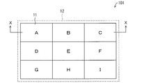
- FIG. 2 shows a plan view of the multi-display device 101 according to the present embodiment.
- the multi-display device 101 realizes a large screen display by arranging a plurality of liquid crystal modules (display modules) 11 in parallel and tiling.
- the liquid crystal module 11 in the tiling arrangement is covered with a diffusion panel 12 (diffusion element) that functions as a screen.
- the images from the respective liquid crystal modules 11 are projected onto the diffusion panel 12, and the images are connected to each other on the diffusion surface of the diffusion panel 12, thereby realizing a large screen display.
- the liquid crystal module 11 has a mechanism that does not cause such a problem.
- FIG. 1 is a cross-sectional view of the multi-display device 101 shown in FIG.
- module A and module B correspond to the reference numerals shown in FIG. Since the modules A and B have the same configuration, the liquid crystal module 11 will be described for convenience of explanation.
- the liquid crystal module 11 includes a liquid crystal panel (image modulation element) 1 and a light source unit 2 including a white LED (W-LED) as a light emitting unit that emits light from the back surface of the liquid crystal panel 1.
- the liquid crystal panel 1 includes a fly-eye lens array (imaging optical element) 3 provided on the light source unit 2 side, supports the liquid crystal panel 1, and does not leak light from the light source unit 2 to the outside.
- a frame portion 5 is provided for this purpose.
- the liquid crystal panel 1 is composed of a light transmission type liquid crystal display element in which a plurality of pixels are arranged in a plane, and controls the transmittance of irradiation light from the light source unit 2 according to the video source.
- the video to be displayed is displayed.
- the liquid crystal panel 1 is not particularly limited as long as it is a light transmission type liquid crystal display element.
- the light source unit 2 is disposed almost directly below the center of the display screen (image display surface) in the liquid crystal module 11 (position just below the center).
- FIG. 1 shows an example in which one white LED is arranged as the light source unit 2, the present invention is not limited to this, and a plurality of white LED light sources can be used as long as it is directly under the center of the display screen. Or an LED light source that emits light having a different main wavelength (for example, each color of RGB) may be disposed.
- the white LED light source may have a shape in which a phosphor emitting yellow is applied on a blue LED chip, or a plurality of phosphors having peaks of multiple wavelengths such as red and green are applied on the blue LED chip. It may be of the shape.
- the organic EL illumination may be disposed directly below the center of the display screen of the liquid crystal module 11, instead of the LED light source.
- the light source unit 2 is arranged at a certain distance from the liquid crystal panel 1 so that the emitted light can be applied to the entire back surface of the liquid crystal panel 1.
- the frame portion 5 described above is necessary to maintain the distance between the liquid crystal panel 1 and the light source portion 2 at an appropriate value.
- the fly-eye lens array 3 is composed of a plurality of lenses 3 a, and each lens 3 a is arranged in a plane at a position corresponding to each pixel pitch of the liquid crystal panel 1 (width of the liquid crystal pixels 6) and close to the liquid crystal panel 1.
- the fly-eye lens array 3 is arranged on the back side of the liquid crystal panel 1, that is, on the light source unit 2 side.
- the lens 3a is a convex lens, and the focal position is adjusted to be the diffusion surface of the diffusion panel 12.
- the diffusion panel 12 has a role of expanding the angle characteristics so that the observer can recognize the light that has passed through the liquid crystal panel 1 from any position, and corresponds to a screen in the projection display device.
- the light emitted from the light source unit 2 passes through the fly-eye lens array 3, so that only the liquid crystal pixels 6 of the corresponding liquid crystal panel 1 are used.
- the light passes through. That is, each pixel information of the liquid crystal panel 1 has only light that has passed through the lens 3 a of the fly-eye lens array 3 corresponding to each liquid crystal pixel 6.
- the liquid crystal panel 1 includes a CF (color filter) panel 4 for color display.
- Each liquid crystal pixel 6 of the liquid crystal panel 1 is composed of different color (RGB) picture elements (R picture element, G picture element, B picture element), and the amount of light passing through each picture element of each liquid crystal pixel 6. By adjusting the color, the color of each pixel can be expressed.
- each liquid crystal pixel 6 of the liquid crystal panel 1 is condensed by the diffusion panel 12 at different locations while each pixel has color information that it wants to express.
- the angle of light incident on the fly-eye lens array 3 from the light source unit 2 is within a maximum of 40 ° with respect to the vertical direction of each lens 3a.
- the emission angle from the light source unit 2 is larger than 40 °, the light beam incident on the fly-eye lens array 3 is deviated from the optical axis direction, and an aberration called field curvature occurs.
- a method of correcting aberrations with a plurality of lens systems is common, but it is not practical from the viewpoint of manufacturing cost.
- the angle of light incident on the fly-eye lens array 3 is within a maximum of 40 ° with respect to the vertical direction of each lens 3a.
- the angle of light incident on the fly-eye lens array 3 is perpendicular to the vertical direction of each lens. More preferably, it is within 30 ° at the maximum.
- the preferable angle of the incident angle of the light beam from the light source unit 2 of each lens 3a of the fly-eye lens array 3 is the same not only in this embodiment but also in each embodiment described later.
- the multi-display device 101 of the present invention since the light rays are condensed using the fly-eye lens array 3, the light passing through the liquid crystal panel 1 is condensed to the front to some extent. Therefore, when the image of the multi-display device 101 is observed at a different viewing angle (from an oblique direction), light does not reach much and the display on the screen becomes difficult to see.
- the diffusion panel 12 is preferably arranged on the opposite side of the liquid crystal panel 1 (image modulation element) from the light source unit 2.
- the diffusion panel 12 further has an incident angle independent diffusion characteristic (a property that the diffusion intensity distribution when passing through the diffusion plate is constant regardless of the incident angle of the incident light to the diffusion element), a different angle. Since the light condensed on the diffusion panel 12 in the distribution has the same diffusion characteristics, the display quality can be improved, which is more preferable.
- incident angle independent diffusion characteristic a property that the diffusion intensity distribution when passing through the diffusion plate is constant regardless of the incident angle of the incident light to the diffusion element
- the diffusion panel 12 Furthermore, in order to achieve higher image quality, it is possible to take measures to suppress backscattering of the diffusion panel 12 disposed on the surface with respect to the external light.
- the light irradiated from the liquid crystal panel 1 side emits diffused light to the viewer side, while the light irradiated to the diffusion panel 12 from the viewer side transmits and diffuses to the liquid crystal panel 1 side. , Reflected and diffused to the viewer side. This reflection action is called backscattering with respect to external light.
- this reflected diffused light is observed together with an image display that has been transmitted through a normal liquid crystal panel 1, the image floats white, leading to a reduction in image quality.
- a method of suppressing backscattering for example, there is a method of disposing a film that absorbs external light in a region where the light that has passed through each liquid crystal pixel 6 is not collected by the diffusion panel 12.
- the film that absorbs the external light suppresses the backscattering of the diffusion panel 12 with respect to the external light, while the light that has passed through each liquid crystal pixel 6 is diffused without being absorbed by the film that absorbs the external light. Can be prevented.
- the circularly polarizing plate is composed of a linear polarizer and a quarter-wave plate.
- each of the quarter-wavelengths in the circularly polarizing plate It is preferable to arrange the plate on the diffusion panel 12 side.
- the structure which provides the said diffusing panel 12, the said diffusing panel 12, and the said circularly-polarizing plate is applicable not only in this Embodiment but in each embodiment mentioned later, and backscattering of external light is carried out.
- the method of suppressing is not limited to the above.
- the light passing through the lens 3a of the fly-eye lens array 3 existing on the leftmost side of the module A passes through the liquid crystal pixel 6 existing on the leftmost side in the liquid crystal panel 1, but at this time, a green (G color) picture is displayed.
- the amount of light passing through the blue (B color) picture element opening is smaller than the light passing through the element opening. This is because the pixel interval from red (R color) to G color, the pixel interval from G color to B color, and the pixel interval from B color to R color are all the same.
- the BM width between the pixels is wider than the BM width between the picture elements.
- the BM width between picture elements indicates a pitch between picture elements. For example, in FIG. 1, the BM width between R and G colors and the BM width between G and B colors in FIG.
- the BM width indicates a pitch between pixels, and corresponds to the BM width between the B color and the R color in FIG.
- the light emitted from the light source unit 2 passes through the fly-eye lens array 3, thereby liquid crystals corresponding to the respective lenses 3 a of the fly-eye lens array 3.
- Light passes through the liquid crystal pixels 6 of the panel 1.
- the angles at which the light emitted from the light source unit 2 is applied to the respective lenses 3a of the fly-eye lens array 3 are different from each other. It is condensed on the diffusion surface.
- the light that has passed through the liquid crystal panel 1 is collected on the diffusion surface of the diffusion panel 12, so that it is within a region that is entirely enlarged than the display screen of one liquid crystal module 11 (the diffusion surface of the diffusion panel 12). Each will be condensed.
- each liquid crystal module 11 is enlarged and applied to the diffusion surface of the diffusion panel 12, which is the outermost surface of the multi-display device 101, so that the frame portion 5 of the liquid crystal module 11 is made thinner than necessary. There is no need to do this, and a large screen display without a seam is possible.
- the module A is assumed as the liquid crystal module 11, but the configuration of the adjacent module B is exactly the same as that of the liquid crystal module 11, and the light that has passed through the liquid crystal panel of the module B is displayed on the display screen. The light is collected in a region that is enlarged as a whole.
- the light from the two modules A and B is diffused in the direction of light by the diffusion panel 12 existing on the same plane. That is, the observer of the multi-display device 101 recognizes the diffusion surface of the outermost diffusion panel 12 instead of the display screens of the modules A and B. In the outermost diffusion panel 12, the light passing through the modules A and B is collected in a region enlarged from the respective display screens.
- the gap between the condensing position of the pixel information corresponding to the outermost periphery of the module A and the condensing position of the pixel information corresponding to the outermost periphery of the module B is substantially equal to the condensing position interval of the pixel information in each module.
- the observer of the multi-display apparatus 101 can recognize an image that has passed through the two modules A and B as one piece of image information.
- the liquid crystal modules 41 can be easily connected with a simple configuration without using any means (such as an upright imaging unit) that leads to an increase in cost. This produces a remarkable effect of making the seam of the screen less noticeable and providing a good resolution.
- the example in which the light source unit 2 of each liquid crystal module 11 is arranged only immediately below the center of the display screen is shown.
- the liquid crystal module 11 becomes large, it is necessary to increase the light emission amount of the light source unit 2 and to increase the distance from the light source unit 2 to the liquid crystal panel 1. Therefore, in the case of the multi-display device 101 shown in the first embodiment, the preferred size of the liquid crystal module 11 is 10 to 15 inches diagonal at the maximum.
- FIG. 3 is a schematic cross-sectional view of the liquid crystal module 21 constituting the multi-display device 201 according to the present embodiment.
- the liquid crystal module 21 is configured by the light source unit 2 having a plurality of blocks 21a arranged in parallel. That is, one liquid crystal module 21 is divided into a plurality of units, and one divided unit is a block 21a, and one light source unit 2 is arranged in the block 21a.
- the light source unit 2 is disposed almost directly below the center of the display screen that the block 21a is in charge of. Since the configuration of the light source unit 2 is the same as that of the first embodiment, description thereof is omitted here.
- the block 21a is described when it is not necessary to distinguish between the blocks. However, when the blocks need to be distinguished, they are described as blocks 1 and 2.
- fly-eye lens array 3 and the diffusion panel 12 which are the other components constituting the block 21a is the same as in the first embodiment, and the description thereof is omitted here.
- the block 21a has substantially the same configuration as the liquid crystal module 11 of the first embodiment.
- the difference from the liquid crystal module 11 of the above embodiment is that the light shielding portion 7 is provided between the blocks 21a.
- the light shielding unit 7 is installed for the purpose of preventing the light from the light source unit 2 of the block 1 from being applied to the fly-eye lens array 3 of the block 2, for example. If the light from the light source unit 2 of the block 1 is applied to the fly eye lens array 3 of the block 2, the light passes through the fly eye lens array 3 and travels to a location different from the position where the light should be condensed. Diffused in. At this time, the light emitted from the light source unit 2 of the block 2 is mixed in color, leading to a reduction in image quality.
- an area not used (black display area) is generated in the display screen of the liquid crystal module 21.
- the display screen of the liquid crystal module 11 and the outer size of the fly-eye lens array 3 are substantially equal, whereas in the second embodiment, the outer size of the fly-eye lens array 3 is
- the size of each block 21a is approximately the same, and the liquid crystal panel 1 is larger than one block. Therefore, a location corresponding to the light shielding portion 7 between the blocks 21a in the liquid crystal panel 1 is a region where no image is displayed. In this area, it is possible to apply a conventional liquid crystal panel as it is by performing black display, and wiring for driving the active matrix of the liquid crystal panel 1 may be spread in an area where the image is not displayed. .
- FIG. 4 is a schematic cross-sectional view of a multi-display device 201 in which the liquid crystal modules 21 shown in FIG.
- the multi-display device 201 has one liquid crystal module 21 arranged in parallel and in a tiling arrangement while realizing the inside of one liquid crystal module 21 with the configuration shown in FIG. A large screen display larger than that of the module 21 can be displayed as an integral image seamlessly.
- a great advantage is a reduction in the thickness of the multi-display device 201.
- the distance from the liquid crystal panel 1 to the light source unit 2 needs to be at least 400 mm apart.
- the distance from the panel 1 to the light source unit 2 may be longer than at least 45 mm. Therefore, it is possible to realize a large screen display more compactly by arranging the liquid crystal modules 21 described in the present embodiment in parallel rather than applying the liquid crystal module 11 described in the first embodiment. Become.
- FIG. 3 shows an example in which the fly-eye lens array 3 is used for each of the block 1 and the block 2, one large fly-eye lens may be used. That is, it is not necessary for the block size and the fly-eye lens size to coincide with each other, and it is desirable to manufacture the fly-eye lens with a size that can maximize the manufacturing cost merit.
- the light shielding unit 7 (or the liquid crystal panel 1).
- a light shielding region (not shown) is provided, the above configuration is unnecessary if all the light from the light source unit 2 is irradiated only in the corresponding block 21a.
- the image display corresponding to the light shielding area is all black.
- the number of pixels displayed on the diffusion panel 12 decreases with respect to the total number of pixels of the plurality of liquid crystal modules, but the current liquid crystal module can be diverted.
- the light shielding member in the liquid crystal panel 1 includes a wiring member such as a TFT, a BM (black mask) of a color filter, and a member for maintaining a liquid crystal interlayer thickness (a photo spacer used in a current liquid crystal display).
- a wiring member such as a TFT, a BM (black mask) of a color filter, and a member for maintaining a liquid crystal interlayer thickness (a photo spacer used in a current liquid crystal display).
- One of these members may be used, or a plurality of members may be combined (laminated). This makes it possible to match the number of pixels displayed on the diffusion panel 12 with the total number of pixels of the plurality of liquid crystal modules.
- the light that has passed through the liquid crystal panel 1 is collected on the diffusion surface of the diffusion panel 12, and therefore, within the area that is enlarged as a whole than the size of one block 21 a constituting the liquid crystal module 21 (the diffusion panel 12 The light is condensed on the respective diffusion surfaces.
- each pixel information of the liquid crystal panel 1 has only light that has passed through the lens 3 a of the fly-eye lens array 3 corresponding to each liquid crystal pixel 6.
- Each pixel of the liquid crystal panel 1 is composed of a plurality of picture elements (R picture element, G picture element, B picture element) each having a color filter (CF panel 4) of a different color, and each picture of each pixel. It is possible to express the color of each pixel by adjusting the amount of light passing through the element.
- each liquid crystal pixel 6 of the liquid crystal panel 1 is condensed by the diffusion panel 12 while having color information that each pixel wants to express.
- the direction of the light from the two blocks 1 and 2 is diffused by the diffusion panel 12 existing on the same plane. That is, the observer of the multi-display device 201 recognizes not the display screen of each liquid crystal module 21 but the diffusion surface of the outermost diffusion panel 12. In the outermost diffusion panel 12, the light passing through the modules A and B is collected in a region enlarged from the respective display screens.
- the gap between the condensing position of the pixel information corresponding to the outermost periphery of the block 1 and the condensing position of the pixel information corresponding to the outermost periphery of the block 2 is considered to be substantially equal to the condensing position gap of the pixel information of each block.
- the observer of the multi-display device 201 can recognize an image that has passed through two blocks as one piece of image information.
- each piece of pixel information is condensed at almost one point, an image with high resolution can be displayed.
- each module A, B, C is composed of three blocks, and that the interval between the blocks is substantially equal to the condensing position interval of each pixel information as described above.
- the gap between the light collection position of the pixel information corresponding to the outermost periphery of the right block of the module A and the light collection position of the pixel information corresponding to the outermost periphery of the left block of the module B is considered to be substantially equal to the light collection position of each image information.
- the observer of the multi-display device 201 can recognize an image that has passed through the two modules A and B as one piece of image information. If the same condition can be established between the module B and the liquid crystal module C, it becomes possible for the observer to recognize a larger image as one piece of image information. Display is possible.
- FIG. 5 is a schematic cross-sectional view of the liquid crystal module 31 constituting the multi-display device 301 according to the present embodiment.
- the light source unit 32 is disposed almost directly below the center of the display screen of the liquid crystal panel 1, as in the liquid crystal module 11 of the first embodiment.
- the light source unit 32 is composed of LED light sources that emit RGB colors. These LED light sources are arranged with a space therebetween. By doing so, the light emitted from each color LED is irradiated to the fly-eye lens array 3 at different angles.
- each lens 3 a of the fly-eye lens array 3 is set so as to be located on the diffusion surface of the diffusion panel 12.
- the liquid crystal panel 1 is arranged at a height at which light emitted from each color LED after passing through each lens 3a of the fly-eye lens array 3 passes through spatially different positions. By doing so, it becomes possible to pass only the light of the corresponding color into each picture element constituting the liquid crystal pixel 6 of the liquid crystal panel 1, and it is possible to remove the color filter which causes a large light loss. It becomes.
- the diffusion panel 12 has a role of expanding the angle characteristics so that the observer can recognize the light that has passed through the liquid crystal panel 1 from any position, and corresponds to a screen in the projection display device.
- the light of the light source unit 2 is passed through the pixels of the respective liquid crystal panels corresponding to the respective lens arrays.
- light of different colors from the light source unit 32 is allowed to pass through the pixels of the respective colors constituting the liquid crystal pixels 6 of the respective liquid crystal panels 1 corresponding to the respective lens arrays.
- the light emitted from the light sources of RGB colors in the light source unit 32 is irradiated to the fly-eye lens array 3 at different angles. It is condensed toward Immediately after the lens 3a of the fly-eye lens array 3, the light emitted from the light sources of RGB colors exists in the same plane. To go through.
- the pixel region of the liquid crystal panel 1 is arranged at a height at which the light of each RGB color passes through different planes. It is possible to pass light.
- the focal position of the fly-eye lens array 3 is set to the diffusion position of the diffusion panel 12, the light that has passed through each picture element constituting the liquid crystal pixel 6 is condensed at different positions on the diffusion panel 12. In addition, the light is condensed in a region enlarged as a whole than the liquid crystal module.
- the multi-display device 301 when configured by arranging a plurality of similar liquid crystal modules in parallel, the observer can recognize it as one large image information without a joint, and at the same time, the observer can recognize the multi-display. Even when viewed close to the apparatus 301, the pixel information can be visually recognized without mixing colors, so that a display with high resolving power can be realized.
- the resolving power is an index of whether or not the image looks clear when the observer looks at the screen. The higher the resolving power, the clearer the image.
- the difference between the case of the first and second embodiments and the case of the present embodiment is whether the light reaching the diffusion panel 12 is condensed for each pixel information or for each pixel information. Although it has occurred, in fact, these resolving powers are almost the same level.
- both the first and second embodiments in the case of the present embodiment, when viewed in units of pixels, a region where light does not reach between adjacent pixel information in the diffusion panel 12 is generated. Pixel information to be processed is never mixed. Therefore, both the first and second embodiments and the present embodiment can display an image with high resolving power. In a large screen display system in which a simple projection system is tiled, it can be said that the present application is more advantageous in terms of resolution.
- the multi-display device 301 when attention is focused on the light collected at each position of the diffusion panel 12, the light emitted from the light source unit 32 corresponds to each by passing through the fly-eye lens array 3.
- the light passes through the picture elements constituting the liquid crystal pixel 6 of the liquid crystal panel 1. That is, each picture element information of the liquid crystal panel 1 has only light that has passed through each picture element. Therefore, even in the case where each pixel of the liquid crystal panel 1 is not provided with a color filter, it is possible to express the color of each pixel by adjusting the amount of light passing through each pixel. It is possible to display full color without using it.
- the integrated image is displayed without making the joint of the liquid crystal module visible to the observer, and the light loss absorbed by the color filter is greatly reduced. By reducing the power consumption, it is possible to realize low power consumption.
- the contents described above have been described for the module A. However, the same applies to the adjacent module B, and the light that has passed through the liquid crystal panel of the module B is in an area that is enlarged as a whole than the display screen (the diffusion panel 12). Are respectively condensed on the diffusion surface).
- the direction of the light from the two modules A and B is diffused by the diffusion panel 12 existing on the same plane. That is, the observer of the multi-display device 301 recognizes the diffusion surface of the outermost diffusion panel 12 instead of the display screens of the joules A and B. In the diffusing panel 12 on the outermost surface, the light passing through the modules A and B is collected in a region enlarged from the respective display screens.
- the gap between the condensing position of the pixel information corresponding to the outermost periphery of the module A and the condensing position of the pixel information corresponding to the outermost periphery of the module B is substantially equal to the condensing position interval of the pixel information in each module.
- the observer of the multi-display device 301 can recognize an image that has passed through the two modules A and B as one piece of image information.
- each piece of pixel information is condensed at almost one point, an image with high resolution can be displayed.
- one liquid crystal module may be divided into a plurality of blocks, and the light source unit 32 may be arranged in each block.
- the thickness of the multi-display device 301 it is possible to reduce the thickness of the multi-display device 301 by focusing the picture element information on the diffusion panel 12 with light passing through each block at substantially equal intervals.
- the multi-display device 301 that does not need to be provided with a color filter has been described.
- the presence or absence of a color filter is examined.
- each of the picture elements constituting the liquid crystal pixel 6 that is a light transmitting portion corresponds to each of R, G, and B to which each picture element corresponds. Only light emitted from the LED (light source unit 32) passes therethrough. In this state, the liquid crystal panel 1 corresponding to each picture element is driven by an applied voltage through a driving element, so that it is possible to ideally perform full color display without a color filter.
- FIG. 6 is a schematic cross-sectional view of the liquid crystal module 41 constituting the multi-display device 401 according to the present embodiment.
- the fly-eye lens array 3 is set so that the focal position of each lens 3a is the position of the diffusion surface of the diffusion panel 12. Details of the pitch of the lenses 3a of the fly-eye lens array 3 will be described later.
- the liquid crystal panel 1 is arranged at a height at which the light passing through each liquid crystal pixel 6 passes through spatially different positions. By doing so, the light passing through each liquid crystal pixel 6 of the liquid crystal panel 1 can be condensed at different locations by the diffusion panel 12.
- the diffusion panel 12 has a role of expanding the angle characteristics so that the observer can recognize the light that has passed through the liquid crystal panel 1 from any position, and corresponds to a screen in the projection display device.
- the fly-eye lens array 3 is applied to the liquid crystal pixels 6 (or picture elements) of one liquid crystal panel 1.
- the light from one lens 3a is condensed by the diffusion panel 12, and in this embodiment, the fly-eye lens array 3 is applied to the liquid crystal pixels 6 of one liquid crystal panel 1.
- the light from the two lenses 3a is allowed to pass through and the light is condensed at one point by the diffusion panel 12.
- the pitch P1 between the two light source sections 2, the pitch P2 between the lenses 3a of the fly-eye lens array 3, and the light collection pitch P3 of the diffusion panel 12 are shown in FIG. May be arranged so as to satisfy the above condition.
- 7a is the distance from the light source unit 2 to the fly-eye lens array 3
- b is the distance from the fly-eye lens array 3 to the diffusion panel 12
- n is the reduction magnification of the fly-eye lens array 3. This is a calculated value.
- a and b have all shown the length at the time of converting into the refractive index of air. 1 / n is the imaging magnification of the fly-eye lens array 3.
- the logical description of the light having passed through the plurality of lenses 3a of the fly-eye lens array 3 having the above-described configuration collected at one point by the diffusion panel 12 will be described later.
- the important point in the present embodiment is the liquid crystal panel. 1 arrangement.
- the light emitted from the light source unit 2 at different positions is irradiated to the lenses 3a of the fly-eye lens array 3 at different angles.
- a certain plane dotted circle Y in the lens array in FIG. 7
- dotted circle Z near the liquid crystal panel in FIG. 7
- liquid crystal panel 1 is arranged at a height at which the dotted circle Y in the lens array in FIG. 7 exists, light having a plurality of angular distributions in different principal ray directions with respect to one liquid crystal pixel 6 is obtained.
- the light reaches the different positions in the diffusion panel 12 and is diffused. That is, one piece of pixel information is present at a different position, resulting in color mixing with adjacent pixel information, resulting in a decrease in resolution.
- the light that has passed through the liquid crystal panel 1 is condensed in a region that is larger than the module A. Therefore, when a plurality of similar modules are arranged in parallel, the observer is It can be recognized as one large image information without a joint.
- FIG. 8 is a schematic diagram for mathematically explaining light passing through each lens 3a of the fly-eye lens array 3 from the light source unit 2 which is the white light source of FIG.
- the white light source (light source unit 2) in FIG. 8 are L1 and L2
- the centers of the lenses 3a of the fly-eye lens array 3 are M1 and M2
- the condensing positions on the diffusion panel 12 are P1 and P2. .
- Line M1M2 Line L1M1 x Line P1P2 / Line L1P1 (2)
- line P1P2 P
- the line M1M2 is calculated as n ⁇ P / (n + 1). Therefore, when the line M1M2 that is the lens pitch of the lenses 3a of the fly-eye lens array 3 is n ⁇ P / (n + 1), the light from the white light source can be condensed at different positions of the diffusing element. .
- Line L1L2 / Line L1P1 Line M1M2 / Line M1P1 (3) Since the pitch between the white light sources corresponds to the line L1L2, it is derived from the following relational expression (4) from the above expression (3).
- Line L1L2 Line L1P1 x Line M1M2 / Line M1P1 (4)
- the line M1P1 b
- the line L1L2 Calculated as n ⁇ P. Therefore, when the line L1L2 that is the pitch between the white light sources is n ⁇ P, the light from the plurality of white light sources can be condensed at one place in the diffusing element.
- one liquid crystal module may be divided into a plurality of blocks, and two light source units 2 may be arranged in each block.
- the multi-display device 401 can be thinned.
- the configuration of the present embodiment can also be applied to the configuration of the third embodiment. That is, a plurality of RGB-LED light sources are used as the light source unit, the LED light sources, the pitch of the lenses 3a of the fly-eye lens array 3, and the light collection position of the diffusion panel 12 are arranged at appropriate intervals, and the liquid crystal panel 1
- the light emitted from the light source unit 2 passes through the plurality of lenses 3a of the fly-eye lens array 3 by adjusting the height of the liquid crystal panel 6 to a predetermined position. Light passes through the element. From this, as in the third embodiment, it is possible to reduce the power consumption, and it is possible to improve the display image quality by averaging the LED individual difference variation of each RGB color.
- FIG. 9 is a schematic cross-sectional view of the multi-display device 501 according to the present embodiment.
- the large difference between the multi-display device 501 and the multi-display devices 101 to 401 described in the first to fourth embodiments is that the diffusion panel 52 corresponding to the screen is not flat as shown in FIG. In other words, it is a curved surface, and the characteristics of each lens 3a of the fly-eye lens array 3 for condensing light on the diffusion panel 52 are changed depending on the location.
- the light source unit 2 is disposed almost directly below the center of the display screen of the liquid crystal panel 1, as in the liquid crystal module 11 of the first embodiment.
- a white LED is used as in the first embodiment. Since the description of the light source unit 2 is the same as that of the first embodiment, the description thereof is omitted here.
- the fly-eye lens array 3 is arranged in a plane at an interval corresponding to the pixel pitch of each liquid crystal pixel 6 of the liquid crystal panel 1 and at a position close to the liquid crystal panel 1.
- each lens 3 a of the fly-eye lens array 3 is the height from the lens surface of the lens 3 a to the diffusion position of the diffusion panel 52.
- the pitch and focus position of each lens 3a of the fly-eye lens array 3 may not be the same, and may be changed as necessary.
- the focal position of the lens 3a of the fly-eye lens array 3 is preferably changed by each lens 3a so that it becomes the diffusion position of the diffusion panel 52.
- the diffusion panel 52 has a function of expanding the angle characteristics so that the observer can recognize the light that has passed through the liquid crystal panel 1 from any position, and corresponds to a screen of a projection display device. Therefore, as in the present embodiment, the diffusion panel 52 may be a curved surface instead of a flat surface.
- the present embodiment and the first to fourth embodiments are largely different from each other, as described above, the diffusion panel 52 corresponding to the screen is not a flat surface but a curved surface having a curvature, and condenses light on the diffusion panel 52.
- the characteristic of each lens 3a of the fly-eye lens array 3 is changed depending on the place.
- the light emitted from the light source unit 2 passes through the fly-eye lens array 3, thereby passing through the liquid crystal pixels 6 of the liquid crystal panel 1 corresponding to the respective lenses 3 a of the fly-eye lens array 3.
- Light passes through.
- the angles at which the light emitted from the light source unit 2 is applied to the respective lenses 3a of the fly-eye lens array 3 are different, and the light after passing through the fly-eye lens array 3 is also collected along different principal ray directions.
- the light that has passed through the liquid crystal panel is condensed by the diffusing element, and is condensed in a region that is enlarged as a whole than the display screen of the liquid crystal module.
- the multi-display device 501 having the above-described configuration even if the diffusion panel 52 is a curved surface, it is possible to maintain a good light collection state at any location of the diffusion panel 52 and display an image with high resolution. Become.
- the multi-display device 501 when attention is focused on the light collected at each position of the diffusion panel 52, the light emitted from the light source unit 2 passes through each lens 3a of the fly-eye lens array 3. Thus, light passes through the corresponding pixels of the liquid crystal panel 1.
- the liquid crystal panel 1 by adjusting the amount of light passing through each picture element of each liquid crystal pixel 6, each image information is given to the pixel transmitted light and condensed on the diffusion panel 52.
- the diffusing element is a curved surface, by changing the lens characteristics of the respective lenses 3a of the fly-eye lens array 3, a good condensing state can be realized at any place. .
- the light that has passed through the liquid crystal panel 1 of the liquid crystal module 51 is condensed in a region that is enlarged as a whole than the display screen.
- the two modules A and B do not need to be arranged on the same plane, and are preferably arranged to be inclined as necessary. Therefore, the frame part 5 of each module A, B does not need to be perpendicular to the plane on which the light source part 2 is arranged, and is preferably provided with an inclination if necessary.
- the liquid crystal panel 1 that modulates an image can be realized as a flat surface while the diffusion panel 52 visually recognized by the observer is a curved surface.
- the diffusion panel 52 has a curved surface that swells toward the viewer with respect to the liquid crystal module 51, but conversely, it may have a curved surface that is recessed toward the liquid crystal module 51. Even in this case, it is possible to realize a good light-collecting state by changing the lens characteristics of each lens 3a of the fly-eye lens array 3.
- FIG. 10 is a schematic cross-sectional view of the multi-display device 601 according to the present embodiment.
- the multi-display device 601 is configured by arranging a plurality of liquid crystal modules 61 in parallel as in the multi-display device 101 of the first embodiment.
- the liquid crystal module 61 has substantially the same configuration as the liquid crystal module 11 described in the first embodiment, but is largely different in that a Fresnel lens 62 is provided on the light incident surface side of the diffusion panel 12.
- the liquid crystal module 61 having the above configuration has a Fresnel lens 62 in the vicinity of the light incident surface side of the diffusion panel 12, and the focal position of the Fresnel lens 62 is in the vicinity of the light source unit 2.
- each lens 3 a of the fly-eye lens array 3 provided in the liquid crystal module 61 has a pitch wider than the arrangement pitch of the liquid crystal pixels 6 of the liquid crystal panel 1 by using the light emitted from the light source unit 2 on the Fresnel lens 62. It is supposed to be condensed with.
- the angular distribution of light passing through each pixel of the liquid crystal panel 1 differs depending on the position reaching the diffusion panel 12.
- the Fresnel lens 62 when the Fresnel lens 62 is added as in the present embodiment, the light passing through each liquid crystal pixel 6 of the liquid crystal panel 1 passes through the Fresnel lens 62 because the focal position of the Fresnel lens 62 is the light source unit 2. Later, it reaches the diffusion panel 12 with substantially the same angular distribution. For this reason, it is possible to easily match the diffusion angle characteristics of the pixel information, and the observer of the multi-display device 601 has a remarkable effect that a good image can be viewed from any angle.
- a multi-display apparatus is a multi-display apparatus in which a transmission type image modulation element in which a plurality of pixels are arranged in a plane is arranged in parallel and in a tiling arrangement, and the image display surface of the image modulation element A light source unit disposed immediately below the center for irradiating the image modulation element with light; a diffusion element disposed on the opposite side of the image modulation element from the light source unit for diffusing the irradiated light; and the image modulation A light that is disposed between the element and the diffusing element, is emitted from the light source unit, and passes through the image modulation element, and is condensed on the diffusion element at a pitch wider than the pixel pitch of the image modulation element. And an image optical element.
- the direction of the light from each image modulation element is diffused by the diffusion element existing on the same plane. That is, the observer of the multi-display apparatus recognizes not the display screen of each image modulation element but the diffusion surface of the diffusion element that is the outermost surface of the multi-display apparatus.
- the light emitted from the light source unit disposed at a position immediately below the center of the image display surface of the image modulation element by the imaging optical element and transmitted through the image modulation element is wider than the pixel pitch of the image modulation element.
- the display screen formed on the diffusion element is enlarged as a whole than the display screen of the image modulation element.
- the gap between the pixel information condensing position corresponding to the outermost periphery of the image modulation element and the light condensing position of pixel information corresponding to the outermost periphery of another image modulation element adjacent to the image modulation element is
- the observer of the multi-display device can recognize the image that has passed through the two image modulation elements as one image information. It becomes.
- each image modulation element is condensed at almost one point on the diffusion surface of the diffusion element by the imaging optical element, an image with high resolution can be displayed.
- the multi-display device having the above-described configuration, it is possible to reduce the cost between the image modulation elements with a simple configuration without using a means (such as an erecting imaging means) that leads to an increase in cost.
- a means such as an erecting imaging means
- the image modulation element includes a plurality of pixels arranged at a predetermined pitch, each pixel includes a plurality of picture elements corresponding to each color, and the imaging optical element has a predetermined lens.
- the lens has a plurality of lens arrays arranged at a pitch, and the lens condenses the light emitted from the light source unit on the diffusion element at a pitch wider than the pixel arrangement pitch of the image modulation element. It is characterized by letting.
- the lens has a lens array in which a plurality of lenses are arranged at a predetermined pitch, and the lens emits light emitted from the light source unit with respect to the diffusion element and is a pixel of the image modulation element.
- the image is enlarged as a whole than the display screen of one image modulation element and is condensed on the diffusion surface of the diffusion element to display a color image.
- the display screen of each image modulation element is enlarged and irradiated on the diffusion surface of the diffusion element, which is the outermost surface in the multi-display device, so a gap existing between adjacent image modulation elements is necessary. There is no need to make it narrower than this, and a large screen display without a seam is possible.
- each image modulation element is condensed at almost one point on the diffusion surface of the diffusion element by the imaging optical element, color mixing between adjacent image modulation elements is eliminated, so that the resolution is high. A color image can be displayed.
- the light source unit includes a light emitting unit that emits light having different main wavelengths
- the image modulation element includes a plurality of pixels arranged at a predetermined pitch, and each pixel includes a plurality of picture elements corresponding to each color.
- the imaging optical element has a lens array in which a plurality of lenses are arranged at a predetermined pitch, and the lens separates the light emitted from the light emitting unit according to color. The separated light is allowed to pass through the picture elements constituting the pixels of the corresponding image modulation element, and is condensed on the diffusion element at a pitch wider than the arrangement pitch of the pixels.
- the light emitted from the light emitting units that emit light having different main wavelengths passes through the lens array, so that the light passes through the pixels constituting the pixels of the corresponding image modulation elements.
- the color of each pixel can be expressed, and full color display can be performed without using a color filter.
- an integrated image can be displayed without causing the observer to visually recognize the joint of the image modulation elements, and the light loss absorbed by the color filter can be greatly reduced. As a result, it is possible to realize low power consumption.
- the image modulation element is divided into a plurality of blocks, the light source unit is arranged at a position directly below the center of the area corresponding to each block of the display screen of the image modulation element, and the image modulation element
- Each pixel includes a plurality of pixels arranged at a pitch, each pixel includes a plurality of pixels corresponding to each color, and the imaging optical element includes a plurality of lenses arranged at a predetermined pitch.
- a lens array wherein the lens condenses the light emitted from the light source unit on the diffusion element, and condenses the light at a pitch wider than the arrangement pitch of the pixels of the image modulation element. Yes.
- the light emitted from the light source unit passes through the lens array, so that the light passes through the pixels of the image modulation element corresponding to each lens of the lens array.
- the angles at which the light emitted from the light source unit is applied to the respective lenses of the lens array are different, and the light after passing through the lenses is also condensed on the diffusion surface of the diffusing element along different principal ray directions. .
- the light that has passed through the image modulation element is collected on the diffusion surface of the diffusion element, it is enlarged as a whole than the size of one block that constitutes the image modulation element and collected on the diffusion surface of the diffusion element. It will be lighted.
- the image modulation elements that are not divided into the plurality of blocks are arranged more than in the case where the image modulation elements are arranged in parallel and tiling. Since the distance between the light source unit and the light source unit can be shortened, the multi-display device can be thinned.
- the image modulation element does not transmit light in a region corresponding to the space between the blocks.
- the light from the light source unit corresponding to one block is prevented from being irradiated to an adjacent block by preventing the image modulation element from transmitting light in a region corresponding to the space between the blocks. Can do.
- the diffusing element is reduced with respect to the total number of pixels of the plurality of image modulation elements, it is possible to divert the existing liquid crystal module as the image modulation element.
- one or more of the members constituting the TFT, the black mask layer of the color filter, and the member for maintaining the liquid crystal interlayer thickness are laminated. Is preferred.
- one or a plurality of members constituting the TFT, the black mask layer of the color filter, and the member for maintaining the liquid crystal interlayer thickness are provided in a region corresponding to the image modulation element between the blocks. By being laminated, it is possible to prevent the light from the light source unit corresponding to one block from being irradiated to adjacent blocks.
- the pitch between each pixel is wider than the pitch between picture elements constituting the pixel.
- the image modulation element passes through the lens of the lens array existing on the leftmost side of the image modulation element because the pitch between the pixels is wider than the pitch between the picture elements constituting the pixel.
- the pitch between the pixels is wider than the pitch between the picture elements constituting the pixel.
- a predetermined pitch for condensing on the diffusing element is P
- an imaging magnification of the imaging optical element is (1 / n)
- the same color pitch P1 of the light source unit is P1 ⁇ n ⁇ P
- the lens pitch P2 of the lens array of the imaging optical element is P2 ⁇ (n / (n + 1)) ⁇ P.
- the diffusing element is configured by arranging a plurality of sheet-like elements having end faces in a region where light is not condensed.
- the diffusing element corresponding to the outermost screen must be uniform in all display areas. That is, for example, in the case of configuring a large screen display device having a diagonal size of 120 inches, the diffusing element needs to have a size of 120 inches diagonal and the manufacturing cost becomes enormous.
- pixel information (or picture element information) is collected separately on the diffusion element corresponding to the screen, and there is a region where light does not reach between the condensing points. To do. Even if there is an end face of the diffusing element in a region where the light does not reach, the light from the image modulation element side is not affected at all, and does not affect the image display quality.
- the diffusion element can be realized by arranging, for example, 6 ⁇ 6 pieces of a diagonal size of 20 inches in parallel, which greatly increases the manufacturing cost of the diffusion element compared to the above. It is expected to be suppressed.
- the focal length of the imaging optical element is changed according to the distance from the imaging optical element to the diffusion element.
- the degree of freedom of the shape of the diffusing element is increased by changing the focal length of the imaging optical element according to the distance from the imaging optical element to the diffusing element. That is, even if the diffusing element is formed on a curved surface, it is possible to appropriately collect image information on the diffusing surface of the diffusing element.
- the diffusion element that the observer visually recognizes is a curved surface, but the image modulation element portion that modulates the image can be realized in a plane. As a result, an increase in the manufacturing cost of an extreme image modulation element can be suppressed, and a flexible multi-display device can be realized.
- the diffusing element is a flat surface or a curved surface having a curvature.
- the image modulation element portion that modulates an image can be realized in a plane regardless of the shape of the diffusion element, an increase in the manufacturing cost of the extreme image modulation element is suppressed, and a flexible multi-display device is provided. Can be realized.
- Each lens of the lens array preferably collects the light emitted from the light source unit on the Fresnel lens at a pitch wider than the arrangement pitch of the pixels of the image modulation element.
- the angular distribution of light passing through each pixel of the image modulation element differs depending on the position reaching the diffusion element.
- a Fresnel lens is added, since the focal position of the Fresnel lens is near the light source section, the light passing through each pixel of the image modulation element has almost the same angular distribution after passing through the Fresnel lens and reaches the diffusion element. To do. Therefore, it is possible to easily match the diffusion angle characteristics of the pixel information, and the observer of the multi-display device can visually recognize a good image from any angle.
- the display module of the present invention is arranged in a transmissive image modulation element in which a plurality of pixels are arranged in a plane, and a position immediately below the center of the image display surface of the image modulation element, and irradiates the image modulation element with light.
- an imaging optical element for condensing the emitted light transmitted through the image modulation element onto the diffusion element at a pitch wider than the pixel pitch of the image modulation element.
- the image information obtained by enlarging the display screen of the image modulation element is displayed on the diffusion surface of the diffusion element observed by the observer.
- the display image information can be enlarged up to the frame to be displayed. For this reason, a display module without a frame can be easily realized.
- the imaging optical element collects image information or pixel information from adjacent image modulation elements or from adjacent blocks when one image modulation element is divided into a plurality of blocks at the same location of the diffusion element. You may make it light.
- the present invention can be applied to a multi-display device that enables a large screen display and requires a high resolution by arranging a plurality of liquid crystal modules in a tiling manner.
- Liquid crystal panel (image modulation element) 2 Light source part (light emitting part) 3 Fly-eye lens array (imaging optical element) 3a lens 4 CF panel 5 frame part 6 liquid crystal pixel 7 light shielding part 11 liquid crystal module 12 diffusion panel 21 liquid crystal module 21a block 31 liquid crystal module 32 light source part 41 liquid crystal module 51 liquid crystal module 52 diffusion panel 61 liquid crystal module 62 Fresnel lens 101 multi-display device 201 multi-display device 301 multi-display device 401 multi-display device 501 multi-display device 601 multi-display device
Landscapes
- Engineering & Computer Science (AREA)
- Theoretical Computer Science (AREA)
- Multimedia (AREA)
- Physics & Mathematics (AREA)
- General Physics & Mathematics (AREA)
- Signal Processing (AREA)
- Chemical & Material Sciences (AREA)
- Crystallography & Structural Chemistry (AREA)
- Human Computer Interaction (AREA)
- General Engineering & Computer Science (AREA)
- Liquid Crystal (AREA)
Abstract
本発明のマルチディスプレイ装置(101)は、並列に且つタイリング配置された複数の液晶モジュール(11)と拡散パネル(12)との間に配され、光源部(2)から出射され、上記液晶モジュール(11)を透過した光を、上記液晶モジュール(11)の画素ピッチよりも広いピッチで、上記拡散パネル(12)に集光させるフライアイレンズアレイ(3)を備えている。これにより、簡単な構成で、画像変調素子間の継ぎ目を目立ちにくくし、良好な解像感が得られる。
Description
本発明は、複数の液晶モジュールをタイリング配置させることで、大画面表示を可能にするマルチディスプレイ装置に関する。
現在、デジタルサイネージ等の超大画面ディスプレイを実現する場合、複数の液晶モジュールをタイリング配置させている。
しかしながら、タイリング配置された液晶モジュール間の継ぎ目が見えてしまい、表示品位を低下させるという問題が生じる。
そこで、液晶モジュール間の継ぎ目を目立たないようにする技術が提案されている。
例えば特許文献1には、液晶パネル製造工程中に、継ぎ目の切断工程に精密な切断技術を用いることで、複数の液晶パネルを画素間隔に近い領域まで近づけて、液晶パネルの継ぎ目を目立ちにくくする技術が開示されている。
また、特許文献2には、複数の単位パネルの目地部分に有機LEDからなるパネルを設置することで、単位パネルの目地の部分(継ぎ目)を目立ちにくくする技術が開示されている。
ところが、特許文献1に開示された技術では、液晶パネルの額縁を画素ピッチよりも狭くしているので、額縁領域が極端に狭まり、この結果、液晶パネルが外部環境の影響を受けやすくなり、表示不良を引き起こしやすくなるという問題が生じる。
また、特許文献2に開示された技術では、有機LEDを用いることによる種々の問題が生じる。すなわち、単純に有機LEDを配置する分だけのコストが上昇する。また、液晶パネルと有機LEDとの表示品位(輝度、色度等)を一致させなければ、画像表示品位が大幅に低下する。さらに、有機LEDの表示寿命が液晶パネルと同等性能でなければ、経時変化による画像表示品位の低下を招く。
そこで、額縁領域を狭めることなく、また、継ぎ目に有機LEDを用いないで、液晶モジュール間の継ぎ目を目立ちにくくしたマルチディスプレイ装置が特許文献3に開示されている。
特許文献3には、図11に示すように、2つの表示器1001、1001’を配列し、表示器から射出した光を複数の正立結像手段1002、1002’によって拡大手段1003、1003’へ画像情報を等倍に伝送させ、該拡大手段1003、1003’によってスクリーン1004上に拡大像を配列投写するマルチディスプレイ装置が開示されている。
しかしながら、特許文献3に開示されたマルチディスプレイ装置では、正立結像手段及び拡大手段の光学素子がそれぞれ必要であり、コストアップに繋がる。特に、正立結像手段の大面積の製造が困難である。
また、特許文献3に開示されたマルチディスプレイ装置では、スクリーン1004に投影される画像について、良好な解像感を得ることが困難である。これは、表示器1001、1001’の画像を拡大手段1003、1003’によってスクリーン1004に拡大投影させる際、表示器1001、1001’の各画素情報がスクリーン1004上で一部混色してしまい、解像度が低下してしまうためである。
本発明は、上記の課題に鑑みなされたものであって、その目的は、コストアップに繋がるような手段を用いずに、簡単な構成で、液晶モジュール間の継ぎ目を目立ちにくくし、良好な解像感が得られるマルチディスプレイ装置を提供することにある。
本発明のマルチディスプレイ装置は、複数の画素が平面状に配置された透過型の画像変調素子が、並列に且つタイリング配置されたマルチディスプレイ装置であって、上記画像変調素子の画像表示面の中央直下位置に配され、当該画像変調素子に光を照射する光源部と、上記画像変調素子の上記光源部とは反対側に配置され、照射された光を拡散する拡散素子と、上記画像変調素子と上記拡散素子との間に配され、上記光源部から出射され、上記画像変調素子を透過した光を、上記画像変調素子の画素ピッチよりも広いピッチで、上記拡散素子に集光させる結像光学素子とを備えていることを特徴としている。
本発明のマルチディスプレイ装置によれば、従来のように、コストアップに繋がるような手段(正立結像手段等)を用いずに、簡単な構成で、画像変調素子間の継ぎ目を目立ちにくくし、良好な解像感が得られるという顕著な効果を奏する。
<実施の形態1>
本発明の一実施の形態について説明すれば、以下の通りである。
本発明の一実施の形態について説明すれば、以下の通りである。
図2は、本実施の形態に係るマルチディスプレイ装置101の平面図を示している。
上記マルチディスプレイ装置101は、図2に示すように、複数の液晶モジュール(表示モジュール)11を並列に且つタイリング配置することで、大画面表示を実現している。タイリング配置された液晶モジュール11は、スクリーンとして機能する拡散パネル12(拡散素子)によって覆われている。このように、各液晶モジュール11からの画像は、拡散パネル12に投影され、当該拡散パネル12の拡散面で画像同士が繋がり、大画面表示を実現している。
通常、複数の液晶モジュール11をタイリング配置して、大画面表示を行なった場合、表示されている画面の、液晶モジュール11間の継ぎ目部分に相当する領域が目立ってしまい、表示品位を低下させるという問題が生じる。
そこで、本発明では、このような問題を生じさせない仕組みを、液晶モジュール11に持たせている。
(液晶モジュール11の詳細)
図1は、図2に示すマルチディスプレイ装置101のXX線矢視断面図である。図1において、モジュールA、モジュールBは、図2において記した符号に対応している。なお、モジュールA,Bともに、同じ構成であるので、説明の便宜上、液晶モジュール11として説明する。
図1は、図2に示すマルチディスプレイ装置101のXX線矢視断面図である。図1において、モジュールA、モジュールBは、図2において記した符号に対応している。なお、モジュールA,Bともに、同じ構成であるので、説明の便宜上、液晶モジュール11として説明する。
液晶モジュール11は、図1に示すように、液晶パネル(画像変調素子)1と、当該液晶パネル1の背面から光を照射する発光部としての白色LED(W-LED)からなる光源部2と、上記液晶パネル1の、上記光源部2側に設けられたフライアイレンズアレイ(結像光学素子)3とを備え、液晶パネル1を支持すると共に、光源部2からの光が外部に漏れないようにするための額縁部5が設けられている。
上記液晶パネル1は、複数の画素が平面状に配置された光透過型の液晶表示素子からなり、映像ソースに応じて、光源部2からの照射光の透過率を制御することで、目的とする映像を表示するようになっている。なお、液晶パネル1としては、光透過型の液晶表示素子であれば、駆動方式については特に限定しない。
上記光源部2は、液晶モジュール11における表示画面(画像表示面)のほぼ中央部直下(中央直下位置)に配置される。なお、図1には、上記光源部2として白色LEDを1個配置した例を示しているが、これに限定されるものでなく、表示画面の中央部直下であれば、複数の白色LED光源を配置してもよいし、相異なる主波長の光を発する(例えばRGB各色を発する)LED光源を配置してもよい。また、白色LED光源としては、青色LEDチップ上に黄色を発する蛍光体を塗布した形状のものでもよいし、青色LEDチップ上に赤色、緑色などの複数波長のピークを持つ複数の蛍光体を塗布した形状のものでもよい。また、光源部2として、LED光源でなくとも、有機EL照明を液晶モジュール11の表示画面の中央部直下に配置してもよい。
また、上記光源部2は、出射する光が液晶パネル1の背面全面に照射できるように、当該液晶パネル1からある程度間隔を明けて配置されている。この液晶パネル1と光源部2との距離を適切な値で維持するのに必要なのが、上述の額縁部5である。
上記フライアイレンズアレイ3は、複数のレンズ3aからなり、各レンズ3aは液晶パネル1の各画素ピッチに相当する間隔(液晶画素6の幅)で、かつ液晶パネル1に近接する位置に平面配置されている。図1では、フライアイレンズアレイ3は、液晶パネル1の背面側、すなわち光源部2側に配置されている。
上記レンズ3aは、凸レンズからなり、焦点位置は拡散パネル12の拡散面になるように調整されている。
なお、上記拡散パネル12は、液晶パネル1を通過した光を、観察者がどの位置から見ても認識できるように、角度特性を拡げる役目を持っており、プロジェクション表示装置におけるスクリーンに相当する。
ここで、拡散パネル12のそれぞれの位置に集光される光について着目すると、光源部2から射出した光はフライアイレンズアレイ3を通過することによって、それぞれ対応した液晶パネル1の液晶画素6のみを光が通光する。つまり、液晶パネル1の各画素情報はそれぞれの液晶画素6に対応したフライアイレンズアレイ3のレンズ3aを通過した光のみ持つことになる。
また、液晶パネル1は、カラー表示のために、CF(カラーフィルタ)パネル4を備えている。そして、液晶パネル1の各液晶画素6はそれぞれ異なる色(RGB)の絵素(R絵素、G絵素、B絵素)から構成され、各液晶画素6のそれぞれの絵素を通過する光量を調整することによって、各画素の色を表現することが可能となる。
このことから、液晶パネル1の各液晶画素6を通過した光はそれぞれの画素がそれぞれ表現したい色情報を持ちながら、それぞれ異なる場所において拡散パネル12で集光される。
(フライアイレンズアレイ3における最大通過角度の制限)
図1において、光源部2からフライアイレンズアレイ3に入射する光線角度は、各レンズ3aの垂直方向に対して最大40°以内であることがより好ましい。光源部2からの射出角度が40°よりも大きくなると、フライアイレンズアレイ3に入射する光線が光軸方向からずれてしまい、像面湾曲という収差が発生する。通常、像面湾曲を解消する為には複数のレンズ系で収差補正するやり方が一般的であるが、製造コストの観点より実現的では無い。また、レンズの非球面化による収差補正も可能であるが、レンズ界面が1枚だけの場合、改善効果は限定的となる。これらのことより、フライアイレンズアレイ3に入射する光線角度は各レンズ3aの垂直方向に対して最大40°以内であることがより好ましい。なお、フライアイレンズアレイ3の各レンズ3aを非球面化することなく、球面レンズのままで集光させる為には、フライアイレンズアレイ3に入射する光線角度は各レンズの垂直方向に対して最大30°以内であることが更に好ましい。
図1において、光源部2からフライアイレンズアレイ3に入射する光線角度は、各レンズ3aの垂直方向に対して最大40°以内であることがより好ましい。光源部2からの射出角度が40°よりも大きくなると、フライアイレンズアレイ3に入射する光線が光軸方向からずれてしまい、像面湾曲という収差が発生する。通常、像面湾曲を解消する為には複数のレンズ系で収差補正するやり方が一般的であるが、製造コストの観点より実現的では無い。また、レンズの非球面化による収差補正も可能であるが、レンズ界面が1枚だけの場合、改善効果は限定的となる。これらのことより、フライアイレンズアレイ3に入射する光線角度は各レンズ3aの垂直方向に対して最大40°以内であることがより好ましい。なお、フライアイレンズアレイ3の各レンズ3aを非球面化することなく、球面レンズのままで集光させる為には、フライアイレンズアレイ3に入射する光線角度は各レンズの垂直方向に対して最大30°以内であることが更に好ましい。
なお、上記フライアイレンズアレイ3の各レンズ3aの光源部2からの光線の入射角度の好ましい角度については、本実施の形態のみでなく後述する各実施の形態においても同様である。
(拡散パネル12の必要性)
本発明のマルチディスプレイ装置101では、フライアイレンズアレイ3を用いて光線を集光させているので、液晶パネル1を通過する光は、ある程度正面に集光された状態となっている。そのため、このマルチディスプレイ装置101の画像を、視角を振って(斜め方向から)観察したとき、光があまり届かず画面内の表示が見えづらくなる。
本発明のマルチディスプレイ装置101では、フライアイレンズアレイ3を用いて光線を集光させているので、液晶パネル1を通過する光は、ある程度正面に集光された状態となっている。そのため、このマルチディスプレイ装置101の画像を、視角を振って(斜め方向から)観察したとき、光があまり届かず画面内の表示が見えづらくなる。
そこで、上記の問題を解決する為に、液晶モジュール11の観察者側に拡散パネル12を配置することが好ましい。つまり、拡散パネル12は、液晶パネル1(画像変調素子)の上記光源部2とは反対側に配置することが好ましい。
また、拡散パネル12が、さらに、入射角無依存拡散特性(拡散素子への入射光の入射角によらず拡散板を通過する際の拡散強度分布が一定とする性質)を有する場合、異なる角度分布で拡散パネル12に集光する光が同じ拡散特性となるため、表示品位の向上が見込めるのでより好ましい。
(拡散パネル12の外光対策)
更に、画像品位をより高いものとするには、表面に配置する拡散パネル12の外光に対する後方散乱を抑制する対策を取ることができる。拡散パネル12の機能として、液晶パネル1側から照射された光を観察者側に拡散光を射出する一方、観察者側から拡散パネル12に照射された光は液晶パネル1側に透過拡散させると共に、観察者側に反射拡散される。この反射作用を外光に対する後方散乱と呼ぶ。この反射拡散光を通常の液晶パネル1を透過した画像表示と共に観察すると、画像が白く浮いてしまい画像品位の低下を招く。
更に、画像品位をより高いものとするには、表面に配置する拡散パネル12の外光に対する後方散乱を抑制する対策を取ることができる。拡散パネル12の機能として、液晶パネル1側から照射された光を観察者側に拡散光を射出する一方、観察者側から拡散パネル12に照射された光は液晶パネル1側に透過拡散させると共に、観察者側に反射拡散される。この反射作用を外光に対する後方散乱と呼ぶ。この反射拡散光を通常の液晶パネル1を透過した画像表示と共に観察すると、画像が白く浮いてしまい画像品位の低下を招く。
そこで、後方散乱を抑制する方法として、例えば、拡散パネル12で各液晶画素6を通過した光が集光されていない領域に外光を吸収する膜を配置する方法がある。上記外光を吸収する膜によって、拡散パネル12の外光に対する後方散乱を抑制する一方、各液晶画素6を通過した光は上記外光を吸収する膜に吸収されず拡散されるので、画像品位の低下を防ぐことが可能となる。
また、別の方法として、例えば、拡散パネル12の両面に円偏光板を配置する方法がある。上記円偏光板は直線偏光子と4分の1波長板とから構成されるが、上記円偏光板を上記拡散素子の上下に配置させる場合には、円偏光板中の各々4分の1波長板を拡散パネル12側に配置させる方が好ましい。
なお、上記拡散パネル12や当該拡散パネル12と上記円偏光板とを設ける構成は、本実施の形態のみでなく後述する各実施の形態においても適用可能であり、また、外光の後方散乱を抑制させる方法は上記に限定されない。
(液晶画素6を構成する各絵素の間隔について)
モジュールAの最も左側に存在するフライアイレンズアレイ3のレンズ3aを通過する光は、液晶パネル1内の最も左側に存在する液晶画素6を通過するが、このとき、緑色(G色)の絵素開口を通過する光に比べて、青色(B色)の絵素開口を通過する光の量が少なくなっている。この原因は、赤色(R色)からG色までの絵素間隔、G色からB色までの絵素間隔、B色からR色までの絵素間隔が全て同じだからである。
モジュールAの最も左側に存在するフライアイレンズアレイ3のレンズ3aを通過する光は、液晶パネル1内の最も左側に存在する液晶画素6を通過するが、このとき、緑色(G色)の絵素開口を通過する光に比べて、青色(B色)の絵素開口を通過する光の量が少なくなっている。この原因は、赤色(R色)からG色までの絵素間隔、G色からB色までの絵素間隔、B色からR色までの絵素間隔が全て同じだからである。
通常、液晶パネル1の1つの液晶画素6には1つの主光線方向の角度分布のみが通光する必要があり、少なくとも、液晶画素6と液晶画素6との間に、フライアイレンズアレイ3おレンズ3aを通過した光が存在しない領域が発生しなければならない。この領域がB色からR色までの絵素間に存在するBM(ブラックマトリクス:ブラックマスク層)幅よりも広い場合に、上記の不具合が発生してしまう。
よって、本実施の形態及び後述する他の実施の形態においては、絵素間のBM幅よりも、画素間のBM幅が広い方がより好ましい構成となる。絵素間のBM幅とは、絵素間ピッチを示し、例えば、図1においては、R色とG色の間のBM幅、及びG色とB色の間のBM幅であり、画素間のBM幅とは、画素間ピッチを示し、図1においては、B色とR色の間のBM幅に相当する。
(効果)
上記構成のマルチディスプレイ装置101では、図1に示すように、光源部2から射出した光はフライアイレンズアレイ3を通過することによって、当該フライアイレンズアレイ3の各レンズ3aにそれぞれ対応した液晶パネル1の液晶画素6内を光が通過する。ここで、光源部2から射出した光がフライアイレンズアレイ3の各レンズ3aに照射される角度はそれぞれ異なっており、レンズ3a通過後の光もそれぞれ異なる主光線方向に沿って拡散パネル12の拡散面で集光される。
上記構成のマルチディスプレイ装置101では、図1に示すように、光源部2から射出した光はフライアイレンズアレイ3を通過することによって、当該フライアイレンズアレイ3の各レンズ3aにそれぞれ対応した液晶パネル1の液晶画素6内を光が通過する。ここで、光源部2から射出した光がフライアイレンズアレイ3の各レンズ3aに照射される角度はそれぞれ異なっており、レンズ3a通過後の光もそれぞれ異なる主光線方向に沿って拡散パネル12の拡散面で集光される。
従って、液晶パネル1を通過した光は拡散パネル12の拡散面で集光されるので、一つの液晶モジュール11の表示画面よりも全体的に拡大された領域内(拡散パネル12の拡散面)にそれぞれ集光されることになる。
このように、各液晶モジュール11の表示画面が、マルチディスプレイ装置101における最表面である、拡散パネル12の拡散面に拡大して照射されるので、液晶モジュール11の額縁部5を必要以上に細くする必要は無く、継ぎ目なしの大画面表示が可能となる。
上記の説明は、液晶モジュール11として、モジュールAを想定して説明したが、隣接するモジュールBについても構成は上記液晶モジュール11と全く同様であり、モジュールBの液晶パネルを通過した光は表示画面よりも全体的に拡大された領域内にそれぞれ集光される。
このように、二つのモジュールA,Bからの光は同一面に存在する拡散パネル12にて光の方向が拡散される。つまり、マルチディスプレイ装置101の観察者は、各モジュールA,Bの表示画面ではなく、最表面の拡散パネル12の拡散面を認識することになる。最表面の拡散パネル12においては、各モジュールA,Bを通過する光はそれぞれの表示画面よりも拡大された領域内に集光される。
この時、モジュールAの最外周にあたる画素情報の集光位置と、モジュールBの最外周にあたる画素情報の集光位置との間隙が、各モジュール内の各画素情報の集光位置間隔とほぼ等しいとみなされる場合、マルチディスプレイ装置101の観察者は、まるで二つのモジュールA,Bを通過した画像を一つの画像情報として認識することが可能となる。
また、それぞれのモジュールA,Bの画素情報はほぼ一点に集光されている為、解像力の高い画像を表示することが可能になる。
以上のことから、上記構成のマルチディスプレイ装置101によれば、従来のように、コストアップに繋がるような手段(正立結像手段等)を用いずに、簡単な構成で、液晶モジュール41間の継ぎ目を目立ちにくくし、良好な解像感が得られるという顕著な効果を奏する。
なお、本実施の形態1では、各液晶モジュール11の光源部2は、表示画面中央付近の直下のみに配置する例を示した。このような構成の場合、液晶モジュール11が大きくなれば、光源部2の発光量を増加させる必要があると共に、光源部2から液晶パネル1までの距離も長くする必要がある。このため、本実施の形態1で示したマルチディスプレイ装置101の場合において、液晶モジュール11の好ましいサイズは、最大で対角10~15インチである。
より大きなサイズの液晶モジュール11、例えば対角40インチや対角60インチの液晶モジュール11を複数用いて大画面表示装置を実現する場合には、以下に示す実施の形態2の構成を用いるのが好ましい。
<実施の形態2>
本発明の他の実施の形態について説明すれば、以下の通りである。
本発明の他の実施の形態について説明すれば、以下の通りである。
図3は、本実施の形態に係るマルチディスプレイ装置201を構成する液晶モジュール21の概略断面図を示している。
上記液晶モジュール21は、図3に示すように、光源部2が複数のブロック21aを並列配置して構成されている。すなわち、一つの液晶モジュール21を複数に分割して、分割した一単位をブロック21aとし、このブロック21aに一つの光源部2が配置されている構成となっている。
(ブロック21aの詳細)
上記光源部2は、ブロック21aが担当する表示画面のほぼ中央部直下に配置される。光源部2の構成については前記実施の形態1と同様の為、ここでの説明は省略する。なお、説明の便宜上、ブロックを区別する必要がないときは、ブロック21aとして説明するが、ブロックを区別する必要があるときは、ブロック1、2、として説明する。
上記光源部2は、ブロック21aが担当する表示画面のほぼ中央部直下に配置される。光源部2の構成については前記実施の形態1と同様の為、ここでの説明は省略する。なお、説明の便宜上、ブロックを区別する必要がないときは、ブロック21aとして説明するが、ブロックを区別する必要があるときは、ブロック1、2、として説明する。
また、ブロック21aを構成している他の構成要素である、フライアイレンズアレイ3、拡散パネル12の説明についても、前記実施の形態1と同様の為、ここでの説明は省略する。
上記ブロック21aは、図3に示すように、前記実施の形態1の液晶モジュール11とほぼ同じ構成となっている。前記実施の形態の液晶モジュール11と異なる点は、ブロック21a間に遮光部7が設けられていることである。
上記遮光部7は、例えばブロック1の光源部2の光がブロック2のフライアイレンズアレイ3に照射されるのを防止する目的で設置する。仮にブロック1の光源部2の光がブロック2のフライアイレンズアレイ3に照射された場合、フライアイレンズアレイ3を通過した後に本来集光すべき位置とは異なる場所に進行して拡散パネル12で拡散される。この時、ブロック2の光源部2から射出した光と混色してしまい、画像品位の低下を招いてしまう。
また、前記実施の形態1と異なる点として、液晶モジュール21の表示画面内に使用しない領域(黒表示領域)が発生するという点である。
つまり、前記実施の形態1では、液晶モジュール11の表示画面とフライアイレンズアレイ3の外形サイズがほぼ同等であるのに対して、本実施の形態2では、フライアイレンズアレイ3の外形サイズは各ブロック21aのサイズと同等程度であり、液晶パネル1の方がブロック1つよりも大きい。その為、液晶パネル1におけるブロック21a間の遮光部7に相当する場所は画像を表示しない領域となる。この領域については、黒表示を行うことで従来の液晶パネルをそのまま適用することが可能であるし、また、上記画像を表示しない領域に液晶パネル1のアクティブマトリクス駆動用の配線を敷き詰めてもよい。
図4は、図3に示す液晶モジュール21を並列に且つタイリング配置したマルチディスプレイ装置201の概略断面図を示している。
上記マルチディスプレイ装置201は、図4に示すように、一つの液晶モジュール21内を図3に示す構成で実現させながら、同様の液晶モジュール21を並列に且つタイリング配置させることによって、一つの液晶モジュール21よりも大きな大画面表示を継ぎ目無しに一体画像として表示させることが可能となる。
これによって、大きな利点がマルチディスプレイ装置201の薄型化である。例えば、前記実施の形態1の構成で対角40インチ液晶モジュールを3×3並列配置により120インチの大画面表示装置を実現させる場合、液晶パネル1から光源部2までの距離は少なくとも400mm離す必要がある。一方、本実施の形態では、例えば一つの40インチ液晶モジュール21を5×9ブロックに分割させて、その液晶モジュール21を3×3並列配置により120インチの大画面表示装置を実現させる場合、液晶パネルか1ら光源部2までの距離は少なくとも45mmよりも長くとれば良い。このことから、前記実施の形態1で説明した液晶モジュール11を適用するよりも、本実施の形態で説明した液晶モジュール21を並列配置させた方がコンパクトに大画面表示を実現することが可能となる。
なお、図3では、ブロック1とブロック2それぞれにフライアイレンズアレイ3を用いた例を示したが、これらは1枚の大型のフライアイレンズを用いてもよい。つまり、ブロックサイズとフライアイレンズのサイズが一致している必要は無く、製造上コストメリットが最も発揮できるサイズにてフライアイレンズを製作することが望ましい。
(遮光部、遮光領域について)
上述のように、本実施の形態では、1つのブロック21aに対応する光源部2からの光が隣接するブロック21aへ照射されることを防止する目的で遮光部7(または、液晶パネル1内の遮光領域(図示せず))を設けているが、仮に、光源部2からの光が全て対応するブロック21a内のみに照射されるのであれば、上記構成は不要となる。
上述のように、本実施の形態では、1つのブロック21aに対応する光源部2からの光が隣接するブロック21aへ照射されることを防止する目的で遮光部7(または、液晶パネル1内の遮光領域(図示せず))を設けているが、仮に、光源部2からの光が全て対応するブロック21a内のみに照射されるのであれば、上記構成は不要となる。
しかしながら、やはり製造上のさまざまなバラツキを考慮すると、1つのブロック21aに対応する光源部2からの光が隣接するブロック21aへ照射されることを防止する必要が発生する場合がある。このとき、液晶パネル1内の遮光領域を実現する為に、複数の方法が考えられる。
第一に、遮光領域に該当する画像表示を全て黒表示とする場合である。この場合、拡散パネル12にて表示される画素数は複数の液晶モジュールの総画素数に対して減少してしまうが、現行の液晶モジュールを転用することが可能となる。
第二に、遮光領域に該当する領域に、画素ではなく、遮光部材を配置する方法である。液晶パネル1における遮光部材はTFTなどの配線部材、カラーフィルタのBM(ブラックマスク)、液晶層間厚みを保持する為の部材(現行液晶ディスプレイに使用されるフォトスペーサ等)が挙げられる。これらの部材のうち、一つでも良いし、複数を組み合わせ(積層され)ても良い。これによって、拡散パネル12にて表示される画素数と、複数の液晶モジュールの総画素数を一致させることが可能となる。
(効果)
上記構成のマルチディスプレイ装置201では、図3に示すように、各ブロック21aにおいて、光源部2から射出した光はフライアイレンズアレイ3を通過することによって、当該フライアイレンズアレイ3の各レンズ3aにそれぞれ対応した液晶パネル1の液晶画素6内を光が通過する。ここで、光源部2から射出した光がフライアイレンズアレイ3の各レンズ3aに照射される角度はそれぞれ異なっており、レンズ3a通過後の光もそれぞれ異なる主光線方向に沿って拡散パネル12の拡散面に集光される。
上記構成のマルチディスプレイ装置201では、図3に示すように、各ブロック21aにおいて、光源部2から射出した光はフライアイレンズアレイ3を通過することによって、当該フライアイレンズアレイ3の各レンズ3aにそれぞれ対応した液晶パネル1の液晶画素6内を光が通過する。ここで、光源部2から射出した光がフライアイレンズアレイ3の各レンズ3aに照射される角度はそれぞれ異なっており、レンズ3a通過後の光もそれぞれ異なる主光線方向に沿って拡散パネル12の拡散面に集光される。
従って、液晶パネル1を通過した光は拡散パネル12の拡散面で集光されるので、液晶モジュール21を構成している一つのブロック21aサイズよりも全体的に拡大された領域内(拡散パネル12の拡散面)にそれぞれ集光されることになる。
また、拡散パネル12のそれぞれの位置に集光される光について着目すると、光源部2から射出した光はフライアイレンズアレイ3を通過することによって、それぞれ対応した液晶パネル1の液晶画素6内を光が通過する。つまり、液晶パネル1の各画素情報はそれぞれの液晶画素6に対応したフライアイレンズアレイ3のレンズ3aを通過した光のみ持つことになる。また、液晶パネル1の各画素はそれぞれ異なる色のカラーフィルタ(CFパネル4)を備えた複数の絵素(R絵素、G絵素、B絵素)から構成され、各画素のそれぞれの絵素を通過する光量を調整することによって、各画素の色を表現することが可能となる。
このことから、液晶パネル1の各液晶画素6を通過した光はそれぞれの画素が表現したい色情報を持ちながら、拡散パネル12で集光される。
上記の説明は、液晶モジュール21の一つのブロック21a(ブロック1)を想定して説明したが、隣接するブロック2についても構成はブロック21aと全く同様であり、ブロック2の液晶パネル1を通過した光は表示画面よりも全体的に拡大された領域内にそれぞれ集光される。
このように、二つのブロック1、2からの光は同一面に存在する拡散パネル12にて光の方向が拡散される。つまり、マルチディスプレイ装置201の観察者は、各液晶モジュール21の表示画面ではなく、最表面の拡散パネル12の拡散面を認識することになる。最表面の拡散パネル12においては、各モジュールA,Bを通過する光はそれぞれの表示画面よりも拡大された領域内に集光される。
この時、ブロック1の最外周にあたる画素情報の集光位置と、ブロック2の最外周にあたる画素情報の集光位置との間隙が、各ブロックの各画素情報の集光位置間隙とほぼ等しいとみなされる場合、マルチディスプレイ装置201の観察者は、まるで二つのブロックを通過した画像を一つの画像情報として認識することが可能となる。また、それぞれの画素情報はほぼ一点に集光されている為、解像力の高い画像を表示することが可能になる。
図4において、各モジュールA、B、Cがそれぞれ3つのブロックから構成され、かつ各ブロック間の間隔が上記のように各画素情報の集光位置間隔とほぼ等しいとする。モジュールAの右側ブロックの最外周にあたる画素情報の集光位置と、モジュールBの左側ブロックの最外周にあたる画素情報の集光位置との間隙が、各画像情報の集光位置とほぼ等しいとみなされる場合、このマルチディスプレイ装置201の観察者は、まるで二つのモジュールA、Bを通過した画像を一つの画像情報として認識することが可能となる。同様の条件をモジュールBと液晶モジュールCの間で成立させることができれば、更に大きな画像を一つの画像情報として観察者に認識させることが可能となり、原理的には無限に大きく継ぎ目の見えない一体表示が可能となる。
<実施の形態3>
本発明のさらに他の実施の形態について説明すれば、以下の通りである。本実施の形態では、前記実施の形態1で採用した光源部2が白色LEDであるのに対して、光源部をRGBの三色のLEDで構成した例について説明する。
本発明のさらに他の実施の形態について説明すれば、以下の通りである。本実施の形態では、前記実施の形態1で採用した光源部2が白色LEDであるのに対して、光源部をRGBの三色のLEDで構成した例について説明する。
図5は、本実施の形態に係るマルチディスプレイ装置301を構成する液晶モジュール31の概略断面図を示している。
(液晶モジュール31の詳細)
上記液晶モジュール31は、図5に示すように、前記実施の形態1の液晶モジュール11と同様に、光源部32は液晶パネル1の表示画面のほぼ中央部直下に配置される。ここでは、光源部32として、RGB各色を発するLED光源で構成されている。これらのLED光源は、スペースを空けて配置されている。そうすることによって、各色LEDから発する光がフライアイレンズアレイ3に対して異なる角度で照射される。
上記液晶モジュール31は、図5に示すように、前記実施の形態1の液晶モジュール11と同様に、光源部32は液晶パネル1の表示画面のほぼ中央部直下に配置される。ここでは、光源部32として、RGB各色を発するLED光源で構成されている。これらのLED光源は、スペースを空けて配置されている。そうすることによって、各色LEDから発する光がフライアイレンズアレイ3に対して異なる角度で照射される。
なお、図5に示す例では、RGB3色のみであるが、その色の組合せ、個数に限定されることはなく、液晶パネル1の画素を構成する絵素に応じて変更してもよい。また、LED光源でなくとも、異なる色を発する有機EL光源を液晶パネル1の表示画面の中央部直下に配置してもよい。
上記フライアイレンズアレイ3の各レンズ3aの焦点位置は、拡散パネル12の拡散面に位置するように設定する。
上記液晶パネル1は、フライアイレンズアレイ3の各レンズ3a通過後の各色LEDから射出した光が空間的に異なる位置を通過する高さに配置する。そうすることによって、液晶パネル1の液晶画素6を構成する各絵素内に、それぞれ対応する色の光のみを通過させることが可能となり、大きな光損失の要因となるカラーフィルタを取り除くことが可能となる。
なお、上記拡散パネル12は、液晶パネル1を通過した光を、観察者がどの位置から見ても認識できるように、角度特性を拡げる役目を持っており、プロジェクション表示装置におけるスクリーンに相当する。
(特徴部分について)
本実施の形態と前記実施の形態1、2と大きく異なるポイントとして、前記実施の形態1、2では、光源部2の光を各レンズアレイに対応するそれぞれの液晶パネルの画素に通過させているのに対して、本実施の形態では、光源部32のそれぞれ異なる色の光を各レンズアレイに対応するそれぞれの液晶パネル1の液晶画素6を構成する各色の絵素内に通過させる点である。
本実施の形態と前記実施の形態1、2と大きく異なるポイントとして、前記実施の形態1、2では、光源部2の光を各レンズアレイに対応するそれぞれの液晶パネルの画素に通過させているのに対して、本実施の形態では、光源部32のそれぞれ異なる色の光を各レンズアレイに対応するそれぞれの液晶パネル1の液晶画素6を構成する各色の絵素内に通過させる点である。
上記構成のマルチディスプレイ装置301では、光源部32におけるRGB各色の光源から射出した光はフライアイレンズアレイ3に対して異なる角度で照射される為、当該フライアイレンズアレイ3通過後はそれぞれ異なる方向に向かって集光される。フライアイレンズアレイ3のレンズ3a直後はRGB各色の光源から射出した光は同一平面内に存在しているが、フライアイレンズアレイ3から少し離れていくと、RGB各色の光がそれぞれ異なる平面内を通過するようになる。
このことから、RGB各色の光がそれぞれ異なる平面内を通過する高さに液晶パネル1の画素領域を配置させることにより、液晶パネル1の画素を構成する各色の絵素内にそれぞれ対応する色の光を通過させることが可能となる。同時に、上記フライアイレンズアレイ3の焦点位置を拡散パネル12の拡散位置に設定している為、液晶画素6を構成するそれぞれの絵素を通過した光は拡散パネル12のそれぞれ異なる位置に集光され、かつ、液晶モジュールよりも全体的に拡大された領域内にそれぞれ集光される。
従って、同様の複数の液晶モジュールを複数並列配置させてマルチディスプレイ装置301を構成した場合、観察者は継ぎ目の無い一つの大きな画像情報として認識することが可能となり、同時に、観察者がこのマルチディスプレイ装置301に近づいて見た場合でも絵素情報を混色することなく視認することができるので、解像力の高い表示を実現することができる。
(解像力について)
ここで、解像力とは、観察者が画面を見た場合に画像が鮮明に見えるかどうかの指標であり、解像力が高いほど、鮮明な画像と言える。
ここで、解像力とは、観察者が画面を見た場合に画像が鮮明に見えるかどうかの指標であり、解像力が高いほど、鮮明な画像と言える。
前記実施の形態1、2の場合と本実施の形態の場合において、拡散パネル12に到達する光が各画素情報ごとに集光するのか、各絵素情報ごとに集光するのか、という違いが発生しているが、実はこれらの解像力はほぼ同等レベルである。
解像力において最も重要な事は隣接する画素情報同士が混色しないことである。仮に隣接する画素情報が一部混色して拡散パネル12に到達する場合、観察者はぼやけた画像として認識することになる。
前記実施の形態1、2の場合も、本実施の形態の場合も、画素単位で見た場合、拡散パネル12において隣接する画素情報の間に光が到達しない領域が発生する為、どちらも隣接する画素情報同士が混色することはない。よって、前記実施の形態1,2の場合も、本実施の形態の場合も、解像力の高い画像を表示させることが可能となる。単純なプロジェクション方式をタイリングさせた大画面表示方式においては、この解像力の点で本願の方が優位な技術であると言える。
(効果)
本実施の形態に係るマルチディスプレイ装置301において、拡散パネル12のそれぞれの位置に集光される光について着目すると、光源部32から射出した光はフライアイレンズアレイ3を通過することによって、それぞれ対応した液晶パネル1の液晶画素6を構成する絵素内を光が通過する。つまり、液晶パネル1の各絵素情報はそれぞれの絵素を通過した光のみ持つことになる。よって、仮に、液晶パネル1の各絵素にカラーフィルタを備えない構成の場合でも、各絵素を通過する光量を調整することによって、各画素の色を表現することが可能となり、カラーフィルタを用いずにフルカラー表示させることが可能となる。
本実施の形態に係るマルチディスプレイ装置301において、拡散パネル12のそれぞれの位置に集光される光について着目すると、光源部32から射出した光はフライアイレンズアレイ3を通過することによって、それぞれ対応した液晶パネル1の液晶画素6を構成する絵素内を光が通過する。つまり、液晶パネル1の各絵素情報はそれぞれの絵素を通過した光のみ持つことになる。よって、仮に、液晶パネル1の各絵素にカラーフィルタを備えない構成の場合でも、各絵素を通過する光量を調整することによって、各画素の色を表現することが可能となり、カラーフィルタを用いずにフルカラー表示させることが可能となる。
従って、本実施の形態に係るマルチディスプレイ装置301によれば、液晶モジュールの継ぎ目を観察者に視認させずに、一体となった画像を表示させるとともに、カラーフィルタで吸収される光損失を大幅に低減することによる、低消費電力化を実現させることが可能となる。
これまで前述した内容はモジュールAについて説明したが、隣接するモジュールBについても全く同様であり、モジュールBの液晶パネルを通過した光は表示画面よりも全体的に拡大された領域内(拡散パネル12の拡散面)にそれぞれ集光される。
二つのモジュールA、Bからの光は同一面に存在する拡散パネル12にて光の方向が拡散される。つまり、マルチディスプレイ装置301の観察者は、各ジュールA、Bの表示画面ではなく、最表面の拡散パネル12の拡散面を認識することになる。最表面の拡散パネル12においては、各モジュールA、Bを通過する光はそれぞれの表示画面よりも拡大された領域内に集光される。
この時、モジュールAの最外周にあたる画素情報の集光位置と、モジュールBの最外周にあたる画素情報の集光位置との間隙が、各モジュール内の各画素情報の集光位置間隔とほぼ等しいとみなされる場合、マルチディスプレイ装置301の観察者は、まるで二つのモジュールA、Bを通過した画像を一つの画像情報として認識することが可能となる。また、それぞれの画素情報はほぼ一点に集光されている為、解像力の高い画像を表示することが可能になる。
また、本実施の形態においては、前記実施の形態2のように、一つの液晶モジュール内を複数のブロックに分割させて、各ブロックに光源部32を配置するようにしてもよい。この場合、各ブロックを通過する光を拡散パネル12にてほぼ等しい間隔で絵素情報を集光させることによって、マルチディスプレイ装置301の薄型化を実現させることが可能となる。
(カラーフィルタの有無について)
本実施の形態では、上述したように、カラーフィルタを設けなくてもよいマルチディスプレイ装置301について説明した。ここで、カラーフィルタの有無について検討する。
本実施の形態では、上述したように、カラーフィルタを設けなくてもよいマルチディスプレイ装置301について説明した。ここで、カラーフィルタの有無について検討する。
本実施の形態において、図5に示しているように、通光部である液晶画素6を構成している各絵素には、それぞれの絵素が対応している各R、G、BのLED(光源部32)から発した光のみが通過している。この状態で、各絵素に対応する液晶パネル1に駆動素子を通じて印加電圧駆動させることにより、理想的にはカラーフィルタ無しにフルカラー表示を行うことが可能となる。
しかしながら、実際には、製造上のバラツキによって、設計どおりに光学部品を製造できない、組立てができない、製造コストを考えれば多少設計から外れた形状のものを製造する必要がある、等の問題によって画素アレイをなす液晶パネル1の液晶画素6を構成する絵素に対応する光だけを集光することが困難になるケースも考えられる。その場合、最悪には、表示品位の低下を招くことにもなりかねない。かかる事態を回避するためには、前記実施の形態1、2と同様に、CFパネル4(カラーフィルタ層)を設けることが考えられる。ただし、カラーフィルタ層を用いると、光の透過する波長においても透過率は90%前後であって、光損失が避け難いため、カラーフィルタ層は用いないに越したことはない。
<実施の形態4>
本発明のさらに他の実施の形態について説明すれば、以下の通りである。本実施の形態では、前記実施の形態1で採用した光源部2が白色LEDが一つであるのに対して、光源部2が2つの白色LEDからなる例について説明する。
本発明のさらに他の実施の形態について説明すれば、以下の通りである。本実施の形態では、前記実施の形態1で採用した光源部2が白色LEDが一つであるのに対して、光源部2が2つの白色LEDからなる例について説明する。
図6は、本実施の形態に係るマルチディスプレイ装置401を構成する液晶モジュール41の概略断面図を示している。
(液晶モジュール41の詳細)
上記液晶モジュール41は、図6に示すように、前記実施の形態1の液晶モジュール11と同様に、光源部2は液晶パネル1の表示画面のほぼ中央部付近に間隙を空けて複数配置される(図6では2個配置している)。これらのLED光源は、スペースを空けて配置されている。そうすることによって、各LEDから発する光がフライアイレンズアレイ3に対して異なる角度で照射される。
上記液晶モジュール41は、図6に示すように、前記実施の形態1の液晶モジュール11と同様に、光源部2は液晶パネル1の表示画面のほぼ中央部付近に間隙を空けて複数配置される(図6では2個配置している)。これらのLED光源は、スペースを空けて配置されている。そうすることによって、各LEDから発する光がフライアイレンズアレイ3に対して異なる角度で照射される。
上記フライアイレンズアレイ3は、各レンズ3aの焦点位置が拡散パネル12の拡散面の位置になるように設定する。なお、フライアイレンズアレイ3のレンズ3aのピッチについての詳細は後述する。
上記液晶パネル1は、各液晶画素6を通過した光が空間的に異なる位置を通過する高さに配置する。そうすることによって、液晶パネル1の各液晶画素6を通過する光が拡散パネル12でそれぞれ異なる場所に集光させることが可能となる。
なお、上記拡散パネル12は、液晶パネル1を通過した光を、観察者がどの位置から見ても認識できるように、角度特性を拡げる役目を持っており、プロジェクション表示装置におけるスクリーンに相当する。
(特徴部分について)
本実施の形態と前記実施の形態1~3と大きく異なるポイントとして、前記実施の形態1~3では、1つの液晶パネル1の液晶画素6(もしくは絵素)に対して、フライアイレンズアレイ3の1つのレンズ3aからの光を通過させて拡散パネル12で集光させているのに対して、本実施の形態では、1つの液晶パネル1の液晶画素6に対して、フライアイレンズアレイ3の2つのレンズ3aからの光を通過させて拡散パネル12でそれらの光を一点に集光させる点である。
本実施の形態と前記実施の形態1~3と大きく異なるポイントとして、前記実施の形態1~3では、1つの液晶パネル1の液晶画素6(もしくは絵素)に対して、フライアイレンズアレイ3の1つのレンズ3aからの光を通過させて拡散パネル12で集光させているのに対して、本実施の形態では、1つの液晶パネル1の液晶画素6に対して、フライアイレンズアレイ3の2つのレンズ3aからの光を通過させて拡散パネル12でそれらの光を一点に集光させる点である。
本実施の形態では、上記の異なる点を実現するために、2つの光源部2間ピッチP1、フライアイレンズアレイ3の各レンズ3a間ピッチP2、拡散パネル12の集光間ピッチP3を図7の条件を満たすように配置させればよい。なお、図7のaは光源部2からフライアイレンズアレイ3までの距離、bはフライアイレンズアレイ3から拡散パネル12までの距離、nはフライアイレンズアレイ3の縮小倍率でありa/bより計算される値である。また、a,bは全て空気の屈折率に換算した場合の長さを示している。1/nは、フライアイレンズアレイ3の結像倍率となる。
上記構成による、フライアイレンズアレイ3の複数のレンズ3aを通過した光が拡散パネル12で一点に集光する論理的な説明については後述するが、特に本実施の形態で重要な点は液晶パネル1の配置である。
つまり、上記構成の場合において、異なる位置の光源部2から射出した光はフライアイレンズアレイ3のレンズ3aに対して異なる角度で照射される為、レンズ3a通過後はそれぞれ異なる方向に向かって集光される。フライアイレンズアレイ3のレンズ3aのレンズ通過直後はある平面内に複数の異なる角度の光が存在している(図7中のレンズアレイ内の点線円Y)が、レンズアレイから少し離れていくと、ある平面内では1つの角度の光のみが存在するようになる(図7中の液晶パネル付近の点線円Z)。
ここで、仮に図7中のレンズアレイ内の点線円Yが存在する高さに液晶パネル1を配置させた場合、1つの液晶画素6に対して複数の異なる主光線方向の角度分布の光が通過することになり、それらの光は拡散パネル12においてそれぞれ異なる位置に到達して拡散される。つまり、一つの画素情報が異なる位置に存在することになり、隣接する画素情報と混色してしまい、解像力の低下を招いてしまう。
そこで、図7の高さに液晶パネル1を配置させると、1つの画素に対して1つの主光線方向の角度分布の光のみが通過することになり、拡散パネル12においてただ一箇所に到達して拡散される(図7のようになる)。
また、モジュールA全体で考えると、液晶パネル1を通過した光はモジュールAよりも拡大された領域内にそれぞれ集光されるので、同様の複数のモジュールを複数並列配置させた場合、観察者は継ぎ目の無い一つの大きな画像情報として認識することが可能となる。
(複数のレンズアレイを通過した光が拡散素子で一点に集光する論理的な説明)
図8は、図7の白色光源である光源部2からフライアイレンズアレイ3の各レンズ3aを通過する光を数学的に説明する概略図である。なお、図8では、白色光源から拡散パネル12へ到達する光(W光)のうち、フライアイレンズアレイ3のレンズ3aの中心を通る主光線の経路のみを図示する。また、フライアイレンズアレイ3界面での屈折率差による屈折現象も省略した。ここで、図8中の白色光源(光源部2)位置をそれぞれL1、L2、フライアイレンズアレイ3のレンズ3a中心をM1、M2、拡散パネル12での集光位置をP1、P2と仮定する。
図8は、図7の白色光源である光源部2からフライアイレンズアレイ3の各レンズ3aを通過する光を数学的に説明する概略図である。なお、図8では、白色光源から拡散パネル12へ到達する光(W光)のうち、フライアイレンズアレイ3のレンズ3aの中心を通る主光線の経路のみを図示する。また、フライアイレンズアレイ3界面での屈折率差による屈折現象も省略した。ここで、図8中の白色光源(光源部2)位置をそれぞれL1、L2、フライアイレンズアレイ3のレンズ3a中心をM1、M2、拡散パネル12での集光位置をP1、P2と仮定する。
まず、1つの白色光源からの光をそれぞれ拡散パネル12の集光位置に集光させるためには、図より△L1P1P2と△L1M1M2が互いに相似関係にあることが必要である。これを満たすには次式(1)が成り立つ必要がある。
線M1M2/線L1M1 = 線P1P2/線L1P1・・・・・(1)
ここで、フライアイレンズアレイ3のレンズ3aのレンズピッチは線M1M2に対応しているので、上式より次の関係式(2)から導出されることになる。
ここで、フライアイレンズアレイ3のレンズ3aのレンズピッチは線M1M2に対応しているので、上式より次の関係式(2)から導出されることになる。
線M1M2=線L1M1×線P1P2/線L1P1・・・・・・(2)
ここで、線L1M1=a=n×b、線P1P2=P、線L1P1=a+b=(n+1)×b、であるので、
線M1M2は、n×P/(n+1)と計算される。よって、フライアイレンズアレイ3のレンズ3aのレンズピッチである線M1M2がn×P/(n+1)である場合、白色光源からの光をそれぞれ拡散素子の異なる位置に集光させることができる。
ここで、線L1M1=a=n×b、線P1P2=P、線L1P1=a+b=(n+1)×b、であるので、
線M1M2は、n×P/(n+1)と計算される。よって、フライアイレンズアレイ3のレンズ3aのレンズピッチである線M1M2がn×P/(n+1)である場合、白色光源からの光をそれぞれ拡散素子の異なる位置に集光させることができる。
次に、複数の白色光源からの光を拡散素子において一箇所に集光させるためには、図より△L1L2P1と△M1M2P1が互いに相似関係にあることが必要である。これを満たすには次式(3)が成り立たねばならない。
線L1L2/線L1P1 = 線M1M2/線M1P1・・・・・(3)
白色光源間ピッチは線L1L2に対応しているので、上式(3)より次の関係式(4)から導出されることになる。
白色光源間ピッチは線L1L2に対応しているので、上式(3)より次の関係式(4)から導出されることになる。
線L1L2=線L1P1×線M1M2/線M1P1・・・・・・・(4)
ここで、線L1P1=a+b=(n+1)×b、線M1P1=b、であり、さきほど導出した線M1M2=n×P/(n+1)の関係を適用すると、線L1L2=n×Pと計算される。よって、白色光源間ピッチである線L1L2がn×Pである場合、複数の白色光源からの光を拡散素子において一箇所に集光させることができる。
ここで、線L1P1=a+b=(n+1)×b、線M1P1=b、であり、さきほど導出した線M1M2=n×P/(n+1)の関係を適用すると、線L1L2=n×Pと計算される。よって、白色光源間ピッチである線L1L2がn×Pである場合、複数の白色光源からの光を拡散素子において一箇所に集光させることができる。
これら2つの結果より、白色光源間ピッチをn×Pとし、かつ、フライアイレンズアレイ3のレンズ3aのレンズピッチをn×P/(n+1)とすることにより、1つの白色光源からの光を拡散素子の異なる位置に集光させ、それと同時に、複数の白色光源からの光を拡散素子において一箇所に集光させることができることがわかる。
(効果)
本実施の形態に係るマルチディスプレイ装置401では、前記実施の形態1のように、複数の液晶モジュールを並列配置させた場合に、継ぎ目の見えない一体画像表示を観察者に視認させることが可能になるのと同時に、白色LED(光源部)の固体差バラツキを平均化する効果を奏する。
本実施の形態に係るマルチディスプレイ装置401では、前記実施の形態1のように、複数の液晶モジュールを並列配置させた場合に、継ぎ目の見えない一体画像表示を観察者に視認させることが可能になるのと同時に、白色LED(光源部)の固体差バラツキを平均化する効果を奏する。
つまり、前記実施の形態1の場合、隣接する白色LED(光源部)の固体差バラツキが発生した場合、そのバラツキを抑制する効果的な手段を有していないのに対して、本実施の形態の場合、例えば図7においては、1つの液晶モジュール内に2つの光源部2がそれぞれ存在する為、拡散パネル12の焦点位置に到達する光は2つの光源部2の光が平均化されることになり、観察者がこのマルチディスプレイ装置401を観察する場合にLEDのバラツキが目立たなくなり、表示画像品位を向上させることが可能となる。
また、本実施の形態においては、前記実施の形態2のように、一つの液晶モジュール内を複数のブロックに分割させて、各ブロックに2つの光源部2を配置するようにしてもよい。この場合、マルチディスプレイ装置401の薄型化を実現させることが可能となる。
しかも、1つのブロック内に複数のLED(2つの光源部2)を配置させることにより、ブロック間のLED個体差のバラツキを平均化させることが可能になるので、マルチディスプレイ装置401全体として観察者がこのマルチディスプレイ装置401を観察する場合にLEDのバラツキが目立たなくなり、表示画像品位を向上させることが可能となる。
さらに、本実施の形態の構成は、前記実施の形態3の構成にも適用することができる。すなわち、光源部として、複数のRGB-LED光源を用い、各LED光源、フライアイレンズアレイ3のレンズ3aピッチ、拡散パネル12の集光位置をそれぞれ適切な間隔に配置させ、かつ、液晶パネル1の高さを所定の位置に合せることによって、光源部2から射出した光はフライアイレンズアレイ3の複数のレンズ3aを通過することによって、それぞれ対応した液晶パネル1の液晶画素6を構成する絵素内を光が通過する。このことから、前記実施の形態3と同様に、低消費電力化が図れ、さらに、RGB各色のLED固体差バラツキを平均化させて、表示画像品位を向上させることが可能となる。
<実施の形態5>
本発明のさらに他の実施の形態について説明すれば、以下の通りである。
本発明のさらに他の実施の形態について説明すれば、以下の通りである。
図9は、本実施の形態に係るマルチディスプレイ装置501の概略断面図を示している。
ここで、上記マルチディスプレイ装置501と、前記実施の形態1~4で説明したマルチディスプレイ装置101~401と大きく異なる点は、図9に示すように、スクリーンに相当する拡散パネル52が平面ではなく、曲面であること、拡散パネル52に光を集光させるフライアイレンズアレイ3の各レンズ3aの特性を場所によって変化させている所である。
上記マルチディスプレイ装置501を構成している液晶モジュール51(モジュールA)の詳細について説明する。
(液晶モジュール51の詳細)
上記液晶モジュール51は、図9に示すように、前記実施の形態1の液晶モジュール11と同様に、光源部2は液晶パネル1の表示画面のほぼ中央部直下に配置される。ここでは、光源部2として、前記実施の形態1と同様に、白色LEDを用いる。光源部2の説明は実施例1と同様の為、ここでの説明は省略する。
上記液晶モジュール51は、図9に示すように、前記実施の形態1の液晶モジュール11と同様に、光源部2は液晶パネル1の表示画面のほぼ中央部直下に配置される。ここでは、光源部2として、前記実施の形態1と同様に、白色LEDを用いる。光源部2の説明は実施例1と同様の為、ここでの説明は省略する。
上記フライアイレンズアレイ3は、液晶パネル1の各液晶画素6の画素ピッチに相当する間隔で、かつ液晶パネル1に近接する位置に平面配置する。
また、フライアイレンズアレイ3の各レンズ3aの焦点位置は、当該レンズ3aのレンズ面から拡散パネル52の拡散位置までの高さとする。ここでフライアイレンズアレイ3の各レンズ3aにおけるピッチおよび焦点位置は同一でなくてもよく、必要に応じて変化させてもよい。特にフライアイレンズアレイ3のレンズ3aの焦点位置は拡散パネル52の拡散位置となるように、それぞれのレンズ3aで変化させることが好ましい。
図9では、液晶モジュール51の中央部は両端部に比べて、フライアイレンズアレイ3のレンズ3aから拡散パネル52の拡散面までの距離が長い為、中央部のレンズの焦点距離は両端部よりも長くなるように設定している。
上記拡散パネル52は、液晶パネル1を通過した光を、観察者がどの位置から見ても認識できるように、角度特性を拡げる役目を持っており、ちょうどプロジェクション表示装置のスクリーンに相当する。従って、本実施の形態のように、拡散パネル52は、平面でなくとも、曲面でもよい。
(特徴部分について)
本実施の形態と前記実施の形態1~4と大きく異なるポイントとして、前述したとおり、スクリーンに相当する拡散パネル52が平面ではなく曲率をもった曲面であり、拡散パネル52に光を集光させるフライアイレンズアレイ3の各レンズ3a特性を場所によって変化させている所である。
本実施の形態と前記実施の形態1~4と大きく異なるポイントとして、前述したとおり、スクリーンに相当する拡散パネル52が平面ではなく曲率をもった曲面であり、拡散パネル52に光を集光させるフライアイレンズアレイ3の各レンズ3a特性を場所によって変化させている所である。
上記構成のマルチディスプレイ装置501では、光源部2から射出した光はフライアイレンズアレイ3を通過することによって、フライアイレンズアレイ3の各レンズ3aにそれぞれ対応した液晶パネル1の液晶画素6内を光が通過する。ここで、光源部2から射出した光がフライアイレンズアレイ3の各レンズ3aに照射される角度はそれぞれ異なっており、フライアイレンズアレイ3通過後の光もそれぞれ異なる主光線方向に沿って集光される。よって、液晶パネルを通過した光は拡散素子で集光され、かつ、液晶モジュールの表示画面よりも全体的に拡大された領域内にそれぞれ集光される。
従って、上記構成のマルチディスプレイ装置501では、拡散パネル52が曲面であっても、当該拡散パネル52のいずれの場所においても良好な集光状態を保ち、解像度の高い画像を表示させることが可能となる。
(効果)
本実施の形態に係るマルチディスプレイ装置501において、拡散パネル52のそれぞれの位置に集光される光について着目すると、光源部2から射出した光はフライアイレンズアレイ3の各レンズ3aを通過することによって、それぞれ対応した液晶パネル1の画素内を光が通過する。液晶パネル1において、各液晶画素6のそれぞれの絵素を通過する光量を調整することによってそれぞれの画像情報を画素透過光に持たせて、拡散パネル52に集光させる。このとき、拡散素子は曲面となっているが、フライアイレンズアレイ3のそれぞれのレンズ3aのレンズ特性を変化させることによって、いずれの場所においても良好な集光状態を実現するようになっている。また、拡散パネル52では、液晶モジュール51の液晶パネル1を通過した光は表示画面よりも全体的に拡大された領域内にそれぞれ集光される。
本実施の形態に係るマルチディスプレイ装置501において、拡散パネル52のそれぞれの位置に集光される光について着目すると、光源部2から射出した光はフライアイレンズアレイ3の各レンズ3aを通過することによって、それぞれ対応した液晶パネル1の画素内を光が通過する。液晶パネル1において、各液晶画素6のそれぞれの絵素を通過する光量を調整することによってそれぞれの画像情報を画素透過光に持たせて、拡散パネル52に集光させる。このとき、拡散素子は曲面となっているが、フライアイレンズアレイ3のそれぞれのレンズ3aのレンズ特性を変化させることによって、いずれの場所においても良好な集光状態を実現するようになっている。また、拡散パネル52では、液晶モジュール51の液晶パネル1を通過した光は表示画面よりも全体的に拡大された領域内にそれぞれ集光される。
これまで前述した内容はモジュールAについて説明したが、隣接するモジュールBについても全く同様であり、モジュールBの液晶パネルを通過した光は表示画面よりも全体的に拡大された領域内(拡散パネル12の拡散面)にそれぞれ集光される。なお、拡散パネル52が曲面となっている為、二つのモジュールA、Bについては同一平面上に配置する必要はなく、必要に応じて傾斜させて配置させた方が好ましい。その為、各モジュールA、Bの額縁部5は光源部2を配置する平面に対して垂直である必要はなく、必要に応じて傾斜を持たせた方が好ましい。
本実施の形態における最大の特徴は、観察者が視認する拡散パネル52は曲面でありながら、画像を変調する液晶パネル1部分は平面で実現可能である点である。これによって、極端な液晶パネル1の製造コストの上昇を抑えるとともに、フレキシブルなマルチディスプレイ装置501の実現を可能とする。なお、図9においては、拡散パネル52は液晶モジュール51に対して観察者側に膨らんだ曲面となっているが、逆に液晶モジュール51側に凹んだ曲面としてもよい。この場合においても、フライアイレンズアレイ3の各レンズ3aのレンズ特性を変化させることによって、良好な集光状態を実現することが可能となる。
<実施の形態6>
本発明のさらに他の実施の形態について説明すれば、以下の通りである。
本発明のさらに他の実施の形態について説明すれば、以下の通りである。
図10は、本実施の形態に係るマルチディスプレイ装置601の概略断面図を示している。
上記マルチディスプレイ装置601は、図10に示すように、前記実施の形態1のマルチディスプレイ装置101と同様に、複数の液晶モジュール61を並列配置して構成されている。
(液晶モジュール61の詳細)
上記液晶モジュール61は、前記実施の形態1で説明した液晶モジュール11とほぼ同じ構成を有しているが、拡散パネル12の光入射面側にフレネルレンズ62を設けた点で大きく異なる。
上記液晶モジュール61は、前記実施の形態1で説明した液晶モジュール11とほぼ同じ構成を有しているが、拡散パネル12の光入射面側にフレネルレンズ62を設けた点で大きく異なる。
すなわち、上記構成の液晶モジュール61は、拡散パネル12の光入射面側付近にフレネルレンズ62を有し、当該フレネルレンズ62の焦点位置が光源部2付近としている。
ここで、液晶モジュール61に設けられたフライアイレンズアレイ3の各レンズ3aは、上記光源部2から射出された光を上記フレネルレンズ62に液晶パネル1の液晶画素6の配列ピッチよりも広いピッチで集光させるようになっている。
(効果)
ここで、フレネルレンズ62を追加した場合の効果について説明する。
ここで、フレネルレンズ62を追加した場合の効果について説明する。
フレネルレンズが無い場合(例えば前記実施の形態の液晶モジュール11(図1))の場合、液晶パネル1の各画素を通過する光の角度分布は拡散パネル12に到達する位置毎によって、それぞれ異なる。
一方、本実施の形態のように、フレネルレンズ62を追加した場合、当該フレネルレンズ62の焦点位置が光源部2である為、液晶パネル1の各液晶画素6を通過する光はフレネルレンズ62通過後に、ほぼ同じ角度分布となって、拡散パネル12に到達する。その為、各画素情報の拡散角度特性を容易に一致させることが可能となり、マルチディスプレイ装置601の観察者はどの角度からでも良好な画像を視認することが出来るという顕著な効果を奏する。
本発明のマルチディスプレイ装置は、複数の画素が平面状に配置された透過型の画像変調素子が、並列に且つタイリング配置されたマルチディスプレイ装置であって、上記画像変調素子の画像表示面の中央直下位置に配され、当該画像変調素子に光を照射する光源部と、上記画像変調素子の上記光源部とは反対側に配置され、照射された光を拡散する拡散素子と、上記画像変調素子と上記拡散素子との間に配され、上記光源部から出射され、上記画像変調素子を透過した光を、上記画像変調素子の画素ピッチよりも広いピッチで、上記拡散素子に集光させる結像光学素子とを備えていることを特徴としている。
上記構成によれば、各画像変調素子からの光は同一面に存在する拡散素子にて光の方向が拡散される。つまり、マルチディスプレイ装置の観察者は、各画像変調素子の表示画面ではなく、当該マルチディスプレイ装置の最表面である、拡散素子の拡散面を認識することになる。
しかも、結像光学素子によって、画像変調素子の画像表示面の中央直下位置に配された光源部から出射され、上記画像変調素子を透過した光が、上記画像変調素子の画素ピッチよりも広いピッチで、上記拡散素子に集光させているので、拡散素子に形成される表示画面は、画像変調素子の表示画面よりも全体的に拡大されることになる。
この時、拡散素子における、画像変調素子の最外周にあたる画素情報の集光位置と、当該画像変調素子に隣接する別の画像変調素子の最外周にあたる画素情報の集光位置との間隙が、各画像変調素子内の各画素情報の集光位置間隔とほぼ等しいとみなされる場合、マルチディスプレイ装置の観察者は、まるで二つの画像変調素子を通過した画像を一つの画像情報として認識することが可能となる。
また、結像光学素子によって、それぞれの画像変調素子の画素情報が、拡散素子の拡散面において、ほぼ一点に集光されている為、解像力の高い画像を表示することが可能になる。
以上のことから、上記構成のマルチディスプレイ装置によれば、従来のように、コストアップに繋がるような手段(正立結像手段等)を用いずに、簡単な構成で、画像変調素子間の継ぎ目を目立ちにくくし、良好な解像感が得られるという顕著な効果を奏する。
上記画像変調素子は、所定のピッチで配列された複数の画素を含み、各画素が、色ごとに対応する複数の絵素を含んで構成されており、上記結像光学素子は、レンズが所定のピッチで複数配列されてなるレンズアレイを有し、上記レンズは、上記光源部から射出された光を上記拡散素子に対して、上記画像変調素子の画素の配列ピッチよりも広いピッチで集光させることを特徴としている。
上記の構成によれば、レンズが所定のピッチで複数配列されてなるレンズアレイを有し、上記レンズは、上記光源部から射出された光を上記拡散素子に対して、上記画像変調素子の画素の配列ピッチよりも広いピッチで集光させることで、一つの画像変調素子の表示画面よりも全体的に拡大されて、拡散素子の拡散面にそれぞれ集光され、カラー画像を表示することになる。
このように、各画像変調素子の表示画面が、マルチディスプレイ装置における最表面である、拡散素子の拡散面に拡大して照射されるので、隣接する画像変調素子同士の間に存在する空隙を必要以上に狭くする必要は無く、継ぎ目なしの大画面表示が可能となる。
しかも、結像光学素子によって、それぞれの画像変調素子の画素情報が、拡散素子の拡散面において、ほぼ一点に集光されている為、隣接する画像変調素子同士の混色がなくなるので、解像力の高いカラー画像を表示することが可能になる。
上記光源部は、相異なる主波長の光を発する発光部からなり、上記画像変調素子は、所定のピッチで配列された複数の画素を含み、各画素が、色ごとに対応する複数の絵素を含んで構成されており、上記結像光学素子は、レンズが所定のピッチで複数配列されてなるレンズアレイを有し、上記レンズは、上記発光部から射出された光を色別に分離するとともに、分離した光を対応する上記画像変調素子の画素を構成する絵素内を通過させ、上記拡散素子に画素の配列ピッチよりも広いピッチで集光させることを特徴としている。
上記の構成によれば、相異なる主波長の光を発する発光部から射出した光は、レンズアレイを通過することによって、それぞれ対応した画像変調素子の画素を構成する絵素内を光が通過し、各絵素を通過する光量を調整することによって、各画素の色を表現することが可能となり、カラーフィルタを用いずにフルカラー表示させることが可能となる。
従って、上記構成のマルチディスプレイ装置によれば、画像変調素子の継ぎ目を観察者に視認させずに、一体となった画像を表示させるとともに、カラーフィルタで吸収される光損失を大幅に低減することによる、低消費電力化を実現させることが可能となるという効果を奏する。
上記画像変調素子は、複数のブロックに分割され、上記光源部は、上記画像変調素子の表示画面の各ブロックに対応する領域の中央直下位置に、それぞれ配され、上記画像変調素子は、所定のピッチで配列された複数の画素を含み、各画素が、色ごとに対応する複数の絵素を含んで構成されており、上記結像光学素子は、レンズが所定のピッチで複数配列されてなるレンズアレイを有し、上記レンズは、上記光源部から射出された光を上記拡散素子に集光させ、かつ、上記画像変調素子の画素の配列ピッチよりも広いピッチで集光させることを特徴としている。
上記の構成によれば、各ブロックにおいて、光源部から射出した光はレンズアレイを通過することによって、当該レンズアレイの各レンズにそれぞれ対応した画像変調素子の画素内を光が通過する。ここで、光源部から射出した光がレンズアレイの各レンズに照射される角度はそれぞれ異なっており、レンズ通過後の光もそれぞれ異なる主光線方向に沿って拡散素子の拡散面に集光される。
従って、画像変調素子を通過した光は拡散素子の拡散面で集光されるので、画像変調素子を構成している一つのブロックサイズよりも全体的に拡大されて拡散素子の拡散面にそれぞれ集光されることになる。
従って、複数のブロックに分割された画像変調素子を並列に且つタイリング配置させることによって、複数のブロックに分割されていない画像変調素子を並列に且つタイリング配置させた場合よりも、画像変調素子と光源部との距離を短くすることが可能となるので、マルチディスプレイ装置の薄型化を図ることができる。
上記ブロック間に遮光部材を配置することが好ましい。
上記構成によれば、ブロック間に遮光部材を配置することで、1つのブロックに対応する光源部からの光が隣接するブロックへ照射されることを防止することができる。
これにより、レンズアレイを構成しているレンズに対して、担当するブロック以外の発光部からの光が照射されるのを防止することによって、解像力の高い画像表示が可能となるので、画像の表示品位の低下を防止できる。
上記画像変調素子が上記ブロック間に相当する領域において、光を透過させないことが好ましい。
上記構成によれば、画像変調素子が上記ブロック間に相当する領域において、光を透過させないことで、1つのブロックに対応する光源部からの光が隣接するブロックへ照射されることを防止することができる。
これにより、レンズアレイを構成しているレンズに対して、担当するブロック以外の発光部からの光が照射されるのを防止することによって、解像力の高い画像表示が可能となるので、画像の表示品位の低下を防止できる。
しかも、拡散素子にて表示される画素数は複数の画像変調素子の総画素数に対して減少してしまうが、既存の液晶モジュールを画像変調素子として転用することが可能となる。
上記画像変調素子が上記ブロック間に相当する領域において、TFTを構成する部材、カラーフィルタのブラックマスク層、液晶層間厚みを保持する為の部材のいずれか一つ、もしくは複数が積層されているのが好ましい。
上記構成によれば、画像変調素子が上記ブロック間に相当する領域において、TFTを構成する部材、カラーフィルタのブラックマスク層、液晶層間厚みを保持する為の部材のいずれか一つ、もしくは複数が積層されていることで、1つのブロックに対応する光源部からの光が隣接するブロックへ照射されることを防止することができる。
これにより、レンズアレイを構成しているレンズに対して、担当するブロック以外の発光部からの光が照射されるのを防止することによって、解像力の高い画像表示が可能となるので、画像の表示品位の低下を防止できる。
しかも、拡散素子にて表示される画素数と、複数の画像変調素子の総画素数とを一致させることが可能となる。
上記画像変調素子が、画素を構成する絵素間ピッチよりも、各画素間ピッチの方が広いことが好ましい。
上記の構成によれば、画像変調素子が、画素を構成する絵素間ピッチよりも、各画素間ピッチの方が広いことで、画像変調素子の最も左側に存在するレンズアレイのレンズを通過する光は、画像変調素子内の最も左側に存在する画素を通過するとき、緑色(G色)の絵素開口を通過する光に比べて、青色(B色)の絵素開口を通過する光の量が少なくなるという不具合を生じさせない。
上記マルチディスプレイ装置において、拡散素子に集光する所定のピッチをPとし、上記結像光学素子の結像倍率を(1/n)とし、上記光源部の同色間ピッチP1を、P1≒n×P、上記結像光学素子のレンズアレイのレンズピッチP2を、P2≒(n/(n+1))×Pとすることが好ましい。
上記構成によれば、複数のレンズアレイを通過した光が拡散素子で一点に集光することになるので、複数の画像変調素子を並列配置させた場合に、継ぎ目の見えない一体画像表示を観察者に視認させることが可能になるのと同時に、光源部の固体差バラツキを平均化する効果を奏する。
これにより、マルチディスプレイ装置全体として観察者がこのマルチディスプレイ装置を観察する場合にLEDのバラツキが目立たなくなり、表示画像品位を向上させることが可能となる。
上記拡散素子が、集光していない領域に端面をもつシート状のものを複数並列配置して構成されることが好ましい。
上記構成によれば、例えば、複数のプロジェクターを並列配置させて大画面表示装置を実現する場合、最表面のスクリーンに相当する拡散素子は全ての表示領域において均一でなければならない。つまり、例えば対角120インチの大画面表示装置を構成する場合、拡散素子は対角120インチのサイズが必要となり、製造コストが膨大となる。
しかしながら、上記構成のように、スクリーンに相当する拡散素子上では、画素情報(もしくは絵素情報)は分離して集光されており、各集光点の間には光が到達しない領域が発生する。この光が到達しない領域に拡散素子の端面があったとしても、画像変調素子側からの光は何ら影響を受けない為、画像表示品位に影響を及ぼさない。
従って、対角120インチの大画面表示装置を構成する場合、拡散素子は例えば対角20インチのサイズを6×6枚並列配置させて実現可能となり、拡散素子の製造コストを上記に比べて大幅に抑制することが見込まれる。
上記結像光学素子の焦点距離が、当該結像光学素子から上記拡散素子までの距離に応じて変化させることが好ましい。
上記構成によれば、結像光学素子の焦点距離が、当該結像光学素子から上記拡散素子までの距離に応じて変化させることで、拡散素子の形状の自由度が増す。つまり、拡散素子を曲面に形成しても、当該拡散素子の拡散面に適切に画像情報を集光させることが可能となる。
しかも、観察者が視認する拡散素子は曲面でありながら、画像を変調する画像変調素子部分は平面で実現可能である点である。これによって、極端な画像変調素子の製造コストの上昇を抑えるとともに、フレキシブルなマルチディスプレイ装置の実現を可能とする。
上記拡散素子が、平面もしくは曲率をもった曲面であることが好ましい。
上記構成によれば、拡散素子の形状に関わらず、画像を変調する画像変調素子部分は平面で実現可能であるので、極端な画像変調素子の製造コストの上昇を抑えるとともに、フレキシブルなマルチディスプレイ装置の実現を可能とする。
上記拡散素子の光入射面側付近にフレネルレンズを有し、当該フレネルレンズの焦点位置が上記光源部付近とし、
上記レンズアレイの各レンズは、上記光源部から射出された光を上記フレネルレンズに対して、上記画像変調素子の画素の配列ピッチよりも広いピッチで集光させることが好ましい。
上記レンズアレイの各レンズは、上記光源部から射出された光を上記フレネルレンズに対して、上記画像変調素子の画素の配列ピッチよりも広いピッチで集光させることが好ましい。
上記構成によれば、フレネルレンズが無い場合、画像変調素子の各画素を通過する光の角度分布は拡散素子に到達する位置毎によって、それぞれ異なる。一方、フレネルレンズを追加した場合、フレネルレンズの焦点位置が光源部付近である為、画像変調素子の各画素を通過する光はフレネルレンズ通過後に、ほぼ同じ角度分布となって、拡散素子に到達する。その為、各画素情報の拡散角度特性を容易に一致させることが可能となり、マルチディスプレイ装置の観察者はどの角度からでも良好な画像を視認することが出来る。
本発明の表示モジュールは、複数の画素が平面状に配置された透過型の画像変調素子と、上記画像変調素子の画像表示面の中央直下位置に配され、当該画像変調素子に光を照射する光源部と、上記画像変調素子の上記光源部とは反対側に配置され、照射された光を拡散する拡散素子と、上記画像変調素子と上記拡散素子との間に配され、上記光源部から出射され、上記画像変調素子を透過した光を、上記画像変調素子の画素ピッチよりも広いピッチで、上記拡散素子に集光させる結像光学素子とを備えていることを特徴としている。
上記構成の表示モジュールによれば、観察者が観察する拡散素子の拡散面には、画像変調素子の表示画面を拡大した画像情報が表示されることになるので、当該画像変調素子の周囲に設けられる額縁上まで表示画像情報を拡大させることができる。この為、容易に額縁の無い表示モジュールを実現することができる。
上記結像光学素子は、隣接する画像変調素子から、または一つの画像変調素子が複数のブロックに分割されているときには隣接するブロックから、画像情報または絵素情報を上記拡散素子の同一箇所に集光させるようにしてもよい。
この場合、隣接する画像変調素子間(もしくは隣接するブロック間)の画像を一部重ね合わせることができるので、画像変調素子間(もしくはブロック間)での光源部の固体差バラツキを平滑化して目立たせなくできるという効果を奏する。
本発明は上述した各実施形態に限定されるものではなく、請求項に示した範囲で種々の変更が可能であり、異なる実施形態にそれぞれ開示された技術的手段を適宜組み合わせて得られる実施形態についても本発明の技術的範囲に含まれる。
本発明は、複数の液晶モジュールをタイリング配置させることで、大画面表示を可能にし、且つ高い解像感を必要とするマルチディスプレイ装置に利用することができる。
1 液晶パネル(画像変調素子)
2 光源部(発光部)
3 フライアイレンズアレイ(結像光学素子)
3a レンズ
4 CFパネル
5 額縁部
6 液晶画素
7 遮光部
11 液晶モジュール
12 拡散パネル
21 液晶モジュール
21a ブロック
31 液晶モジュール
32 光源部
41 液晶モジュール
51 液晶モジュール
52 拡散パネル
61 液晶モジュール
62 フレネルレンズ
101 マルチディスプレイ装置
201 マルチディスプレイ装置
301 マルチディスプレイ装置
401 マルチディスプレイ装置
501 マルチディスプレイ装置
601 マルチディスプレイ装置
2 光源部(発光部)
3 フライアイレンズアレイ(結像光学素子)
3a レンズ
4 CFパネル
5 額縁部
6 液晶画素
7 遮光部
11 液晶モジュール
12 拡散パネル
21 液晶モジュール
21a ブロック
31 液晶モジュール
32 光源部
41 液晶モジュール
51 液晶モジュール
52 拡散パネル
61 液晶モジュール
62 フレネルレンズ
101 マルチディスプレイ装置
201 マルチディスプレイ装置
301 マルチディスプレイ装置
401 マルチディスプレイ装置
501 マルチディスプレイ装置
601 マルチディスプレイ装置
Claims (15)
- 複数の画素が平面状に配置された透過型の画像変調素子が、並列に且つタイリング配置されたマルチディスプレイ装置であって、
上記画像変調素子の画像表示面の中央直下位置に配され、当該画像変調素子に光を照射する光源部と、
上記画像変調素子の上記光源部とは反対側に配置され、照射された光を拡散する拡散素子と、
上記画像変調素子と上記拡散素子との間に配され、上記光源部から出射され、上記画像変調素子を透過した光を、上記画像変調素子の画素ピッチよりも広いピッチで、上記拡散素子に集光させる結像光学素子とを備えていることを特徴とするマルチディスプレイ装置。 - 上記画像変調素子は、所定のピッチで配列された複数の画素を含み、各画素が、色ごとに対応する複数の絵素を含んで構成されており、
上記結像光学素子は、レンズが所定のピッチで複数配列されてなるレンズアレイを有し、上記レンズは、上記光源部から射出された光を上記拡散素子に対して、上記画像変調素子の画素の配列ピッチよりも広いピッチで集光させることを特徴とする請求項1に記載のマルチディスプレイ装置。 - 上記光源部は、相異なる主波長の光を発する発光部からなり、
上記画像変調素子は、所定のピッチで配列された複数の画素を含み、各画素が、色ごとに対応する複数の絵素を含んで構成されており、
上記結像光学素子は、レンズが所定のピッチで複数配列されてなるレンズアレイを有し、上記レンズは、上記発光部から射出された光を色別に分離するとともに、分離した光を対応する上記画像変調素子の画素を構成する絵素内を通過させ、上記拡散素子に画素の配列ピッチよりも広いピッチで集光させることを特徴とする請求項1に記載のマルチディスプレイ装置。 - 上記画像変調素子は、複数のブロックに分割され、
上記光源部は、上記画像変調素子の表示画面の各ブロックに対応する領域の中央直下位置に、それぞれ配され、
上記レンズは、上記光源部から射出された光を上記拡散素子に集光させ、かつ、上記画像変調素子の画素の配列ピッチよりも広いピッチで集光させることを特徴とする請求項2または3に記載のマルチディスプレイ装置。 - 上記ブロック間に遮光部材が配置されていることを特徴とする請求項4に記載のマルチディスプレイ装置。
- 上記画像変調素子が上記ブロック間に相当する領域において、黒表示を行なうことを特徴とする請求項4または5に記載のマルチディスプレイ装置。
- 上記画像変調素子が上記ブロック間に相当する領域において、TFTを構成する部材、カラーフィルタのブラックマスク層、液晶層間厚みを保持する為の部材のいずれか一つ、もしくは複数が積層されていることを特徴とする請求項4~6の何れか一項に記載のマルチディスプレイ装置。
- 上記画像変調素子が、画素を構成する絵素間ピッチよりも、各画素間ピッチの方が広いことを特徴とする請求項2~7の何れか一項に記載のマルチディスプレイ装置。
- 上記拡散素子に集光する所定のピッチをPとし、上記結像光学素子の結像倍率を(1/n)とし、上記光源部の同色間ピッチP1を、P1≒n×P、上記結像光学素子のレンズアレイのレンズピッチP2を、P2≒(n/(n+1))×Pとすることを特徴とする請求項2~8の何れか1項に記載のマルチディスプレイ装置。
- 上記拡散素子が、集光していない領域に端面をもつシート状のものを複数並列配置して構成されていることを特徴とする請求項2~9の何れか一項に記載のマルチディスプレイ装置。
- 上記結像光学素子の焦点距離が、当該結像光学素子から上記拡散素子までの距離に応じて変化させることを特徴とする請求項2~10の何れか一項に記載のマルチディスプレイ装置。
- 上記拡散素子が、平面もしくは曲率をもった曲面であることを特徴とする請求項11に記載のマルチディスプレイ装置。
- 上記拡散素子の光入射面側付近にフレネルレンズを有し、当該フレネルレンズの焦点位置が上記光源部付近とし、
上記レンズアレイの各レンズは、上記光源部から射出された光を上記フレネルレンズに対して、上記画像変調素子の画素の配列ピッチよりも広いピッチで集光させることを特徴とする請求項2~10の何れか1項に記載のマルチディスプレイ装置。 - 上記結像光学素子は、隣接する画像変調素子から、または一つの画像変調素子が複数のブロックに分割されているときには隣接するブロックから、画像情報または絵素情報を上記拡散素子の同一箇所に集光させることを特徴とする請求項2~13の何れか1項に記載のマルチディスプレイ装置。
- 複数の画素が平面状に配置された透過型の画像変調素子と、
上記画像変調素子の画像表示面の中央直下位置に配され、当該画像変調素子に光を照射する光源部と、
上記画像変調素子の上記光源部とは反対側に配置され、照射された光を拡散する拡散素子と、
上記画像変調素子と上記拡散素子との間に配され、上記光源部から出射され、上記画像変調素子を透過した光を、上記画像変調素子の画素ピッチよりも広いピッチで、上記拡散素子に集光させる結像光学素子とを備えていることを特徴とする表示モジュール。
Priority Applications (1)
| Application Number | Priority Date | Filing Date | Title |
|---|---|---|---|
| US14/377,969 US20150015456A1 (en) | 2012-02-14 | 2013-02-14 | Multi-display device and display modules |
Applications Claiming Priority (2)
| Application Number | Priority Date | Filing Date | Title |
|---|---|---|---|
| JP2012-029876 | 2012-02-14 | ||
| JP2012029876 | 2012-02-14 |
Publications (1)
| Publication Number | Publication Date |
|---|---|
| WO2013122170A1 true WO2013122170A1 (ja) | 2013-08-22 |
Family
ID=48984279
Family Applications (1)
| Application Number | Title | Priority Date | Filing Date |
|---|---|---|---|
| PCT/JP2013/053575 Ceased WO2013122170A1 (ja) | 2012-02-14 | 2013-02-14 | マルチディスプレイ装置及び表示モジュール |
Country Status (2)
| Country | Link |
|---|---|
| US (1) | US20150015456A1 (ja) |
| WO (1) | WO2013122170A1 (ja) |
Cited By (1)
| Publication number | Priority date | Publication date | Assignee | Title |
|---|---|---|---|---|
| US20160078789A1 (en) * | 2013-04-09 | 2016-03-17 | Takahiro Hattori | A signboard device |
Families Citing this family (4)
| Publication number | Priority date | Publication date | Assignee | Title |
|---|---|---|---|---|
| KR102137473B1 (ko) * | 2013-06-13 | 2020-07-27 | 삼성디스플레이 주식회사 | 평판 표시 장치 |
| DE102017104757B4 (de) | 2017-03-07 | 2023-09-07 | OSRAM Opto Semiconductors Gesellschaft mit beschränkter Haftung | 3D-Anzeigeelement |
| CA3148748C (en) | 2019-08-27 | 2023-09-19 | Leia Inc. | Multiview backlight, display, and method employing an optical diffuser |
| CN113763833A (zh) * | 2021-09-23 | 2021-12-07 | 深圳市光科全息技术有限公司 | 一种增加led显示像素的系统 |
Citations (2)
| Publication number | Priority date | Publication date | Assignee | Title |
|---|---|---|---|---|
| JPH09211412A (ja) * | 1996-01-31 | 1997-08-15 | Mitsubishi Electric Corp | マルチ画像表示装置 |
| JP2001268476A (ja) * | 2000-03-17 | 2001-09-28 | Olympus Optical Co Ltd | マルチディスプレイ装置、マルチディスプレイシステム、マルチディスプレイ装置の調整方法 |
Family Cites Families (18)
| Publication number | Priority date | Publication date | Assignee | Title |
|---|---|---|---|---|
| JPH07253575A (ja) * | 1994-03-16 | 1995-10-03 | Hitachi Ltd | カラー液晶表示装置 |
| US5771039A (en) * | 1994-06-06 | 1998-06-23 | Ditzik; Richard J. | Direct view display device integration techniques |
| JPH08201757A (ja) * | 1995-01-30 | 1996-08-09 | A G Technol Kk | 投射型カラー表示装置 |
| JP3779052B2 (ja) * | 1997-12-17 | 2006-05-24 | 株式会社半導体エネルギー研究所 | 液晶プロジェクタ |
| US6343862B1 (en) * | 1998-11-20 | 2002-02-05 | Minolta Co., Ltd. | Projecting image display device |
| JP5067684B2 (ja) * | 2001-06-14 | 2012-11-07 | Nltテクノロジー株式会社 | 液晶表示装置及びその製造方法 |
| GB0119176D0 (en) * | 2001-08-06 | 2001-09-26 | Ocuity Ltd | Optical switching apparatus |
| WO2004088403A1 (ja) * | 2003-03-28 | 2004-10-14 | Seiko Epson Corporation | 空間光変調装置、この空間光変調装置を有するプロジェクタ、この空間光変調装置に用いる微細構造素子の製造方法、この方法により製造された微細構造素子 |
| JP2005062692A (ja) * | 2003-08-19 | 2005-03-10 | Internatl Business Mach Corp <Ibm> | カラー表示装置、光学素子、およびカラー表示装置の製造方法 |
| JP4202221B2 (ja) * | 2003-09-26 | 2008-12-24 | シャープ株式会社 | 光屈折素子アレイ基板、画像表示素子および画像表示装置 |
| US7427146B2 (en) * | 2004-02-11 | 2008-09-23 | 3M Innovative Properties Company | Light-collecting illumination system |
| KR20060134538A (ko) * | 2005-06-23 | 2006-12-28 | 삼성전자주식회사 | 기판 어셈블리 및 이를 갖는 표시 장치 |
| US20070002552A1 (en) * | 2005-07-01 | 2007-01-04 | K-Bridge Electronics Co., Ltd. | Light guide polygonal cones in direct type backlight module |
| JP2009076405A (ja) * | 2007-09-21 | 2009-04-09 | Sony Corp | 光学素子包装体、バックライトおよび液晶表示装置 |
| CN102472455A (zh) * | 2009-08-27 | 2012-05-23 | 夏普株式会社 | 背光源系统和使用其的液晶显示装置 |
| US9122097B2 (en) * | 2010-04-27 | 2015-09-01 | Sharp Kabushiki Kaisha | Backlight system and LCD device using the same |
| JP5691467B2 (ja) * | 2010-12-10 | 2015-04-01 | 旭硝子株式会社 | 投射型表示装置 |
| JP6316226B2 (ja) * | 2014-04-01 | 2018-04-25 | キヤノン株式会社 | 照明光学系およびこれを用いた画像投射装置 |
-
2013
- 2013-02-14 US US14/377,969 patent/US20150015456A1/en not_active Abandoned
- 2013-02-14 WO PCT/JP2013/053575 patent/WO2013122170A1/ja not_active Ceased
Patent Citations (2)
| Publication number | Priority date | Publication date | Assignee | Title |
|---|---|---|---|---|
| JPH09211412A (ja) * | 1996-01-31 | 1997-08-15 | Mitsubishi Electric Corp | マルチ画像表示装置 |
| JP2001268476A (ja) * | 2000-03-17 | 2001-09-28 | Olympus Optical Co Ltd | マルチディスプレイ装置、マルチディスプレイシステム、マルチディスプレイ装置の調整方法 |
Cited By (2)
| Publication number | Priority date | Publication date | Assignee | Title |
|---|---|---|---|---|
| US20160078789A1 (en) * | 2013-04-09 | 2016-03-17 | Takahiro Hattori | A signboard device |
| US9418578B2 (en) * | 2013-04-09 | 2016-08-16 | Takahiro Hattori | Signboard device |
Also Published As
| Publication number | Publication date |
|---|---|
| US20150015456A1 (en) | 2015-01-15 |
Similar Documents
| Publication | Publication Date | Title |
|---|---|---|
| CN110501818B (zh) | 立体显示装置 | |
| US9122097B2 (en) | Backlight system and LCD device using the same | |
| JP2009538449A (ja) | エタンデュ値が大きいディジタル映写システム | |
| JP2009538448A (ja) | エタンデュ値が大きいディジタル映写システム | |
| JP2009538447A (ja) | エタンデュ値が大きいディジタル映写システム | |
| JPH086023A (ja) | 液晶表示装置および液晶投写型装置 | |
| CN1693987A (zh) | 投影机 | |
| US8944606B2 (en) | Projector having color separation optical system with reflecting curved surface | |
| JPWO2011024530A1 (ja) | バックライトシステムおよびこれを用いた液晶表示装置 | |
| JP2016145956A (ja) | 光学装置並びにそれを備えた頭部装着型画像表示装置及び撮像装置 | |
| WO2013122170A1 (ja) | マルチディスプレイ装置及び表示モジュール | |
| CN101449196A (zh) | 图像显示装置 | |
| JPH11133372A (ja) | 液晶変調素子および投射型液晶表示装置 | |
| CN105705996B (zh) | 显示装置 | |
| KR20010020846A (ko) | 광 발산각 제한 장치 및 방법, 및 투사형 화상 표시 장치 | |
| US20060262233A1 (en) | Liquid crystal projector | |
| JP5141044B2 (ja) | プロジェクタ | |
| JPH0588145A (ja) | 投射光学装置 | |
| US10338456B2 (en) | Display apparatus with liquid crystal display projecting an image on a transmissive screen | |
| CN1438514A (zh) | 投影机 | |
| JP2889458B2 (ja) | 直視型表示装置 | |
| JP4893780B2 (ja) | 照明装置及びこれを備えたプロジェクタ | |
| KR101101792B1 (ko) | 액정표시장치 및 조명장치 | |
| JPH06208112A (ja) | 直視型表示装置 | |
| WO2013046914A1 (ja) | マルチプロジェクションシステム |
Legal Events
| Date | Code | Title | Description |
|---|---|---|---|
| 121 | Ep: the epo has been informed by wipo that ep was designated in this application |
Ref document number: 13749339 Country of ref document: EP Kind code of ref document: A1 |
|
| WWE | Wipo information: entry into national phase |
Ref document number: 14377969 Country of ref document: US |
|
| NENP | Non-entry into the national phase |
Ref country code: DE |
|
| 122 | Ep: pct application non-entry in european phase |
Ref document number: 13749339 Country of ref document: EP Kind code of ref document: A1 |
|
| NENP | Non-entry into the national phase |
Ref country code: JP |