WO2013128551A1 - Dispositif de développement, cartouche de traitement et dispositif de formation d'image - Google Patents
Dispositif de développement, cartouche de traitement et dispositif de formation d'image Download PDFInfo
- Publication number
- WO2013128551A1 WO2013128551A1 PCT/JP2012/054799 JP2012054799W WO2013128551A1 WO 2013128551 A1 WO2013128551 A1 WO 2013128551A1 JP 2012054799 W JP2012054799 W JP 2012054799W WO 2013128551 A1 WO2013128551 A1 WO 2013128551A1
- Authority
- WO
- WIPO (PCT)
- Prior art keywords
- toner
- dielectric
- forming apparatus
- dielectric portion
- image forming
- Prior art date
- Legal status (The legal status is an assumption and is not a legal conclusion. Google has not performed a legal analysis and makes no representation as to the accuracy of the status listed.)
- Ceased
Links
Images


Classifications
-
- G—PHYSICS
- G03—PHOTOGRAPHY; CINEMATOGRAPHY; ANALOGOUS TECHNIQUES USING WAVES OTHER THAN OPTICAL WAVES; ELECTROGRAPHY; HOLOGRAPHY
- G03G—ELECTROGRAPHY; ELECTROPHOTOGRAPHY; MAGNETOGRAPHY
- G03G15/00—Apparatus for electrographic processes using a charge pattern
- G03G15/06—Apparatus for electrographic processes using a charge pattern for developing
- G03G15/08—Apparatus for electrographic processes using a charge pattern for developing using a solid developer, e.g. powder developer
- G03G15/0806—Apparatus for electrographic processes using a charge pattern for developing using a solid developer, e.g. powder developer on a donor element, e.g. belt, roller
- G03G15/0812—Apparatus for electrographic processes using a charge pattern for developing using a solid developer, e.g. powder developer on a donor element, e.g. belt, roller characterised by the developer regulating means, e.g. structure of doctor blade
-
- G—PHYSICS
- G03—PHOTOGRAPHY; CINEMATOGRAPHY; ANALOGOUS TECHNIQUES USING WAVES OTHER THAN OPTICAL WAVES; ELECTROGRAPHY; HOLOGRAPHY
- G03G—ELECTROGRAPHY; ELECTROPHOTOGRAPHY; MAGNETOGRAPHY
- G03G15/00—Apparatus for electrographic processes using a charge pattern
- G03G15/06—Apparatus for electrographic processes using a charge pattern for developing
- G03G15/08—Apparatus for electrographic processes using a charge pattern for developing using a solid developer, e.g. powder developer
- G03G15/0806—Apparatus for electrographic processes using a charge pattern for developing using a solid developer, e.g. powder developer on a donor element, e.g. belt, roller
- G03G15/0818—Apparatus for electrographic processes using a charge pattern for developing using a solid developer, e.g. powder developer on a donor element, e.g. belt, roller characterised by the structure of the donor member, e.g. surface properties
-
- G—PHYSICS
- G03—PHOTOGRAPHY; CINEMATOGRAPHY; ANALOGOUS TECHNIQUES USING WAVES OTHER THAN OPTICAL WAVES; ELECTROGRAPHY; HOLOGRAPHY
- G03G—ELECTROGRAPHY; ELECTROPHOTOGRAPHY; MAGNETOGRAPHY
- G03G2215/00—Apparatus for electrophotographic processes
- G03G2215/06—Developing structures, details
- G03G2215/0634—Developing device
- G03G2215/0636—Specific type of dry developer device
- G03G2215/0651—Electrodes in donor member surface
Definitions
- the present invention relates to a developing device used in an image forming apparatus using an electrophotographic system.
- a so-called ghost phenomenon in which an image formation history appears as an afterimage in later image formation is known.
- a trace of the solid image tends to appear on the halftone image.
- a phenomenon is known in which the density at the rear end of an image is lowered when a so-called solid image having a high density is formed.
- a supply roller contacting with the developing roller (toner carrier) for supplying and removing the toner (a configuration in which a toner supply member is provided is generally employed. That is, ghosting can be suppressed by erasing the image forming history remaining on the developing roller by the peeling action of the supply roller. In addition, by supplying new toner to the developing roller with the supply roller, it is possible to suppress a decrease in density at the trailing edge of the solid image.
- Patent Documents 1 and 2 propose a developing device that employs a configuration in which a dielectric portion is scattered on the surface of a toner carrier and omits a supply roller. That is, the dielectric layer on the surface of the toner carrying member is rubbed directly or via the toner by the toner layer thickness regulating unit (regulating unit) to charge the dielectric unit, so that the dielectric unit and its surroundings A minute closed electric field is formed between them.
- the toner conveyed to the surface of the toner carrier is attracted and carried on the surface of the toner carrier by receiving a gradient force due to a minute closed electric field.
- Patent Documents 1 and 2 for the purpose of stabilizing the charge amount of the toner on the toner carrier, the dielectric portion is charged with a normal charging polarity of the toner (the electrostatic latent image is developed more than the regulating portion on the charging series). It is described that the structure should be located on the opposite polarity side to the charging polarity). For example, it is described that when the charging polarity of the toner is negative, the structure should be such that ( ⁇ ) toner ⁇ regulating portion ⁇ dielectric portion (+) on the charging series.
- a first invention according to the present application includes a container for storing toner, a toner carrier having a dielectric portion scattered on the surface, and carrying the toner, and the toner carrier. And a regulating unit that regulates the layer thickness of the toner, wherein the dielectric unit is positioned on the same polarity side as the regular charging polarity of the toner with respect to the regulating unit in a charging series.
- the developing device includes a container for storing toner, a toner carrier having a dielectric portion scattered on the surface, and carrying the toner, and the toner carrier.
- a regulating unit that regulates the layer thickness of the toner, wherein the dielectric unit is positioned on the same polarity side as the regular charging polarity of the toner with respect to the regulating unit in a charging series.
- a second invention includes a container for storing toner, a toner carrier having a dielectric part scattered on the surface, and carrying the toner, and the toner carrier. And a developing device that regulates the layer thickness of the toner, and a potential difference obtained by subtracting the potential of the dielectric portion from the potential of the regulating portion is opposite to the normal charging polarity of the toner.
- An image forming apparatus comprising: a voltage applying device that applies a voltage to the restricting portion.
- the developing device that omits the toner supply member that contacts and removes the toner in contact with the toner carrying member, the density of the solid image trailing edge is reduced and the ghost is generated. Can be suppressed.
- FIG. 1 is a schematic configuration diagram of an image forming apparatus according to a first embodiment.
- 1 is a schematic configuration diagram of a developing device and the like according to Embodiment 1.
- Layer configuration, plan view, and sectional view of the developing roller according to Example 1 Explanatory drawing of the developing system according to Embodiment 1.
- Explanatory drawing of the toner adhesion mechanism concerning Example 1 Explanatory drawing of the toner layer regulating mechanism according to Embodiment 1.
- Explanatory drawing of other regulation methods according to Embodiment 1 FIG.
- FIG. 4 is a plan view and a cross-sectional view illustrating the configuration of another developing roller according to the first embodiment.
- Schematic configuration diagram of other developing apparatus according to Embodiment 1 Plan view and sectional view of knurled developing roller according to Embodiment 1 Layer configuration, plan view, and cross-sectional view of a developing roller having irregularities on the surface according to Example 2
- Explanatory drawing of the development system concerning Example 2 Explanatory drawing of the toner adhesion mechanism concerning Example 2
- Explanatory drawing of the developing system according to Example 3 Explanatory drawing of the toner adhesion mechanism concerning Example 3
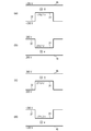
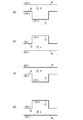
- FIG. 4 Schematic configuration diagram of a developing device and the like according to Embodiment 4 Schematic diagram of electric potential of conductor part 32, dielectric part 31, and regulating blade 4b according to the fourth embodiment. Schematic diagram of electric potential of conductor part 32, dielectric part 31, and regulating blade 4b according to the fifth embodiment. Schematic diagram of electric potential of conductor part 32, dielectric part 31, and regulating blade 4b according to the fifth embodiment. Schematic diagram of electric potential of conductor part 32, dielectric part 31, and regulating blade 4b according to Example 6
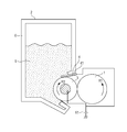
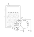
- the image forming apparatus 100 includes a photosensitive drum 1, a developing device 2, a cleaning device 8, a charging roller 7, an exposure device 91, a transfer roller 93, a fixing device 94, and the like as main components.
- the photosensitive drum 1, the developing device 2, the cleaning device 8, and the charging roller 7 are integrated as a process cartridge P, and the image forming apparatus main body (the portion of the image forming apparatus 100 excluding the process cartridge P) is integrated. It is configured to be detachable.
- the developing device 2 has a negative normal charging polarity (charging polarity for developing an electrostatic latent image. In this embodiment, since the negative electrostatic latent image is reversely developed, the normal charging polarity of the toner is negative). Contains toner with
- the exposure device 91 and the reflection mirror 92 are arranged so that the laser beam transmitted from the exposure device 91 reaches the exposure position A on the photosensitive drum 1 via the reflection mirror 92.
- a transfer roller 93 is disposed below the photosensitive drum 1.
- the transfer material S after the transfer is sent to the fixing device 94.
- a cleaning device 8 is installed downstream of the transfer position in the moving direction of the photosensitive drum.
- An attached blade is disposed so as to scrape off the toner on the photosensitive drum 1.
- the controller unit 70 comprehensively controls the following image forming operations according to a predetermined control program and reference table.
- the charging roller 7 charges the surface of the photosensitive drum 1 rotating at 100 mm / sec in the direction of the arrow R1 to a predetermined potential.
- an electrostatic latent image is formed on the photosensitive drum 1 by a laser beam transmitted from the exposure device 91 according to the image signal.
- the formed electrostatic latent image is developed by the developing device 2 at the development position C to form a toner image.
- the toner image formed on the photosensitive drum 1 is transferred to the transfer material S at the transfer position B.
- the transfer material S as a recording medium to which the toner image is transferred is sent to the fixing device 94.
- the fixing device 94 pressurizes and heats the toner image on the transfer material S to fix the toner image on the transfer material S to obtain a final image.
- FIG. 2 is a schematic configuration diagram of the developing device 2 and the like according to the present embodiment.
- the photosensitive drum 1 as an image carrier has an outer diameter of 24 mm and is driven to rotate in the direction of arrow R1 at a peripheral speed of 150 mm / sec.
- a developing device 2 is disposed on the left side of the photosensitive drum 1.
- the developing device 2 of the present embodiment includes a developing container 6, a developing roller 3, and a regulating blade 4, as shown in FIG.
- the developing container 6 stores toner 5 that is a non-magnetic one-component developer.
- the developing roller 3 as a toner carrier has an outer diameter of 12 mm and is driven to rotate in the direction of arrow R2 at a peripheral speed of 180 mm / sec.
- the developing roller 3 is disposed in contact with the surface of the photosensitive drum 1.
- the regulating blade 4 functions as a regulating unit that regulates the toner layer thickness on the developing roller.
- the regulation blade 4 includes a charging layer 41, a charge applying unit that applies a predetermined charge to the dielectric portion on the developing roller 3 via the toner 5, and a toner charging unit that applies a predetermined charge to the toner 5. As a function.
- the present invention has a configuration in which the toner supply member in contact with the developing roller 3 is omitted, and the above-described gradient force is used to carry a multilayer toner on the surface of the developing roller 3. Therefore, a dielectric portion and a conductor portion are provided on the surface of the developing roller 3, and the regulating blade 4 is rubbed through the toner to charge the dielectric portion, and a minute closed electric field is formed on a portion adjacent to the conductor portion. Form.
- the toner conveyed to the surface of the developing roller 3 receives a gradient force due to a minute closed electric field, and is sucked and carried on the surface of the developer carrying member.
- the surface of the developing roller 3 is configured such that a dielectric portion capable of holding electric charge and a conductor portion adjacent to the dielectric portion are exposed in a minute area.
- the developing roller 3 is configured to have an elastic layer 30b made of a conductive rubber material and a surface layer 30c on the outer periphery of the shaft core 30a.
- the developing roller 3 can be manufactured by forming a surface layer 30c made of a conductive resin material in which dielectric particles are dispersed on the elastic layer 30b by, for example, coating and polishing the surface.
- 3B is a plan view of the developing roller 3
- FIG. 3C is a cross-sectional view thereof.
- the size of the dielectric part 31 is preferably about 5 to 500 ⁇ m in outer diameter. This is an optimum value for holding charges on the surface and suppressing image unevenness.
- the outer diameter is greater than 5 ⁇ m, a sufficient charge can be retained on the surface of the dielectric portion 31 and a sufficiently small closed electric field can be formed.
- the outer diameter is smaller than 500 ⁇ m, the potential difference between the dielectric portion 31 and the conductor portion 32 does not become too large, and image unevenness can be suppressed.
- the dielectric portion 31 passes through the toner layer thickness regulation position by the regulation blade 4 and then passes through the toner layer thickness regulation position (during the rotation period T of the developing roller 3). Therefore, it is necessary to maintain a small electric field difference to some extent.
- the electric resistance value R and the electrostatic capacity C of the dielectric portion 31 satisfy CR ⁇ T / Ln10 (Ln: natural logarithm) with respect to the rotation period T of the developing roller 3.
- the dielectric part 31 charged at the toner layer thickness regulating position by the regulating blade 4 can maintain a charge amount of at least 10% after the rotation period T elapses.
- CR ⁇ 0.091 satisfies the above relationship and maintains a minute closed electric field.
- the electric resistance value R and the electrostatic capacitance C of the conductor portion 32 satisfy CR ⁇ T / Ln100 (Ln: natural logarithm) with respect to the rotation period T of the developing roller 3, for example.
- CR ⁇ 0.045 is satisfied so that the above relationship is satisfied and a minute closed electric field is formed.
- the volume resistivity of the dielectric particles was measured in a 23 ° C./50% RH environment by using a resistance measuring device “Hiresta-UP” manufactured by Mitsubishi Chemical Corporation and applying a voltage of 1000 V to the measurement target sample for 30 seconds. .
- the amount of the sample to be measured is preferably adjusted appropriately in consideration of the density of the particles to be measured. For example, when measuring acrylic resin particles, 0.6 g is used, and 2000 kgf / A sample to be measured was compressed by applying a pressure of cm 2 .
- the relative dielectric constant of the dielectric particles is measured as follows. First, a powder sample is put in a cylinder with a bottom area of 2.26 cm 2 and 15 kg of pressure is applied to the upper and lower electrodes.
- the CR measurement of the dielectric portion 31 on the surface of the developing roller 3 can be substituted by charging the dielectric portion 31 by a predetermined method and measuring the attenuation rate. For example, a measurement sample having a surface of 1 cm ⁇ 1 cm and a thickness of 3 mm is cut out from the developing roller 3, and + ions are emitted by a zero stat 3 manufactured by MILTY. Then, the potential of the dielectric portion 31 can be measured at a predetermined time interval in the KFM mode of a scanning probe microscope (SPA300, manufactured by SII Nanotechnology Co., Ltd.), and CR can be calculated from the potential decay rate.
- SPA300 scanning probe microscope
- acrylic resin particles are dispersed in a urethane resin as a binder.
- a conductive material used for imparting conductivity to the surface layer 30c carbon black or an ion conductive material can be used in the same manner.
- the urethane resin part functions as the conductor part 32 by setting the content of the conductive material of the surface layer 30c to 0.20 part by mass with respect to 100 parts by mass of the urethane resin.
- the dielectric part 31 is made of acrylic resin particles having an average particle diameter of 30 ⁇ m.
- the average particle diameter is 20 ° C., 0.01 mass% solid content concentration, 50% cumulative particle diameter value (d50) and 90% cumulative particle diameter value measured by DLS, particularly the microtrack method
- the content ratio of the acrylic resin particles is 70 parts by mass with respect to 100 parts by mass of the urethane resin, thereby obtaining the area ratio of the dielectric part / conductor part. In this case, the area of the dielectric portion is about 50% of the whole.
- the developing system in this embodiment uses the relationship between the dielectric portion 31 on the surface of the developing roller 3, the charging layer 41 of the regulating blade 4, and the work function of the toner.
- the work function of the material used for the dielectric portion on the surface of the developing roller 3 was 5.7 eV when measured using a surface analyzer (AC-2 type, manufactured by Riken Keiki Co., Ltd.) with an irradiation light amount of 250 nW.
- the regulating blade 4 in the present example was provided with a charging layer 41a.
- the above polyamide resin is laminated on a phosphor bronze metal sheet.
- the thickness of the phosphor bronze metal sheet was 0.1 mm
- the thickness of the polyamide resin was 0.1 mm.
- the work function of the charging layer 41 was 5.42 eV by the above-described measuring method.
- toner 5 in this example a negatively charged toner using a nonmagnetic styrene acrylic type + polyester type resin was used.
- the work function of Toner 5 was 6.01 eV by the measurement method described above.
- a DC voltage of ⁇ 300 V is applied from the DC power supply 61 to the developing roller 3 as a developing bias for contact development, and the photosensitive drum 1 is set to ⁇ 500 V for the solid white image portion and ⁇ 100 V for the solid image portion.
- the latent image was designed so that In this embodiment, in order to obtain a suitable image density, the toner coat amount on the photosensitive drum 1 at the time of solid image formation requires 0.54 mg / cm 2, so that the toner coat amount on the developing roller 3 is 0.45 mg / cm 2. Cost.
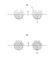
- FIG. 4 solid image formation
- FIG. 5 solid white image formation
- all the toner on the developing roller 3 is used for development for solid image formation.
- the white toner of the toner 5 shown in FIGS. 4 and 5 is an uncharged or low-charged toner
- the minus ( ⁇ )-labeled toner is a charged toner regulated by the surface of the developing roller 3 and the charged layer 41.
- a toner coat amount of about two layers can be obtained. That is, when the solid image is formed and the solid white image is formed, the amount of toner coating after passing through the restriction position is made equal, so that the occurrence of the ghost image described above can be suppressed. (Details will be described later)
- the white toner of the toner 5 shown in FIGS. 6 and 7 is an uncharged or low-charged toner, and the toner indicated by ⁇ (minus) is charged by the surface of the developing roller 3 and the charged layer 41, and the developing roller 3. This is a toner whose surface is rolled and charged.
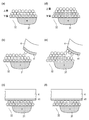
- FIGS. 6A, 6B, and 6C a mechanism in which toner adheres to the surface of the developing roller 3 during solid image formation, and a solid white image formation in FIGS. 6D, 6E, and 6F.
- the toner adhesion mechanism will be described.
- the surface of the developing roller 3 returns to the developing container 6 without the toner coat as shown in FIG.
- the uncharged or low-charged toner is attracted to the surface of the dielectric portion 31 where the minute closed electric field E is generated by a gradient force, and the toner that contacts the surface of the developing roller 3 is ⁇ Is charged.
- the adhered toner forms irregularities on the roller surface as shown in FIG.
- FIGS. 7A, 7B, and 7C a mechanism for regulating the toner layer on the surface of the developing roller 3 by the regulating blade 4 during solid image formation is shown in FIGS. 7D, 7E, and 7F.
- a mechanism for regulating the toner layer when forming a solid white image will be described.
- a toner layer of about four layers is formed on the surface of the developing roller 3 to be regulated.
- the minus toner on the surface of the developing roller 3 is easily peeled off from the surface of the developing roller 3 by the electric field between the charging layer 41 and the dielectric portion 31. At this time, the amount of toner that is peeled off by the electric field is larger because minus toner is laminated on the upper layer as compared with the case of solid image formation.
- the toner coating amount after passing through the regulation position at the time of solid image formation is made equal by the toner adhesion mechanism on the surface of the developing roller 3 and the toner layer regulation mechanism described above.
- ghost image generation can be greatly improved.
- the details of the comparison between the solid image formation and the solid white image formation in which the difference in the toner coat state on the surface of the developing roller 3 is most likely to appear are described.
- the subsequent toner coat amount can be made equal.
- the A4 size of 1000 sheets was formed by the image forming apparatus of FIG. 1 of the present embodiment, a favorable image was obtained while maintaining a suitable image density and without causing image defects.
- the image forming apparatus includes the developing roller 3 in which the dielectric portions 31 are scattered on the surface, and the dielectric portion 31 has the same regular charging polarity of toner as the regulation blade 4 in the charging series.
- Each member is configured to be positioned on the polar side. Accordingly, it is possible to provide an image forming apparatus that suppresses a decrease in density at the rear end of the solid image and suppresses the occurrence of ghosts using the developing device that does not include the developer supply member.
- the developing roller 3, the regulating blade 4, and the toner 5 have the above-described material configurations, but the dielectric portion is positioned on the same polarity side as the regular charging polarity of the toner with respect to the regulating blade 4 in the charging series. What is necessary is just to do and is not restricted to the above-mentioned material amount composition.
- each material is composed of ( ⁇ ) charged layer 41 ⁇ dielectric portion 31 ⁇ toner 5 (+), and the potentials of the conductor portion 32, the dielectric portion 31, and the charged layer 41 are configured. The relationship can be as shown in FIG.
- the conductivity of the charging layer 41 can obtain the effect of the present invention in both cases of conduction and insulation, but it prevents the charge on the elastic blade from being charged up and prevents the toner from having an unnecessary charge. Is preferably conductive.
- the tip surface of the regulating blade 4 is arranged so as to face the normal direction with respect to the developing roller 3 so that the effect of the present invention can be further extracted. That is, the guide blade 4 p that guides the toner to the outside of the facing area X between the control blade 4 and the developing roller 3 is provided at the tip of the control blade 4. The guide portion 4p is positioned on the side opposite to the normal charging polarity of the toner from the dielectric portion 31 on the charging series. As a result, as shown in FIG.
- the upper layer minus toner peeled off by the electric field adheres to the charging layer 41 of the guide portion 4p, and is pushed up by the minus toner conveyed one after another to the direction of the arrow. To be guided to. For this reason, the minus toner peeled off by the electric field does not stay in the vicinity of the regulation position, and the upper layer minus toner on the surface of the developing roller 3 is more reliably peeled off. Therefore, the ghost improvement effect of the present invention can be further enhanced.
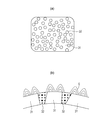
- the developing roller 3 in this embodiment uses a configuration in which the dielectric portions 31 are scattered on the surface.
- “scattering” is not limited to the state where the dielectric portions are separated from each other, but is used to include the state where the dielectric portions are continuous as shown in FIG. 10A, for example. . That is, the dielectric part 31 should just be distributed regularly or irregularly in a certain ratio with respect to the whole surface, without solidifying in one place.
- the dielectric portion 31 corresponds to the sea in the sea-island type
- the conductor portion 32 corresponds to the island in the sea-island type.
- the conductor portion 32 is in contact with the lower conductive layer.
- a minute closed electric field is formed as shown by the electric lines of force E in FIG. The same effect as can be achieved.
- the photosensitive drum 1 and the developing roller 3 are arranged in contact with each other.
- the photosensitive drum 1 and the developing roller 3a are arranged in a non-contact manner as shown in FIG. May be.
- the knurled developing roller 3a shown in FIG. 12 it is easy to control the size and area ratio of the dielectric portion / conductor portion.
- an insulating resin for example, is coated. Then, the surface can be cut to expose the cored bar portion as the conductor portion 32 and the resin in the groove as the dielectric portion 31, respectively.
- FIG. 12A is a plan view of the developing roller 3a, and FIG.
- the aforementioned acrylic resin is used for the dielectric particles.
- an elastic blade 4a provided with a charging layer 41a is used as the regulating member.
- development is performed by applying a bias in which an AC bias and a DC bias are superimposed as a development bias from the power source 62.
- the image forming apparatus described in the first embodiment has a configuration in which a convex portion is provided on the surface of the developing roller 3 and a dielectric portion 31 is present on the convex portion, as shown in FIG. .
- the tip surface of the regulating blade 4 is arranged so as to face the normal direction with respect to the developing roller 3 so that the unevenness on the surface of the developing roller 3 can be easily followed.
- Other main configurations are the same as those in the first embodiment.
- the dielectric portion 31 by providing the dielectric portion 31 on the convex portion, the dielectric portion 31 can be directly triboelectrically charged to the charging layer 41, and the dielectric portion 31 is charged to-of the same polarity as the toner. Can do.
- the developing roller 3 in this embodiment is configured to have an elastic layer 30b made of a conductive rubber material and a surface layer 30c on the outer periphery of the shaft core 30a.
- FIG. 13B is a plan view of the developing roller 3
- FIG. 13C is a cross-sectional view.
- the surface layer 30c is a sea-island type phase composed of a domain phase containing a polyester copolymer resin consisting of chemical formulas (A) and (B) and a matrix phase of a polyester melamine resin containing chemical formulas (A), (B) and (C). It has a separation structure.
- R 1 is a linear alkylene group having 2 to 9 carbon atoms or a branched alkylene group having 6 to 9 carbon atoms
- R 2 is a linear alkylene group having 2 to 8 carbon atoms. It is a group.
- the surface layer is characterized in that a domain phase composed of a dielectric portion and a matrix phase composed of a conductor portion in which conductive fine particles are unevenly distributed are exposed in a minute area, and the domain phase functions as the dielectric portion 31b.
- the matrix phase functions as the conductor portion 32b.
- the equivalent circle diameter of the dielectric portion 31b is preferably 10 ⁇ m or more. By setting the thickness to 10 ⁇ m or more, it is possible to obtain a charging potential amount sufficient to hold the toner.
- the equivalent circle diameter refers to the diameter of a circle having the same area as the area of the domain phase projected onto the surface of the developing roller.
- the domain phase in the present invention can be identified by a scanning electron microscope (SEM), a scanning transmission electron microscope (STEM), or the like. The area ratio of both parts is such that the area of the dielectric part is about 50% of the whole.
- the thickness of the surface layer 30c is 10 ⁇ m. Further, the surface roughness of the developing roller 3 having a convex dielectric portion can be controlled by controlling the phase separation structure.
- a method of forming a coating film having a sea-island type phase separation structure there is a method of forming a coating film by dissolving a resin material having high crystallinity and a solid state in a supersaturated amount of solvent at room temperature.
- a resin material with high crystallinity exhibits the property that crystals are likely to precipitate partially due to volatilization of the solvent during coating film formation.
- the crystal-like precipitation portion becomes the domain portion, and the portion where the coating film is continuously formed becomes the matrix portion, thereby forming a sea-island type phase separation structure.
- This domain phase that is, crystal precipitation, depends on the crystallinity of the polyester copolymer resin in this embodiment.
- control of the crystal size and the coverage is important to control the crystal size and the coverage by optimizing the molecular structure of the crystallinity of the polyester copolymer resin.
- control of the phase separation structure that is, the size of the domain, can be achieved by the boiling point, evaporation rate, and SP value of the solvent.
- the uneven distribution of the conductive fine particles in the matrix phase was confirmed by performing mapping analysis with a scanning probe microscope (SPM).
- SPM scanning probe microscope
- the domain-like region showed insulation, while the surrounding matrix region was confirmed to be conductive.
- the work function of the material used for the dielectric portion on the surface of the developing roller 3 was 5.6 eV when measured using a surface analyzer (AC-2 type, manufactured by Riken Keiki Co., Ltd.) with an irradiation light amount of 250 nW. It was.
- the dielectric portion 31b when the toner particle size is smaller than the height of the convex portion of the dielectric portion 31b, the dielectric portion 31b is negatively charged by friction with the charging layer 41. To do. As shown in FIG. 14B, when the toner particle diameter is larger than the height of the convex portion of the dielectric portion 31b, the dielectric portion 31b does not rub against the charging layer 41, but is positively charged by friction with the toner. .
- the ghost image improvement mechanism in this embodiment will be described.
- the difference from the first embodiment is that the dielectric portion 31 is present on the convex portion, and can have both positive and negative polarities depending on the relationship between the height of the convex portion and the toner particle size.
- the toner suction to the surface of the developing roller 3 in the present invention is a gradient force due to a minute closed electric field, so the direction of the force received by the toner does not depend on the direction of the electric field, and Receive force in the direction of increasing.
- the case where the dielectric 31 is negative will be described in detail in Example 3. Therefore, the mechanism for improving the ghost image is the same as that in the first embodiment, and a detailed description thereof is omitted.
- FIGS. 15A, 15B, and 15C are explanatory views showing that toner adheres to the surface of the developing roller 3 when a solid image is formed.
- FIGS. 15D, 15E, and 15F when a solid white image is formed.
- the toner adhesion explanatory drawing is shown.
- 16A, 16B, and 16C are explanatory diagrams for regulating the toner layer on the surface of the developing roller 3 during solid image formation by the regulating blade 4, and in FIGS. 16D, 16E, and 16F, FIG. 6 is an explanatory diagram of toner layer regulation during solid white image formation.
- Table 1 shows the relationship between the average toner particle diameter r, the developing roller 3 surface roughness Rzjis (ten-point average roughness), and ghost / fogging when an image of A4 size 10000 sheets is formed using the developing device of this embodiment. Shown in
- the occurrence of ghost when the surface Rzjis of the developing roller 3 is small is because a minute closed electric field cannot be formed due to friction between the dielectric portion 31b and the toner due to toner fusion to the dielectric portion 31.
- the surface Rzjis of the developing roller 3 is increased, the dielectric portion 31b is charged with the same polarity as the toner due to friction with the charging layer 41, so that the occurrence of toner fusion can be suppressed.
- Rzjis increases, the proportion of the dielectric portion 31b charged to the same polarity as the toner increases, and by setting Rzjis ⁇ r (toner average particle diameter), toner fusion can be significantly suppressed.
- the ratio of the dielectric portion 31b charged to the same polarity as the toner is determined by Rzjis and the particle size distribution of the toner.
- the reason why fog occurs when Rzjis> 3r is that three toner layers are easily formed on the unevenness of the surface of the developing roller 3, and the toner and the layer sandwiched between the toners cannot be charged. Therefore, in order to suppress fogging, it is desirable to satisfy Rzjis ⁇ 3r.
- the image forming apparatus includes the developing roller 3 in which the dielectric portions 31 are scattered on the surface, and the dielectric portion 31 has the same regular charging polarity of toner as the regulation blade 4 in the charging series.
- Each member is configured to be positioned on the polar side. Accordingly, it is possible to provide an image forming apparatus capable of realizing a long life by suppressing a decrease in density at the rear end of a solid image and suppressing generation of a ghost by using a developing device without a developer supply member. it can.
- the above-described method is adopted for forming the surface roughness of the developing roller 3, but the effect of the present invention can be achieved if the dielectric portion 31b is convex and a predetermined surface roughness can be obtained. It is not limited to.
- the present embodiment can be applied to a configuration in which a surface layer of a conductive resin in which insulating particles are dispersed is coated on a conductive substrate and the insulating particles are projected by polishing the surface to obtain a predetermined surface roughness. The same effect as can be achieved.
- FIG. 17 a developer in which an external additive 51 is dispersed on the surface of the toner 5 is employed in the image forming apparatus described in the first embodiment.
- an external additive 51 positioned on the opposite side of the normal charging polarity of the toner 5 from the dielectric portion 31 in the charging series is externally added to the surface of the toner 5, and the dielectric portion 31 is externally attached.
- the additive 51 is charged to the same polarity as the normal charging polarity of the toner.
- the dielectric part 31 is normally charged with toner. It is characterized by being charged to the same polarity as-.
- Other main configurations are the same as those in the first embodiment.
- titanium oxide was used as an external additive, and 0.5 parts by mass of the external additive was stirred at a high speed with respect to 100 parts by mass of the toner to prepare a developer by treating the toner surface.
- the development system in this embodiment uses the relationship between the work functions of the dielectric portion 31 on the surface of the developing roller 3, the toner 5, and the external additive 51.
- the work functions of the toner 5 and the external additive 51 were 6.01 eV and 5.41 eV according to the measurement method described above.
- the material of the toner 5 and the external additive 51 are selected so as to have the above-described work function, so that ( ⁇ ) toner 5 ⁇ dielectric portion 31 ⁇ charged layer 41 ⁇ external additive 51 in the charge series. (+).
- the work function difference between the toner 5 and the dielectric part 31 is smaller than the difference between the dielectric part 31 and the external additive 51, and the work function difference between the toner 5 and the charge layer 41 is changed between the charged layer 41 and the external additive 51. It is configured to be larger than the difference.
- the toner 5 is negatively charged and the external additive 51 is positively charged due to friction between the toner 5 and the dielectric part 31, and the dielectric part 31 has an external work function with a larger work function difference. It is negatively charged by friction with the additive 51.
- the charging layer 41 is positively charged due to the friction with the toner 5 having a larger work function difference.
- the ghost image improvement mechanism in this embodiment will be described.
- the difference from the first embodiment is that the dielectric portion 31 has a negative polarity. Since the toner suction to the surface of the developing roller 3 in the present invention is a gradient force due to a minute closed electric field, the direction of the force applied to the toner is not dependent on the direction of the electric field but receives the force in the direction of increasing the electric field. Therefore, as shown in FIGS. 18A and 18B, even if the dielectric portion 31 has the same polarity as that of the toner, the toner can be attracted if a minute closed electric field is formed.
- the mechanism by which toner adheres to the surface of the developing roller 3 during solid image formation and solid white image formation is the same as in the first embodiment.
- Vdc developing bias
- the dielectric portion 31 Vdc ⁇
- Layer 41 Vdc + ⁇ .
- the ghost image generation mechanism described above can suppress the generation of ghost images by equalizing the toner coat amount after passing through the regulation position during solid image formation and solid white image formation. it can.
- Table 2 shows the results of image formation on the A4 size 10,000 sheets using the image forming apparatus of FIG. 1 for the developing device of Example 1 and the developing device of this example.
- Example 3 since the dielectric part 31 has the same polarity as the toner, the occurrence of toner fusion can be reduced and a long life can be realized.
- the image forming apparatus includes the developing roller 3 in which the dielectric portions 31 are scattered on the surface, and the dielectric portion 31 has the same regular charging polarity of toner as the regulation blade 4 in the charging series.
- Each member is configured to be positioned on the polar side. Accordingly, it is possible to provide an image forming apparatus that suppresses a decrease in density at the rear end of the solid image and suppresses the occurrence of ghosts using the developing device that does not include the developer supply member.
- the toner 5, the dielectric portion 31, and the charging layer 41 have the above-described material configurations, but are not limited thereto.
- each material is composed of ( ⁇ ) external additive 51 ⁇ charged layer 41 ⁇ dielectric portion 31 ⁇ toner 5 (+), and the conductor portion 32, dielectric portion 31,
- the potential relationship of the charging layer 41 can be as shown in FIG.
- ( ⁇ ) toner 5 ⁇ dielectric portion 31 ⁇ charge layer 41 ⁇ external additive 51 (+) in the charging series is used, but ( ⁇ ) toner 5 ⁇ dielectric portion 31 ⁇ outside.
- the additive 51 ⁇ charged layer 41 (+) may be satisfied.
- the dielectric part 31 can be charged to a negative polarity having the same polarity as the toner. The same effects as in the present embodiment can be obtained.
- titanium oxide is used as the external additive 51, but it is not particularly limited as long as it satisfies the above-mentioned position on the charging series in the following known inorganic powder. Specifically, oxides of metals such as magnesium, zinc and aluminum, composite metal oxides such as calcium titanate, metal salts such as calcium carbonate, etc. satisfying the above position on the charging series Can be used.
- an electric field that causes the toner to be peeled off from the dielectric portion 31 is formed by a blade bias.
- the developing roller 3 is connected to a DC power source 71 for applying a developing bias Vdc.
- Other main configurations are the same as those in the first embodiment.
- Vmf The potential difference (hereinafter referred to as Vmf) between the dielectric part 31 and the conductor part 32 during image formation was measured according to the following procedure.
- SPA300 scanning probe microscope
- the value measured in (2) above is 20V.
- Table 3 shows the results when an image was formed by applying a blade bias in this example.
- the potential difference (Vbr ⁇ Vdc) between the blade bias Vbr and the developing bias Vdc is set to be positive.
- an electric field is generated in the direction in which the toner moves from the surface of the developing roller 3 to the regulating blade 4b.
- the ghost image is improved by changing the potential difference (Vbr ⁇ Vdc) from minus to plus.
- the mechanism for improving the ghost image is the same as in the first embodiment, and is because the upper layer toner in FIGS. 7B and 7E is peeled off by the electric field generated by the potential difference (Vbr ⁇ Vdc).
- Vmf 21.3V
- the ghost image is significantly improved by setting the potential difference (Vbr ⁇ Vdc) to + 25V to + 50V, which is larger than Vmf.
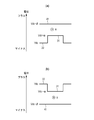
- FIG. 21A is a schematic diagram of the potential of the conductor portion 32, the dielectric portion 31, and the regulating blade 4, which are modified examples of the present embodiment, and FIGS. Show.
- FIG. 21A shows a case where the toner is negative and the developing bias is negative.
- FIG. 21B shows the case where the toner is positive and the developing bias is positive.
- FIG. 21C shows the case where the toner is negative and the developing bias is positive.
- FIG. 21D shows a case where the toner has positive polarity and the developing bias is negative.
- the potential relationship is set such that an electric field for removing the toner from the dielectric portion 31 is generated.
- the electric potential of the conductor portion 32, the dielectric portion 31, and the regulating blade 4 were set as shown in FIG. A suitable image density was maintained, and a good image was obtained without image defects.
- the image forming apparatus includes the developing roller 3 in which the dielectric portions 31 are scattered on the surface, and the potential difference obtained by subtracting the potential of the dielectric portion 31 from the potential of the regulating blade 4b is opposite to the normal charging polarity of the toner.
- a voltage is applied to the regulating blade 4b so as to be polar. Accordingly, it is possible to provide an image forming apparatus that suppresses a decrease in density at the rear end of the solid image and suppresses the occurrence of ghosts using the developing device that does not include the developer supply member.
- Table 4 shows the results when an image was formed by applying a blade bias in this example.
- the potential difference (Vbr ⁇ Vdc) between the blade bias Vbr and the developing bias Vdc is set to be positive.
- an electric field is generated in the direction in which the toner moves from the surface of the developing roller 3 to the regulating blade 4b.
- Vmf 21.3V as in the fourth embodiment.
- the ghost image is improved by changing the potential difference (Vbr ⁇ Vdc) from minus to plus.
- the mechanism for improving the ghost image is the same as in the third embodiment, and is because the upper layer toner in FIGS. 19B and 19E is peeled off by the electric field generated by the potential difference (Vbr ⁇ Vdc).
- the dielectric part 31 is negatively charged by friction with the charging layer 41. Otherwise, the dielectric part 31 is Charges positively due to friction with toner.
- the dielectric portion 31b has a high ratio of being charged to-, but there is also a dielectric portion 31 that is charged to +.
- the potential schematic diagram in the present embodiment employs FIGS. 22A, 22B, 22C, and 22D when the dielectric portion 31b includes both the one that is charged to the same polarity as the toner and the other that are not.
- FIGS. 23A, 23B, 23C, and 23D are employed.
- the mechanism for suppressing the toner fusion to the dielectric portion 31 due to the increase in the number of formed images is the same as in the third embodiment.
- the electric potential of the conductor portion 32, the dielectric portion 31, and the regulating blade 4 were set as shown in FIG. 22A, and image formation of 10,000 sheets of A4 size was performed. A suitable image density was maintained, and a good image was obtained without image defects.
- the image forming apparatus includes the developing roller 3 in which the dielectric portions 31 are scattered on the surface, and the potential difference obtained by subtracting the potential of the dielectric portion 31 from the potential of the regulating blade 4b is opposite to the normal charging polarity of the toner.
- a voltage is applied to the regulating blade 4b so as to be polar. Accordingly, it is possible to provide an image forming apparatus capable of realizing a long life by suppressing a decrease in density at the rear end of a solid image and suppressing generation of a ghost by using a developing device without a developer supply member. it can.
- Table 5 shows the results when an image was formed by applying a blade bias in this example.
- the potential difference (Vbr ⁇ Vdc) is set so that the potential difference (Vbr ⁇ Vdc) between the blade bias Vbr and the developing bias Vdc is positive.
- Vbr ⁇ Vdc potential difference between the blade bias Vbr and the developing bias Vdc
- the ghost image is improved by changing the potential difference (Vbr ⁇ Vdc) from minus to plus.
- the mechanism for improving the ghost image is the same as in the second embodiment, and is because the upper layer toner in FIGS. 7B and 7E is peeled off by the electric field due to the potential difference (Vbr ⁇ Vdc).
- the conductor portion 32 since the dielectric portion 31 is charged with the same polarity ( ⁇ ) as that of the toner, the conductor portion 32 has a potential that is more difficult to peel off by an electric field. Therefore, by setting the potential difference (Vbr ⁇ Vdc)> 0, an electric field that peels off the toner from both the dielectric portion 31 and the conductor portion 32 can be formed, and the ghost image is greatly improved.
- FIG. 24A shows a potential schematic diagram of the conductor portion 32, the dielectric portion 31, and the regulating blade 4b, which are modified examples of this embodiment, and FIGS. Show. 24A shows the case where the toner has a negative polarity and the development bias is negative, FIG. 24B shows the case where the toner has a positive polarity and the development bias has a positive polarity, and FIG. 24C shows the case where the toner has a negative polarity. When the bias is positive, FIG. 24D shows the case where the toner is positive and negative and the developing bias is negative. In any case, the potential relationship is set such that an electric field for removing the toner from the dielectric portion 31 is generated.
- the mechanism for suppressing the toner fusion to the dielectric portion 31 due to the increase in the number of image formations is the same as in the second embodiment.
- the conductor part 32, the dielectric part 31, and the regulating blade 4 potential are set as shown in FIG. A good image was obtained while maintaining a high image density and without image defects.
- the image forming apparatus includes the developing roller 3 in which the dielectric portions 31 are scattered on the surface, and the potential difference obtained by subtracting the potential of the dielectric portion 31 from the potential of the regulating blade 4b is opposite to the normal charging polarity of the toner.
- a voltage is applied to the regulating blade 4b so as to be polar. Accordingly, it is possible to provide an image forming apparatus capable of realizing a long life by suppressing a decrease in density at the rear end of a solid image and suppressing generation of a ghost by using a developing device without a developer supply member. it can.
Landscapes
- Physics & Mathematics (AREA)
- General Physics & Mathematics (AREA)
- Dry Development In Electrophotography (AREA)
- Developing Agents For Electrophotography (AREA)
Priority Applications (3)
| Application Number | Priority Date | Filing Date | Title |
|---|---|---|---|
| JP2014501859A JP5989081B2 (ja) | 2012-02-27 | 2012-02-27 | 現像装置、プロセスカートリッジおよび画像形成装置 |
| PCT/JP2012/054799 WO2013128551A1 (fr) | 2012-02-27 | 2012-02-27 | Dispositif de développement, cartouche de traitement et dispositif de formation d'image |
| US13/776,333 US9098010B2 (en) | 2012-02-27 | 2013-02-25 | Development device, process cartridge, and image forming apparatus |
Applications Claiming Priority (1)
| Application Number | Priority Date | Filing Date | Title |
|---|---|---|---|
| PCT/JP2012/054799 WO2013128551A1 (fr) | 2012-02-27 | 2012-02-27 | Dispositif de développement, cartouche de traitement et dispositif de formation d'image |
Publications (1)
| Publication Number | Publication Date |
|---|---|
| WO2013128551A1 true WO2013128551A1 (fr) | 2013-09-06 |
Family
ID=49003015
Family Applications (1)
| Application Number | Title | Priority Date | Filing Date |
|---|---|---|---|
| PCT/JP2012/054799 Ceased WO2013128551A1 (fr) | 2012-02-27 | 2012-02-27 | Dispositif de développement, cartouche de traitement et dispositif de formation d'image |
Country Status (3)
| Country | Link |
|---|---|
| US (1) | US9098010B2 (fr) |
| JP (1) | JP5989081B2 (fr) |
| WO (1) | WO2013128551A1 (fr) |
Cited By (17)
| Publication number | Priority date | Publication date | Assignee | Title |
|---|---|---|---|---|
| JP2013174808A (ja) * | 2012-02-27 | 2013-09-05 | Canon Inc | 導電性部材、プロセスカートリッジおよび電子写真画像形成装置 |
| US9098014B2 (en) | 2013-08-23 | 2015-08-04 | Canon Kabushiki Kaisha | Developing device and image forming apparatus |
| US9213258B2 (en) | 2013-08-23 | 2015-12-15 | Canon Kabushiki Kaisha | Developing assembly, process cartridge, and image-forming apparatus |
| US9250564B2 (en) | 2013-08-23 | 2016-02-02 | Canon Kabushiki Kaisha | Developing device and image forming apparatus |
| US9256156B2 (en) | 2013-08-23 | 2016-02-09 | Canon Kabushiki Kaisha | Developing assembly, process cartridge, and image-forming apparatus |
| JP2016051097A (ja) * | 2014-09-01 | 2016-04-11 | キヤノン株式会社 | 画像形成装置 |
| JP2016164654A (ja) * | 2015-02-27 | 2016-09-08 | キヤノン株式会社 | 電子写真用部材、プロセスカートリッジおよび電子写真画像形成装置 |
| JP2017090824A (ja) * | 2015-11-16 | 2017-05-25 | キヤノン株式会社 | 現像部材、現像部材の製造方法、プロセスカートリッジおよび電子写真装置 |
| JP2017156745A (ja) * | 2016-02-26 | 2017-09-07 | キヤノン株式会社 | 現像ローラ、プロセスカートリッジおよび電子写真画像形成装置 |
| JP2017215458A (ja) * | 2016-05-31 | 2017-12-07 | キヤノン株式会社 | 現像部材、電子写真プロセスカートリッジ及び電子写真画像形成装置 |
| JP2018025767A (ja) * | 2016-07-29 | 2018-02-15 | キヤノン株式会社 | 現像装置、電子写真プロセスカートリッジ及び電子写真画像形成装置 |
| JP2020027173A (ja) * | 2018-08-10 | 2020-02-20 | キヤノン株式会社 | 画像形成装置 |
| JP2020027172A (ja) * | 2018-08-10 | 2020-02-20 | キヤノン株式会社 | プロセスカートリッジおよび画像形成装置 |
| JP2020038366A (ja) * | 2018-08-30 | 2020-03-12 | キヤノン株式会社 | 現像ローラ、プロセスカートリッジおよび電子写真画像形成装置 |
| JP2020067577A (ja) * | 2018-10-25 | 2020-04-30 | キヤノン株式会社 | 現像装置、現像剤担持体、プロセスカートリッジおよび画像形成装置 |
| JP2020067578A (ja) * | 2018-10-25 | 2020-04-30 | キヤノン株式会社 | 現像剤担持体、現像装置、プロセスカートリッジおよび画像形成装置 |
| US10747140B2 (en) | 2018-10-25 | 2020-08-18 | Canon Kabushiki Kaisha | Developing apparatus, developer carrying member, process cartridge, and image forming apparatus |
Families Citing this family (4)
| Publication number | Priority date | Publication date | Assignee | Title |
|---|---|---|---|---|
| JP5952796B2 (ja) * | 2013-10-16 | 2016-07-13 | 京セラドキュメントソリューションズ株式会社 | 画像形成装置、及び画像形成方法 |
| JP6271958B2 (ja) * | 2013-11-13 | 2018-01-31 | キヤノン株式会社 | 画像形成装置 |
| US11845127B2 (en) * | 2018-06-08 | 2023-12-19 | Hewlett-Packard Development Company, L.P. | Powder layer former with flowing gas seal |
| JP2025088860A (ja) * | 2023-12-01 | 2025-06-12 | キヤノン株式会社 | プロセスカートリッジ及びプロセスカートリッジセット |
Citations (4)
| Publication number | Priority date | Publication date | Assignee | Title |
|---|---|---|---|---|
| JPH03233477A (ja) * | 1989-12-07 | 1991-10-17 | Fujitsu Ltd | 現像装置 |
| JPH0713410A (ja) * | 1993-06-19 | 1995-01-17 | Ricoh Co Ltd | 現像装置 |
| JP3162219B2 (ja) * | 1992-10-16 | 2001-04-25 | 株式会社リコー | 現像装置 |
| JP3272056B2 (ja) * | 1992-10-15 | 2002-04-08 | 株式会社リコー | 現像装置 |
Family Cites Families (9)
| Publication number | Priority date | Publication date | Assignee | Title |
|---|---|---|---|---|
| US4200665A (en) * | 1974-06-18 | 1980-04-29 | Koichi Suzuki | Method for controlling the toner concentration of a developer used in a dry type developing system |
| JPH0812510B2 (ja) * | 1986-10-17 | 1996-02-07 | ミノルタ株式会社 | 静電潜像現像装置 |
| US5339141A (en) * | 1992-02-16 | 1994-08-16 | Ricoh Company, Ltd. | Developing device with a developer carrier capable of forming numerous microfields thereon |
| US5467175A (en) * | 1992-12-30 | 1995-11-14 | Ricoh Company, Ltd. | Developing device for an image forming apparatus |
| JP3285274B2 (ja) * | 1994-05-30 | 2002-05-27 | 株式会社リコー | 現像装置 |
| US5742885A (en) * | 1996-06-24 | 1998-04-21 | Xerox Corporation | Development system employing acoustic toner fluidization for donor roll |
| JPH10307472A (ja) * | 1997-05-08 | 1998-11-17 | Minolta Co Ltd | 現像装置 |
| JP4939616B2 (ja) * | 2010-01-29 | 2012-05-30 | 株式会社沖データ | 現像装置及び画像形成装置 |
| JP5869912B2 (ja) * | 2012-02-27 | 2016-02-24 | キヤノン株式会社 | 導電性部材、プロセスカートリッジおよび電子写真画像形成装置 |
-
2012
- 2012-02-27 WO PCT/JP2012/054799 patent/WO2013128551A1/fr not_active Ceased
- 2012-02-27 JP JP2014501859A patent/JP5989081B2/ja active Active
-
2013
- 2013-02-25 US US13/776,333 patent/US9098010B2/en active Active
Patent Citations (4)
| Publication number | Priority date | Publication date | Assignee | Title |
|---|---|---|---|---|
| JPH03233477A (ja) * | 1989-12-07 | 1991-10-17 | Fujitsu Ltd | 現像装置 |
| JP3272056B2 (ja) * | 1992-10-15 | 2002-04-08 | 株式会社リコー | 現像装置 |
| JP3162219B2 (ja) * | 1992-10-16 | 2001-04-25 | 株式会社リコー | 現像装置 |
| JPH0713410A (ja) * | 1993-06-19 | 1995-01-17 | Ricoh Co Ltd | 現像装置 |
Cited By (22)
| Publication number | Priority date | Publication date | Assignee | Title |
|---|---|---|---|---|
| JP2013174808A (ja) * | 2012-02-27 | 2013-09-05 | Canon Inc | 導電性部材、プロセスカートリッジおよび電子写真画像形成装置 |
| US9098014B2 (en) | 2013-08-23 | 2015-08-04 | Canon Kabushiki Kaisha | Developing device and image forming apparatus |
| US9213258B2 (en) | 2013-08-23 | 2015-12-15 | Canon Kabushiki Kaisha | Developing assembly, process cartridge, and image-forming apparatus |
| US9250564B2 (en) | 2013-08-23 | 2016-02-02 | Canon Kabushiki Kaisha | Developing device and image forming apparatus |
| US9256156B2 (en) | 2013-08-23 | 2016-02-09 | Canon Kabushiki Kaisha | Developing assembly, process cartridge, and image-forming apparatus |
| JP2016051097A (ja) * | 2014-09-01 | 2016-04-11 | キヤノン株式会社 | 画像形成装置 |
| JP2016164654A (ja) * | 2015-02-27 | 2016-09-08 | キヤノン株式会社 | 電子写真用部材、プロセスカートリッジおよび電子写真画像形成装置 |
| JP2017090824A (ja) * | 2015-11-16 | 2017-05-25 | キヤノン株式会社 | 現像部材、現像部材の製造方法、プロセスカートリッジおよび電子写真装置 |
| JP2017156745A (ja) * | 2016-02-26 | 2017-09-07 | キヤノン株式会社 | 現像ローラ、プロセスカートリッジおよび電子写真画像形成装置 |
| JP2017215458A (ja) * | 2016-05-31 | 2017-12-07 | キヤノン株式会社 | 現像部材、電子写真プロセスカートリッジ及び電子写真画像形成装置 |
| JP2018025767A (ja) * | 2016-07-29 | 2018-02-15 | キヤノン株式会社 | 現像装置、電子写真プロセスカートリッジ及び電子写真画像形成装置 |
| JP2020027173A (ja) * | 2018-08-10 | 2020-02-20 | キヤノン株式会社 | 画像形成装置 |
| JP2020027172A (ja) * | 2018-08-10 | 2020-02-20 | キヤノン株式会社 | プロセスカートリッジおよび画像形成装置 |
| JP7150517B2 (ja) | 2018-08-10 | 2022-10-11 | キヤノン株式会社 | プロセスカートリッジおよび画像形成装置 |
| JP7150518B2 (ja) | 2018-08-10 | 2022-10-11 | キヤノン株式会社 | 画像形成装置 |
| JP2020038366A (ja) * | 2018-08-30 | 2020-03-12 | キヤノン株式会社 | 現像ローラ、プロセスカートリッジおよび電子写真画像形成装置 |
| JP7433805B2 (ja) | 2018-08-30 | 2024-02-20 | キヤノン株式会社 | 現像ローラ、プロセスカートリッジおよび電子写真画像形成装置 |
| JP2020067577A (ja) * | 2018-10-25 | 2020-04-30 | キヤノン株式会社 | 現像装置、現像剤担持体、プロセスカートリッジおよび画像形成装置 |
| JP2020067578A (ja) * | 2018-10-25 | 2020-04-30 | キヤノン株式会社 | 現像剤担持体、現像装置、プロセスカートリッジおよび画像形成装置 |
| US10747140B2 (en) | 2018-10-25 | 2020-08-18 | Canon Kabushiki Kaisha | Developing apparatus, developer carrying member, process cartridge, and image forming apparatus |
| JP7195871B2 (ja) | 2018-10-25 | 2022-12-26 | キヤノン株式会社 | 現像装置、現像剤担持体、プロセスカートリッジおよび画像形成装置 |
| JP7207943B2 (ja) | 2018-10-25 | 2023-01-18 | キヤノン株式会社 | 現像剤担持体、現像装置、プロセスカートリッジおよび画像形成装置 |
Also Published As
| Publication number | Publication date |
|---|---|
| JP5989081B2 (ja) | 2016-09-07 |
| JPWO2013128551A1 (ja) | 2015-07-30 |
| US20130223891A1 (en) | 2013-08-29 |
| US9098010B2 (en) | 2015-08-04 |
Similar Documents
| Publication | Publication Date | Title |
|---|---|---|
| JP5989081B2 (ja) | 現像装置、プロセスカートリッジおよび画像形成装置 | |
| JP6157276B2 (ja) | 現像装置、プロセスカートリッジ、画像形成装置 | |
| JP2015041084A (ja) | 現像装置、プロセスカートリッジ、画像形成装置 | |
| JP3652331B2 (ja) | 画像形成装置 | |
| JP6242173B2 (ja) | 現像剤担持体、現像装置、プロセスカートリッジ、画像形成装置 | |
| JP2015094894A (ja) | 画像形成装置 | |
| JP2005173242A (ja) | 現像装置、カートリッジ及び画像形成装置 | |
| JP3332865B2 (ja) | 画像形成装置 | |
| KR101764963B1 (ko) | 현상제 담지체, 현상 조립체, 프로세스 카트리지 및 화상 형성 장치 | |
| US9250564B2 (en) | Developing device and image forming apparatus | |
| JP2015041083A (ja) | 現像装置、画像形成装置 | |
| JP2008051901A (ja) | クリーニングブレード及び画像形成装置 | |
| JP2007316618A (ja) | 画像形成装置およびそれに用いられるプロセスカートリッジ | |
| JP6478671B2 (ja) | 画像形成装置 | |
| JP5147578B2 (ja) | 現像装置、プロセスカートリッジ及び画像形成装置 | |
| JP2008129401A (ja) | 画像形成方法 | |
| JP2010020054A (ja) | 画像形成装置 | |
| JP2010020168A5 (fr) | ||
| JP6452106B2 (ja) | 画像形成装置 | |
| JP2012159638A (ja) | キャリア及びそれを用いた現像装置 | |
| JP2007292985A (ja) | 画像形成方法 | |
| JP2016045422A (ja) | 現像装置及びこれを備えた画像形成装置 | |
| JPH11190930A (ja) | 画像形成装置 | |
| JPH05257375A (ja) | 現像装置 | |
| JPH09218571A (ja) | 現像ロール |
Legal Events
| Date | Code | Title | Description |
|---|---|---|---|
| 121 | Ep: the epo has been informed by wipo that ep was designated in this application |
Ref document number: 12870242 Country of ref document: EP Kind code of ref document: A1 |
|
| ENP | Entry into the national phase |
Ref document number: 2014501859 Country of ref document: JP Kind code of ref document: A |
|
| NENP | Non-entry into the national phase |
Ref country code: DE |
|
| 122 | Ep: pct application non-entry in european phase |
Ref document number: 12870242 Country of ref document: EP Kind code of ref document: A1 |