WO2013140623A1 - Module de pile solaire et son procédé de fabrication - Google Patents
Module de pile solaire et son procédé de fabrication Download PDFInfo
- Publication number
- WO2013140623A1 WO2013140623A1 PCT/JP2012/057596 JP2012057596W WO2013140623A1 WO 2013140623 A1 WO2013140623 A1 WO 2013140623A1 JP 2012057596 W JP2012057596 W JP 2012057596W WO 2013140623 A1 WO2013140623 A1 WO 2013140623A1
- Authority
- WO
- WIPO (PCT)
- Prior art keywords
- electrode
- adhesive
- solar cell
- cell module
- wiring material
- Prior art date
- Legal status (The legal status is an assumption and is not a legal conclusion. Google has not performed a legal analysis and makes no representation as to the accuracy of the status listed.)
- Ceased
Links
Images




Classifications
-
- H—ELECTRICITY
- H10—SEMICONDUCTOR DEVICES; ELECTRIC SOLID-STATE DEVICES NOT OTHERWISE PROVIDED FOR
- H10F—INORGANIC SEMICONDUCTOR DEVICES SENSITIVE TO INFRARED RADIATION, LIGHT, ELECTROMAGNETIC RADIATION OF SHORTER WAVELENGTH OR CORPUSCULAR RADIATION
- H10F77/00—Constructional details of devices covered by this subclass
- H10F77/93—Interconnections
- H10F77/933—Interconnections for devices having potential barriers
- H10F77/935—Interconnections for devices having potential barriers for photovoltaic devices or modules
- H10F77/937—Busbar structures for modules
-
- H—ELECTRICITY
- H10—SEMICONDUCTOR DEVICES; ELECTRIC SOLID-STATE DEVICES NOT OTHERWISE PROVIDED FOR
- H10F—INORGANIC SEMICONDUCTOR DEVICES SENSITIVE TO INFRARED RADIATION, LIGHT, ELECTROMAGNETIC RADIATION OF SHORTER WAVELENGTH OR CORPUSCULAR RADIATION
- H10F10/00—Individual photovoltaic cells, e.g. solar cells
- H10F10/10—Individual photovoltaic cells, e.g. solar cells having potential barriers
- H10F10/16—Photovoltaic cells having only PN heterojunction potential barriers
- H10F10/164—Photovoltaic cells having only PN heterojunction potential barriers comprising heterojunctions with Group IV materials, e.g. ITO/Si or GaAs/SiGe photovoltaic cells
- H10F10/165—Photovoltaic cells having only PN heterojunction potential barriers comprising heterojunctions with Group IV materials, e.g. ITO/Si or GaAs/SiGe photovoltaic cells the heterojunctions being Group IV-IV heterojunctions, e.g. Si/Ge, SiGe/Si or Si/SiC photovoltaic cells
- H10F10/166—Photovoltaic cells having only PN heterojunction potential barriers comprising heterojunctions with Group IV materials, e.g. ITO/Si or GaAs/SiGe photovoltaic cells the heterojunctions being Group IV-IV heterojunctions, e.g. Si/Ge, SiGe/Si or Si/SiC photovoltaic cells the Group IV-IV heterojunctions being heterojunctions of crystalline and amorphous materials, e.g. silicon heterojunction [SHJ] photovoltaic cells
-
- H—ELECTRICITY
- H10—SEMICONDUCTOR DEVICES; ELECTRIC SOLID-STATE DEVICES NOT OTHERWISE PROVIDED FOR
- H10F—INORGANIC SEMICONDUCTOR DEVICES SENSITIVE TO INFRARED RADIATION, LIGHT, ELECTROMAGNETIC RADIATION OF SHORTER WAVELENGTH OR CORPUSCULAR RADIATION
- H10F19/00—Integrated devices, or assemblies of multiple devices, comprising at least one photovoltaic cell covered by group H10F10/00, e.g. photovoltaic modules
- H10F19/80—Encapsulations or containers for integrated devices, or assemblies of multiple devices, having photovoltaic cells
-
- H—ELECTRICITY
- H10—SEMICONDUCTOR DEVICES; ELECTRIC SOLID-STATE DEVICES NOT OTHERWISE PROVIDED FOR
- H10F—INORGANIC SEMICONDUCTOR DEVICES SENSITIVE TO INFRARED RADIATION, LIGHT, ELECTROMAGNETIC RADIATION OF SHORTER WAVELENGTH OR CORPUSCULAR RADIATION
- H10F19/00—Integrated devices, or assemblies of multiple devices, comprising at least one photovoltaic cell covered by group H10F10/00, e.g. photovoltaic modules
- H10F19/80—Encapsulations or containers for integrated devices, or assemblies of multiple devices, having photovoltaic cells
- H10F19/85—Protective back sheets
-
- H—ELECTRICITY
- H10—SEMICONDUCTOR DEVICES; ELECTRIC SOLID-STATE DEVICES NOT OTHERWISE PROVIDED FOR
- H10F—INORGANIC SEMICONDUCTOR DEVICES SENSITIVE TO INFRARED RADIATION, LIGHT, ELECTROMAGNETIC RADIATION OF SHORTER WAVELENGTH OR CORPUSCULAR RADIATION
- H10F19/00—Integrated devices, or assemblies of multiple devices, comprising at least one photovoltaic cell covered by group H10F10/00, e.g. photovoltaic modules
- H10F19/90—Structures for connecting between photovoltaic cells, e.g. interconnections or insulating spacers
- H10F19/902—Structures for connecting between photovoltaic cells, e.g. interconnections or insulating spacers for series or parallel connection of photovoltaic cells
-
- H—ELECTRICITY
- H10—SEMICONDUCTOR DEVICES; ELECTRIC SOLID-STATE DEVICES NOT OTHERWISE PROVIDED FOR
- H10F—INORGANIC SEMICONDUCTOR DEVICES SENSITIVE TO INFRARED RADIATION, LIGHT, ELECTROMAGNETIC RADIATION OF SHORTER WAVELENGTH OR CORPUSCULAR RADIATION
- H10F19/00—Integrated devices, or assemblies of multiple devices, comprising at least one photovoltaic cell covered by group H10F10/00, e.g. photovoltaic modules
- H10F19/90—Structures for connecting between photovoltaic cells, e.g. interconnections or insulating spacers
- H10F19/902—Structures for connecting between photovoltaic cells, e.g. interconnections or insulating spacers for series or parallel connection of photovoltaic cells
- H10F19/904—Structures for connecting between photovoltaic cells, e.g. interconnections or insulating spacers for series or parallel connection of photovoltaic cells characterised by the shapes of the structures
-
- H—ELECTRICITY
- H10—SEMICONDUCTOR DEVICES; ELECTRIC SOLID-STATE DEVICES NOT OTHERWISE PROVIDED FOR
- H10F—INORGANIC SEMICONDUCTOR DEVICES SENSITIVE TO INFRARED RADIATION, LIGHT, ELECTROMAGNETIC RADIATION OF SHORTER WAVELENGTH OR CORPUSCULAR RADIATION
- H10F77/00—Constructional details of devices covered by this subclass
- H10F77/20—Electrodes
- H10F77/206—Electrodes for devices having potential barriers
- H10F77/211—Electrodes for devices having potential barriers for photovoltaic cells
- H10F77/215—Geometries of grid contacts
-
- Y—GENERAL TAGGING OF NEW TECHNOLOGICAL DEVELOPMENTS; GENERAL TAGGING OF CROSS-SECTIONAL TECHNOLOGIES SPANNING OVER SEVERAL SECTIONS OF THE IPC; TECHNICAL SUBJECTS COVERED BY FORMER USPC CROSS-REFERENCE ART COLLECTIONS [XRACs] AND DIGESTS
- Y02—TECHNOLOGIES OR APPLICATIONS FOR MITIGATION OR ADAPTATION AGAINST CLIMATE CHANGE
- Y02E—REDUCTION OF GREENHOUSE GAS [GHG] EMISSIONS, RELATED TO ENERGY GENERATION, TRANSMISSION OR DISTRIBUTION
- Y02E10/00—Energy generation through renewable energy sources
- Y02E10/50—Photovoltaic [PV] energy
Definitions
- the present invention relates to a solar cell module and a manufacturing method thereof.
- the solar cell module includes a plurality of solar cells, a wiring material that electrically connects the solar cells, and a filler that seals them.
- the wiring material can be attached onto the electrode of the solar cell using an adhesive (see, for example, Patent Document 1).
- the adhesive or the like may expand or contract due to a temperature change during manufacturing or use. Then, due to the expansion and contraction, peeling occurs at the adhesive interface, which may cause poor conduction between the wiring material and the electrode.
- the solar cell module according to the present invention includes a photoelectric conversion unit, a plurality of solar cells having electrodes formed on the photoelectric conversion unit, and a wiring material that is attached to the electrodes using an adhesive and connects the solar cells to each other.
- the adhesive protrudes from the region directly below the wiring member, is attached to the side surface of the wiring member, and has a gap in the region immediately below.
- the present invention it is possible to provide a solar cell module capable of maintaining good connectivity between the wiring material and the electrode.
- FIG. 1 It is sectional drawing which shows the solar cell module which is an example of embodiment which concerns on this invention. It is the top view which looked at the solar cell applied to the solar cell module shown in FIG. 1 from the light-receiving surface side. It is a figure which shows a part of AA line cross section of FIG. It is the B section enlarged view of FIG. It is a figure which shows a part (light-receiving surface side) of CC sectional view of FIG. It is a figure which shows a part (back surface side) of CC sectional view of FIG. It is a figure which shows the modification of the solar cell module which is an example of embodiment which concerns on this invention.
- the solar cell module 10 which is an example of the embodiment according to the present invention will be described in detail below with reference to the drawings.
- the drawings referred to in the embodiments are schematically described, and the dimensional ratios of the components drawn in the drawings may be different from the actual products. Specific dimensional ratios and the like should be determined in consideration of the following description.
- a second object for example, an amorphous semiconductor layer
- the entire area of the first object for example, a substrate
- this description includes a case where another object exists between the first and second objects.
- formed on the entire area includes a case where it can be regarded as substantially the entire area (for example, a state where 95% on the first object is covered).
- FIG. 1 is a cross-sectional view showing a part of the solar cell module 10.
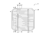
- FIG. 2 is a plan view of the solar cell 11 applied to the solar cell module 10 as seen from the light receiving surface side.
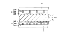
- FIG. 3 is a diagram showing a part of a cross section taken along line AA of FIG.
- the solar cell module 10 includes a plurality of solar cells 11, a first protective member 12 disposed on the light receiving surface side of the solar cell 11, and a second protective member 13 disposed on the back surface side of the solar cell 11.
- the plurality of solar cells 11 are sandwiched between the first protective member 12 and the second protective member 13 and sealed with the filler 14.
- the solar cell module 10 further includes a wiring member 15 that electrically connects the solar cells 11 to each other. Moreover, the solar cell module 10 is normally provided with the transition wiring material which connects the wiring materials 15 mutually, a flame
- the solar cell 11 includes a photoelectric conversion unit 20 that generates carriers by receiving sunlight, a first electrode 30 that is a light-receiving surface electrode formed on the light-receiving surface of the photoelectric conversion unit 20, and the photoelectric conversion unit 20. And a second electrode 40 that is a back electrode formed on the back surface.
- carriers generated by the photoelectric conversion unit 20 are collected by the first electrode 30 and the second electrode 40.
- the “light receiving surface” means a surface on which sunlight mainly enters from the outside of the solar cell 11
- the “back surface” means a surface opposite to the light receiving surface. For example, more than 50% to 100% of the sunlight incident on the solar cell 11 enters from the light receiving surface side.
- the photoelectric conversion unit 20 includes a substrate 21 made of a semiconductor material such as crystalline silicon (c-Si), gallium arsenide (GaAs), indium phosphide (InP), and an amorphous semiconductor formed on the light receiving surface of the substrate 21.
- a layer 22 and an amorphous semiconductor layer 23 formed on the back surface of the substrate 21 are included.
- the amorphous semiconductor layer 22 has a layer structure in which, for example, an i-type amorphous silicon layer and a p-type amorphous silicon layer are sequentially formed.
- the amorphous semiconductor layer 23 has a layer structure in which, for example, an i-type amorphous silicon layer and an n-type amorphous silicon layer are sequentially formed.
- an i-type amorphous silicon layer and an n-type amorphous silicon layer are sequentially formed on the light receiving surface of the substrate 21, and the i-type amorphous silicon is formed on the back surface of the substrate 21.
- a structure in which a layer and a p-type amorphous silicon layer are sequentially formed may be employed.
- the first electrode 30 and the second electrode 40 include transparent conductive layers 31 and 41, respectively.
- the transparent conductive layers 31 and 41 are made of, for example, a transparent conductive oxide obtained by doping metal oxide such as indium oxide (In 2 O 3 ) or zinc oxide (ZnO) with tin (Sn) or antimony (Sb). Composed.
- the transparent conductive layers 31 and 41 are preferably formed on the amorphous semiconductor layers 22 and 23 so as to cover the entire region excluding the edge portions.
- the first electrode 30 further includes a plurality of (for example, 50) finger electrodes 32 formed on the transparent conductive layer 31 as a collecting electrode for collecting carriers via the transparent conductive layer 31, and a plurality of (for example, 2) Book) bus bar electrode 33.
- the finger electrode 32 is a fine wire electrode formed over a wide area on the transparent conductive layer 31.
- the bus bar electrode 33 is an electrode that collects carriers from the finger electrodes 32.
- each bus-bar electrode 33 is arrange
- the plurality of finger electrodes 32 are arranged so that a part thereof extends from each of the bus bar electrodes 33 toward the edge of the light receiving surface, and the remaining part connects the bus bar electrodes 33.
- the second electrode 40 includes a plurality (for example, 250) of finger electrodes 42 and a plurality (for example, two) of bus bar electrodes 43 formed on the transparent conductive layer 41. Including. The arrangement of each electrode is the same as that of the first electrode 30.
- the finger electrodes 32 and 42 and the bus bar electrodes 33 and 43 have, for example, a structure in which conductive fillers are dispersed in a binder resin.
- conductive fillers for example, metal particles such as silver (Ag), copper (Cu), nickel (Ni), carbon, or a mixture thereof is used. Of these, Ag particles are preferred.
- the collector electrode is formed by, for example, a screen printing method using a conductive paste.
- the collector electrode can also be formed by an electrolytic plating method.
- the width of the finger electrode 32 is preferably about 30 ⁇ m to 150 ⁇ m, more preferably about 40 ⁇ m to 100 ⁇ m, from the viewpoint of reducing the light shielding loss.
- the width of the bus bar electrode 33 is preferably about 50 ⁇ m to 300 ⁇ m, and more preferably about 80 ⁇ m to 150 ⁇ m.
- the height of the finger electrode 32 and the bus bar electrode 33 (the length from the texture structure convex portion to the uppermost surface of each electrode) is 40 ⁇ m to 150 ⁇ m from the viewpoint of reducing resistance loss and the like, and should be similar to each other. Is preferred.
- About the finger electrode 42 of the 2nd electrode 40 it is suitable to make a width
- the first protective member 12 for example, a light-transmitting member such as a glass substrate, a resin substrate, or a resin film can be used, but a glass substrate is preferable from the viewpoint of durability and the like.
- a resin substrate or a resin film made of polyethylene terephthalate (PET) or the like is preferable from the viewpoint of cost reduction or weight reduction. It is.
- the second protective member 13 may be an opaque substrate or a resin film, for example, a laminated base material laminated with an aluminum foil.
- the filler 14 it is preferable to use a resin such as ethylene vinyl acetate copolymer (EVA) from the viewpoint of adhesion to the solar cell 11 and the wiring material 15.
- EVA ethylene vinyl acetate copolymer
- Wiring material 15 connects solar cells 11 arranged adjacent to each other.
- One end side of the wiring member 15 is attached to the first electrode 30 of one solar cell 11 among the solar cells 11 arranged adjacent to each other.
- the other end side of the wiring member 15 is connected to the second electrode 40 of the other solar cell 11.
- the wiring member 15 is bent in the thickness direction of the solar cell module 10 between the adjacent solar cells 11, and connects the adjacent solar cells 11 in series.
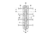
- FIG. 4 is an enlarged view of a portion B in FIG. In the figure, for the sake of clarity, only the outline of the wiring member 15 is indicated by a two-dot chain line.
- 5 and 6 are views showing a part of a cross section taken along the line CC of FIG. 4, and show the light receiving surface side and the back surface side, respectively.
- the wiring member 15 is attached on the first electrode 30 and the second electrode 40 using the adhesive 16.
- the adhesive 16 for example, it is preferable to use a thermosetting adhesive in which a curing agent is mixed with an epoxy resin, an acrylic resin, a urethane resin, or the like as necessary.
- a resin may contain a conductive filler such as Ag particles, but a non-conductive thermosetting adhesive is suitable from the viewpoint of manufacturing cost, light-shielding loss reduction, and the like.
- Examples of the form of the adhesive 16 include a film shape and a paste shape.
- the wiring member 15 is provided on the bus bar electrode 33 along the longitudinal direction of the bus bar electrode 33 extending linearly.
- the wiring member 15 also has a shape extending linearly, and the wiring member 15 is arranged in a state where the center portion in the width direction coincides with the center portion in the width direction of the bus bar electrode 33.
- the width W 15 of the wiring member 15 is preferably narrower from the viewpoint of reducing the light-shielding loss, but at least about 0.5 mm to 2.0 mm is necessary because mechanical strength that is not cut at the time of manufacture or use is necessary. It is preferably about 0.8 mm to 1.5 mm.
- the width W 15 of the wiring member 15 is wider than the width W 33 of the bus bar electrode 33, and W 15 / W 32 is preferably about 2 to 15 times, more preferably about 5 to 10 times.
- the wiring member 15 is attached so as to protrude from both sides of the bus bar electrode 33 in the width direction. For this reason, the wiring member 15 is also attached to a portion of the finger electrode 32 that is close to the bus bar electrode 33.
- the wiring member 15 has irregularities 15r on the surface facing the first protective member 12 side.
- the unevenness 15r has a function of diffusing light irradiated on the wiring material 15. Since the light diffused by the unevenness 15r is reflected again to the solar cell 11 side by the first protective member 12, the light receiving efficiency of the solar cell 11 can be increased.
- the unevenness height of the unevenness 15r (the length along the thickness direction from the concave portion to the convex portion) is preferably about 10 ⁇ m to 50 ⁇ m. Note that the surface of the wiring member 15 facing the second protective member 13 side is flat without the irregularities 15r. For this reason, the wiring material 15 has a flat surface facing the bus bar electrode 33, and has unevenness 15 r on the surface facing the bus bar electrode 43.
- the adhesive 16 is provided in the region R immediately below the wiring material 15. Specifically, it is provided between the wiring member 15 and the collector electrode and between the wiring member 15 and the photoelectric conversion unit 20. A small amount of the adhesive 16 is interposed between the wiring member 15 and the collector electrode of the first electrode 30, and the thickness thereof is about several nm to several hundred nm. There is more adhesive 16 interposed between the wiring member 15 and the collector electrode of the second electrode 40 than on the first electrode 30 side. This is due to the unevenness 15r of the wiring member 15, and the adhesive 16 is preferably provided so as to fill the concave portion of the unevenness 15r.
- the adhesive 16 is further provided so as to protrude from the region R immediately below and adhere to the side surface 15 s of the wiring member 15.
- the “side surface 15 s” is a surface along the thickness direction of the wiring material 15. That is, a fillet 16f (a portion with dots in FIG. 4) that protrudes from the region R immediately below the adhesive 16 is formed in the connection form between the wiring member 15 and the collector electrode.
- the fillet 16f is formed, for example, by pressing the adhesive 16 from the region R immediately below when the wiring member 15 is thermocompression bonded.
- the fillets 16 f are preferably formed on both sides of the wiring material 15 in the width direction along the edge of the wiring material 15.
- the fillet 16f covers a part of the side surface 15s of the wiring member 15, and directly bonds the side surface 15s to the light receiving surface and the back surface of the photoelectric conversion unit 20.
- the adhesive force can be increased as compared with the case where the wiring member 15 is bonded only in the region R immediately below. Further, it is possible to prevent the filler 14 from entering the region R immediately below.
- the width of the fillet 16f is preferably about 50 ⁇ m to 300 ⁇ m, for example, when the adhesive 16 does not have a light shielding property. On the other hand, when the adhesive 16 has a light shielding property, it is preferably narrower.
- the solar cell module 10 has a gap 17 in the region R immediately below the wiring member 15.
- a plurality of the gaps 17 exist in the region R immediately below, and are formed, for example, by introducing air into the adhesive 16 or introducing air between the adhesive 16 and the collector electrode. It can be said that the gap 17 is formed in the adhesive 16 because the periphery thereof is surrounded by the adhesive 16.
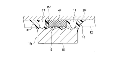
- the gap 17 can be confirmed by observing the adhesive 16 using an electron microscope (SEM) after peeling the wiring member 15 from the collector electrode. After the wiring material 15 is peeled off, the SEM image when the adhesive 16 is observed in a plan view looks like FIG.
- SEM electron microscope
- the gap 17 has a function of absorbing the stress generated by the thermal expansion of the adhesive 16 and the contraction accompanying it, and mitigating the influence. Thereby, peeling in the contact interface (The interface of the wiring material 15 and the adhesive agent 16, the interface of the adhesive agent 16 and the collector electrode) of the wiring material 15 and the collector electrode can be suppressed. Moreover, the space
- the void 17 is preferably provided in the region R immediately below, but may be present in the fillet 16f.
- the gaps 17 are formed between the wiring member 15 and the photoelectric conversion unit 20 in the region R immediately below.
- the gap 17 has, for example, a substantially circular shape in plan view, and its size (diameter) is preferably about 40 ⁇ m to 150 ⁇ m.
- the gap 17 includes, for example, one that communicates from the wiring member 15 to the photoelectric conversion unit 20.
- the void 17 is formed along the edge of the bus bar electrodes 33 and 43 in the region R immediately below.
- a plurality of gaps 17 are formed in a row along the edges of the bus bar electrodes 33 and 43.
- the gaps 17 are formed at the edges of the bus bar electrodes 33 and 43 at a higher density than in other regions.
- the edges of the bus bar electrodes 33 and 43 mean that the distance from the electrode end is within the range of the electrode widths W 33 and W 43 . That is, the density of the gaps 17 is higher on the width direction center part side than the width direction both ends of the region R directly below. Thereby, high adhesive force is expressed in the vicinity of both ends in the width direction of the region R immediately below including the fillet 16f portion while sufficiently reducing the influence of the volume change of the adhesive 16.
- more gaps 17 are formed between the wiring member 15 and the collector electrode on the back surface side than on the light receiving surface side.
- a gap 17 is formed only on the back surface side between the wiring member 15 and the collector electrode. This is due to the unevenness 15 r of the wiring member 15, and a gap 17 is formed between the concave portion of the unevenness 15 r and the collector electrode of the second electrode 40. Thereby, the effect of stress relaxation on the back side becomes remarkable, and the warpage of the solar cell 11 can be suppressed.
- the second electrode 40 has more metal particle components than the first electrode 30, and therefore stress is increased on the back surface side rather than the light receiving surface side of the solar cell 11.
- the bus bar electrode 33 may extend while repeating unevenness and have a zigzag shape in plan view. Also in this case, the gap 17 is provided along the edge of the bus bar electrode 33 in the region R immediately below the wiring member 15. Further, the adhesive 16 protrudes from the region R immediately below, and a fillet 16f is formed.
- FIGS. 8 and 9 are referred to in order to explain the process of attaching the wiring member 15.
- 8 and 9 are cross-sectional views showing a process of providing the adhesive 16 on the collecting electrode of the first electrode 30 and introducing the gap 17 into the region R immediately below (the same applies to the second electrode 40 side).
- the solar cell module 10 can be manufactured through a laminating process in which the constituent members are laminated and thermocompression bonded.
- the filler 14 is supplied in the form of a film having a thickness of about 0.1 mm to 1.0 mm, for example.
- the solar cell 11 is manufactured by a known method.
- the wiring member 15 is attached on the first electrode 30 and the second electrode 40 of the solar cell 11 using the adhesive 16, and the solar cells 11 arranged adjacent to each other are connected in series. In this way, a string of solar cells 11 is produced.
- the adhesive 16 for example, an adhesive made of a thermosetting resin in the form of a film or a paste can be used.
- FIG. 8 shows a case where the wiring material 15 is attached using a film-like adhesive 16.
- a film-like adhesive 16 wider than the bus bar electrode 33 is disposed on the collector electrode.
- heat treatment is performed while pressing the adhesive 16 with a cushioning member from this state, and the adhesive 16 is shaped so as to follow the shape of the bus bar electrode 33.
- such a member is not used.
- FIG.8 (b) it processes so that air may be embraced between the adhesive agent 16, the photoelectric conversion part 20, and a collector electrode.
- An example of such a processing method is a method of pressing the adhesive 16 using a flat and highly rigid plate.
- the adhesive 16 may be softened by applying hot air, and the both sides of the adhesive 16 may be hung down by its own weight.
- the heat treatment is performed at a temperature at which the adhesive 16 is softened and does not harden.
- FIG. 9 shows a case where the wiring material 15 is attached using the paste adhesive 16.
- gap 17 is used. Then, the adhesive 16 is applied onto the bus bar electrode 33 by a dispenser or the like.
- the paste-like adhesive 16 containing air 17z can be adjusted by, for example, stirring the paste whose viscosity is adjusted to the extent that it can be applied and capable of holding the air 17z. The adjusted adhesive 16 is applied without performing a deaeration process.
- the wiring material 15 is placed on the adhesive 16 processed or coated as described above and thermocompression bonded.
- the heating temperature is set to a temperature at which the adhesive 16 is cured.
- a part of the adhesive 16 existing in the immediately lower region R is pushed out from the immediately lower region R, and the fillet 16f is formed.
- a part of the gap 17 may be filled with the adhesive 16 until the adhesive 16 is cured.
- the usage amount (weight) of the adhesive 16 and the thermocompression bonding conditions are the same, the larger the introduction amount of the gap 17, the easier the adhesive 16 is pushed out from the region R immediately below, and the fillet 16 f is easily formed. That is, according to this manufacturing process, the shape of the fillet 16f can be adjusted by adjusting the introduction amount of the gaps 17.
- the 1st resin film which comprises the filler 14 is laminated
- the 2nd resin film which comprises the filler 14 is laminated
- a structure in which the strings of the solar cells 11 are sealed with the filler 14 is obtained.
- the solar cell module 10 is manufactured by attaching a frame and a terminal box.
- the solar cell module 10 has the gap 17 in the region R immediately below the wiring member 15, and has the fillet 16 f that directly bonds the side surface 15 s and the photoelectric conversion unit 20 along the edge of the wiring member 15. .
- the gap 17 absorbs the stress generated by the thermal expansion of the adhesive 16 and the shrinkage associated therewith, and suppresses the peeling of the adhesive interface.
- By providing the fillet 16f it is possible to increase the adhesive force as compared with the case of bonding only in the region R directly below the wiring member 15.
- the shape of the fillet 16 f can be easily controlled by the gap 17.
- the width of the fillet 16f can be widened while reducing the amount of the adhesive 16 used by increasing the amount of the gap 17 introduced. If the introduction amount of the gap 17 is reduced, the width of the fillet 16f can be reduced.
- the fillet 16f and the like can increase the adhesive force at the end of the region R directly below, and can prevent the filler 14 from entering the region R directly below.
- peeling of the wiring material 15 is promoted due to thermal expansion of the filler 14 or the like, but according to the bonding form, such a situation can be prevented.
- the solar cell module 10 it is possible to maintain good connectivity between the wiring member 15 and the collector electrode.
- a wiring material that does not have the unevenness 15r may be used.
- a metal layer formed over the entire area on the transparent conductive layer 41 may be provided.
- a structure other than the above may be applied to the photoelectric conversion unit.
- an i-type amorphous silicon layer 52 and an n-type amorphous silicon layer 53 are sequentially formed on the light-receiving surface side of a substrate 51 made of n-type single crystal silicon or the like.
- On the back side it is composed of a p-type region composed of an i-type amorphous silicon layer 54 and a p-type amorphous silicon layer 55, and an i-type amorphous silicon layer 56 and an n-type amorphous silicon layer 57.
- region may be sufficient.
- an electrode is provided only on the back side of the substrate 51.
- the electrode includes a p-side collector electrode 58 formed on the p-type region and an n-side collector electrode 59 formed on the n-type region.
- a transparent conductive layer 60 is formed between the p-type region and the p-side collector electrode 58 and between the n-type region and the n-side collector electrode 59.
- An insulating layer 61 is formed between the p-type region and the n-type region.
- the wiring members 15 are attached on the p-side collector electrode 58 and the n-side collector electrode 59, respectively. Further, as shown in FIG.
- membrane 73 may be sufficient.
Landscapes
- Photovoltaic Devices (AREA)
- Life Sciences & Earth Sciences (AREA)
- Engineering & Computer Science (AREA)
- Sustainable Energy (AREA)
- Sustainable Development (AREA)
Priority Applications (5)
| Application Number | Priority Date | Filing Date | Title |
|---|---|---|---|
| JP2014505948A JP6015973B2 (ja) | 2012-03-23 | 2012-03-23 | 太陽電池モジュール及びその製造方法 |
| EP12871962.2A EP2830101A4 (fr) | 2012-03-23 | 2012-03-23 | Module de pile solaire et son procédé de fabrication |
| CN201280071605.9A CN104221160B (zh) | 2012-03-23 | 2012-03-23 | 太阳电池组件及其制造方法 |
| PCT/JP2012/057596 WO2013140623A1 (fr) | 2012-03-23 | 2012-03-23 | Module de pile solaire et son procédé de fabrication |
| US14/477,996 US9691913B2 (en) | 2012-03-23 | 2014-09-05 | Solar cell module and method for manufacturing same |
Applications Claiming Priority (1)
| Application Number | Priority Date | Filing Date | Title |
|---|---|---|---|
| PCT/JP2012/057596 WO2013140623A1 (fr) | 2012-03-23 | 2012-03-23 | Module de pile solaire et son procédé de fabrication |
Related Child Applications (1)
| Application Number | Title | Priority Date | Filing Date |
|---|---|---|---|
| US14/477,996 Continuation US9691913B2 (en) | 2012-03-23 | 2014-09-05 | Solar cell module and method for manufacturing same |
Publications (1)
| Publication Number | Publication Date |
|---|---|
| WO2013140623A1 true WO2013140623A1 (fr) | 2013-09-26 |
Family
ID=49222114
Family Applications (1)
| Application Number | Title | Priority Date | Filing Date |
|---|---|---|---|
| PCT/JP2012/057596 Ceased WO2013140623A1 (fr) | 2012-03-23 | 2012-03-23 | Module de pile solaire et son procédé de fabrication |
Country Status (5)
| Country | Link |
|---|---|
| US (1) | US9691913B2 (fr) |
| EP (1) | EP2830101A4 (fr) |
| JP (1) | JP6015973B2 (fr) |
| CN (1) | CN104221160B (fr) |
| WO (1) | WO2013140623A1 (fr) |
Cited By (4)
| Publication number | Priority date | Publication date | Assignee | Title |
|---|---|---|---|---|
| WO2016157684A1 (fr) * | 2015-03-30 | 2016-10-06 | パナソニックIpマネジメント株式会社 | Module de cellules solaires |
| WO2017010385A1 (fr) * | 2015-07-10 | 2017-01-19 | 日東電工株式会社 | Module solaire, procédé de fabrication de module solaire, et procédé de câblage de cellule solaire |
| CN106784100A (zh) * | 2015-10-08 | 2017-05-31 | Lg电子株式会社 | 太阳能电池模块 |
| WO2017150372A1 (fr) * | 2016-02-29 | 2017-09-08 | パナソニックIpマネジメント株式会社 | Module de batterie solaire et procédé de fabrication de module de batterie solaire |
Citations (9)
| Publication number | Priority date | Publication date | Assignee | Title |
|---|---|---|---|---|
| JP2000261012A (ja) * | 1999-03-09 | 2000-09-22 | Mitsubishi Electric Corp | 太陽電池 |
| JP2005159173A (ja) * | 2003-11-27 | 2005-06-16 | Kyocera Corp | 太陽電池素子接続用配線材および太陽電池モジュール |
| JP2008053681A (ja) * | 2006-03-27 | 2008-03-06 | Kyocera Corp | 太陽電池モジュール及びその製造方法 |
| JP2008205137A (ja) | 2007-02-19 | 2008-09-04 | Sanyo Electric Co Ltd | 太陽電池及び太陽電池モジュール |
| WO2008139994A1 (fr) * | 2007-05-09 | 2008-11-20 | Hitachi Chemical Company, Ltd. | Élément de liaison conducteur, structure de liaison et module de cellule solaire |
| WO2009041506A1 (fr) * | 2007-09-26 | 2009-04-02 | Hitachi Chemical Company, Ltd. | Elément pour la connexion d'un conducteur, procédé pour fabriquer cet élément, structure de connexion et module de cellule solaire |
| JP2009081217A (ja) * | 2007-09-25 | 2009-04-16 | Sanyo Electric Co Ltd | 太陽電池モジュール |
| WO2010122875A1 (fr) * | 2009-04-21 | 2010-10-28 | 三洋電機株式会社 | Module de cellule solaire |
| WO2011013814A2 (fr) * | 2009-07-30 | 2011-02-03 | 三洋電機株式会社 | Module à cellules solaires |
Family Cites Families (9)
| Publication number | Priority date | Publication date | Assignee | Title |
|---|---|---|---|---|
| US20070235077A1 (en) | 2006-03-27 | 2007-10-11 | Kyocera Corporation | Solar Cell Module and Manufacturing Process Thereof |
| US20080011347A1 (en) * | 2006-07-14 | 2008-01-17 | Hitachi Cable, Ltd. | Connecting lead wire for a solar battery module, method for fabricating same, and solar battery module using the connecting lead wire |
| JP5230089B2 (ja) * | 2006-09-28 | 2013-07-10 | 三洋電機株式会社 | 太陽電池モジュール |
| JP5121203B2 (ja) * | 2006-09-29 | 2013-01-16 | 三洋電機株式会社 | 太陽電池モジュール |
| JP4463297B2 (ja) * | 2007-08-07 | 2010-05-19 | 三洋電機株式会社 | 太陽電池モジュール |
| JP2009158858A (ja) * | 2007-12-27 | 2009-07-16 | Sanyo Electric Co Ltd | 太陽電池モジュール及びその製造方法 |
| JP5147672B2 (ja) * | 2008-01-31 | 2013-02-20 | 三洋電機株式会社 | 太陽電池モジュール及び太陽電池モジュールの製造方法 |
| WO2009107804A1 (fr) * | 2008-02-28 | 2009-09-03 | 三洋電機株式会社 | Module de cellule solaire |
| JP4948458B2 (ja) | 2008-03-19 | 2012-06-06 | 三洋電機株式会社 | 太陽電池の製造方法及び太陽電池 |
-
2012
- 2012-03-23 WO PCT/JP2012/057596 patent/WO2013140623A1/fr not_active Ceased
- 2012-03-23 JP JP2014505948A patent/JP6015973B2/ja active Active
- 2012-03-23 EP EP12871962.2A patent/EP2830101A4/fr not_active Withdrawn
- 2012-03-23 CN CN201280071605.9A patent/CN104221160B/zh active Active
-
2014
- 2014-09-05 US US14/477,996 patent/US9691913B2/en active Active
Patent Citations (9)
| Publication number | Priority date | Publication date | Assignee | Title |
|---|---|---|---|---|
| JP2000261012A (ja) * | 1999-03-09 | 2000-09-22 | Mitsubishi Electric Corp | 太陽電池 |
| JP2005159173A (ja) * | 2003-11-27 | 2005-06-16 | Kyocera Corp | 太陽電池素子接続用配線材および太陽電池モジュール |
| JP2008053681A (ja) * | 2006-03-27 | 2008-03-06 | Kyocera Corp | 太陽電池モジュール及びその製造方法 |
| JP2008205137A (ja) | 2007-02-19 | 2008-09-04 | Sanyo Electric Co Ltd | 太陽電池及び太陽電池モジュール |
| WO2008139994A1 (fr) * | 2007-05-09 | 2008-11-20 | Hitachi Chemical Company, Ltd. | Élément de liaison conducteur, structure de liaison et module de cellule solaire |
| JP2009081217A (ja) * | 2007-09-25 | 2009-04-16 | Sanyo Electric Co Ltd | 太陽電池モジュール |
| WO2009041506A1 (fr) * | 2007-09-26 | 2009-04-02 | Hitachi Chemical Company, Ltd. | Elément pour la connexion d'un conducteur, procédé pour fabriquer cet élément, structure de connexion et module de cellule solaire |
| WO2010122875A1 (fr) * | 2009-04-21 | 2010-10-28 | 三洋電機株式会社 | Module de cellule solaire |
| WO2011013814A2 (fr) * | 2009-07-30 | 2011-02-03 | 三洋電機株式会社 | Module à cellules solaires |
Non-Patent Citations (1)
| Title |
|---|
| See also references of EP2830101A4 |
Cited By (7)
| Publication number | Priority date | Publication date | Assignee | Title |
|---|---|---|---|---|
| WO2016157684A1 (fr) * | 2015-03-30 | 2016-10-06 | パナソニックIpマネジメント株式会社 | Module de cellules solaires |
| JPWO2016157684A1 (ja) * | 2015-03-30 | 2017-11-02 | パナソニックIpマネジメント株式会社 | 太陽電池モジュール |
| US10879410B2 (en) | 2015-03-30 | 2020-12-29 | Panasonic Intellectual Property Management Co., Ltd. | Solar cell module |
| WO2017010385A1 (fr) * | 2015-07-10 | 2017-01-19 | 日東電工株式会社 | Module solaire, procédé de fabrication de module solaire, et procédé de câblage de cellule solaire |
| CN106784100A (zh) * | 2015-10-08 | 2017-05-31 | Lg电子株式会社 | 太阳能电池模块 |
| WO2017150372A1 (fr) * | 2016-02-29 | 2017-09-08 | パナソニックIpマネジメント株式会社 | Module de batterie solaire et procédé de fabrication de module de batterie solaire |
| JPWO2017150372A1 (ja) * | 2016-02-29 | 2018-10-25 | パナソニックIpマネジメント株式会社 | 太陽電池モジュールおよび太陽電池モジュールの製造方法 |
Also Published As
| Publication number | Publication date |
|---|---|
| JP6015973B2 (ja) | 2016-10-26 |
| JPWO2013140623A1 (ja) | 2015-08-03 |
| CN104221160B (zh) | 2016-10-26 |
| EP2830101A1 (fr) | 2015-01-28 |
| US9691913B2 (en) | 2017-06-27 |
| CN104221160A (zh) | 2014-12-17 |
| US20150083185A1 (en) | 2015-03-26 |
| EP2830101A4 (fr) | 2015-04-08 |
Similar Documents
| Publication | Publication Date | Title |
|---|---|---|
| KR101535297B1 (ko) | 태양 전지 모듈 | |
| JP4294048B2 (ja) | 太陽電池モジュール | |
| CN102414829B (zh) | 太阳能电池模块 | |
| JP5367588B2 (ja) | 太陽電池モジュール | |
| KR20100036315A (ko) | 태양 전지 모듈의 제조 방법 | |
| JP2009267270A (ja) | 太陽電池モジュール | |
| JP2009246108A (ja) | 太陽電池モジュール | |
| US20180145192A1 (en) | Solar cell module production method | |
| EP2579324B1 (fr) | Module de cellules solaires et son procédé de fabrication | |
| CN110190145A (zh) | 背接触叠片太阳电池串及制造方法、叠片太阳电池组件 | |
| JP6015973B2 (ja) | 太陽電池モジュール及びその製造方法 | |
| JP2009238959A (ja) | 圧着装置及び太陽電池モジュールの製造方法 | |
| JP2008294366A (ja) | 太陽電池モジュール | |
| US20140190547A1 (en) | Solar cell module, and method for manufacturing solar cell module | |
| WO2011108634A1 (fr) | Module de cellule solaire | |
| JP2009218315A (ja) | 太陽電池モジュール | |
| US20140083499A1 (en) | Solar module and manufacturing method therefor | |
| JP6249304B2 (ja) | 太陽電池モジュール | |
| JP2011222744A (ja) | 太陽電池接続用タブ線、接続方法、及び太陽電池モジュール | |
| US20150083187A1 (en) | Solar cell module and solar cell module manufacturing method | |
| JP5381809B2 (ja) | 太陽電池モジュール | |
| JP2020155684A (ja) | 太陽電池ストリング、太陽電池モジュール、太陽電池セルの製造方法 | |
| JP5934985B2 (ja) | 太陽電池モジュールの製造方法及び太陽電池モジュール | |
| JP6083685B2 (ja) | 太陽電池モジュール及び太陽電池モジュールの製造方法 | |
| JP5382150B2 (ja) | 太陽電池モジュール |
Legal Events
| Date | Code | Title | Description |
|---|---|---|---|
| 121 | Ep: the epo has been informed by wipo that ep was designated in this application |
Ref document number: 12871962 Country of ref document: EP Kind code of ref document: A1 |
|
| ENP | Entry into the national phase |
Ref document number: 2014505948 Country of ref document: JP Kind code of ref document: A |
|
| WWE | Wipo information: entry into national phase |
Ref document number: 2012871962 Country of ref document: EP |
|
| NENP | Non-entry into the national phase |
Ref country code: DE |