WO2017010385A1 - Module solaire, procédé de fabrication de module solaire, et procédé de câblage de cellule solaire - Google Patents
Module solaire, procédé de fabrication de module solaire, et procédé de câblage de cellule solaire Download PDFInfo
- Publication number
- WO2017010385A1 WO2017010385A1 PCT/JP2016/070070 JP2016070070W WO2017010385A1 WO 2017010385 A1 WO2017010385 A1 WO 2017010385A1 JP 2016070070 W JP2016070070 W JP 2016070070W WO 2017010385 A1 WO2017010385 A1 WO 2017010385A1
- Authority
- WO
- WIPO (PCT)
- Prior art keywords
- coating layer
- layer
- solar cell
- meth
- solar
- Prior art date
- Legal status (The legal status is an assumption and is not a legal conclusion. Google has not performed a legal analysis and makes no representation as to the accuracy of the status listed.)
- Ceased
Links
Images








Classifications
-
- H—ELECTRICITY
- H10—SEMICONDUCTOR DEVICES; ELECTRIC SOLID-STATE DEVICES NOT OTHERWISE PROVIDED FOR
- H10F—INORGANIC SEMICONDUCTOR DEVICES SENSITIVE TO INFRARED RADIATION, LIGHT, ELECTROMAGNETIC RADIATION OF SHORTER WAVELENGTH OR CORPUSCULAR RADIATION
- H10F19/00—Integrated devices, or assemblies of multiple devices, comprising at least one photovoltaic cell covered by group H10F10/00, e.g. photovoltaic modules
- H10F19/90—Structures for connecting between photovoltaic cells, e.g. interconnections or insulating spacers
-
- Y—GENERAL TAGGING OF NEW TECHNOLOGICAL DEVELOPMENTS; GENERAL TAGGING OF CROSS-SECTIONAL TECHNOLOGIES SPANNING OVER SEVERAL SECTIONS OF THE IPC; TECHNICAL SUBJECTS COVERED BY FORMER USPC CROSS-REFERENCE ART COLLECTIONS [XRACs] AND DIGESTS
- Y02—TECHNOLOGIES OR APPLICATIONS FOR MITIGATION OR ADAPTATION AGAINST CLIMATE CHANGE
- Y02E—REDUCTION OF GREENHOUSE GAS [GHG] EMISSIONS, RELATED TO ENERGY GENERATION, TRANSMISSION OR DISTRIBUTION
- Y02E10/00—Energy generation through renewable energy sources
- Y02E10/50—Photovoltaic [PV] energy
Definitions
- the present invention relates to a solar cell module, a method for manufacturing a solar cell module, and a method for wiring solar cells.
- This application includes Japanese Patent Application No. 2015-139211 filed on July 10, 2015, Japanese Patent Application No. 2015-218976 filed on November 6, 2015, and March 18, 2016. Claims priority based on the filed Japanese Patent Application No. 2016-054790, the entire contents of which are incorporated herein by reference.
- Solar cell modules that convert light energy into electric power are widely used as clean power generators.
- the solar cell module includes a solar cell and a wiring connected to the cell, and the power generated in the cell through the wiring is configured to be supplied to the outside.
- Patent documents 1 to 8 are cited as documents disclosing this type of prior art.
- Patent Documents 1 to 6 relate to a solar cell module in which an n-type electrode is partially disposed on the front surface side of the solar battery cell and a p-type electrode is disposed on the back surface side.
- the present invention relates to a solar cell module that employs a back contact method in which both electrodes are arranged on the back side.
- the structures disclosed in Patent Documents 1 and 2 require that the wiring of solar cells must be individually joined using solder etc. It takes time and there is a limit to improving productivity.
- heating is performed at the time of bonding, such as solder bonding, the characteristics of the cell may be reduced by heating, or the cell may be warped or cracked.
- Solder joints also have a problem of flux contamination.
- the solar cell modules disclosed in Patent Documents 3 and 4 also have the same problems as Patent Documents 1 and 2 because the wires serving as the conductive paths are soldered. Moreover, the said wire is arrange
- the solar cell module described in Patent Document 5 is provided with a pair of sealing sheets having metal wiring on the surface, and sandwiching a plurality of solar cells with the pair of sealing sheets, the metal wiring and the solar cells. Are pressed and heated to electrically connect a plurality of solar cells without requiring solder bonding.
- the conduction between the upper and lower metal wirings includes factors such as securing the contact area and accuracy of alignment, and the conduction state (contact state) of the metal wirings may be impaired by the flow of the sealing resin or the like. is there. These cause deterioration in performance over time, that is, decrease in durability, as a reduction in current collection efficiency and wiring defects.
- Patent Document 6 although the connection reliability is improved by using a conductive film or the like for joining the upper and lower metal wirings, the joint point between the upper and lower metal wirings is a weak point in strength. There are structural limits to improving yield. Thus, with the conventional technical level, it was impossible to achieve both productivity and durability.
- the present invention has been created in view of the above circumstances, and an object thereof is to provide a solar cell module having excellent productivity and improved durability. Another related object is to provide a method for manufacturing such a solar cell module and a method for wiring solar cells.
- a solar cell module provided with a photovoltaic cell.
- This solar cell module includes a conductive portion.
- the conductive portion is partially disposed on the back surface of the solar battery cell.
- the solar cell module further includes a coating layer.
- the covering layer covers the back surface of the solar battery cell over the conductive portion and adheres to the back surface of the solar battery cell.
- the said coating layer is partially arrange
- the coating layer covering the conductive portion from the outside of the cell back surface favorably maintains the contact state between the cell back surface and the conductive portion.
- the coating layer covers the conductive part and is adhered to the back surface of the cell outside the conductive part, the presence of the coating layer makes it possible to use a sealing resin that is usually used for sealing solar cells. Events that adversely affect the contact state between the cell back surface and the conductive portion are prevented.
- the coating layer partially covers the cell back surface, there is a coating layer non-arranged region on the back surface. By providing the covering layer non-arrangement region, the durability of the solar cell module can be further improved as compared with the configuration without the covering layer non-arrangement region.
- the sealing resin usually used for sealing the solar battery cell flows and contacts the back surface of the solar battery cell in the coating layer non-arrangement region, and then adheres to the back surface of the cell by curing (curing adhesion) ) That is, by providing the coating layer non-arrangement region, the contact state between the cell back surface and the conductive portion can be further stabilized by utilizing the action such as the fixing of the sealing resin. As a result, the durability of the solar cell module is improved. ADVANTAGE OF THE INVENTION According to this invention, the solar cell module which is excellent in productivity and can improve durability is provided.
- wiring by contact between the front and back surfaces of the solar battery cell (more specifically, the front and back electrodes of the solar battery cell) and the conductive portion (for example, conductive wire), solder bonding or conductive May be referred to as “physical contact” to distinguish from bonding using bonding means such as adhesive (direct bonding means; also referred to as conductive bonding means; the same shall apply hereinafter).
- Physical contact refers to a contact state or a contact method in which conduction is achieved by contact only by contact without using an adhesive means.
- the coating layer disclosed here may have adhesiveness, it plays the role of assisting and holding the physical contact, and is understood to be different from the bonding means.
- the “solderless wiring” that does not use a low melting point metal such as solder as described above is a typical example of physical contact wiring.
- a solar cell module constructed by such physical contact type wiring is referred to as a physical contact type solar cell module. Since the physical contact type solar cell module can be conducted without heating, cell characteristics can be prevented from being deteriorated due to heating. Moreover, according to the solar cell module that performs solderless wiring (solderless solar cell module), not only the above-mentioned flux contamination can be avoided, but also problems such as leaching and cratering caused by solder bonding can be solved.
- the conductive portion is composed of a plurality of conductive wires.
- the coating layer is composed of a plurality of strip-shaped coating members. Further, in the back surface of the solar battery cell, one of the plurality of belt-shaped covering members covers one conductive wire of the plurality of conductive wires from the outside of the back surface of the solar battery cell, And it adhere
- the coating layer is an adhesive sheet.
- the cell back surface and the conductive portion (for example, a plurality of conductive wires) can be preferably kept conductive by physical contact using the pressure-sensitive adhesive properties of the pressure-sensitive adhesive sheet.
- the adhesive sheet adheres to the back surface of the cell on the outside of the conductive portion (for example, both outer sides of the plurality of conductive lines), and thus prevents, for example, the flow of the sealing resin toward the conductive portion, And the contact state between the conductive portion (for example, a plurality of conductive wires) are better maintained.
- the pressure-sensitive adhesive sheet is a substrate-less pressure-sensitive adhesive sheet comprising a pressure-sensitive adhesive layer.
- the pressure-sensitive adhesive sheet includes a base material layer and a pressure-sensitive adhesive layer disposed on at least one surface of the base material layer. By comprising in this way, the durability of the said wiring can be further improved using the rigidity of a base material layer, obtaining the wiring excellent in connection reliability using the adhesion characteristic by an adhesive layer. .
- a sealing resin is disposed on the back surface of the solar battery cell so as to cover the back surface through the coating layer.
- the sealing resin is bonded to the back surface of the solar battery cell in the coating layer non-arrangement region.
- the method of manufacturing a solar cell module includes: a step of partially disposing a conductive portion on a back surface of a solar cell; a step of adhering a covering layer to the back surface of the solar cell on which the conductive portion is disposed; including. Moreover, in the adhesion step of the covering layer, the covering layer is partially disposed on the back surface of the solar battery cell. According to said method, a solar cell module with high contact reliability can be efficiently produced using adhesion
- the wiring method of a photovoltaic cell includes: partially disposing a conductive portion on the back surface of the solar cell; adhering a coating layer over the conductive portion on the back surface of the solar cell on which the conductive portion is disposed; ;including. Moreover, in the adhesion step of the covering layer, the covering layer is partially disposed on the back surface of the solar battery cell. According to said method, the wiring of the photovoltaic cell excellent in durability can be efficiently implement
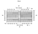
- FIG. 3 is a view in the direction of arrow III in FIG. 2.
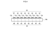
- FIG. 4 is a cross-sectional view taken along line IV-IV of the solar battery cell of FIG.
- It is typical sectional drawing which expands and shows the electroconductive part and coating layer in the photovoltaic cell lower surface which concerns on 2nd Embodiment.
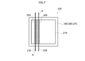
- It is a typical top view of the solar cell module for a test (reference example) used for the heat cycle test.
- 6 is a graph showing the results of a heat cycle test of Reference Example 1.
- 6 is a graph showing the results of a heat cycle test of Reference Example 2.
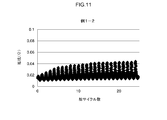
- 3 is a graph showing the results of a heat cycle test in Example 1-1. It is a graph which shows the result of the heat cycle test of Example 1-2.
- 6 is a graph showing the results of a heat cycle test in Example 2-1. It is a graph which shows the result of the heat cycle test of Example 2-2.
- FIG. 1 is a cross-sectional view schematically showing a main part of the solar cell module according to the first embodiment.
- a solar cell module 1 includes a plurality of solar cells including solar cells 10a, 10b, 10c, and 10d, a sealing resin 150 that covers (surrounds) the plurality of solar cells, and a sealing resin.
- the front surface covering member 160 and the back surface covering member 170 are disposed so as to sandwich the stop resin 150 therebetween.
- a plurality of solar cells including the solar cells 10a, 10b, 10c, and 10d are arranged in a straight line at a predetermined interval to constitute a solar cell group.
- n-type electrode front electrode
- p-type electrode rear surface
- lower surface back surface
- Electrode Electrode
- the upper and lower sides of the solar battery cell in this specification correspond to the front and back of the solar battery cell, and thus correspond to the front and back (upper and lower) of the solar battery module.
- the surface of the solar cell module is a light incident surface (also referred to as a light receiving surface).
- the top and bottom may not necessarily be strictly up and down, so the top and bottom of the solar cells are not limited to exact top and bottom, and are understood to indicate relative positional relationships.
- crystalline Si cells (approximately 15.6 cm ⁇ 15.6 cm) are used as the solar cells 10a, 10b, 10c, and 10d, and an ethylene-vinyl acetate copolymer (EVA) is used as the sealing resin 150.
- EVA ethylene-vinyl acetate copolymer
- a glass plate having a thickness of 3.2 mm is used as the surface covering member 160, and a commercially available back sheet is used as the back surface covering member 170.
- two adjacent solar cells (for example, the solar cell 10a and the solar cell 10b) are electrically connected by one conductive portion 30.
- One of the conductive portions 30 is partially disposed on the surface of the solar battery cell 10a, and extends from the upper surface of the solar battery cell 10a to the lower surface of the solar battery cell 10b.
- the conductive part 30 is also partially disposed on the back surface of the solar battery cell 10b. More specifically, the one conductive portion 30 is disposed on the upper surface of the solar battery cell 10a above the solar battery group, and passes through the space between the solar battery cell 10a and the solar battery cell 10b. It moves below the solar cell group and is disposed on the lower surface of the solar cell 10b.
- the conductive portion 30 extends from the end of the solar cell 10a (the end opposite to the solar cell 10b side) to the end of the solar cell 10b (the end opposite to the solar cell 10a side), It contacts (specifically abuts) the upper surface of the solar battery cell 10a and the lower surface of the solar battery cell 10b.
- the electroconductive part 30 is one member and continues from the upper surface of the solar cell 10a to the lower surface of the solar cell 10b, the connection reliability is high and the durability is also excellent.
- the first coating layer 50 is disposed above the solar cell group. Specifically, one first covering layer 50 is disposed only above one solar battery cell 10a, and is not disposed above another solar battery cell (for example, solar battery cell 10b). A different first covering layer 50 is disposed above another solar battery cell (for example, solar battery cell 10b). Moreover, the 1st coating layer 50 is arrange
- the 1st coating layer 50 is a transparent resin layer, and the surface at the side of a photovoltaic cell has adhesiveness at least.
- the 1st coating layer 50 of this embodiment is a transparent adhesive layer (base material-less adhesive sheet).
- the first covering layer 50 is in contact with the upper surface of the solar battery cell 10 a from above the conductive portion 30 in the non-existing region of the conductive portion 30.
- the conductive portion 30 is reliably and stably brought into contact (specifically, contacted) with the upper surface of the solar battery cell 10a. Details thereof will be described later.
- the first coating layer 50 is not limited to the adhesive layer, but is itself non-adhesive and adheres to the upper surface of the solar battery cell 10a using a known adhesive means such as an adhesive or a pressure-sensitive adhesive. You may do.
- the second coating layer 60 is disposed in the solar cell module 1 below the solar cell group. Specifically, one second covering layer 60 is disposed only below one solar battery cell 10b, and is disposed below other solar battery cells (for example, solar battery cells 10a and 10c). Absent. Different second coating layers 60 are arranged below other solar cells (for example, solar cells 10a and 10c). Moreover, the 2nd coating layer 60 is arrange
- the second coating layer 60 is a transparent pressure-sensitive adhesive layer (baseless pressure-sensitive adhesive sheet).
- the second coating layer 60 is in contact with the lower surface of the solar battery cell 10 b from below the conductive portion 30 in the non-existing region of the conductive portion 30. Thereby, the electroconductive part 30 is made to contact the lower surface of the photovoltaic cell 10b reliably and stably. Details thereof will be described later.
- positioned at the back surface of a photovoltaic cell does not need to be transparent.
- FIG. 2 is a schematic side view showing an enlarged wiring state of two solar cells constituting the solar cell module according to the first embodiment.
- 3 is a view in the direction of the arrow III in FIG.
- FIG. 4 is a cross-sectional view taken along the line IV-IV of the solar battery cell of FIG.
- the wiring in the solar battery module 1 will be described more specifically by taking the wiring of the solar battery cells 10a and 10b as an example. 2 to 4, for convenience of explanation, the conductive portion and the second covering layer disposed on the lower surface of the solar battery cell 10a, and the conductive portion and the first covering layer disposed on the upper surface of the solar battery cell 10b are shown. Omitted.
- one conductive portion 30 is composed of a plurality of conductive wires 40 extending from the upper surface of the solar battery cell 10a to the lower surface of the solar battery cell 10b.
- the plurality of conductive lines 40 extend along the arrangement direction of the solar cells 10a and 10b, and are arranged at intervals. These conductive wires 40 are arranged in a straight line so as to be parallel to each other.
- substantially both ends of the solar cells 10a and 10b ends of the solar cells 10a (solar cells) From the end opposite to the 10b side) to the end of the solar battery cell 10b (the end opposite to the solar battery 10a side).
- the plurality of conductive lines 40 are linearly arranged on the upper surface of the solar battery cell 10a and the lower surface of the solar battery cell 10b so as to be parallel to each other with a space therebetween.
- a copper wire having a width of 0.8 mm and a thickness of 0.25 mm is used as the conductive wire 40.
- the first coating layer 50 covers the plurality of conductive wires 40 as the conductive portion 30 and is bonded to the upper surface of the solar battery cell 10 a through the conductive portion 30. That is, the lower surface (the surface on the solar cell side) of the first coating layer 50 is bonded to the conductive portion 30 (specifically, the plurality of conductive wires 40) and is not bonded to the conductive portion 30. It adheres to the upper surface of the solar battery cell 10a. Thus, the conductive portion 30 is reliably and stably brought into contact (specifically, contacted) with the upper surface of the solar battery cell 10a. Moreover, the 1st coating layer 50 is partially arrange
- the coating layer non-arrangement region 12a exists on the upper surface of the solar battery cell 10a.
- the sealing resin 150 before curing flows into the coating layer non-arrangement region 12a and cures after contacting the upper surface of the solar battery cell 10a.
- the contact state between the solar battery cell 10a and the conductive portion 30 (specifically, the plurality of conductive wires 40) is more stable due to the adhesion by the first coating layer 50 and the fixing (curing adhesion) of the sealing resin 150.
- the conductive portion 30 does not exist in the coating layer non-arrangement region 12a.
- the first covering layer 50 includes a plurality of strip-shaped covering members 52.
- the number of these strip-shaped covering members 52 is the same as that of the conductive wires 40, and each of them is bonded to the upper surface of the solar battery cell 10a through the conductive wire 40 disposed on the upper surface of the solar battery cell 10a.
- the width of each band-shaped covering member 52 is larger than the width of the conductive wire 40.
- the length of each strip-shaped covering member 52 is substantially the same as the length of one side of the solar battery cell 10a.
- Each of the strip-shaped covering members 52 is linearly disposed on the upper surface of the solar battery cell 10a so as to overlap each conductive line 40 and to be parallel to each other.
- Each strip-shaped covering member 52 covers each of the conductive wires 40 arranged on the upper surface of the solar battery cell 10a from above (outside the upper surface) of the solar battery cell 10a, and the width of the conductive wire 40. It is bonded to the upper surface of the solar battery cell 10a on both outer sides in the direction. Further, the plurality of strip-shaped covering members 52 are arranged at intervals. Therefore, a strip-shaped coating layer non-arrangement region 12 a exists between the plurality of strip-shaped coating members 52. By arranging the first coating layer 50 in this way, a wiring excellent in connection reliability is preferably realized.
- the band-shaped covering member 52 constituting the first covering layer 50 is a transparent adhesive layer having a width of about 5 to 10 mm and a thickness of about 0.05 mm in this embodiment, but is not limited thereto.
- the width W1 of the strip-shaped covering member 52 is suitably 1 mm or more larger than the width Wc of the conductive wire 40.
- the difference (W1 ⁇ Wc) between W1 and the width Wc of the conductive wire 40 is preferably 2 mm or more, more preferably 3 mm or more (for example, 7 mm or more).
- the ratio (W1 / Wc) of the width W1 of the band-shaped covering member 52 to the width Wc of the conductive wire 40 is appropriately larger than 1, preferably 3 or more, more preferably 5 or more (for example, 10 Above). Further, from the viewpoint of durability, productivity, translucency, etc., the difference (W1 ⁇ Wc) is suitably about 20 mm or less, preferably 15 mm or less, more preferably 10 mm or less, and still more preferably. It is 7 mm or less (for example, 5 mm or less).
- the ratio (W1 / Wc) of the width W1 of the band-shaped covering member 52 to the width Wc of the conductive wire 40 is suitably 20 or less, preferably 15 or less (for example, 8 or less).
- the width W1 of the belt-shaped covering member 52 is suitably 1.5 mm or more, preferably 3 mm or more, more preferably 4 mm or more (for example, 8 mm or more), and the width W1 is It is suitable that it is 25 mm or less, preferably 18 mm or less, more preferably 12 mm or less (for example, 7 mm or less).
- the interval between the strip-shaped covering members 52 is preferably approximately the same as the interval between the conductive wires 40 arranged on the upper surface of the solar battery cell 10a, but is not limited thereto.
- the interval between the strip-shaped covering members 52 is preferably 0.3 cm or more, more preferably 0.8 cm or more, and further preferably 1.5 cm or more.
- the interval is preferably less than 4.0 cm, more preferably less than 3.0 cm, and even more preferably 2.8 cm or less.
- interval is a pitch and points the distance between the centerlines in the width direction of the strip
- the width of each of the strip-shaped coating layer non-arranged regions 12a existing between the strip-shaped coating members 52 of the first coating layer 50 is a viewpoint of improving durability. Accordingly, the thickness is suitably 1 mm or more, preferably 3 mm or more, more preferably 5 mm or more, still more preferably 8 mm or more, and particularly preferably 10 mm or more (for example, 12 mm or more, further 15 mm or more).
- the width of each of the band-shaped coating layer non-arrangement regions 12a is suitably about 25 mm or less, preferably about 22 mm or less (for example, 16 mm or less). It is.
- the area ratio of the coating layer non-arrangement region 12a on the upper surface of the solar battery cell is not limited to a specific ratio, and is appropriately about 10% or more and is durable. From the viewpoints of lightness and translucency, it is preferably 30% or more, more preferably 40% or more, still more preferably 50% or more, and particularly preferably 60% or more (for example, 70% or more). From the viewpoint of covering the conductive portion 30 with the first coating layer 50, the area ratio is suitably about 90% or less, preferably 85% or less (for example, 65% or less). In another aspect, the area ratio is preferably about 75% or less (for example, 70% or less), and may be 60% or less.
- the second covering layer 60 covers the plurality of conductive wires 40 as the conductive portion 30 and adheres to the lower surface of the solar battery cell 10b through the conductive portion 30. ing. That is, the upper surface (surface on the solar cell side) of the second coating layer 60 is bonded to the conductive portion 30 (specifically, the plurality of conductive wires 40) and is not bonded to the conductive portion 30. It adheres to the lower surface of the solar battery cell 10b. As a result, the conductive portion 30 is reliably and stably brought into contact (specifically, contacted) with the upper surface of the solar battery cell 10b.
- the 2nd coating layer 60 is partially arrange
- the sealing resin 150 before curing flows into the coating layer non-arrangement region 12b and cures after contacting the lower surface of the solar battery cell 10b. Thereby, the contact state between the solar battery cell 10b and the conductive wire 40 is further stabilized by the adhesion by the second coating layer 60 and the fixing (curing adhesion) of the sealing resin 150. Since the lower surface of the conductive portion 30 is covered with the second coating layer 60, the conductive portion 30 does not exist in the coating layer non-arrangement region 12b.
- the second covering layer 60 includes a plurality of strip-shaped covering members 62.
- the number of the strip-shaped covering members 62 is the same as the number of the conductive wires 40, and the lower surface of the solar battery cell 10b is bonded to the lower surface of the solar battery cell 10b through the conductive wire 40 arranged on the lower surface.
- the width of each band-shaped covering member 62 is larger than the width of the conductive wire 40.
- the length of each strip-shaped covering member 62 is substantially the same as the length of one side of the solar battery cell 10b.
- Each of the strip-shaped covering members 62 is linearly arranged on the lower surface of the solar battery cell 10b so as to be parallel to each other while overlapping with the respective conductive wires 40.
- Each strip-shaped covering member 62 covers each of the conductive wires 40 arranged on the lower surface of the solar battery cell 10b from below (outside the lower surface) of the solar battery cell 10b, and the width of the conductive wire 40. It is bonded to the lower surface of the solar battery cell 10b on both outer sides in the direction. Further, the plurality of strip-shaped covering members 62 are arranged at intervals. Therefore, a strip-shaped coating layer non-arrangement region 12 b exists between the plurality of strip-shaped coating members 62. By arranging the second coating layer 60 in this way, a wiring excellent in connection reliability is preferably realized.
- the band-shaped covering member 62 constituting the second covering layer 60 is a transparent adhesive layer having a width of about 5 to 10 mm and a thickness of about 0.05 mm in this embodiment, as in the case of the first covering layer 50.
- the present invention is not limited to this.
- the width W2 of the strip-shaped covering member 62 is suitably 1 mm or more larger than the width Wc of the conductive wire 40.
- the difference (W2 ⁇ Wc) between W2 and the width Wc of the conductive wire 40 is preferably 2 mm or more, more preferably 3 mm or more (for example, 7 mm or more).
- the ratio (W2 / Wc) of the width W2 of the strip-shaped covering member 62 to the width Wc of the conductive wire 40 is appropriately larger than 1, preferably 3 or more, more preferably 5 or more (for example, 10 Above).
- the difference (W2 ⁇ Wc) is suitably about 20 mm or less, preferably 15 mm or less, more preferably 10 mm or less, Preferably it is 7 mm or less (for example, 5 mm or less).
- the ratio (W2 / Wc) of the width W2 of the strip-shaped covering member 52 to the width Wc of the conductive wire 40 is appropriately 20 or less, and preferably 15 or less (for example, 8 or less).
- the width W2 of the band-shaped covering member 62 is suitably 1.5 mm or more, preferably 3 mm or more, more preferably 4 mm or more (for example, 8 mm or more), and the width W2 is It is suitable that it is 25 mm or less, preferably 18 mm or less, more preferably 12 mm or less (for example, 7 mm or less).
- coated member 62 is comparable as the space
- the interval between the strip-shaped covering members 62 is preferably 0.3 cm or more, more preferably 0.8 cm or more, and further preferably 1.5 cm or more.
- the interval is preferably less than 4.0 cm, more preferably less than 3.0 cm, and even more preferably 2.8 cm or less.
- interval is a pitch and points out the distance between the centerlines in the width direction of the strip
- the width of each of the strip-shaped coating layer non-arrangement regions 12b existing between the strip-shaped coating members 62 of the second coating layer 60 is a viewpoint of improving durability.
- the thickness is suitably 1 mm or more, preferably 3 mm or more, more preferably 5 mm or more, still more preferably 8 mm or more, and particularly preferably 10 mm or more (for example, 12 mm or more, further 15 mm or more).
- the width of each of the band-shaped coating layer non-arrangement regions 12b is suitably about 25 mm or less, preferably about 22 mm or less (for example, 16 mm or less). It is.
- the area ratio of the coating layer non-arrangement region 12b on the lower surface of the solar battery cell is not limited to a specific ratio, and is appropriately about 10% or more, and is durable. From the viewpoint of improving the properties, it is preferably 30% or more, more preferably 40% or more, still more preferably 50% or more, and particularly preferably 60% or more (for example, 70% or more). From the viewpoint of covering the conductive portion 30 with the second coating layer 60, the area ratio is suitably about 90% or less, preferably 85% or less (for example, 65% or less). In another aspect, the area ratio is preferably about 75% or less (for example, 70% or less), and may be 60% or less.
- the solar battery module 1 is, from above, the surface coating member 160 / the sealing resin 150 / the first coating layer 50 / the conductive part (surface side conductive part) 30 / solar battery cell.
- 10a / conductive portion (back side conductive portion) 30 / second coating layer 60 / sealing resin 150 / back surface covering member 170 has a cross-sectional structure laminated in this order.
- the conductive portion (surface-side conductive portion) 30 and the first covering layer 50 are partially stacked on the upper surface of the solar battery cell 10a.
- the entire conductive portion (surface-side conductive portion) 30 is covered with the first coating layer 50 from above.
- the conductive part (back side conductive part) 30 and the second coating layer 60 are partially laminated on the lower surface of the solar battery cell 10a.
- the entire conductive portion (back side conductive portion) 30 is covered with the second covering layer 60 from below.
- the solar cell module 1 is the surface coating member 160 / sealing resin 150 / first coating layer 50 / conductive part (surface side conductive part) 30 / solar battery cell from upper direction.
- 10b / conductive portion (back side conductive portion) 30 / second coating layer 60 / sealing resin 150 / back surface covering member 170 has a cross-sectional structure in which the layers are laminated in this order. In the cross-sectional structure, the conductive portion (surface-side conductive portion) 30 and the first covering layer 50 are partially stacked on the upper surface of the solar battery cell 10b.
- the entire conductive portion (surface-side conductive portion) 30 is covered with the first coating layer 50 from above.
- the conductive part (back side conductive part) 30 and the second coating layer 60 are partially laminated on the lower surface of the solar battery cell 10b.
- the entire conductive portion (back side conductive portion) 30 is covered with the second coating layer 60 from below.
- the solar cell module 1 is laminated in this order from the top to the surface covering member 160 / sealing resin 150 / conductive portion 30 / sealing resin 150 / back surface covering member 170. Having a cross-sectional structure.
- the conductive portion (front surface side conductive portion) 30 disposed on the front surface (upper surface) side of the solar cell 10a and the conductive portion (back surface) disposed on the back surface (lower surface) side of the solar cell 10a.
- (Side conductive portion) 30 is a separate member.
- the electroconductive part (surface side electroconductive part) 30 arrange
- the electroconductive part (back surface side electroconductive part) 30 arrange
- the front surface side conductive portion 30 in the solar battery cell 10a and the back surface side conductive portion 30 in the solar battery cell 10b are one continuous member.
- This method includes a step of partially disposing the conductive portion 30 on the lower surface of the solar battery cell 10b; and conducting a coating layer (second coating layer 60) on the lower surface of the solar battery cell 10b on which the conductive portion 30 is disposed. Adhering over part 30. Further, in the bonding step of the coating layer (second coating layer 60), the coating layer (second coating layer 60) is partially disposed on the lower surface of the solar battery cell 10b.
- solar cells 10a and 10b are prepared. And the photovoltaic cell 10b is set so that the lower surface (back surface) faces upwards, and the plurality of conductive lines 40 as the conductive portion 30 are arranged on the lower surface (back surface). At this time, a part of the conductive portion 30 (specifically, a part in the longitudinal direction of the conductive wire 40) is disposed on the lower surface (back surface) of the solar battery cell 10b.
- the arrangement of the conductive wire 40 can be performed using a known means such as a dispenser.
- the conductive portion 30 (the plurality of conductive lines 40) is partially arranged on the lower surface (back surface) of the solar battery cell 10b.
- the second coating layer 60 is adhered to the lower surface (rear surface) of the solar battery cell 10 b on which the conductive wire 40 as the conductive portion 30 is disposed through the conductive portion 30 so as to overlap the conductive portion 30.
- the second covering layer 60 of this embodiment is composed of the same number of strip-shaped covering members 62 as the conductive lines 40, and each width is larger than the width of the conductive lines 40.
- Supply of the 2nd coating layer 60 (arrangement of beltlike covering member 62) can be performed using publicly known means, such as a dispenser.
- the adhesive sheet is used as the second coating layer 60
- the second coating layer 60 itself adheres to the solar battery cell 10b.
- the present invention is not limited to this, and the second coating layer 60 is not adhered.
- the second coating layer 60 may be adhered to the lower surface (rear surface) of the solar battery cell 10b using a known adhesion means such as an adhesive or a pressure-sensitive adhesive. The same applies to the first covering layer 50 described later.
- the said method is the process of arrange
- the solar battery cell 10a disposed adjacent to the solar battery cell 10b is set so that its upper surface (light receiving surface) faces upward. Then, the solar cell 10b to which a part of the conductive wire 40 in the longitudinal direction is attached is turned upside down, and the remaining portion of the conductive wire 40 is arranged on the upper surface (light receiving surface) of the solar cell 10a.
- the first coating layer 50 is adhered to the upper surface (light receiving surface) of the solar battery cell 10 a on which the conductive wire 40 is disposed so as to overlap with the conductive portion 30.
- the first covering layer 50 of this embodiment is composed of the same number of strip-like covering members 52 as the conductive lines 40, as with the second covering layer 60, and each width is larger than the width of the conductive lines 40. large.
- the supply of the first covering layer 50 (arrangement of the belt-like covering member 52) can be performed using a known means such as a dispenser, as in the case of the second covering layer 60.
- a known means such as a dispenser, as in the case of the second covering layer 60.
- solar cells 10c, 10d By repeating this operation by applying it to other solar cells (for example, solar cells 10c, 10d), the upper and lower wirings of the plurality of solar cells 10a, 10b, 10c, 10d as shown in FIG. 1 are completed. .
- the above wiring does not need to be joined by an adhesive means such as solder. Therefore, it is possible to avoid defects (typically cell warpage or cracking, characteristic deterioration, flux contamination) due to solder bonding.
- the solderless solar cell module not only can avoid the above-mentioned flux contamination, but can also solve problems such as leaching and cratering caused by solder joints.
- the upper and lower wirings of the two solar cells (for example, the solar cells 10a and 10b) are provided with the conductive portion 30 (for example, the conductive wire 40) and the covering layers (the first covering layer 50 and the second covering layer 60). Because it is realized only with, it is excellent in wiring workability.
- the contact state of the conductive portion 30 to the solar battery cell (for example, the solar battery cell 10a, 10b) having the above-described configuration has a higher degree of freedom compared to a fixing method such as solder bonding, so it has excellent impact resistance and durability. Also excellent. Furthermore, in this embodiment, since the 1st coating layer 50 and the 2nd coating layer 60 are adhesive layers which have adhesiveness, the photovoltaic cell 10a over the electroconductive part 30 (specifically conductive wire 40), Adhere to 10b. Therefore, a separate bonding means such as a conductive adhesive is not necessary, and the wiring workability is excellent also in this respect.
- the solar cells 10a, 10b, 10c, and 10d (wired solar cell group) to which the conductive portion 30, the first coating layer 50, and the second coating layer 60 are attached as described above are sealed in two sheets.
- Module 1 is constructed.
- the two sheet-like sealing resins 150 are sandwiched between the front surface covering member 160 and the back surface covering member 170, and after being attached with a frame (not shown), they are integrated by heat curing and shown in FIG. The sealing resin 150 is obtained.
- the sealing resin 150 is provided between the front surface covering member 160 constituting the front (front) surface of the solar cell module 1 and the rear surface covering member 170 constituting the back surface.
- the wired solar cell group is housed in a state covered with the above.
- the conductive portion 30 and the second coating layer 60 are disposed on the lower surface (rear surface) of the solar cell 10b, and then the conductive portion 30 and the first coating layer are disposed on the upper surface (light receiving surface) of the solar cell 10a.
- 50 is arranged, it is not limited to this. Since these steps can be carried out continuously, it is possible to efficiently wire solar cells regardless of which step is performed first.
- this specification is a solar cell wiring method or a solar cell module manufacturing method: a step (1A) of partially disposing a conductive portion on the back surface of the solar cell; A step (1B) of adhering a covering layer (second covering layer) to the back surface of the solar cell thus formed through the conductive portion; a step of partially disposing the conductive portion on the surface of the solar cell (2A) And a step (2B) of adhering a coating layer (first coating layer) to the surface of the solar cell on which the conductive portion is disposed over the conductive portion.
- step (1A) and step (1B) may be performed first, then step (2A) and step (2B) may be performed, or step (2A) and step (2B) may be performed first.
- the second coating layer is partially disposed on the back surface of the solar battery cell.
- the first covering layer is preferably partially disposed on the surface of the solar battery cell.
- the solar cells 10a and 10b and the configuration relating to their electrical connection have been described above. However, basically the same applies to other solar cells (for example, the solar cells 10c and 10d) constituting the solar cell group. Since the above configuration is repeated, a duplicate description is omitted.
- the conductive part (more specifically, the conductive wire) disposed on the upper surface or the lower surface of the solar cells located at both ends of the solar cell group is not an electrical connection between the solar cells, but an extraction electrode (not shown) Connected to (terminal bar).
- FIG. 5 is an enlarged schematic cross-sectional view showing the conductive portion and the coating layer on the lower surface of the solar battery cell according to the second embodiment.
- FIG. 5 corresponds to a partially enlarged view of the conductive portion and the covering layer in the cross-sectional view of FIG.
- the solar cell module according to the second embodiment has basically the same configuration as the solar cell module according to the first embodiment except for a covering layer (typically the second covering layer). Therefore, about this embodiment, it explains focusing on the 2nd covering layer, and omits explanation about other points.
- a pressure-sensitive adhesive sheet with a base material layer is used as the second coating layer 60 (more specifically, the belt-shaped coating member 62).
- This pressure-sensitive adhesive sheet (second coating layer 60 (more specifically, band-shaped coating member 62)) is provided with a base layer 64 and a pressure-sensitive adhesive layer 66 disposed on one surface of the base layer.
- the surface of the pressure-sensitive adhesive layer 66 is bonded to the lower surface of the solar battery cell 10b through the conductive portion 30 (typically the conductive wire 40).
- the base material layer 64 of the 2nd coating layer 60 is arrange
- the adhesive property of the adhesive layer 66 is used to obtain wiring excellent in connection reliability, and the rigidity of the base layer 64 is used to further increase the durability of the wiring. Can be improved.
- a single-sided adhesive sheet is used as the second coating layer 60, but is not limited thereto, and a double-sided adhesive sheet with a base material layer may be used.
- a polyester resin film having a thickness of about 50 to 100 ⁇ m is used as the base material layer 64, but is not limited thereto.
- the base material layer may be a peelable support that can be peeled off from various resin films and the pressure-sensitive adhesive layer.
- the pressure-sensitive adhesive layer 66 the same type of pressure-sensitive adhesive as in the first embodiment is used.
- the pressure-sensitive adhesive layer 66 is not limited to this, and can be changed within a range described later.
- the 1st coating layer in this embodiment the 1st coating layer of the same structure as the said 1st Embodiment is used from a translucent viewpoint.
- an electroconductive part is not limited to the shape of the said embodiment, a structure, etc.
- the conductive part is partially arranged on the upper and lower surfaces of the solar cell, and adopts various shapes, structures, etc. that can realize the electrical connection of the solar cell using the conductive part. Is possible.
- the conductive wire may extend in a curved shape.
- the plurality of conductive lines may be separated from each other, connected, or non-parallel to each other (for example, may be crossed or non-parallel so as not to contact each other). ).
- the connection of a plurality of conductive lines includes a mode in which a plurality of parallel conductive lines are spanned by other conductive lines and have a continuous shape (non-separated shape).
- a typical example is a conductive wire arranged in a mesh.
- the number of conductive wires is preferably 2 or more (typically 2 to 20, more preferably 4 to 12, more preferably 6 to 10), Or it may be one.
- each of the second covering layers is composed of a plurality of strip-shaped covering members, but is not limited thereto.
- the second covering layer can be variously modified as long as it covers the back surface of the solar battery cell over the conductive portion and adheres to the lower surface of the solar battery cell.
- the second covering layer may be a sheet-like member having the same shape as the lower surface of the solar battery cell, and may be partially provided with holes or slits (cuts).
- coated member may extend in the shape of a curve.
- the plurality of strip-shaped covering members may be separated from each other, may be connected to each other, or may be non-parallel to each other (for example, may be crossed or do not contact each other). Non-parallel).
- the connection of the plurality of strip-shaped covering members includes an embodiment in which a plurality of parallel strip-shaped covering members are spanned by other strip-shaped covering members and have a continuous shape (non-separating shape).
- a belt-shaped covering member arranged in a mesh shape can be given.
- the width of the belt-shaped covering member may be changed (for example, narrowed) entirely or partially.
- the average value of the widths measured at a plurality of points (for example, 5 points or more) in the longitudinal direction is adopted as the width of the belt-shaped covering member.
- the conductive portion is constituted by a plurality of conductive wires and the second covering portion is constituted by a plurality of strip-shaped covering members
- the number of the conductive wires and the strip-shaped covering members is preferably the same, but the number of the strip-shaped covering members is the conductive wire.
- the number of the conductive wires may be less than the number of the conductive wires, and two or more conductive wires may be covered with one strip-shaped covering member.
- one of the plurality of strip-shaped covering members covers a part of the plurality of conductive wires from the outside of the back surface of the solar battery cell, and the other one of the plurality of strip-shaped covering members. It is also possible that the band-shaped covering member covers the other part of the plurality of conductive lines from the outside of the back surface of the solar battery cell. Therefore, the shape of the covering layer non-arrangement region on the lower surface of the solar battery cell can take various patterns such as a strip shape, a stripe shape, an island shape, a circular shape, and a square shape corresponding to the shape of the covering layer arrangement region.
- the configuration of the lower surface of the solar cell is important for improving the durability, as will be described later in the test, and therefore the first coating layer disposed on the upper surface of the solar cell is particularly It is not limited.
- the first coating layer may not be provided, and even when the first coating layer is provided, the shape of the first coating layer is not particularly limited.
- the first covering layer may be disposed on the entire top surface of the solar battery cell.
- the first coating layer may have almost the same shape (for example, a quadrangular shape) as the solar battery cell, and takes various shapes according to the shape of the solar battery cell, the shape of the conductive portion, and the like. Is possible.
- the first coating layer and the second coating layer may be made of the same material (same composition), or may be made of different materials (having different compositions).
- a substrate-less adhesive sheet may be used as the first coating layer
- a single-sided adhesive sheet with a substrate may be used as the second coating layer, or the first coating layer
- You may use a single-sided adhesive sheet with a base material with a 2nd coating layer.
- a photovoltaic cell is a single-sided light-receiving type, only a 1st coating layer may be transparent and a 2nd coating layer may be non-transparent.
- the second coating layer may specifically be a layer having a total light transmittance of less than 70% (for example, less than 50%, typically less than 30%) described later. Therefore, the first coating layer and the second coating layer may have different total light transmittance. Or when a photovoltaic cell is a double-sided light-receiving type, it is preferable that both a 1st coating layer and a 2nd coating layer are transparent, and it is more preferable to have the total light transmittance more than the predetermined mentioned later.
- the same material and the same shape are used as the band-shaped covering member of the first covering layer and the band-shaped covering member of the second covering layer from the viewpoint of productivity and the like. Therefore, the width of the band-shaped coating member of the first coating layer and the width of the band-shaped coating member of the second coating layer are the same, and the width of each band-shaped coating layer non-arrangement region on the upper surface of the solar cell is also the lower surface of the solar cell.
- belt-shaped coating layer non-arrangement area and the area ratio of the coating layer non-arrangement area
- the interval between the band-shaped covering members of the first covering layer and the interval between the band-shaped covering members of the second covering layer are set to be the same as the interval between the conductive lines.
- the number of solar cells arranged in one solar cell module is not particularly limited, and is at least 1, usually 5 or more (for example, 10 or more, typically 30 or more), May be about 50 or more (50 to 70).
- conductive portions connected to extraction electrodes (terminal bars) can be arranged on the front surface or the back surface.
- positioning) of a several photovoltaic cell is not limited to this, A linear form, a curve It may be a pattern, a regular pattern, or an irregular pattern.
- interval of a photovoltaic cell does not need to be constant.
- the solar cell wiring method and solar cell module manufacturing method disclosed herein are not limited to the method of the above embodiment, and the solar cell wiring structure and solar cell module structure disclosed herein are the same. It is possible to adopt a method that can be realized without limitation. For example, after laminating a conductive part on the coating layer, it is also possible to employ a method of arranging the conductive part arrangement surface of the coating layer with the conductive part on the front surface or the back surface of the solar battery cell.
- the conductive part, the first coating layer, and the second coating layer that constitute the solar cell module are not limited to those of the above-described embodiment, and various modifications can be made within a range in which the effects of the invention are exhibited. The same applies to other components of the solar cell module.
- each element which comprises a solar cell module is demonstrated.
- the conductive portion typically includes a conductive material.
- a metal material such as gold, silver, copper, aluminum, iron, nickel, tin, chromium, bismuth, indium, zinc, or an alloy thereof can be preferably used.
- silver, copper, aluminum, and iron are more preferable, and copper and aluminum are more preferable.
- Conductive paths composed essentially of metal have the advantage of lower resistance.
- the metal wire those having a tensile strength measured according to JIS Z 2241: 2011 of 200 N / mm 2 or more are preferably used from the viewpoint of strength, handling property, and the like.
- a copper metal wire is preferably used.
- coated part using a copper metal wire as a core material is more preferable.
- the film thickness (for example, plating thickness) of the covering portion may be about 10 ⁇ m or less (for example, 5 ⁇ m or less, and further, for example, 3 ⁇ m or less).
- the film thickness is suitably about 0.1 ⁇ m or more (for example, 0.5 ⁇ m or more). From the viewpoint of improving the diffuse reflectance, it is preferably 1.0 ⁇ m or more, more preferably 1.5 ⁇ m or more (for example, 2 ⁇ m). Further, for example, 3 ⁇ m or more).
- a method for forming the covering portion a conventionally known method such as a clad method can be adopted in addition to the above-described plating method.
- a conductive wire typically a metal wire subjected to rust prevention treatment is preferably used as the conductive portion.
- the conductive part may be formed from a conductive sheet.
- the conductive sheet is typically a metal sheet (for example, a metal foil).
- a metal sheet for example, a metal foil
- the metal sheet what gave at least 1 sort (s) of surface treatment of a roughening process, a rust prevention process, and an adhesive improvement process is used preferably.
- Suitable examples of the metal sheet include copper foil (in particular, electrolytic copper foil).
- the conductive portion may be formed from a patterned metal sheet.
- Such a conductive part can be formed by etching a metal sheet. Specifically, a resist is attached to the surface of a metal sheet (typically a metal foil), and a predetermined resist pattern is formed by applying a photolithography technique. Next, the metal sheet is patterned using a known or conventional etching solution. In this way, the conductive portion is formed.
- a similar configuration can be obtained by various vapor deposition methods.
- the conductive portion may be formed, for example, by applying a conductive paste as a conductive material.
- a conductive paste conductive components made of metal materials such as gold, silver, copper, aluminum, iron, nickel, tin, chromium, bismuth, indium, and alloys thereof, and conductive components made of non-metals such as carbon (hereinafter referred to as “conductive paste”) The same)) and a resin component such as polyester or epoxy resin can be used in a suitable solvent.
- conductive paste conductive components made of metal materials such as gold, silver, copper, aluminum, iron, nickel, tin, chromium, bismuth, indium, and alloys thereof, and conductive components made of non-metals such as carbon
- a resin component such as polyester or epoxy resin
- the conductive paste examples include silver paste (trade name “Pertron K-3105”, manufactured by Pernox, conductive component: Ag, resin component: polyester resin, specific resistance: 6.5 ⁇ 10 ⁇ 5 ⁇ ⁇ cm) Is mentioned.
- the specific resistance of the conductive paste at 25 ° C. is about 5 ⁇ 10 ⁇ 4 ⁇ ⁇ cm or less (for example, 1 ⁇ 10 ⁇ 4 ⁇ ⁇ cm or less, typically 5.0 ⁇ 10 ⁇ 7 ⁇ ⁇ m or less).
- the specific resistance of the conductive component constituting the conductive paste is preferably 5.0 ⁇ 10 ⁇ 7 ⁇ ⁇ m or less.
- the conductive portion can be formed by applying a conductive paste to the surface of a coating layer, a peelable support or the like using a known dispenser.
- the conductive part formed by applying the conductive paste to the surface of the coating layer overlaps the surface or back surface of the solar cell with the conductive part forming surface of the coating layer.
- the surface of the conductive portion (at least the surface on the solar cell module incident surface side.
- the surface layer portion for example, the portion having a depth of 1 ⁇ m or less from the surface of the conductive portion, the same applies hereinafter) is made of silver.
- a metal material for example, copper wire
- the surface of the conductive part is made of silver
- the purity of silver on the surface is not particularly limited, and is suitably about 95% by weight (for example, 99% by weight or more). It is.
- the silver purity is preferably 99.7% by weight or more, more preferably 99.9% by weight or more.
- the concentration of the additive component (component other than silver, such as selenium and antimony) on the surface of the conductive portion is preferably about 0.3% by weight or less (preferably 0.1% by weight or less).
- the purity of silver and the concentration of components other than silver can be measured using an inductively coupled plasma mass spectrometer (ICP-MS) and an inductively coupled plasma emission spectrometer (ICP-AES).
- the conductive portion is formed by hot-melt coating a metal material (typically an alloy) having a low melting point (for example, a melting point of 300 ° C. or lower, preferably 250 ° C. or lower).
- a low-melting-point alloy for example, “SnBi solder” manufactured by Arakawa Chemical Industries, Ltd.), 139 ° C.
- the same configuration as described above can be obtained by employing various printing methods such as screen printing.
- the arithmetic average roughness (Ra) of the surface of the conductive part is preferably 60 nm or more. This tends to increase the diffuse reflectance and improve the power generation efficiency.
- the Ra is more preferably 70 nm or more, further preferably 80 nm or more (for example, 110 nm or more, further for example, 140 nm or more), and particularly preferably 200 nm or more (for example, 220 nm or more, further, for example, 250 nm or more).
- the surface of the conductive portion is composed of silver (typically a silver plating layer), the purity thereof is 99.7% by weight or more (preferably 99.9% by weight or more), and the film thickness of silver
- the diffuse reflectance can be significantly improved.
- the Ra can be adjusted by selecting a metal material type on the surface of the conductive portion, roughening using an embossing roll, or surface treatment such as etching.
- the above Ra is measured by the following method.
- a shape profile is measured for the surface of the conductive portion using an optical interference type shape measuring device.
- the measurement range is about 600 ⁇ m ⁇ 450 ⁇ m.
- an optical interference type shape measuring device manufactured by Veeco, model “Wyko NT9100” or its equivalent may be used.
- Ra of the surface of the conductive portion is calculated.
- Ra is calculated by the above method for any three of the conductive parts, and the value obtained by arithmetically averaging them is defined as Ra on the surface of the conductive part. It is preferable to adopt.
- the surface of the conductive part preferably exhibits a diffuse reflectance of about 60% or more.
- the diffuse reflectance refers to the diffuse reflectance with respect to light having a wavelength of 550 nm (the ratio (%) of diffuse reflection with respect to incident light).
- the diffuse reflectance is more preferably 80% or more, further preferably 85% or more, particularly preferably 87% or more, and particularly preferably 90% or more.
- the ratio of diffuse reflection to the total reflection on the surface of the conductive portion is preferably about 80% or more.
- the diffuse reflection ratio refers to the ratio (%) of diffuse reflection in total reflection (the sum of regular reflection (also referred to as specular reflection) and diffuse reflection) with respect to light having a wavelength of 550 nm.
- the diffuse reflection ratio is more preferably 90% or more, further preferably 95% or more, and particularly preferably 99% or more.
- the above diffuse reflectance and diffuse reflectance ratio can be measured using a commercially available spectrophotometer.
- a commercially available spectrophotometer For example, an integrating sphere unit manufactured by JASCO (for example, product name “ISV-722”), a spectrophotometer manufactured by the same (for example, product name “V-660”), and a standard white plate manufactured by Labsphere (for example, Spectralon ( (Registered trademark) 6916-H422A).
- the measurement is performed on the portion of the conductive portion that is the surface on the light incident surface side of the solar cell module.
- the irradiation area of the electroconductive part for example, conductive wire
- the ratio of the height (H) to the width (W) (H / W) in the cross section orthogonal to the longitudinal direction of the conductive portion (typically conductive wire) is set to be 1 ⁇ 2 or less. preferable. Thereby, excellent performance can be exhibited.
- the ratio (H / W) is preferably about 1/3 or less from the viewpoint of wiring workability and connection reliability, and preferably 1/5 or more (for example, 1/4 or more) from the viewpoint of power generation efficiency. It is.
- the conductive wire has a rectangular shape in a cross section orthogonal to the longitudinal direction. Thereby, almost the whole area of one surface of the conductive wire can be in surface contact with the surface of the solar battery cell.
- the rectangular shape may be chamfered at each corner.
- the cross-sectional shape of the conductive wire is not limited to this, and may be a circular shape, an elliptical shape, a semicircular shape, a trapezoidal shape, a triangular shape, or the like. From the viewpoint of the contact area with the solar battery cell, it is preferable that the conductive portion (typically conductive wire) has a flat portion (typically a surface) in contact with the solar battery cell.
- the width of the conductive line is preferably 0.03 mm or more from the viewpoint of reduction of current collection loss, strength, handling properties, and workability. More preferably, it is 0.1 mm or more, More preferably, it is 0.2 mm or more.
- the width is preferably 1.5 mm or less, more preferably 1.2 mm or less, and further preferably 1.0 mm or less from the viewpoint of reducing shadow loss.
- variety points out the length (width) orthogonal to the longitudinal direction of a conductive wire.
- the distance between the conductive lines is preferably 0.1 cm or more, more preferably 0.8 cm or more, from the viewpoint of reducing shadow loss. More preferably 1.5 cm or more.
- the distance is preferably less than 4.0 cm, more preferably less than 3.0 cm, and even more preferably 2.8 cm or less (for example, 2.5 cm or less) from the viewpoint of reducing current collection loss.
- interval is a pitch and points out the distance between the centerlines in the width direction of a conductive wire.
- the thickness (height) of the conductive portion is 0.01 to 1 mm (for example, 0.02 to 0.5 mm, typically 0.05 to 0.00 mm) from the viewpoints of conductivity, strength, handling properties, and workability. 3 mm) or so is preferable.
- the thickness of the conductive wire is also preferably selected from the same range.
- the first coating layer and the second coating layer (hereinafter collectively referred to as “coating layer”) disclosed herein can function as layers that favorably maintain the contact state between the solar battery cell and the conductive portion.
- the coating layer is typically a resin layer, and is preferably a layer that exhibits the properties of an elastic body or a viscoelastic body in a temperature range near room temperature.
- the viscoelastic body referred to here is a material having both properties of viscosity and elasticity, that is, a material having a property that satisfies the phase of the complex elastic modulus exceeding 0 and less than ⁇ / 2 (typically at 25 ° C. A material having the above properties).
- a coating layer is insulating.
- the coating layer may have a single layer structure or a multilayer structure of two or more layers.
- the storage elastic modulus G ′ (frequency 1 Hz, strain 0.1%, 150 ° C.) of the coating layer (typically a resin layer) disclosed herein is preferably 5,000 Pa or more.
- a coating layer typically a resin layer
- the solar cell and the conductive part are in good contact under high temperature conditions, and under various conditions ( For example, the contact state can be stably maintained under a wide range of temperature conditions.
- the coating layer typically a resin layer
- the 150 ° C. storage elastic modulus G ′ is more preferably 10,000 Pa or more, further preferably 20,000 Pa or more, particularly preferably 25,000 Pa or more (for example, 50,000 Pa or more, typically 80,000 Pa or more). is there.
- the 150 ° C. storage elastic modulus G ′ is usually 1,000,000 Pa or less, preferably 500,000 Pa or less, more preferably 200,000 Pa or less (for example, 150,000 Pa or less, typically 100,000 or less). 000 Pa or less).
- the storage elastic modulus G ′ (frequency 1 Hz, strain 0.1%) of the coating layer (typically a resin layer) is 5,000 Pa to 1,000,000 Pa in the temperature range of 80 ° C. to 150 ° C. It is preferable to be within the range.
- the change in the storage elastic modulus G 'in the high temperature range within a predetermined range may mean that the physical properties of the coating layer (typically a resin layer) are not easily affected by temperature changes.
- the storage elastic modulus G ′ of the coating layer (typically a resin layer) in the temperature range of 80 ° C. to 150 ° C. is more preferably 5,000 Pa to 500,000 Pa, still more preferably 5,000 Pa to 200,000 Pa (for example, 10,000 Pa to 100,000 Pa).
- the storage elastic modulus G ′ (frequency 1 Hz, strain 0.1%) of the coating layer (typically a resin layer) is 5,000 Pa to 10,000,000 Pa in the temperature range of 30 ° C. to 150 ° C. It is preferable to be within the range.
- the change in the storage elastic modulus G ′ in a wide temperature range as described above being within a predetermined range may mean that the physical properties of the coating layer (typically a resin layer) are not easily affected by the temperature change. .
- the storage elastic modulus G ′ of the coating layer (typically a resin layer) in the temperature range of 30 ° C. to 150 ° C. is more preferably 5,000 Pa to 1,000,000 Pa, still more preferably 5,000 Pa to 500,000 Pa. (For example, 10,000 Pa to 200,000 Pa).
- the maximum value of tan ⁇ of the coating layer (typically a resin layer) disclosed herein is preferably less than 0.4 in the temperature range of 80 ° C. to 150 ° C.
- a coating layer typically a resin layer
- the solar cell and the conductive part are in good contact in the high temperature range and various conditions (for example, a wide range of temperature conditions) In (lower), the contact state can be stably maintained.
- the conductive part when the conductive part is pressed against the solar battery cell from the outside of the coating layer when constructing the solar battery module, the conductive part can be satisfactorily brought into contact with the solar battery surface even under high temperature conditions.
- tan ⁇ is a value (G ′′ / G ′) obtained from loss elastic modulus G ′′ / storage elastic modulus G ′.
- the maximum value of tan ⁇ of the coating layer (typically the resin layer) in the temperature range of 80 ° C. to 150 ° C. is more preferably less than 0.3.
- the minimum value of tan ⁇ in the above temperature range can be usually 0.01 or more (for example, 0.1 or more).
- the storage elastic modulus G ′ (frequency 1 Hz, strain 0.1%, 150 ° C.) and tan ⁇ (G ′′ / G ′) and tan ⁇ (G ′′ / G ′) of the coating layer (typically a resin layer) are commercially available rheometers (for example, the device name “ ARES 2KFRT "manufactured by TA Instruments Co., Ltd.) under the conditions of a frequency of 1 Hz and a strain of 0.1%, a predetermined temperature range (temperature range including 80 ° C to 150 ° C, and further 30 ° C to 150 ° C) Temperature range). What is necessary is just to set a measurement temperature range and a temperature increase rate appropriately according to the model etc.
- a temperature range of 30 ° C. to 160 ° C. and a temperature increase rate of about 0.5 ° C. to 20 ° C./min (for example, 10 ° C./min) can be achieved.
- a measurement sample it is preferable to use a sample obtained by punching a coating layer (typically a resin layer) having a thickness of about 2 mm to a diameter of about 8 mm.
- the coating layer (typically a resin layer) may or may not have adhesiveness (typically tackiness).
- the coating layer (typically a resin layer) may be an adhesive layer or a non-adhesive layer.
- the “adhesive layer” refers to a SUS304 stainless steel plate as an adherend in accordance with JIS Z 0237: 2009, and a 2 kg roller is reciprocated once in a measurement environment at 23 ° C. to be bonded to the adherend. 30 minutes later, the peel strength when peeled in the direction of 180 ° at a pulling speed of 300 mm / min is 0.1 N / 20 mm or more.
- non-adhesive layer refers to a layer that does not correspond to the adhesive layer, and typically refers to a layer having a peel strength of less than 0.1 N / 20 mm.
- the layer that does not stick to the stainless steel plate when the 2 kg roller is reciprocated once in a measurement environment of 23 ° C. and pressed against the SUS304 stainless steel plate is a non-adhesive layer here. This is a typical example included in the concept.
- the technique disclosed here is preferably implemented in a form including a resin layer corresponding to an adhesive layer (also referred to as an adhesive layer) formed from an adhesive as a coating layer.
- the resin layer forming composition may be a pressure-sensitive adhesive composition.
- the “pressure-sensitive adhesive” refers to a material that exhibits a soft solid (viscoelastic body) state in a temperature range near room temperature and has a property of easily adhering to an adherend by pressure.
- the adhesive here is generally complex elastic modulus E * (1 Hz) as defined in “C. A. Dahlquist,“ Adhesion: Fundamental and Practice ”, McLaren & Sons, (1966) P. 143”. ⁇ 10 ⁇ 7 > dyne / cm ⁇ 2 > material (typically a material having the above properties at 25 [deg.] C.).
- the surface of the coating layer (typically a resin layer) preferably has adhesiveness.
- the coating layer adheres well to the solar battery cell on both outer sides in the width direction of the conductive part, and maintains a good contact state between the cell surface and the conductive part.
- the surface of the coating layer typically a resin layer
- the coating layer is removed from the conductive part using a known adhesive, pressure-sensitive adhesive, or the like. What is necessary is just to fix to a photovoltaic cell over.
- the surface of the coating layer (typically a resin layer) exhibits a 180-degree peel strength (adhesive power to solar cells) of 3 N / 10 mm or more with respect to the crystalline Si solar cells.
- the adhesive strength to the solar battery cell is more preferably 5 N / 10 mm or more, further preferably 8 N / 10 mm or more (for example, 10 N / 10 mm or more, typically 12 N). / 10 mm or more).
- the surface of the coating layer (typically a resin layer) exhibits a 180 degree peel strength of 15 N / 10 mm or more with respect to the crystalline Si solar battery cell.
- the upper limit of the adhesive force to the solar cell on the surface of the coating layer is not particularly limited, and the above adhesive force is usually 50 N / 10 mm or less (for example, 30 N) from the viewpoint of workability such as reattachment. / 10 mm or less, typically 20 N / 10 mm or less).
- the adherend used for the measurement of the adhesion to solar cells is a crystalline Si solar cell.
- a crystalline Si solar battery cell manufactured by Q CELLS a single crystalline Si cell manufactured by GINTECH, or a polycrystalline Si cell is preferably used.
- Measurement is performed by firmly attaching a coating layer (typically a resin layer) to the adherend by means of lamination or the like, and then commercially available a tensile tester (for example, device name “Autograph AGS-J”, manufactured by Shimadzu Corporation). Can be carried out in an atmosphere of 23 ° C. and 50% RH under the conditions of a tensile speed of 30 mm / min and a peeling angle of 180 degrees.
- the measurement of the adhesive force to solar cells can be performed by, for example, the following method.
- the covering layer is cut into a size of 5 cm ⁇ 10 cm and laminated on an EVA sheet (trade name “EVASKY”, manufactured by Bridgestone) having the same size and a thickness of 450 ⁇ m.
- an EVA sheet (trade name “EVASKY”, manufactured by Bridgestone) having the same size and a thickness of 450 ⁇ m is laminated on a glass of 5 cm ⁇ 10 cm, and a solar cell (single crystal system) cut into 5 cm ⁇ 4 cm on the sheet.
- Si cell Product name “G156S3” (manufactured by GINTECH) is disposed.
- a photovoltaic cell When measuring the adhesive force with respect to the lower surface of a photovoltaic cell, a photovoltaic cell is arrange
- a release liner that has been subjected to release treatment with silicone is placed on the cell non-facing portion of the surface of the coating layer. This release liner is sandwiched between the lower EVA sheet and the coating layer in an area without cells. Further, a PET film is lined on the upper EVA sheet to obtain a test laminate.
- the 180 degree peel strength between the solar power generation cell and the coating layer is measured. Specifically, using a tensile tester (equipment name “Autograph AGS-J”, manufactured by Shimadzu Corporation) under conditions of 23 ° C., 50% RH, tensile speed 30 mm / min, peel angle 180 ° Then, the coating layer is peeled from the adherend (cell), and the peel strength [N / 10 mm] at that time is obtained. It is measured by the same method in the test described later.
- the coating layer typically has translucency.
- the coating layer typically a resin layer
- the coating layer typically a resin layer
- the transparent resin layer refers to a resin layer having a total light transmittance of 70% or more.
- the total light transmittance of the coating layer is more preferably 85% or more, and further preferably 90% or more.
- the total light transmittance of the coating layer (typically a resin layer) can be measured using a commercially available haze meter (for example, trade name “HR-100”, manufactured by Murakami Color Research Laboratory Co., Ltd.).
- the resin layer disclosed herein is preferably composed of a resin material having a melt mass flow rate (MFR) at 150 ° C. of 9 g / 10 min or less.
- the resin layer exhibiting the MFR can exhibit good shape stability.
- the MFR is more preferably 3 g / 10 min or less, further preferably 1 g / 10 min or less, and particularly preferably 0.5 g / 10 min or less (for example, 0.2 g / 10 min or less).
- the above MFR measurement is based on JIS K 7210: 1999 or ASTM D 1238, and the amount of resin flowing out at a constant time under conditions of a temperature of 190 ° C. and a load of 2.16 Kg is weighed with a balance and unit time (10 minutes) This may be done by calculating the amount of resin discharged.
- the linear expansion coefficient of the coating layer (typically a resin layer) is preferably less than 15% in the temperature range of ⁇ 40 ° C. to 85 ° C. According to the coating layer (typically a resin layer) showing the linear expansion coefficient, a wiring with further improved durability is realized.
- the linear expansion coefficient is more preferably 12% or less (for example, 10% or less).
- Each coating layer (typically a resin layer) is cut into a size of 10 mm in length and about 0.5 mm 2 in cross-sectional area to produce a test piece.
- the resin layer as a typical example of the coating layer disclosed here is a resin layer formed from a resin material.
- a resin layer containing a crosslinked resin as a base polymer (for example, a resin layer subjected to crosslinking treatment) is preferable.
- the resin layer has physical properties different from those of the sealing resin, and can typically be formed from a resin material different from the resin material of the sealing resin.
- the resin that forms the resin layer is an acrylic resin, EVA resin, polyolefin resin, rubber, silicone resin, polyester resin, urethane resin, polyether resin, polyamide resin, fluorine resin, etc. 1 type or 2 types or more selected from these resin.
- the acrylic resin is an acrylic polymer as a base polymer (the main component of the polymer component, that is, the component having the largest blending ratio in the polymer component, typically a component that exceeds 50% by weight).
- the resin material The same meaning applies to EVA and other resins.
- the resin layer according to a preferred embodiment is an EVA resin layer formed from an EVA resin.
- the proportion of EVA in the resin layer (which may also be a resin layer forming composition) is not particularly limited and is typically 50% by weight or more, preferably 70% by weight or more, more preferably 80% by weight. That's it.
- the EVA resin layer is subjected to a thermosetting treatment at about 80 to 200 ° C. (eg, 100 to 180 ° C., typically 120 to 160 ° C.) from the viewpoint of obtaining desired physical properties. Is preferred.
- the heat curing treatment time is not particularly limited and is usually 5 minutes or longer, preferably 10 minutes or longer, more preferably 20 minutes or longer (for example, 30 minutes or longer, typically 40 minutes to 120 minutes).
- the EVA resin layer is preferably subjected to a press treatment before or during the thermosetting treatment.
- the resin layer may be a layer containing an acrylic polymer as a base polymer, that is, an acrylic resin layer.
- a resin layer having such a composition is preferable because it can be easily adjusted to desired physical properties such as shape stability and flexibility.
- the proportion of the acrylic polymer in the resin layer is not particularly limited, and is typically 50% by weight or more, preferably 70% by weight or more, and more preferably 80% by weight or more.
- (meth) acrylate” means acrylate and methacrylate comprehensively.
- (meth) acryloyl” means acryloyl and methacryloyl
- “(meth) acryl” generically means acrylic and methacryl.
- the “monomer component constituting the acrylic polymer” refers to a monomer unit constituting the acrylic polymer in the resin material forming the resin layer.
- the monomer component may be contained in the resin layer forming composition used for forming the resin layer in an unpolymerized form (that is, in the form of a raw material monomer in which the polymerizable functional group is unreacted). , May be included in the form of a polymer, or may be included in both forms.
- the resin layer forming composition disclosed herein preferably contains the component (A) as a monomer component constituting the acrylic polymer.
- the component (A) is an alkyl (meth) acrylate having an alkyl group having 1 to 20 carbon atoms at the ester end.
- an alkyl (meth) acrylate having an alkyl group having a carbon number of X or more and Y or less at the ester end may be referred to as “C XY alkyl (meth) acrylate”.
- the structure of the C 1-20 alkyl group in the C 1-20 alkyl (meth) acrylate is not particularly limited, and either a linear or branched alkyl group can be used.
- the component (A) one kind of such C 1-20 alkyl (meth) acrylate can be used alone or in combination of two or more kinds.
- C 1-20 alkyl (meth) acrylates having a linear alkyl group at the ester end include methyl (meth) acrylate, ethyl (meth) acrylate, n-propyl (meth) acrylate, n-butyl (meth) acrylate, n- Pentyl (meth) acrylate, n-hexyl (meth) acrylate, n-heptyl (meth) acrylate, n-octyl (meth) acrylate, n-nonyl (meth) acrylate, n-decyl (meth) acrylate, n-undecyl (Meth) acrylate, n-dodecyl (meth) acrylate, n-tridecyl (meth) acrylate, n-tetradecyl (meth) acrylate, n-pentadecyl (meth) acrylate,
- C 3-20 alkyl (meth) acrylate having a branched alkyl group at the ester terminal isopropyl (meth) acrylate, t-butyl (meth) acrylate, isobutyl (meth) acrylate, isopentyl (meth) acrylate, t- Pentyl (meth) acrylate, neopentyl (meth) acrylate, isohexyl (meth) acrylate, isoheptyl (meth) acrylate, 2-ethylhexyl (meth) acrylate, isooctyl (meth) acrylate, isononyl (meth) acrylate, isodecyl (meth) Acrylate, 2-propylheptyl (meth) acrylate, isoundecyl (meth) acrylate, isododecyl (meth) acrylate, isotridecy
- the component (A) can be preferably implemented in an embodiment containing C 4-9 alkyl (meth) acrylate as the component (A1).
- the component (A1) may be one or more selected from C 4-9 alkyl (meth) acrylates. From the viewpoint of compatibility with other monomer components (for example, cyclic nitrogen-containing monomers), C 4-9 alkyl acrylate is preferably used as component (A1).
- Preferable examples of C 4-9 alkyl acrylate include n-butyl acrylate, 2-ethylhexyl acrylate, isooctyl acrylate and isononyl acrylate.
- the proportion of the component (A1) in the component (A) is usually 20% by weight or more (eg 20 to 80% by weight), preferably 30% by weight or more. (For example, 30 to 70% by weight), more preferably 40% by weight or more (for example, 40 to 60% by weight).
- the proportion of the component (A1) in the component (A) may be 50% by weight or more (for example, 80% by weight or more, typically 90 to 100% by weight).
- the embodiment in which the component (A) includes C 10-18 alkyl (meth) acrylate as the component (A2) can be preferably carried out.
- the component (A2) may be one or more selected from C 10-18 alkyl (meth) acrylates.
- the component (A2) preferably contains a C 10-18 alkyl (meth) acrylate in which the alkyl group is a branched chain, and more preferably from the viewpoint of compatibility with other monomer components (for example, a cyclic nitrogen-containing monomer). From C10-18 alkyl acrylates in which the alkyl group is branched.
- C 10-18 alkyl (meth) acrylate examples include isodecyl acrylate, isodecyl methacrylate, dodecyl methacrylate, tridecyl methacrylate, isomistyryl acrylate, isostearyl acrylate and stearyl methacrylate.
- the proportion of the component (A2) in the component (A) is usually 20% by weight or more (for example, 20 to 80% by weight), preferably 30% by weight or more. (For example, 30 to 70% by weight), more preferably 40% by weight or more (for example, 40 to 60% by weight).
- the proportion of the component (A2) in the component (A) may be 50% by weight or more (for example, 80% by weight or more, typically 90 to 100% by weight).
- the weight ratio (A1: A2) between the component (A1) and the component (A2) is not particularly limited, and is usually 1:
- the ratio is suitably 9 to 9: 1, and preferably 2: 8 to 8: 2 (eg, 3: 7 to 7: 3, typically 4: 6 to 6: 4).
- the component (A) may contain one or more of C 1-3 alkyl (meth) acrylate and C 19-20 alkyl (meth) acrylate as the component (A3).
- the proportion of the component (A3) in the component (A) is usually 30% by weight or less (for example, 15% by weight or less, typically 1 to 5% by weight) is preferable.
- the technique disclosed here is an embodiment in which the component (A) does not substantially contain the component (A3) (the proportion of the component (A3) in the component (A) is less than 1% by weight, and further 0.1% by weight. In an embodiment that is less than).
- the proportion of the component (A) in the monomer component is not particularly limited. From the viewpoint of physical properties of the resin layer and adhesive properties such as adhesive strength, the proportion of the component (A) is usually suitably 30% by weight or more, preferably 50% by weight or more, more preferably 60%. % By weight or more (eg, 75% by weight or more). In addition, the upper limit of the proportion of the component (A) is suitably about 98% by weight or less from the viewpoint of sufficiently obtaining the effects of the later-described components (B) and (C), and is 95% by weight. It is preferable that the amount be less than or equal to (for example, 90% by weight or less, typically 85% by weight or less).
- the resin layer forming composition contains a component (B) as a monomer component constituting the acrylic polymer.
- the component (B) is a heterocycle-containing monomer such as a cyclic nitrogen-containing monomer or a cyclic ether group-containing monomer.
- the component (B) can advantageously contribute to improving the shape stability and transparency of the resin layer.
- the heterocyclic ring-containing monomer can be used alone or in combination of two or more.
- cyclic nitrogen-containing monomer those having a polymerizable functional group having an unsaturated double bond such as a (meth) acryloyl group or a vinyl group and having a cyclic nitrogen structure can be used without particular limitation.
- the cyclic nitrogen structure preferably has a nitrogen atom in the cyclic structure.
- cyclic nitrogen-containing monomers include lactam vinyl monomers such as N-vinylpyrrolidone, N-vinyl- ⁇ -caprolactam, and methylvinylpyrrolidone; 2-vinyl-2-oxazoline, 2-vinyl-5-methyl-2- Oxazoline group-containing monomers such as oxazoline and 2-isopropenyl-2-oxazoline; vinyl-based compounds having nitrogen-containing heterocycles such as vinylpyridine, vinylpiperidone, vinylpyrimidine, vinylpiperazine, vinylpyrazine, vinylpyrrole, vinylimidazole, and vinylmorpholine And monomers.
- lactam vinyl monomers such as N-vinylpyrrolidone, N-vinyl- ⁇ -caprolactam, and methylvinylpyrrolidone
- 2-vinyl-2-oxazoline 2-vinyl-5-methyl-2- Oxazoline group-containing monomers such as oxazoline and 2-isopropenyl-2-ox
- the (meth) acryl monomer containing nitrogen-containing heterocyclic rings such as a morpholine ring, a piperidine ring, a pyrrolidine ring, a piperazine ring, an aziridine ring.
- nitrogen-containing heterocyclic rings such as a morpholine ring, a piperidine ring, a pyrrolidine ring, a piperazine ring, an aziridine ring.
- nitrogen-containing heterocyclic rings such as a morpholine ring, a piperidine ring, a pyrrolidine ring, a piperazine ring, an aziridine ring.
- Specific examples include N-acryloylmorpholine, N-acryloylpiperidine, N-methacryloylpiperidine, N-acryloylpyrrolidine, N-acryloylaziridine and the like.
- lactam vinyl monomers are preferable and N-vinylpyrrolidone is more preferable from the viewpoint
- the monomer having a cyclic ether group a monomer having a polymerizable functional group having an unsaturated double bond such as a (meth) acryloyl group or a vinyl group and a cyclic ether group such as an epoxy group or an oxetane group.
- a monomer having a polymerizable functional group having an unsaturated double bond such as a (meth) acryloyl group or a vinyl group and a cyclic ether group such as an epoxy group or an oxetane group.
- the epoxy group-containing monomer include glycidyl (meth) acrylate, 3,4-epoxycyclohexylmethyl (meth) acrylate, 4-hydroxybutyl (meth) acrylate glycidyl ether, and the like.
- Examples of the oxetane group-containing monomer include 3-oxetanylmethyl (meth) acrylate, 3-methyl-oxetanylmethyl (meth) acrylate, 3-ethyl-oxetanylmethyl (meth) acrylate, and 3-butyl-oxetanylmethyl (meth) acrylate. , 3-hexyl-oxetanylmethyl (meth) acrylate, and the like.
- the proportion of the component (B) in the monomer component is usually 0.5% by weight or more, preferably 1% by weight or more, more preferably 3% by weight. More preferably, it is 10% by weight or more (for example, 12% by weight or more).
- the proportion of the component (B) is suitably about 50% by weight or less, preferably 40% by weight or less (for example, 30% by weight or less), from the viewpoint of sufficiently obtaining the effect of containing the component (A). , Typically 25% by weight or less).
- the resin layer forming composition includes a component (C) as a monomer component constituting the acrylic polymer.
- the component (C) is a monomer having at least one of a hydroxy group and a carboxy group.
- hydroxy group-containing monomer those having a polymerizable functional group having an unsaturated double bond such as a (meth) acryloyl group or a vinyl group and having a hydroxy group can be used without particular limitation.
- the hydroxy group-containing monomer include 2-hydroxyethyl (meth) acrylate, 2-hydroxypropyl (meth) acrylate, 3-hydroxypropyl (meth) acrylate, 2-hydroxybutyl (meth) acrylate, 4-hydroxybutyl ( Hydroxyalkyl (meth) acrylates such as (meth) acrylate, 6-hydroxyhexyl (meth) acrylate, 8-hydroxyoctyl (meth) acrylate, 10-hydroxydecyl (meth) acrylate, 12-hydroxylauryl (meth) acrylate; -Hydroxyalkylcycloalkane (meth) acrylates such as -hydroxymethylcyclohexyl) methyl (meth) acrylate.
- hydroxyethyl (meth) acrylamide examples include hydroxyethyl (meth) acrylamide, allyl alcohol, 2-hydroxyethyl vinyl ether, 4-hydroxybutyl vinyl ether, diethylene glycol monovinyl ether, and the like. These can be used alone or in combination of two or more. Of these, hydroxyalkyl (meth) acrylate is preferred. For example, a hydroxyalkyl (meth) acrylate having a hydroxyalkyl group having 2 to 6 carbon atoms can be preferably used. Of these, 2-hydroxyethyl acrylate and 4-hydroxybutyl acrylate are more preferable.
- carboxy group-containing monomer a monomer having a polymerizable functional group having an unsaturated double bond such as a (meth) acryloyl group or a vinyl group and having a carboxy group can be used without particular limitation.
- carboxy group-containing monomers include ethylenically unsaturated monocarboxylic acids such as acrylic acid, methacrylic acid, crotonic acid, carboxyethyl (meth) acrylate, carboxypentyl (meth) acrylate; itaconic acid, maleic acid, fumaric acid, And ethylenically unsaturated dicarboxylic acids such as citraconic acid; metal salts thereof (for example, alkali metal salts); anhydrides of the above ethylenically unsaturated dicarboxylic acids such as maleic anhydride and itaconic anhydride. These can be used alone or in combination of two or more. Among these, acrylic acid and methacrylic acid are preferable.
- the technique disclosed herein can be preferably implemented in a mode in which the component (C) includes a hydroxy group-containing monomer. That is, it is preferable that the component (C) includes only a hydroxy group-containing monomer or includes a hydroxy group-containing monomer and a carboxy group-containing monomer. By increasing the proportion of the hydroxy group-containing monomer in the component (C), metal corrosion caused by the carboxy group can be reduced. From this, the technique disclosed here can be preferably implemented in a mode in which the monomer component does not substantially contain a carboxy group-containing monomer. For example, the proportion of the carboxy group-containing monomer in the monomer component can be less than 1% by weight, preferably less than 0.5% by weight, more preferably less than 0.2% by weight.
- the proportion of the component (C) in the monomer component is usually suitably 0.1% by weight or more, preferably 0.5% by weight or more, more preferably 0, from the viewpoint of the physical properties of the resin layer. .8% by weight or more.
- the proportion of the component (C) may be 3% by weight or more, or 5% by weight or more (for example, 8% by weight or more, typically 10% by weight or more).
- the proportion of the component (C) is suitably about 35% by weight or less, preferably 30% by weight or less, more preferably 25% by weight or less (typically 5% by weight or less, eg 3 % By weight or less).
- the content of the carboxy group-containing monomer is based on the total monomer component used for the synthesis of the acrylic polymer from the viewpoint of achieving both cohesion and cohesion.
- About 0.1% by weight or more for example, 0.2% by weight or more, typically 0.5% by weight or more
- about 10% by weight or less for example, 8% by weight or less, typically Is preferably 5% by weight or less.
- the content of the hydroxy group-containing monomer is the total monomer component used for the synthesis of the acrylic polymer. It is preferably about 0.001% by weight or more (eg, 0.01% by weight or more, typically 0.02% by weight or more), and about 10% by weight or less (eg, 5% by weight or less, typically 2% by weight or less).
- the monomer component constituting the acrylic polymer includes all the components (A), (B), and (C).
- the proportion of component (A) is 50 to 99% by weight (more preferably 60 to 95% by weight, still more preferably Is preferably 70 to 85% by weight, and the proportion of component (B) is 0.9 to 49.9% by weight (more preferably 4.5 to 39.5% by weight, still more preferably 14.2 to 29.2% by weight), and the proportion of component (C) is 0.1 to 35% by weight (more preferably 0.5 to 30% by weight, still more preferably 0.8 to 25% by weight). It is preferable to do.
- the constituent monomer component in the technique disclosed herein may contain a monomer other than the components (A), (B) and (C) (hereinafter also referred to as “optional monomer”) as necessary.
- the optional monomer examples include monomers containing a functional group other than a hydroxy group and a carboxy group. Such a functional group-containing monomer can be used for the purpose of introducing a crosslinking point into the acrylic polymer or increasing the cohesive strength of the acrylic polymer.
- the functional group-containing monomer examples include amide group-containing monomers such as (meth) acrylamide, N, N-dimethyl (meth) acrylamide, and N-methylol (meth) acrylamide; cyano group-containing monomers such as acrylonitrile and methacrylonitrile;
- amide group-containing monomers such as (meth) acrylamide, N, N-dimethyl (meth) acrylamide, and N-methylol (meth) acrylamide
- cyano group-containing monomers such as acrylonitrile and methacrylonitrile
- sulfonic acid group-containing monomers such as styrene sulfonic acid, allyl sulfonic acid, 2- (meth) acrylamide-2-methylpropane sulfonic acid
- phosphoric acid group-containing monomers such as 2-hydroxyethyl acryloyl phosphate
- Keto group-containing monomers such as acrylamide, diacetone (me
- the optional monomer examples include alicyclic monomers.
- the alicyclic monomer those having a polymerizable functional group having an unsaturated double bond such as a (meth) acryloyl group or a vinyl group and having an alicyclic structure-containing group can be used without particular limitation. it can.
- the “alicyclic structure-containing group” refers to a portion containing at least one alicyclic structure.
- the “alicyclic structure” refers to a saturated or unsaturated carbocyclic structure having no aromaticity. In the present specification, the alicyclic structure-containing group is sometimes simply referred to as “alicyclic group”.
- Preferable examples of the alicyclic group include a hydrocarbon group and a hydrocarbon oxy group containing an alicyclic structure.
- Examples of preferred alicyclic monomers include alicyclic (meth) acrylates having an alicyclic group and a (meth) acryloyl group.
- Specific examples of the alicyclic (meth) acrylate include cyclopropyl (meth) acrylate, cyclobutyl (meth) acrylate, cyclopentyl (meth) acrylate, cyclohexyl (meth) acrylate, cycloheptyl (meth) acrylate, and cyclooctyl (meth).
- Examples include acrylate, isobornyl (meth) acrylate, and dicyclopentanyl (meth) acrylate. These can be used alone or in combination of two or more.
- the monomer component in the technology disclosed herein can be copolymerized with the above components (A), (B), and (C) as the above arbitrary monomer for the purpose of adjusting Tg of acrylic polymer and improving cohesion.
- a copolymerizable monomer other than those exemplified above may be included.
- copolymerizable monomers examples include carboxylic acid vinyl esters such as vinyl acetate and vinyl propionate; aromatic vinyl compounds such as styrene, substituted styrene ( ⁇ -methylstyrene, etc.), vinyltoluene; ) Aromatic ring-containing acrylate (eg phenyl (meth) acrylate), aryloxyalkyl (meth) acrylate (eg phenoxyethyl (meth) acrylate), arylalkyl (meth) acrylate (eg benzyl (meth) acrylate) ( (Meth) acrylates; olefinic monomers such as ethylene, propylene, isoprene, butadiene, and isobutylene; chlorine-containing monomers such as vinyl chloride and vinylidene chloride; for example, methyl vinyl ether, ethyl vinyl ether, and the like Vinyl ether monomers; other, macromonomers, and the like Vinyl
- the amount of these optional monomers used is not particularly limited and can be determined as appropriate. Usually, the total amount of the arbitrary monomers used is suitably less than 50% by weight of the monomer component, preferably 30% by weight or less, and more preferably 20% by weight or less.
- the technique disclosed here can be preferably implemented in an embodiment in which the total amount of any monomer used is 10% by weight or less (for example, 5% by weight or less) of the monomer component.
- the technique disclosed here is an embodiment in which an optional monomer is not substantially used (for example, an embodiment in which the amount of the optional monomer used is 0.3% by weight or less, typically 0.1% by weight or less) of the monomer component. However, it can be preferably implemented.
- the above-described component (A), component (B), component (C) and optional monomer are typically monofunctional monomers.
- the monomer component in the technique disclosed herein can contain a polyfunctional monomer as necessary for the purpose of adjusting the cohesive force of the resin layer.
- the monofunctional monomer in this specification refers to a monomer having one polymerizable functional group having an unsaturated double bond such as a (meth) acryloyl group or a vinyl group, and a polyfunctional monomer. As described later, refers to a monomer having at least two polymerizable functional groups.
- the polyfunctional monomer is a monomer having at least two polymerizable functional groups having an unsaturated double bond such as a (meth) acryloyl group or a vinyl group.
- polyfunctional monomers include ethylene glycol di (meth) acrylate, propylene glycol di (meth) acrylate, polyethylene glycol di (meth) acrylate, polypropylene glycol di (meth) acrylate, neopentyl glycol di (meth) acrylate, penta Erythritol di (meth) acrylate, pentaerythritol tri (meth) acrylate, dipentaerythritol hexa (meth) acrylate, 1,2-ethylene glycol di (meth) acrylate, 1,4-butanediol di (meth) acrylate, 1, 6-hexanediol di (meth) acrylate, 1,12-dodecanediol di (meth)
- a polyfunctional monomer can be used individually by 1 type or in combination of 2 or more types.
- trimethylolpropane tri (meth) acrylate, 1,6-hexanediol di (meth) acrylate, and dipentaerythritol hexa (meth) acrylate can be preferably used.
- a polyfunctional monomer having two or more acryloyl groups is usually preferable.
- the amount of the polyfunctional monomer used varies depending on the molecular weight, the number of functional groups, and the like, but is preferably 3% by weight or less of the above monomer component from the viewpoint of balancing cohesion and adhesion in a balanced manner. Is more preferable, and 1% by weight or less (for example, 0.5% by weight or less) is more preferable. Moreover, the lower limit of the usage-amount in the case of using a polyfunctional monomer should just be larger than 0 weight%, and is not specifically limited. Usually, the effect of improving the cohesive force can be appropriately exhibited by setting the amount of the polyfunctional monomer used to 0.001% by weight or more (for example, 0.01% by weight or more) of the monomer component.
- the proportion of the total amount of the component (A), the component (B) and the component (C) in the monomer component is typically more than 50% by weight, preferably 70% by weight. Above, more preferably 80% by weight or more, still more preferably 90% by weight or more.
- the technique disclosed here can be preferably implemented in an embodiment in which the ratio of the total amount is 95% by weight or more (for example, 99% by weight or more).
- the technology disclosed herein can be preferably implemented in an embodiment in which the ratio of the total amount in the monomer components is 99.999% by weight or less (for example, 99.99% by weight or less).
- the Tg of the polymer corresponding to the composition of the monomer component is preferably ⁇ 20 ° C. or less, preferably ⁇ 25 ° C. or less, from the viewpoints of physical properties and adhesiveness of the resin layer. More preferably -80 ° C or higher, preferably -60 ° C or higher, -50 ° C or higher (eg -40 ° C or higher, typically -35 ° C or higher). It is more preferable.
- the Tg of the polymer corresponding to the composition of the monomer component refers to the Fox based on the Tg of the homopolymer of each monomer contained in the monomer component and the weight fraction of the monomer.
- the formula of Fox is a relational expression between Tg of a copolymer and glass transition temperature Tgi of a homopolymer obtained by homopolymerizing each of the monomers constituting the copolymer, as shown below.
- Tg is the glass transition temperature (unit: K) of the copolymer
- Wi is the weight fraction of monomer i in the copolymer (copolymerization ratio on a weight basis)
- Tgi is the monomer i.
- the calculation of Tg is performed considering only the monofunctional monomer.
- the total amount of the monofunctional monomer contained in the monomer component is defined as 100% by weight, and the Tg of the homopolymer of each monofunctional monomer and the above total amount of the monofunctional monomer Tg is calculated based on the weight fraction relative to.
- Tg of the homopolymer the following values are adopted for the monomers shown below. 2-Ethylhexyl acrylate -70 ° C n-Butyl acrylate -55 ° C Isostearyl acrylate -18 °C Cyclohexyl acrylate 15 ° C Isobornyl acrylate 94 ° C N-Vinyl-2-pyrrolidone 54 ° C 2-Hydroxyethyl acrylate -15 ° C 4-hydroxybutyl acrylate -40 ° C Acrylic acid 106 °C
- the values described in “Polymer Handbook” (3rd edition, John Wiley & Sons, Inc., 1989) are used as the Tg of the homopolymer. The highest value is adopted for the monomer whose values are described in this document. When not described in the above Polymer Handbook, values obtained by the measurement method described in Japanese Patent Application Publication No. 2007-51271 are used
- composition for resin layer formation includes a monomer component having the above-described composition in the form of a polymer, an unpolymerized product (that is, a form in which the polymerizable functional group is unreacted), or a mixture thereof. Can be included.
- the composition for forming a resin layer is a composition in which an organic solvent contains a resin layer forming component (for example, an adhesive component) (a composition for forming a solvent type resin layer), and a form in which the resin layer forming component is dispersed in an aqueous solvent.
- composition water-dispersed resin layer forming composition
- a composition prepared to cure with active energy rays such as ultraviolet rays and radiation to form a resin layer forming component (active energy ray curable resin layer formation)
- active energy ray curable resin layer formation active energy ray curable resin layer formation
- a hot melt type resin layer forming composition that forms a resin layer when coated in a heated and melted state and cooled to near room temperature.
- the resin layer forming composition typically contains at least part of the monomer components of the composition (may be part of the type of monomer or part of the quantity).
- the polymerization method for forming the polymer is not particularly limited, and various conventionally known polymerization methods can be appropriately employed.
- thermal polymerization such as solution polymerization, emulsion polymerization and bulk polymerization (typically performed in the presence of a thermal polymerization initiator); photopolymerization performed by irradiation with light such as ultraviolet rays (typically It is carried out in the presence of a photopolymerization initiator.); Radiation polymerization carried out by irradiation with radiation such as ⁇ -rays and ⁇ -rays; Of these, photopolymerization is preferred.
- the mode of polymerization is not particularly limited, and conventionally known monomer supply methods, polymerization conditions (temperature, time, pressure, light irradiation amount, radiation irradiation amount, etc.), materials used other than monomers (polymerization initiator) , Surfactant, etc.) can be selected as appropriate.
- a known or commonly used photopolymerization initiator or thermal polymerization initiator can be used depending on the polymerization method, polymerization mode, and the like.
- a polymerization initiator can be used individually by 1 type or in combination of 2 or more types as appropriate.
- the photopolymerization initiator is not particularly limited.
- a polymerization initiator or the like can be used.
- ketal photopolymerization initiator examples include 2,2-dimethoxy-1,2-diphenylethane-1-one (for example, trade name “Irgacure 651” manufactured by BASF).
- acetophenone photopolymerization initiator examples include 1-hydroxycyclohexyl-phenyl-ketone (for example, trade name “Irgacure 184” manufactured by BASF), 4-phenoxydichloroacetophenone, 4-t-butyl-dichloroacetophenone, 1- [4- (2-hydroxyethoxy) -phenyl] -2-hydroxy-2-methyl-1-propan-1-one (for example, trade name “Irgacure 2959” manufactured by BASF), 2-hydroxy-2 -Methyl-1-phenyl-propan-1-one (for example, trade name “Darocur 1173” manufactured by BASF), methoxyacetophenone and the like are included.
- benzoin ether photopolymerization initiator examples include benzoin ethers such as benzoin methyl ether, benzoin ethyl ether, benzoin propyl ether, benzoin isopropyl ether and benzoin isobutyl ether, and substituted benzoin ethers such as anisole methyl ether.
- acylphosphine oxide photopolymerization initiator examples include bis (2,4,6-trimethylbenzoyl) phenylphosphine oxide (for example, trade name “Irgacure 819” manufactured by BASF), bis (2,4,6 -Trimethylbenzoyl) -2,4-di-n-butoxyphenylphosphine oxide, 2,4,6-trimethylbenzoyldiphenylphosphine oxide (for example, trade name “Lucirin TPO” manufactured by BASF), bis (2,6- Dimethoxybenzoyl) -2,4,4-trimethylpentylphosphine oxide and the like.
- ⁇ -ketol photopolymerization initiator examples include 2-methyl-2-hydroxypropiophenone, 1- [4- (2-hydroxyethyl) phenyl] -2-methylpropan-1-one, and the like. It is.
- aromatic sulfonyl chloride photopolymerization initiator examples include 2-naphthalenesulfonyl chloride and the like.
- photoactive oxime photopolymerization initiator include 1-phenyl-1,1-propanedione-2- (o-ethoxycarbonyl) -oxime and the like.
- benzoin photopolymerization initiator examples include benzoin and the like.
- benzyl photopolymerization initiator examples include benzyl and the like.
- benzophenone photopolymerization initiator examples include benzophenone, benzoylbenzoic acid, 3,3′-dimethyl-4-methoxybenzophenone, polyvinylbenzophenone, ⁇ -hydroxycyclohexyl phenyl ketone, and the like.
- thioxanthone photopolymerization initiator examples include thioxanthone, 2-chlorothioxanthone, 2-methylthioxanthone, 2,4-dimethylthioxanthone, isopropylthioxanthone, 2,4-dichlorothioxanthone, 2,4-diethylthioxanthone, isopropylthioxanthone. 2,4-diisopropylthioxanthone, dodecylthioxanthone and the like.
- the thermal polymerization initiator is not particularly limited.
- an azo polymerization initiator, a peroxide initiator, a redox initiator by a combination of a peroxide and a reducing agent, a substituted ethane initiator. Etc. can be used.
- the amount of such a thermal polymerization initiator or photopolymerization initiator used can be a normal amount used according to the polymerization method, polymerization mode, etc., and is not particularly limited.
- a polymerization initiator of 0.001 to 5 parts by weight typically 0.01 to 2 parts by weight, for example, 0.01 to 1 part by weight
- a polymerization initiator of 0.001 to 5 parts by weight typically 0.01 to 2 parts by weight, for example, 0.01 to 1 part by weight
- the resin layer forming composition includes a polymerization reaction product of a monomer mixture containing at least a part of the monomer component (raw material monomer) of the composition. Typically, a part of the monomer component is included in the form of a polymer, and the remainder is included in the form of an unpolymerized substance (unreacted monomer).
- the polymerization reaction product of the monomer mixture can be prepared by at least partially polymerizing the monomer mixture.
- the polymerization reaction product is preferably a partial polymerization product of the monomer mixture.
- Such a partial polymer is a mixture of a polymer derived from the monomer mixture and an unreacted monomer, and typically exhibits a syrup shape (viscous liquid).
- a partially polymerized product may be referred to as “monomer syrup” or simply “syrup”.
- the polymerization method for obtaining the polymerization reaction product is not particularly limited, and various polymerization methods as described above can be appropriately selected and used. From the viewpoints of efficiency and simplicity, a photopolymerization method can be preferably employed. According to photopolymerization, the polymerization conversion rate of the monomer mixture can be easily controlled by polymerization conditions such as the amount of light irradiation (light quantity).
- the polymerization conversion rate (monomer conversion) of the monomer mixture in the partial polymer is not particularly limited.
- the polymerization conversion rate can be, for example, 70% by weight or less, and preferably 60% by weight or less. From the viewpoint of ease of preparation of the resin layer forming composition containing the partial polymer, coating properties, and the like, usually, the polymerization conversion rate is suitably 50% by weight or less, and 40% by weight or less (for example, 35% by weight). % Or less) is preferable.
- the lower limit of the polymerization conversion rate is not particularly limited and is typically 1% by weight or more, and usually 5% by weight or more is appropriate.
- the resin layer forming composition containing a partial polymer of the monomer mixture can be easily obtained by, for example, partially polymerizing a monomer mixture containing all of the raw material monomers by an appropriate polymerization method (for example, photopolymerization method).
- the resin layer forming composition containing the partial polymer may contain other components used as necessary (for example, a photopolymerization initiator, a polyfunctional monomer, a crosslinking agent, an acrylic oligomer described later, and the like).
- the method of blending such other components is not particularly limited, and for example, it may be previously contained in the monomer mixture or added to the partial polymer.
- a complete polymerization product of a monomer mixture containing some types of monomers among the monomer components is converted into the remaining types of monomers or partial polymerization products thereof. It may be in a dissolved form.
- Such a resin layer forming composition is also included in examples of the resin layer forming composition containing a polymerized monomer component and an unpolymerized product.
- the “completely polymerized product” means that the polymerization conversion rate is more than 95% by weight.
- a photopolymerization method can be preferably employed as a curing method (polymerization method) when forming a resin layer from a resin layer forming composition containing a polymerized monomer component and an unpolymerized product.
- the resin layer forming composition containing the polymerization reaction product prepared by the photopolymerization method it is particularly preferable to employ the photopolymerization method as the curing method. Since the polymerization reaction product obtained by the photopolymerization method already contains a photopolymerization initiator, when the resin layer forming composition containing this polymerization reaction product is further cured to form a resin layer, a new photopolymerization start is started. It can be photocured without adding an agent.
- the composition for resin layer formation of the composition which added the photoinitiator as needed to the polymerization reaction material prepared by the photopolymerization method may be sufficient.
- the photopolymerization initiator to be added may be the same as or different from the photopolymerization initiator used for the preparation of the polymerization reaction product.
- the resin layer forming composition prepared by a method other than photopolymerization can be made photocurable by adding a photopolymerization initiator.
- the photocurable resin layer forming composition has an advantage that even a thick resin layer can be easily formed.
- the photopolymerization when forming the resin layer from the resin layer forming composition can be performed by ultraviolet irradiation.
- a known high-pressure mercury lamp, low-pressure mercury lamp, metal halide lamp, or the like can be used for ultraviolet irradiation.
- the resin layer forming composition includes the monomer component of the composition in the form of a completely polymerized product.
- a resin layer forming composition is, for example, a solvent-type resin layer forming composition containing an acrylic polymer, which is a complete polymer of monomer components, in an organic solvent, water in which the acrylic polymer is dispersed in an aqueous solvent. It may be in the form of a dispersion type resin layer forming composition.
- the weight average molecular weight (Mw) of the acrylic polymer that is a complete polymerization product of the monomer component is not particularly limited. From the viewpoint of balancing the adhesive force and the cohesive force in a balanced manner, the Mw is preferably 10 ⁇ 10 4 or more, more preferably 20 ⁇ 10 4 or more, and even more preferably 50 ⁇ 10 4 or more (for example, 100 ⁇ 10 4 or more). , Typically 150 ⁇ 10 4 or more). For the same reason, the Mw is preferably 500 ⁇ 10 4 or less, more preferably 300 ⁇ 10 4 or less (for example, 250 ⁇ 10 4 or less). In addition, in this specification, Mw means the value of standard polystyrene conversion obtained by GPC (gel permeation chromatography).
- the composition for forming a resin layer disclosed herein may contain a (meth) acrylic oligomer from the viewpoint of improving adhesive strength. By including a (meth) acrylic oligomer, the adhesive force of the resin layer can be improved.
- the (meth) acrylic oligomer preferably has a Tg of about 0 ° C. or higher and 300 ° C. or lower, preferably about 20 ° C. or higher and 300 ° C. or lower, more preferably about 40 ° C. or higher and 300 ° C. or lower.
- Tg is within the above range, the adhesive force can be preferably improved.
- the Tg of the (meth) acrylic oligomer is a value calculated based on the Fox equation, similar to the Tg of the acrylic polymer.
- the weight average molecular weight (Mw) of the (meth) acrylic oligomer may typically be 1000 or more and less than 30000, preferably 1500 or more and less than 20000, and more preferably 2000 or more and less than 10,000. It is preferable for Mw to be within the above range because good adhesive force and holding characteristics can be obtained.
- Mw of the (meth) acrylic oligomer is measured by GPC and can be obtained as a standard polystyrene equivalent value. Specifically, it is measured on a “HPLC 8020” manufactured by Tosoh Corporation using two TSKgelGMH-H (20) columns as a column and a tetrahydrofuran solvent at a flow rate of about 0.5 mL / min.
- a monomer constituting the (meth) acrylic oligomer for example, methyl (meth) acrylate, ethyl (meth) acrylate, propyl (meth) acrylate, isopropyl (meth) acrylate, butyl (meth) acrylate, isobutyl (meth) acrylate, s-butyl (meth) acrylate, t-butyl (meth) acrylate, pentyl (meth) acrylate, isopentyl (meth) acrylate, hexyl (meth) acrylate, 2-ethylhexyl (meth) acrylate, heptyl (meth) acrylate, octyl ( (Meth) acrylate, isooctyl (meth) acrylate, nonyl (meth) acrylate, isononyl (meth) acrylate, decyl (meth) acrylate, is
- Examples of (meth) acrylic oligomers include alkyl (meth) acrylates in which alkyl groups such as isobutyl (meth) acrylate and t-butyl (meth) acrylate have a branched structure; cyclohexyl (meth) acrylate and isobornyl (meth) acrylate, Esters of (meth) acrylic acid and alicyclic alcohols such as dicyclopentanyl (meth) acrylate; cyclic structures such as aryl (meth) acrylates such as phenyl (meth) acrylate and benzyl (meth) acrylate It is preferable that an acrylic monomer having a relatively bulky structure typified by (meth) acrylate is included as a monomer unit from the viewpoint of further improving adhesiveness.
- an alkyl (meth) acrylate having an ester or an ester with an alicyclic alcohol can be preferably used as a monomer constituting the (meth) acrylic oligomer.
- suitable (meth) acrylic oligomers include, for example, dicyclopentanyl methacrylate (DCPMA), cyclohexyl methacrylate (CHMA), isobornyl methacrylate (IBXMA), isobornyl acrylate (IBXA),
- DCPMA dicyclopentanyl methacrylate
- CHMA cyclohexyl methacrylate
- IBXMA isobornyl methacrylate
- IBXA isobornyl acrylate
- DCPA dicyclopentanyl acrylate
- ADMA 1-adamantyl methacrylate
- ADA 1-adamantyl acrylate
- a copolymer of CHMA and isobutyl methacrylate (IBMA), CHMA and IBXMA Copolymer Copolymer of CHMA and acryloylmorpholine (ACMO), Copolymer of CHMA and diethylacrylamide (DEAA), Copolymer of
- the content thereof is not particularly limited, and is approximately about 100 parts by weight of the monomer component contained in the resin layer forming composition. It is appropriate that the amount is 1 part by weight or more. From the viewpoint of better exhibiting the effect of the (meth) acrylic oligomer, the content of the (meth) acrylic oligomer is 3 parts by weight or more (for example, 5 parts by weight or more, typically 8 parts by weight or more). It is preferable to do.
- the content of the (meth) acrylic oligomer from the viewpoint of the curability of the resin layer forming composition and the compatibility with the partial polymer or the complete polymer of the acrylic polymer (and thus the transparency of the resin layer).
- the technique disclosed here can also be implemented in an embodiment that does not use a (meth) acrylic oligomer.
- the resin layer forming composition disclosed herein may contain a silane coupling agent.
- silane coupling agents that can be preferably used include 3-glycidoxypropyltrimethoxysilane, 3-glycidoxypropyltriethoxysilane, 3-glycidoxypropylmethyldiethoxysilane, and 2- (3,4-epoxy.
- (Meth) acrylic group Isocyanate group-containing silane coupling agents such as 3-isocyanate propyl triethoxysilane; Yes silane coupling agent, and the like. These can be used alone or in combination of two or more.
- the amount of the silane coupling agent is preferably 1 part by weight or less (for example, 0.01 to 1 part by weight), more preferably 0.02 to 100 parts by weight with respect to 100 parts by weight of the monomer component constituting the acrylic polymer. 0.6 parts by weight.
- the composition for resin layer formation disclosed here can contain a crosslinking agent.
- the crosslinking agent include an epoxy crosslinking agent, an isocyanate crosslinking agent, a silicone crosslinking agent, an oxazoline crosslinking agent, an aziridine crosslinking agent, a silane crosslinking agent, an alkyl etherified melamine crosslinking agent, and a metal chelate crosslinking agent. Etc. These can be used alone or in combination of two or more.
- Preferable examples of the crosslinking agent include isocyanate crosslinking agents and epoxy crosslinking agents.
- the amount of the crosslinking agent used is not particularly limited, and is, for example, about 10 parts by weight or less (for example, about 0.005 to 10 parts by weight, preferably about 0.01 to 5 parts by weight) with respect to 100 parts by weight of the acrylic polymer. You can choose from a range. Or the composition for resin layer formation may not contain the above crosslinking agents.
- the resin layer forming composition disclosed herein may contain various additives known in the field of pressure-sensitive adhesives, for example.
- powders such as colorants, pigments, dyes, surfactants, plasticizers, tackifying resins, surface lubricants, leveling agents, softeners, antioxidants, anti-aging agents, light stabilizers, UV absorbers, A polymerization inhibitor, an inorganic or organic filler, metal powder, particles, foils, etc. can be appropriately added depending on the application.
- the resin layer disclosed herein can be formed, for example, as a resin layer by applying any of the resin layer forming compositions disclosed herein to a support and drying or curing.
- a coating method of the resin layer forming composition various conventionally known methods can be used. Specifically, for example, by roll coat, kiss roll coat, gravure coat, reverse coat, roll brush, spray coat, dip roll coat, bar coat, knife coat, air knife coat, curtain coat, lip coat, die coater, etc. Examples thereof include an extrusion coating method.
- the resin layer forming composition can be dried under heating.
- the drying temperature is preferably 40 ° C to 200 ° C, more preferably 50 ° C to 180 ° C, and further preferably 70 ° C to 170 ° C. By setting the heating temperature within the above range, a resin layer having excellent physical properties can be obtained.
- As the drying time an appropriate time can be adopted as appropriate.
- the drying time is preferably 5 seconds to 20 minutes, more preferably 5 seconds to 10 minutes, and even more preferably 10 seconds to 5 minutes.
- a crosslinking treatment, a thermosetting treatment, or the like can be further performed.
- a thermosetting treatment can be performed at about 80 to 200 ° C. (eg, 100 to 180 ° C., typically 120 to 160 ° C.) for 5 minutes or more.
- the heat curing treatment time is preferably 10 minutes or longer, more preferably 20 minutes or longer (for example, 30 minutes or longer, typically 40 minutes to 120 minutes).
- the resin layer is preferably subjected to press treatment before or during the thermosetting treatment.
- the resin layer disclosed herein can be obtained from the resin layer forming composition.
- the thickness of the resin layer is not particularly limited, and can be, for example, about 1 to 400 ⁇ m.
- the thickness of the resin layer is preferably 1 to 200 ⁇ m, more preferably 2 to 150 ⁇ m, further preferably 2 to 100 ⁇ m, and particularly preferably 5 to 75 ⁇ m.
- the resin layer before the conductive portion is placed is spirally overlapped with a release liner (support) whose front surface and back surface are both release surfaces (peelable surfaces). It may be in a form wound in a shape. Alternatively, the first surface and the second surface may be respectively protected by two independent release liners (supports). As the release liner, those described below can be preferably used.
- mode is an adhesive sheet containing a base material layer.
- Such an adhesive sheet includes a base material layer and an adhesive layer arranged on at least one surface of the base material layer.
- a single-sided adhesive sheet one-sided pressure-sensitive adhesive sheet with a base material layer
- double-sided adhesive provided with a pressure-sensitive adhesive layer on both sides of the base material layer
- Adhesive sheet double-sided pressure-sensitive adhesive sheet with a base material layer.
- the pressure-sensitive adhesive layer materials that can be used as a pressure-sensitive adhesive layer from those exemplified as the resin layer and those having preferable characteristics can be appropriately selected and used. Therefore, the overlapping description about the pressure-sensitive adhesive layer is omitted here.
- a resin film, paper, cloth, rubber film, foam film, a composite or laminate of these, and the like can be used as the substrate layer disclosed herein.
- a resin film layer is included from viewpoints of durability improvement of a module, workability
- the inclusion of the resin film layer is advantageous from the viewpoint of dimensional stability, thickness accuracy, workability, strength, and the like.
- the “resin film” means a resin film having a non-porous structure and typically containing substantially no bubbles (voidless). Therefore, the said resin film is the concept distinguished from a foam film and a nonwoven fabric.
- a base material layer is a transparent film (for example, transparent resin film) typically.
- the said base material layer When applying a base material layer to the coating layer arrange
- the resin film may have a single layer structure or a multilayer structure of two or more layers.
- resin films examples include polyolefin resin films such as polyethylene (PE), polypropylene (PP), and ethylene / propylene copolymers; polyester resin films such as polyethylene terephthalate (PET), polybutylene terephthalate, and polyethylene naphthalate; Vinyl chloride resin film; vinyl acetate resin film; polyimide resin film; polyamide resin film; fluorine resin film; cellophane; Preferable examples include resin films formed from PE, PP, and PET. Among the resin films, a polyester film is more preferable, and a PET film is more preferable among them.
- additives that can be used for the base material layer of the pressure-sensitive adhesive sheet can be contained as necessary.
- additives such as a light stabilizer such as an ultraviolet absorber, an antioxidant, an antistatic agent, a filler, a plasticizer, a slip agent, and an antiblocking agent can be appropriately blended.
- a light stabilizer such as an ultraviolet absorber, an antioxidant, an antistatic agent, a filler, a plasticizer, a slip agent, and an antiblocking agent
- Each of these additives can be used alone or in combination of two or more. What is necessary is just to set the compounding quantity of an additive suitably from the range of the normal compounding quantity in the said base material layer.
- the coating layer disclosed here is provided with the base material layer which does not contain the component which reduces a total light transmittance from viewpoints, such as electric power generation efficiency.
- the thickness of the base material layer (when there are a plurality of layers, the total thickness of these layers) is not particularly limited, and can be appropriately selected according to the purpose.
- the thickness of the base material layer can generally be 1 to 300 ⁇ m. From the viewpoint of obtaining a predetermined rigidity or more and improving durability, the thickness of the base material layer is preferably 10 ⁇ m or more, more preferably 30 ⁇ m or more, further preferably 45 ⁇ m or more (for example, 70 ⁇ m or more, typically 90 ⁇ m or more). ).
- the thickness of the base material layer is preferably about 200 ⁇ m or less (for example, 150 ⁇ m or less).
- a coating layer with a limited thickness of the base material layer can be advantageous in terms of weight reduction, resource saving, and the like.
- the base material layer On the surface of the base material layer (for example, the pressure-sensitive adhesive layer side surface), corona discharge treatment, plasma treatment, ultraviolet irradiation treatment, acid treatment, alkali treatment, application of primer (primer), antistatic treatment, etc., as necessary
- the conventionally known surface treatment may be applied.
- Such a surface treatment may be a treatment for improving the adhesion between the base material layer and the pressure-sensitive adhesive layer, in other words, the anchoring property of the pressure-sensitive adhesive layer to the base material layer.
- the back surface of the base material layer (the surface opposite to the surface on which the pressure-sensitive adhesive layer is provided) is subjected to a release treatment with a release treatment agent such as silicone, long-chain alkyl, or fluorine as necessary. May be.
- the thickness of the pressure-sensitive adhesive layer constituting the coating layer is not particularly limited, and may be about 1 ⁇ m or more. From the viewpoint of adhesion with the solar battery cell, the thickness of the pressure-sensitive adhesive layer is preferably 5 ⁇ m or more, more preferably 10 ⁇ m or more. The thickness of the pressure-sensitive adhesive layer is usually about 400 ⁇ m or less, preferably 200 ⁇ m or less, more preferably 150 ⁇ m or less, still more preferably 100 ⁇ m or less, and particularly preferably 75 ⁇ m or less.
- the coating layer in which the thickness of the pressure-sensitive adhesive layer is limited can be advantageous in terms of weight reduction and resource saving. When the pressure-sensitive adhesive layer (first pressure-sensitive adhesive layer and second pressure-sensitive adhesive layer) is provided on both surfaces of the base material layer, the thickness of each pressure-sensitive adhesive layer may be the same or different.
- the total thickness of the coating layer disclosed herein is not particularly limited, and is suitably about 2 ⁇ m or more, preferably Is 5 ⁇ m or more (for example, 10 ⁇ m or more, typically 30 ⁇ m or more).
- the total thickness is suitably about 1000 ⁇ m or less, preferably 500 ⁇ m or less (for example, 300 ⁇ m or less, typically 100 ⁇ m or less).
- a conventional release paper or the like can be used as the release liner for protecting the upper and lower surfaces of the first coating layer and the second coating layer, and is not particularly limited.
- a release liner having a release treatment layer on the surface of a substrate such as a plastic film or paper, or a release made of a low adhesive material such as a fluorine polymer (polytetrafluoroethylene, etc.) or a polyolefin resin (polyethylene, polypropylene, etc.)
- a liner or the like can be used.
- the release treatment layer may be formed by surface-treating the base material with a release treatment agent.
- the release treatment agent include a silicone release treatment agent, a long-chain alkyl release treatment agent, a fluorine release treatment agent, and molybdenum (IV) sulfide.
- the type of the solar battery cell to be used is not particularly limited, and for example, a single crystal type or a polycrystalline type Si cell is suitable.
- the crystalline Si cell may be a p-type cell (a cell in which n-type is added to a p-type substrate) or an n-type cell (a cell in which p-type is added to an n-type substrate).
- the solar battery cell may be an amorphous Si cell, a compound solar battery, an organic solar battery cell or the like. Further, the solar cell may be either a single-sided light receiving type or a double-sided light receiving type.
- the shape of the solar battery cell is not particularly limited, and it may be a wafer having a substantially rectangular plane, or may be a belt shape.
- the thickness of the solar battery cell is preferably about 0.5 mm or less, more preferably about 0.3 mm or less (for example, about 180 to 200 ⁇ m), and further preferably about 160 ⁇ m or less from the viewpoint of lightness and the like.
- the sealing resin disclosed here may be insulative and translucent. For example, it may be a resin layer that can exhibit fluidity by heat or pressure.
- insulating means a specific resistance at 25 ° C. of 1 ⁇ 10 6 ⁇ ⁇ cm or more (preferably 1 ⁇ 10 8 ⁇ ⁇ cm or more, typically 1 ⁇ 10 10 ⁇ ). -Cm or more).
- the electric resistance is a value at 25 ° C. unless otherwise specified.
- “having translucency” means that the total light transmittance defined by JIS K 7375: 2008 is 50% or more (preferably 80% or more, typically 95% or more). That means.
- the sealing resin may preferably be a thermosetting resin.
- the sealing resin made of a thermosetting resin can be well sealed in the solar battery module by, for example, laminating and heating the solar battery cell.
- an ethylene-vinyl acetate copolymer (EVA) is preferably used from the viewpoints of translucency, workability, weather resistance, and the like.
- the above resins include ethylene-vinyl ester copolymers represented by EVA, ethylene-unsaturated carboxylic acid copolymers such as ethylene- (meth) acrylic acid copolymers, ethylene- (meth) acrylic acid esters, etc.
- An ethylene-unsaturated carboxylic acid ester copolymer, an unsaturated carboxylic acid ester-based polymer such as polymethyl methacrylate, and the like may be used.
- fluoropolymers such as vinylidene fluoride resin and polyethylene tetrafluoroethylene; manufactured using low density polyethylene (LDPE), linear low density polyethylene (LLDPE, typically Ziegler catalyst, vanadium catalyst, metallocene catalyst, etc.
- PE polyethylene
- PP polypropylene
- PP polypropylene
- PP polypropylene
- Polyolefins such as ethylene / ⁇ -olefin copolymers and their modified products (modified polyolefins); Polybutadienes; Polyvinyl acetals such as polyvinyl formal, polyvinyl butyral (PVB resin), and modified PVB; polyethylene Terephthalate (PET); polyimide; amorphous polycarbonate; siloxane sol - gel; polyurethane; polystyrene; polyether sulfone; polyarylate, epoxy resins, may be like; silicone resin; ionomers. These resins may be used alone or in combination of two or more.
- the resin may contain various additives known in the art such as an ultraviolet absorber and a light stabilizer.
- an adhesion improver may be added to the sealing resin in order to improve the adhesion.
- the sealing resin is arranged and heat-treated so that the surface faces the solar cell side, The adhesion between the solar cell and the solar battery cell is improved.
- a silane coupling agent is preferably used as the adhesion improver.
- Various surface treatments such as corona treatment and atmospheric pressure plasma treatment can be applied to the surface of the sheet-shaped sealing resin alone or in combination for the purpose of improving adhesion and the like.
- the thickness of the sheet-shaped sealing resin used for the construction of the solar cell module is about 100 to 2000 ⁇ m (for example, 200 to 1000 ⁇ m, typically 400 to 800 ⁇ m) from the viewpoint of the sealing performance of the solar battery cell. It is preferable.
- ⁇ Surface covering member> As the surface covering member, various materials having translucency can be used.
- Surface covering member is glass plate, fluororesin sheet such as tetrafluoroethylene-ethylene copolymer, tetrafluoroethylene-hexafluoropropylene copolymer, vinylidene fluoride resin, chlorotrifluoroethylene resin, acrylic resin, polyethylene terephthalate It may be a resin sheet composed of a material such as polyester such as (PET) or polyethylene naphthalate (PEN).
- PET polyester
- PEN polyethylene naphthalate
- a flat plate member or a sheet member having a total light transmittance of 70% or more (for example, 90% or more, typically 95% or more) can be preferably used. The total light transmittance may be measured according to JIS K 7375: 2008.
- the thickness of the surface covering member is preferably about 0.5 to 10 mm (for example, 1 to 8 mm, typically 2 to 5 mm) from the viewpoint
- a flat plate member or a sheet member made of various materials exemplified as the material of the surface covering member is preferably used. Especially, it is more preferable to use polyester, such as PET and PEN, as a back surface covering member forming material. Or as a back surface covering member, you may use the metal sheet (for example, aluminum plate) which has corrosion resistance, resin sheets, such as an epoxy resin, and composite sheets, such as silica vapor deposition resin.
- the thickness of the back surface covering member is preferably about 0.1 to 10 mm (for example, 0.2 to 5 mm) from the viewpoints of handleability and lightness. In addition, the back surface covering member may not have translucency.
- the matters disclosed by this specification include the following. (1) a plurality of solar cells arranged at intervals; Conductivity that is connected from the upper surface of one solar cell of two adjacent solar cells to the lower surface of the other solar cell among the plurality of solar cells and electrically connects the two adjacent solar cells. And A first covering layer disposed above one solar cell of the two adjacent solar cells; A second coating layer disposed below the other solar cell of the two adjacent solar cells; With The conductive portion is disposed between the one solar cell and the first coating layer, and between the other solar cell and the second coating layer, and the one solar cell. A solar cell module partially disposed on the upper surface of the solar cell module.
- the conductive portion is composed of a plurality of conductive lines extending from the upper surface of one of the two adjacent solar cells to the lower surface of the other solar cell,
- (6) The solar cell module according to any one of (1) to (5), wherein the conductive wire exhibits a diffuse reflectance of 60% or more.
- Said 1st coating layer is not arrange
- the storage elastic modulus (frequency 1 Hz, strain 0.1%, 150 ° C.) of the first coating layer and the second coating layer are both 5000 Pa or more, and tan ⁇ at 80 ° C. to 150 ° C. is 0.
- an adhesive layer having a thickness of about 23 ⁇ m was obtained.
- the pressure-sensitive adhesive layer thus obtained was used as the coating layer (A).
- a release liner made of a 38 ⁇ m thick polyester film (trade name “Diafoil MRE”, manufactured by Mitsubishi Plastics, Inc.) surface-treated with a silicone-based release agent is applied to the surface of the pressure-sensitive adhesive layer.
- the two release liners were used for protecting the adhesive layer until the coating layer (A) was used.
- the adhesive force with respect to the photovoltaic cell back surface was measured about the coating layer (A), it was 15 N / 10mm.
- ⁇ Preparation Example 2> (Coating layer (B)) After applying corona treatment (made by Kasuga Denki Co., Ltd.) to a 50 ⁇ m thick polyester film (Kasuga Denki Co., Ltd.), the acrylic pressure-sensitive adhesive composition obtained in Preparation Example 1 was treated with corona treatment of the polyester film. It was applied to the surface and heat-treated at 155 ° C. to form an adhesive layer having a thickness of about 23 ⁇ m. This pressure-sensitive adhesive sheet (single-sided adhesive pressure-sensitive adhesive sheet) was used as the coating layer (B).
- a release liner made of a 38 ⁇ m thick polyester film (trade name “Diafoil MRE”, manufactured by Mitsubishi Plastics, Inc.) surface-treated with a silicone release agent is applied to the surface of the pressure-sensitive adhesive layer. Was placed on the pressure-sensitive adhesive layer side. This release liner was used for protecting the pressure-sensitive adhesive layer until the coating layer (B) was used.
- ⁇ Preparation Example 3> (Coating layer (C)) A single-sided adhesive sheet was prepared in the same manner as in Preparation Example 2, except that a polyester film having a thickness of 100 ⁇ m was used as the base material layer. This pressure-sensitive adhesive sheet was used as the coating layer (C).
- a copper wire (width 0.8 mm, thickness 0.25 mm) was prepared, cut to a length of 22 cm, and straightened with a straight line straightening machine (for example, manufactured by WITELS ALBERT) was used.
- Ag was used as the plating type.
- EVA sheet (Sealing resin) EVA sheet (trade name “EVASKY”, manufactured by Bridgestone, thickness 450 ⁇ m)
- Solar cell Si solar cell (polycrystalline Si cell, manufactured by GINTECH, 15.6 cm square)
- Surface covering member Glass plate (white plate heat-treated glass, manufactured by Asahi Glass Co., Ltd., thickness 3.2 mm)
- Back cover member Back sheet (trade name “KOBATEC PV KB-Z1-3”, manufactured by Kobayashi Corporation, thickness 200 ⁇ m)
- a test solar cell module was constructed using the above materials. Specifically, as shown in FIG. 6, two copper wires were arranged in parallel as the conductive portion 230 on the upper surface (light receiving surface) of the solar battery cell 210. The distance between the copper wires was 2 cm.
- the coating layer (A) 260 obtained above was cut into substantially the same size (15.6 cm square) as the solar battery cell 210, and the release liner was removed from the solar battery cell 210 in which the conductive portion 230 was disposed.
- the conductive portion 230 was fixed to the upper surface of the solar battery cell 210.
- a back surface covering member 370 was prepared, and a sheet-shaped sealing resin 350 was disposed on the surface thereof.
- the solar cell 210 with the conductive portion 230 fixed on the sealing resin 350 is placed so that the upper surface (light receiving surface) of the solar cell 210 faces upward (that is, the conductive portion 230 placement surface is on the upper side). Arranged. Further, another sheet-shaped sealing resin 350 was further disposed thereon, and then the surface covering member 360 was superposed on the sealing resin 350.
- This laminate is laminated using a commercially available laminator (manufactured by NPC) under conditions of 150 ° C. and 100 kPa for 5 minutes, cured for 15 minutes, and further, a commercially available blast incubator (Yamato).
- the solar cell module for test 200 was constructed by performing a drying treatment at 150 ° C. for 15 minutes using a science company.
- a test solar cell module was constructed using the above materials. Specifically, as shown in FIG. 6, two copper wires were arranged in parallel as the conductive portion 230 on the lower surface (back surface) of the solar battery cell 210. The distance between the copper wires was 2 cm.
- the coating layer (A) 260 obtained above was cut into substantially the same size (15.6 cm square) as the solar battery cell 210, and the release liner was removed from the solar battery cell 210 in which the conductive portion 230 was disposed.
- the conductive portion 230 was fixed to the lower surface of the solar battery cell 210.
- a surface covering member 360 was prepared, and a sheet-shaped sealing resin 350 was disposed on the surface thereof.
- the solar cell 210 with the conductive portion 230 fixed on the sealing resin 350 is arranged so that the upper surface (light receiving surface) of the solar cell 210 faces downward (surface covering member 360 side) (that is, the conductive portion 230 arrangement surface). Was placed on the top).
- a back surface covering member 370 was superimposed on the sealing resin 350.
- This laminate is laminated using a commercially available laminator (manufactured by NPC) under conditions of 150 ° C. and 100 kPa for 5 minutes, cured for 15 minutes, and further, a commercially available blast incubator (Yamato).
- the solar cell module for test 200 was constructed by performing a drying treatment at 150 ° C. for 15 minutes using a science company.
- solar cells 210 in which the conductive portion 230 and the coating layer (A) 260 are arranged on the lower surface (back surface) are covered with the sealing resin 350 at the upper and lower sides thereof. It is sandwiched between the surface covering member 360 and the back surface covering member 370.
- two copper wires as the conductive portion 230 disposed on the lower surface (back surface) of the solar battery cell 210 protrude from both ends of the test solar battery module 200.
- Example 1-1 As shown in FIG. 7, two copper wires were arranged in parallel as the conductive portion 230 on the lower surface (back surface) of the solar battery cell 210. The distance between the copper wires was 2 cm. Moreover, after preparing two strip
- two strip-shaped covering members 260 cover the copper wire (conductive portion 230) on the lower surface of the solar battery cell 210, and are parallel to each other with a gap therebetween.
- the width of the coating layer non-arrangement region (band region) between the two belt-shaped coating members 260 (coating layer (A)) is about 1 cm.
- Example 1-2 A test solar cell module according to this example was constructed in the same manner as in Example 1-1 except that two strip-shaped covering members cut to 15.6 cm ⁇ 0.5 cm were used as the coating layer (A). In this test solar cell module, the width of the coating layer non-arrangement region (strip region) between the two strip coating members 260 (coating layer (A)) is about 1.5 cm.
- thermo cycle test About the obtained solar cell module for testing, using a thermo-hygrostat (device name “PSL-2J”, manufactured by Espec), in accordance with JIS C 8990: 2009 section 10.11 (temperature cycle test) , A heat cycle test was conducted with -40 ° C to 85 ° C as one cycle. During the test, one end of one copper wire exposed from the test solar cell module (the end portion indicated by symbol A in FIGS. 6 and 7) to the other end of the other copper wire (the end located on the side opposite to the one end) 6 and 7, a DC power source (model name “PMC-185A”) installed outside the thermo-hygrostat using a gold-plated cord with a crocodile clip over the end indicated by the symbol B in FIG.
- PMC-185A DC power source
- a constant current (2 A) was applied from KIKUSUI. Further, a gold-plated alligator clip is attached to one end of the one copper wire and the other end of the other copper wire and between the AB, respectively, and a product name “NIcDAQ-9178 ( I / O module; NI9205) "(manufactured by NATIONAL INSTRUMENTS) was used to measure the voltage. The measurement data was converted into a resistance value by software (LabView) and monitored. Resistance values were recorded at 4 minute intervals.
- FIGS. 8, 9, 10, and 11 The results of the heat cycle tests according to Reference Example 1, Reference Example 2, Example 1-1, and Example 1-2 are shown in FIGS. 8, 9, 10, and 11, respectively. From the comparison between FIG. 8 and FIG. 9, when the coating layer (A) was disposed so as to cover the entire front surface or the entire back surface of the solar battery cell, a tendency for resistance to increase on the back surface side of the solar battery cell was recognized. In particular, a tendency for resistance to increase during heating in the heat cycle test was observed. As the cause, it is considered that the cell contact property of the conductive portion is lowered on the back surface side of the solar battery cell at the time of heating due to the asymmetry of the solar battery cell and the vertical arrangement.
- Example 1-1 and 1-2 where the covering layer partially covers the back surface of the solar cell, the entire cell back surface is covered with the covering layer.
- the covering layer partially covers the back surface of the solar cell, the entire cell back surface is covered with the covering layer.
- an increase in resistance in the heat cycle test was suppressed.
- the conductive portion With the coating layer, the contact state between the back surface of the cell and the conductive portion is well maintained, and by partially covering the back surface of the cell with the coating layer, the sealing resin is disposed in the coating layer non-arranged region. It is presumed that the cell is firmly attached to the back surface of the cell, and the good contact state between the cell back surface and the conductive portion is more firmly maintained, and the durability is improved.
- Example 1-2 in which the band-shaped covering member was made narrower, the increase in resistance tended to be further suppressed.
- Example 2-1> The test solar cell module according to this example is the same as Example 1-1 except that the coating layer (B) (width of the belt-shaped coating member 1 cm) made of a single-sided pressure-sensitive adhesive sheet with a base material layer is used as the coating layer. It was constructed. In this test solar cell module, the coating layer (B) has its adhesive layer side surface bonded to the lower surface of the solar cell through the conductive portion, and its base layer side is outward (downward) of the solar cell. ).
- Example 2-2 The test solar cell module according to this example is the same as Example 2-1, except that the coating layer (C) (1 cm width of the belt-shaped coating member) made of the single-sided adhesive sheet with the base material layer is used as the coating layer. It was constructed.
- Example 2-1 and Example 2-2 The results of the heat cycle test according to Example 2-1 and Example 2-2 are shown in FIGS. 12 and 13, respectively. As FIG. 12 and FIG. 13 showed, the resistance increase in a heat cycle test was further suppressed by using an adhesive sheet with a base material layer as a coating layer. Further, from the comparison between Example 2-1 and Example 2-2, it was recognized that the durability tends to be further improved by increasing the thickness of the base material layer. The reason is considered to be that the rigidity of the coating layer is increased by providing the base material layer, and the good contact state between the back surface of the cell and the conductive portion is more firmly maintained.
Landscapes
- Photovoltaic Devices (AREA)
Abstract
L'invention concerne un module solaire qui présente une productivité supérieure et qui a une durabilité améliorée. Le module solaire selon la présente invention est pourvu de cellules solaires. Le module solaire est en outre pourvu d'une partie conductrice. La partie conductrice est partiellement disposée sur la surface arrière de chacune des cellules solaires. Le module solaire est en outre pourvu d'une couche de revêtement. La couche de revêtement recouvre la surface arrière de chacune des cellules solaires au-dessus de la partie conductrice, et est collée à la surface arrière de chacune des cellules solaires. La couche de revêtement est partiellement disposée sur la surface arrière de chacune des cellules solaires.
Applications Claiming Priority (6)
| Application Number | Priority Date | Filing Date | Title |
|---|---|---|---|
| JP2015-139211 | 2015-07-10 | ||
| JP2015139211 | 2015-07-10 | ||
| JP2015-218976 | 2015-11-06 | ||
| JP2015218976 | 2015-11-06 | ||
| JP2016-054790 | 2016-03-18 | ||
| JP2016054790 | 2016-03-18 |
Publications (1)
| Publication Number | Publication Date |
|---|---|
| WO2017010385A1 true WO2017010385A1 (fr) | 2017-01-19 |
Family
ID=57757340
Family Applications (1)
| Application Number | Title | Priority Date | Filing Date |
|---|---|---|---|
| PCT/JP2016/070070 Ceased WO2017010385A1 (fr) | 2015-07-10 | 2016-07-07 | Module solaire, procédé de fabrication de module solaire, et procédé de câblage de cellule solaire |
Country Status (1)
| Country | Link |
|---|---|
| WO (1) | WO2017010385A1 (fr) |
Cited By (4)
| Publication number | Priority date | Publication date | Assignee | Title |
|---|---|---|---|---|
| WO2018150887A1 (fr) * | 2017-02-17 | 2018-08-23 | パナソニックIpマネジメント株式会社 | Module de cellule solaire et dispositif d'interconnexion pour modules de cellule solaire |
| TWI743361B (zh) * | 2017-07-06 | 2021-10-21 | 日商琳得科股份有限公司 | 樹脂膜形成用膜以及樹脂膜形成用複合片 |
| JP7450089B1 (ja) | 2023-01-16 | 2024-03-14 | ジョジアン ジンコ ソーラー カンパニー リミテッド | 光起電力モジュールおよびその製造方法 |
| US12581749B2 (en) | 2023-01-16 | 2026-03-17 | Zhejiang Jinko Solar Co., Ltd. | Photovoltaic module and method for manufacturing photovoltaic module |
Citations (1)
| Publication number | Priority date | Publication date | Assignee | Title |
|---|---|---|---|---|
| WO2013140623A1 (fr) * | 2012-03-23 | 2013-09-26 | 三洋電機株式会社 | Module de pile solaire et son procédé de fabrication |
-
2016
- 2016-07-07 WO PCT/JP2016/070070 patent/WO2017010385A1/fr not_active Ceased
Patent Citations (1)
| Publication number | Priority date | Publication date | Assignee | Title |
|---|---|---|---|---|
| WO2013140623A1 (fr) * | 2012-03-23 | 2013-09-26 | 三洋電機株式会社 | Module de pile solaire et son procédé de fabrication |
Cited By (8)
| Publication number | Priority date | Publication date | Assignee | Title |
|---|---|---|---|---|
| WO2018150887A1 (fr) * | 2017-02-17 | 2018-08-23 | パナソニックIpマネジメント株式会社 | Module de cellule solaire et dispositif d'interconnexion pour modules de cellule solaire |
| TWI743361B (zh) * | 2017-07-06 | 2021-10-21 | 日商琳得科股份有限公司 | 樹脂膜形成用膜以及樹脂膜形成用複合片 |
| JP7450089B1 (ja) | 2023-01-16 | 2024-03-14 | ジョジアン ジンコ ソーラー カンパニー リミテッド | 光起電力モジュールおよびその製造方法 |
| JP2024100722A (ja) * | 2023-01-16 | 2024-07-26 | ジョジアン ジンコ ソーラー カンパニー リミテッド | 光起電力モジュールおよびその製造方法 |
| JP2024100651A (ja) * | 2023-01-16 | 2024-07-26 | ジョジアン ジンコ ソーラー カンパニー リミテッド | 光起電力モジュールおよびその製造方法 |
| US12302646B2 (en) | 2023-01-16 | 2025-05-13 | Zhejiang Jinko Solar Co., Ltd. | Photovoltaic module and preparation method thereof |
| JP7676598B2 (ja) | 2023-01-16 | 2025-05-14 | ジョジアン ジンコ ソーラー カンパニー リミテッド | 光起電力モジュールおよびその製造方法 |
| US12581749B2 (en) | 2023-01-16 | 2026-03-17 | Zhejiang Jinko Solar Co., Ltd. | Photovoltaic module and method for manufacturing photovoltaic module |
Similar Documents
| Publication | Publication Date | Title |
|---|---|---|
| JP7284226B2 (ja) | 電気剥離用粘着剤組成物、粘着シート、及び接合体 | |
| CN104073182B (zh) | 防静电性粘合片以及光学膜 | |
| JP7136567B2 (ja) | 電気剥離用粘着剤組成物、粘着シート、及び接合体 | |
| KR102132619B1 (ko) | 대전 방지층, 대전 방지성 점착 시트 및 광학 필름 | |
| CN105733476B (zh) | 带有粘合剂层的偏振薄膜及图像显示装置 | |
| JP6057600B2 (ja) | 粘着剤、粘着剤層、および粘着シート | |
| JP6782071B2 (ja) | 両面粘着剤層付偏光フィルム、その製造方法および画像表示装置 | |
| JP2018113280A (ja) | 太陽電池モジュール、導電コネクター付き太陽電池セル、太陽電池モジュール配線用粘着シート、太陽電池モジュール用配線構造体および太陽電池モジュールの製造方法 | |
| JP7242704B2 (ja) | 太陽電池を接着するための導電性接着剤 | |
| JP2014043546A (ja) | 放射線硬化型粘着剤層及び放射線硬化型粘着シート | |
| JP2014189786A (ja) | 粘着剤組成物、粘着シート、及び光学フィルム | |
| WO2021177197A1 (fr) | Composition adhésive, feuille adhésive et corps lié | |
| CN105807356B (zh) | 两面带有粘合剂层的偏振薄膜、其制造方法及图像显示装置 | |
| JP7803863B2 (ja) | 電気剥離型粘着シート、及び接合体 | |
| WO2017010385A1 (fr) | Module solaire, procédé de fabrication de module solaire, et procédé de câblage de cellule solaire | |
| CN102639661A (zh) | 光学用双面压敏性粘接片 | |
| TW201900813A (zh) | 用於附接太陽能電池的導電性黏著劑 | |
| WO2016158543A1 (fr) | Feuille dotée d'une partie conductrice et utilisation associée | |
| WO2023054484A1 (fr) | Composition adhésive, feuille adhésive et corps lié | |
| JP2014154671A (ja) | インターコネクタ | |
| JP2016195146A (ja) | 太陽電池モジュール用封止シートおよびその利用 | |
| TWI507496B (zh) | 黏著劑及使用其之黏著片之用途、以及觸控面板用構件 | |
| WO2021200054A1 (fr) | Composition adhésive sensible à la pression, feuille adhésive sensible à la pression et objet lié | |
| WO2017010383A1 (fr) | Module de batterie solaire, matériau conducteur pour module de batterie solaire, et structure de câblage | |
| WO2022210055A1 (fr) | Feuille adhésive, corps lié et procédé de séparation de corps lié |
Legal Events
| Date | Code | Title | Description |
|---|---|---|---|
| 121 | Ep: the epo has been informed by wipo that ep was designated in this application |
Ref document number: 16824365 Country of ref document: EP Kind code of ref document: A1 |
|
| NENP | Non-entry into the national phase |
Ref country code: DE |
|
| NENP | Non-entry into the national phase |
Ref country code: JP |
|
| 122 | Ep: pct application non-entry in european phase |
Ref document number: 16824365 Country of ref document: EP Kind code of ref document: A1 |