WO2013145292A1 - Dispositif de traitement d'informations, procédé de traitement d'informations, programme de traitement d'informations et support d'enregistrement - Google Patents
Dispositif de traitement d'informations, procédé de traitement d'informations, programme de traitement d'informations et support d'enregistrement Download PDFInfo
- Publication number
- WO2013145292A1 WO2013145292A1 PCT/JP2012/058682 JP2012058682W WO2013145292A1 WO 2013145292 A1 WO2013145292 A1 WO 2013145292A1 JP 2012058682 W JP2012058682 W JP 2012058682W WO 2013145292 A1 WO2013145292 A1 WO 2013145292A1
- Authority
- WO
- WIPO (PCT)
- Prior art keywords
- information
- unit
- processing
- firmware
- error
- Prior art date
- Legal status (The legal status is an assumption and is not a legal conclusion. Google has not performed a legal analysis and makes no representation as to the accuracy of the status listed.)
- Ceased
Links
Images










Classifications
-
- G—PHYSICS
- G06—COMPUTING OR CALCULATING; COUNTING
- G06F—ELECTRIC DIGITAL DATA PROCESSING
- G06F11/00—Error detection; Error correction; Monitoring
- G06F11/36—Prevention of errors by analysis, debugging or testing of software
- G06F11/3668—Testing of software
- G06F11/3672—Test management
Definitions
- the present invention relates to an information processing apparatus, an information processing method, an information processing program, and a recording medium.
- the computer system has firmware including a BIOS (Basic Input / Output System) that controls devices such as connected storage devices and input / output devices such as a keyboard and a display.
- BIOS Basic Input / Output System
- Firmware is software that performs basic control of hardware resources that maximizes the functions of the hardware resources included in the computer system, for example, by retaining system configuration information. For example, when a new computer system is developed, a test (DVT: Design Verification Test) is performed to assure quality. In a test to guarantee quality, when a hardware or firmware failure occurs in a new computer system, the firmware may be recreated.
- system configuration information such as adding, changing or deleting a device is changed for the purpose of improving performance.
- system configuration information such as adding, changing or deleting a device is changed for the purpose of improving performance.
- the firmware is stored in a rewritable memory such as a flash memory.
- a technique for upgrading firmware with a plurality of memories is known.
- the firmware to be updated is written in the other memory. Then, the computer system is restarted so that the firmware to be updated can be used.
- a technique for improving the reliability and maintainability of an information processing apparatus by notifying an error occurring in firmware to a maintenance center is known. Further, a technique is known that enables a test to be restarted without being stopped even when an error that cannot be recovered occurs during a firmware test.
- firmware update is executed by turning on the computer system and rewriting the firmware in use with the firmware to be updated. After the firmware update, the computer system is restarted to validate the firmware update. After the restart, firmware evaluation is performed to check whether or not an error occurs using test data or the like for evaluating the firmware. Then, after the firmware to be updated is evaluated, the computer system is powered off. When evaluating a plurality of different firmwares, the above processing is repeatedly executed for each firmware.
- JP 2006-260058 A Japanese Patent Laid-Open No. 7-262054 Japanese Patent Laid-Open No. 5-53852
- the time required for the process including the evaluation increases as the number of firmware to be evaluated increases.
- a plurality of firmwares are created and a plurality of firmwares are evaluated at a time in order to cope with function additions or modifications.
- a parameter for exerting the function of the hardware resource cannot be uniquely determined, and a plurality of firmwares are prepared and the parameter is determined based on an evaluation result.
- an object of the present invention is to shorten firmware evaluation time in an information processing apparatus.
- the first information is stored as basic information in a first storage unit among a plurality of storage units that are provided in the processing unit and store basic information for causing the processing unit to execute processing. After storing the first information, the processing unit is caused to execute the first process by the first information.
- the second information is stored as basic information different from the first information in the second storage unit among the plurality of processing units, and the second information is stored after the first processing is completed and after the second information is stored. Based on the information, the processing unit executes the second process.
- the operating state of the processing unit by the first process or the second process at the time of execution is acquired, and the execution is performed based on the acquired operating state of the processing unit.
- the basic information corresponding to the first process or the second process is evaluated.
- the firmware evaluation time can be shortened.
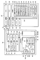
- FIG. 1 shows an information processing apparatus 10 according to the present embodiment.
- the information processing apparatus 10 includes a data management unit 12, an evaluation unit 14, and a command operation unit 22.
- the evaluation unit 14 includes a time management unit 16, an error collection unit 18, and an error analysis unit 20.
- the information processing apparatus 10 is connected to an evaluated unit 24 that is a computer system.
- the evaluated unit 24 performs various processes by each of a plurality of processing units as a computer system.
- the evaluated unit 24 includes a plurality of processing units 26 and a data control unit 28.
- Each of the plurality of processing units 26 is connected to the data control unit 28 via a bus 27 such as a PCI (Peripheral-Component-Interconnect) bus.
- Each of the plurality of processing units 26 includes a storage unit 30 including a first storage unit 32 and a second storage unit 34, a switching unit 36, a control unit 38, and a calculation unit 40.
- symbols A to N are added after the reference numerals to distinguish the processing units 26 or elements from each other. May be handled.
- the information processing apparatus 10 is an example of an information processing apparatus in the disclosed technology
- any one of the plurality of processing units 26 is an example of a processing unit in the disclosed technology.
- the data management unit 12 manages data related to firmware update and evaluation.
- the data management unit 12 stores firmware data for updating firmware and test data for evaluating firmware.
- the data management unit 12 stores the number of firmware to be evaluated and parameters for each firmware evaluation, and can provide information on firmware data, test data, the number of firmware, and parameters for each firmware evaluation.
- the error collection unit 18 collects error information generated during firmware evaluation.
- the error collection unit 18 has a function of displaying the collected error information on a display device or the like.
- the command operation unit 22 outputs a command signal for operating the evaluated unit 24 to the evaluated unit 24.
- command signals include a signal indicating power-on to activate the device (Power_on signal), a signal indicating restart to enable firmware update (Reset signal), and a power-off to stop the operation of the device Signal (Shutdown signal).
- the command operation unit 22 outputs a command signal to the data control unit 28 of the evaluated unit 24.
- the error analysis unit 20 monitors errors that occur in the processing unit 26. For example, the error analysis unit 20 monitors the number and frequency of error occurrences based on information from the error collection unit 18 and the time management unit 16. Further, the error analysis unit 20 may request that the command operation unit 22 output a signal indicating a restart (Reset signal) or a power shutdown signal (Shutdown signal) depending on the result of error monitoring.
- a restart Reset signal
- a power shutdown signal Shut signal
- the data control unit 28 of the evaluated unit 24 controls each of the plurality of processing units 26 based on data and commands from the information processing apparatus 10.
- Each of the plurality of processing units 26 is configured so that the arithmetic unit 40 including a CPU or the like is basically used for hardware resources by firmware stored in the storage unit 30 including the first storage unit 32 and the second storage unit 34 such as a flash memory. Control.
- the control unit 38 outputs various control signals and switches the switching unit 36.
- the switching unit 36 receives the control signal from the control unit 38 and connects the first storage unit 32 and the calculation unit 40 in order to evaluate the firmware stored in the first storage unit 32. Further, the switching unit 36 performs switching so as to connect the second storage unit 34 and the control unit 38 in order to store the data from the control unit 38 in the second storage unit 34.
- the data management unit 12 of the information processing apparatus 10 outputs the first firmware data to the data control unit 28 in order to store the first firmware data of the firmware in the first storage unit 32.
- the data control unit 28 outputs a signal for switching the switching unit 36 in order to store the first firmware data in the first storage unit 32.
- the data management unit 12 of the information processing apparatus 10 indicates a restart to the instruction operation unit 22 so that the plurality of processing units 26 are restarted. Request to output a signal.
- the command operation unit 22 receives a request from the data management unit 12 and outputs a signal indicating restart to the data control unit 28.
- the data control unit 28 receives the signal indicating the restart (Reset signal), resets the switching unit 36, and switches the connection.
- processing by the firmware of the first firmware data is executed by the arithmetic unit 40.
- the data control unit 28 performs error detection.
- the error collection unit 18 of the information processing apparatus 10 collects errors detected by the data control unit 28 as information.
- the data management unit 12 of the information processing apparatus 10 stores the second firmware data in order to store the second firmware data of the firmware in the second storage unit 34.
- the data is output to the data control unit 28.
- the data control unit 28 stores the second firmware data in the second storage unit 34. In this way, by performing firmware update and evaluation in parallel, a plurality of firmware can be evaluated in a short time.
- the information processing apparatus 10 can be realized by, for example, the computer 42 shown in FIG.
- the computer 42 includes a CPU 44, a memory 46, a nonvolatile storage unit 48, an input / output port (I / O) 61, a display 62, a keyboard 63, a mouse 64, and a timer 65.
- the CPU 44, the memory 46, the nonvolatile storage unit 48, the input / output port (I / O) 61, the display 62, the keyboard 63, the mouse 64, and the timer 65 are connected to each other via the bus 60.
- the storage unit 48 can be realized by an HDD (Hard Disk Drive), a flash memory, or the like.
- the storage unit 48 serving as a recording medium stores a test program 50 for causing the computer 42 to function as the information processing apparatus 10. Further, the storage unit 48 stores a web browser (WebBrowser) program 56, a farm data DB 57, a test data DB 58, and an evaluation parameter DB 59, respectively.
- the CPU 44 reads out the web browser program 56 from the storage unit 48, expands it in the memory 46, and executes processing by the web browser program 56. Further, the CPU 44 reads the test program 50 from the storage unit 48 and develops it in the memory 46, and sequentially executes the processes included in the test program 50.
- WebBrowser WebBrowser
- the test program 50 includes a data management process 51, a time management process 52, an error collection process 53, an error analysis process 54, and an instruction operation process 55.
- the CPU 44 operates as the data management unit 12 illustrated in FIG. 1 by executing the data management process 51. That is, the information processing apparatus 10 is realized by the computer 42, and the computer 42 operates as the data management unit 12 illustrated in FIG. 1 by executing the data management process 51.
- the CPU 44 operates as the time management unit 16 illustrated in FIG. 1 by executing the time management process 52.
- a partial area of the memory 46 is used as an area for storing time information obtained by processing of the time management unit 16.
- the CPU 44 operates as the error collection unit 18 shown in FIG. 1 by executing the error collection process 53.
- a partial area of the memory 46 is used as an area for storing error information obtained by the process of the error collection unit 18.
- the CPU 44 operates as the error analysis unit 20 shown in FIG. 1 by executing the error analysis process 54.
- a partial area of the memory 46 is used as an area for storing information indicating an analysis result obtained by the process of the error analysis unit 20.
- the CPU 44 operates as the command operation unit 22 shown in FIG. 1 by executing the command operation process 55.
- the computer 42 that has executed the test program 50 functions as the information processing apparatus 10.
- the storage unit 48 of the computer 42 stores an evaluation parameter DB 59.
- the evaluation parameter DB 59 stores, as one or a plurality of evaluation parameters, information that defines which firmware is to be evaluated with which test data when evaluating the firmware.
- the evaluation parameter includes information that associates firmware data of firmware to be evaluated, test data for evaluating the firmware to be evaluated, and travel time. The travel time is the time for which the CPU is operated by test data for the firmware to be evaluated.
- the evaluation parameter can include the number of errors and the type of error that occur due to the CPU operation by the firmware. When the number of errors and the error type are included in the evaluation parameter, it is preferable that a process to be transferred next is determined by the evaluation parameter corresponding to the number of errors and the error type.
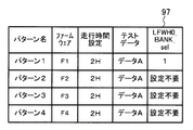
- FIG. 4 shows a first table 97 that is a part of an evaluation plan table that stores, as information, evaluation parameters indicating evaluation contents for evaluating a plurality of firmware.
- FIG. 5 is a diagram of an evaluation plan table that stores, as information, criteria for determining the status transition of firmware evaluation based on errors depending on the type and frequency of errors occurring in the system when systematically evaluating a plurality of firmwares.
- the 2nd table 98 which is a part is shown.
- Fig. 4 shows an example when four types of firmware are systematically evaluated. That is, a table in which the pattern name, firmware, travel time setting, test data, and LFWH (Local Firmware Hub) 0_BANK_sel are associated with each other and are arranged in the order of the evaluation plan can be employed.
- the pattern name is a name for identifying an evaluation parameter group in which firmware, travel time setting, test data, and LFWH0_BANK_sel information are associated with each other.
- the information of the item LFWH0_BANK_sel stores the value of information for switching the bus switch included in the system board whose details will be described later. For example, when the pattern name is “pattern 1” in the first table 97 shown in FIG.
- the firmware evaluation is executed in the order of the pattern 1.2.3.4.
- FIG. 5 shows an example of criteria for determining the status transition of firmware evaluation according to the type and frequency of errors that occur during firmware evaluation.
- FIG. 5 shows an example in which three types of information, ie, CE (Correctable Error), UE (Uncorrectable Error), and FE (Fetal Error), which are information indicating error contents, are used with the error type as the error type item. Show.
- the information CE indicating the error content is, for example, a 1-bit error indicated by the CPU or processor.
- the information UE indicating the error content is, for example, a 2-bit error indicated by the CPU or the processor.
- the information FE indicating the error content is a fatal error such as an internal error or a bus error indicated by the CPU or processor.
- Information in which the frequency of error notification is associated with information CE, UE, and FE indicating error contents is assigned.
- the information UE indicating the error content is “evaluation continuation” when the UE occurs once, “Shutdown” when the UE occurs twice in one minute, “firmware” when the UE occurs twice in 10 minutes, for example.
- Information indicating “switching” is given. That is, information indicating the criteria for determining the state transition of firmware evaluation that the firmware evaluation is continued when the UE occurs once during the running time is the content of the error that occurs during the firmware evaluation.
- test program 50 is an example of an information processing program in the disclosed technology. That is, the test program 50 is an example of an information processing program for causing the computer 42 to function as the information processing apparatus 10.
- the evaluated unit 24 can be realized by, for example, the computer system 70 shown in FIG.
- the computer system 70 includes a plurality of system boards (hereinafter referred to as SB) 84 and a system control board 72.
- SB system boards
- the system can function as a system called a domain having a configuration in which a plurality of SBs 84 are regarded as a functional unit that performs processing combined by a plurality of SBs 84.
- the symbols A to N are added to the symbols and described.
- Each of the plurality of SBs 84 included in the computer system 70 includes a system management controller (Baseboard Management Controller, hereinafter referred to as BMC) 86 and a CPU 90.
- BMC System Management Controller
- Each of the plurality of SBs 84 includes a bus switch (Bus-Exchange) 92 and a local flash memory 94.
- the local flash memory 94 is expressed as LFWH0.
- the local flash memory 94 is a memory for storing firmware, and includes a first memory 95 and a second memory 96 in the present embodiment.
- the first memory 95 is expressed as LFWH0_A.
- the second memory 96 is denoted as LFWH0_B.
- the system control board 72 of the computer system 70 corresponds to the data control unit 28 shown in FIG.
- the SB 84 included in the computer system 70 corresponds to the processing unit 26 shown in FIG.
- the BMC 86 of the SB 84 corresponds to the control unit 38 shown in FIG.
- the CPU 90 corresponds to the calculation unit 40 shown in FIG.
- the bus switch 92 corresponds to the switching unit 36 shown in FIG.
- the local flash memory 94 corresponds to the storage unit 30 shown in FIG.
- the first memory 95 corresponds to the first storage unit 32 shown in FIG. 1, and the second memory 96 corresponds to the second storage unit 34 shown in FIG.
- the SB 84 includes one CPU 90
- the number of CPUs is not limited to one and may be two or more.
- the local flash memory 94 will be described as a local flash memory 94 having two storage areas in which different firmware can be stored in the first memory 95 and the second memory 96.
- the storage area in which the firmware can be stored in the local flash memory 94 is not limited to two, and may be three or more.
- a CPU 90 is connected to the BMC 86 via a serial parallel interface bus (hereinafter referred to as SPI_BUS) 89.
- a bus switch 92 is connected to the BMC 86 via a serial parallel interface bus (hereinafter referred to as SPI bus) 88 and a serial bus 87.
- SPI bus serial parallel interface bus
- I2C bus Inter-Integrated Circuit Bus
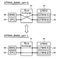
- the bus switch 92 is connected to the local flash memory 94 and switches the connection between the BMC 86 and the CPU 90 and the first memory 95 and the second memory 96 of the local flash memory 94 by a control signal from the serial bus 87.
- the bus switch 92 has a function of switching between the first switching state and the second switching state.
- the first switching state is a state in which the BMC 86 is connected to the first memory 95 via the SPI bus 88 and the CPU 90 and the second memory 96 are connected.
- the second switching state is a state in which the BMC 86 is connected to the second memory 96 via the SPI bus 88 and the CPU 90 and the first memory 95 are connected.
- the BMC 86 also includes a memory BMC_M such as an EEPROM (Electrically-Erasable-Programmable-Read-Only Memory).
- the memory BMC_M stores information indicating whether firmware can be updated (hereinafter referred to as information LFWH0_update), and information for switching the bus switch 92 (hereinafter referred to as information LFWH0_BANK_sel). For example, as an example of the value of the information LFWH0_update, “1” is stored when the firmware is updated, and “0” is stored when the firmware update is prohibited.
- the information LFWH0_BANK_sel is information for setting the connection destination of the CPU 90 and the BMC 86 and the first memory 95 and the second memory 96.
- the system control board 72 included in the computer system 70 includes a CPU 78, a memory 79, a nonvolatile storage unit 74, an input / output port (I / O) 77, and a bus interface (I / F) 80 such as a PCI bus.
- the CPU 78, the memory 79, the nonvolatile storage unit 74, the input / output port (I / O) 77, and the bus interface (I / F) 80 are connected to each other via a bus 81.
- the storage unit 74 stores a control program 75 and a web user interface program 76. In FIG. 2, the web user interface program 76 is represented as WebUI_PG.
- the CPU 78 reads out the control program 75 and the web user interface program 76 from the storage unit 74, loads them into the memory 79, and executes processing by the control program 75 and the web user interface program 76.
- the bus interface 80 of the system control board 72 is connected to each of the BMCs 86 of the plurality of SBs 84 via the PCI bus 82. Further, the input / output port 77 is connected to the input / output port 61 via a LAN (Local Area Network) 68, so that the computer 42 and the computer system 70 are connected so as to be able to exchange information.
- the system control board 72 operates as the data control unit 28 shown in FIG. 1 when the CPU 78 executes the control program 75 and the web user interface program 76.
- firmware update and evaluation are performed in parallel using the first memory 95 (LFWH0_A) and the second memory 96 (LFWH0_B) for storing the firmware of the SB84.
- a test for quality assurance is performed, but a hardware or firmware failure occurs, the firmware is recreated each time, and a long evaluation time is required.
- a plurality of firmware may be prepared and the optimum firmware may be determined based on the evaluation result.
- firmware update and firmware evaluation are executed alternately (serially), the time required for processing increases according to the number of firmware to be updated and evaluated. Therefore, in this embodiment, a plurality of storage areas for storing firmware are prepared, and firmware update and evaluation are performed in parallel, thereby reducing the time required for firmware evaluation.
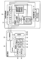
- FIG. 6 shows the relationship between the units included in the information processing apparatus 10 and the relationship between the units included in the evaluated unit 24.
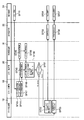
- FIG. 7 shows a flow of processing related to each unit of the information processing apparatus 10 as a sequential flow.
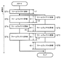
- FIG. 8 is a diagram for explaining that the time can be shortened by updating and evaluating a plurality of firmwares.
- FIG. 9 shows a flow of processing related to each unit of the information processing apparatus 10 when an error occurs in the evaluated unit 24 as a sequential flow.
- the firmware data and test data of the firmware to be evaluated are stored in the data management unit 12.
- the data management unit 12 transmits firmware data and test data of the firmware to be evaluated to the processing unit 26 installed in the evaluated unit 24 (see also FIG. 6).
- the data management unit 12 instructs the command operation unit 22 to perform a restart instruction for restart (Reset) for enabling the firmware, or power shutdown (Shutdown) for stopping the operation of the device when all the firmware evaluations are completed.
- a power-off instruction is output (see also FIG. 6).
- the data management unit 12 instructs the command operation unit 22 to turn on the information processing apparatus 10 in order to cause the evaluated unit 24 (at least the processing unit 26) to turn on the power (see FIG. 7 step SF01).
- the command operating unit 22 commands the evaluated unit 24 to turn on the power in response to an instruction from the data management unit 12 (step SF02).
- the evaluated unit 24 receives the command from the command operating unit 22 and executes power-on (step SF03). In other words, the evaluated unit 24 executes a process in which the data control unit 28 of the evaluated unit 24 receives a command from the command operating unit 22 and powers on the entire apparatus including at least the processing unit 26.
- the data management unit 12 transmits information indicating whether the first firmware update is performed in the first storage unit 32 or the second storage unit 34.
- the data management unit 12 transmits the LFWH0_BANK_sel signal (here, a signal of value “1”) based on the information of LFWH0_BANK_sel in the first table 97 to the evaluated unit 24 based on the information in the evaluation plan table (step S40).
- the data control unit 28 of the evaluated unit 24 receives the LFWH0_BANK_sel signal transmitted from the data management unit 12, and switches the switching unit 36 of the processing unit 26 (step SF05).
- the processing unit 26 of the evaluated unit 24 executes processing up to the state for updating the firmware (step SF06).
- the process of step SF06 is a process of starting up until the operating system is activated.
- the data management unit 12 transmits the value “1” of the information LFWH0_update to the evaluated unit 24 so that the processing unit 26 can update the firmware (step SF07).
- the to-be-evaluated part 24 performs the process which makes the firmware update possible in the process part 26 (step SF08). That is, in the evaluated unit 24, the data control unit 28 receives information LFWH0_update from the data management unit 12. Then, the data control unit 28 sets the value “1” of the information LFWH0_update in the control unit 38, so that the firmware data can be written into the first storage unit 32 of the processing unit 26.
- the data management unit 12 transmits the firmware data of the first firmware to the evaluated unit 24 (step SF09).
- the evaluated unit 24 After receiving firmware firmware data from the data management unit 12, the evaluated unit 24 updates the firmware (step SF10).
- the data control unit 28 receives the firmware data of the first firmware and writes the firmware data to the first storage unit 32 via the control unit 38.
- the data control unit 28 notifies the data management unit 12 that the firmware update is completed (step SF11).
- the data management unit 12 sets the value “0” of the information LFWH0_update to be in a state in which the firmware cannot be updated after the first firmware update is completed in the processing unit 26 when the first firmware update is completed. It transmits to the to-be-evaluated part 24 (step SF12).
- the to-be-evaluated part 24 performs the process which makes the firmware update impossible in the process part 26 (step SF13). Further, the data management unit 12 instructs the instruction operation unit 22 to restart the processing unit 26 of the evaluated unit 24 in order to validate the updated first firmware (step SF14).
- the command operation unit 22 receives an instruction from the data management unit 12, and transmits a restart command to the evaluated unit 24 (step SF15).
- the evaluated unit 24 (data control unit 28) receives the restart command from the command operating unit 22, and restarts the processing unit 26 (step SF16).
- the state of the bus switch 92 is switched by restarting the processing unit 26 of the evaluated unit 24 (see also FIG. 3). In other words, it becomes possible for the computing unit 40 to operate with firmware based on the firmware data written in the first storage unit 32, that is, the computing unit 40 can execute the firmware data.
- the processing unit 26 is restarted to execute processing up to the state for performing the firmware evaluation (OS_boot: processing to start up until the operating system is activated (step SF17)).
- OS_boot processing to start up until the operating system is activated
- the data management unit 12 transmits the test data to the data control unit 28 of the evaluated unit 24 (step SF18).
- the test data received by the data control unit 28 from the data management unit 12 is transmitted to the calculation unit 40 via the control unit 38.
- the calculation unit 40 performs firmware evaluation using the test data from the data management unit 12 (step SF19).
- the data management unit 12 transmits information indicating that the firmware evaluation has started to the time management unit 16 (step SF20).
- the time management unit 16 receives the information from the data management unit 12 and records the evaluation start time (step SF21).
- the time management unit 16 transmits the recorded evaluation start time to the error analysis unit 20 (step SF22).
- the error analysis unit 20 acquires the evaluation start time (step SF23), and starts analysis for error analysis. For example, measurement of travel time is started.
- the data management unit 12 determines whether or not there is unevaluated firmware (step SF24). When there is unevaluated firmware, the data management unit 12 proceeds to a process for updating the next firmware. That is, the data management unit 12 transmits the value “1” of the information LFWH0_update to the evaluated unit 24 so that the processing unit 26 can update the next firmware (step SF25). The evaluated unit 24 executes processing for making the next firmware updateable in the processing unit 26 (step SF26). Further, the data management unit 12 transmits the firmware data of the next firmware to the evaluated unit 24 (step SF27). The evaluated unit 24 receives the firmware data transmitted by the data management unit 12, and executes the next firmware update (step SF10). That is, in the evaluated unit 24, the data control unit 28 receives the firmware data of the next firmware, and writes the firmware data to the second storage unit 34 via the control unit 38.
- the data control unit 28 When the next firmware update is completed in the processing unit 26, the data control unit 28 notifies the data management unit 12 that the next firmware update is completed (step SF29).
- the data management unit 12 transmits the value “0” of the information LFWH0_update to the evaluated unit 24 so that the processing unit 26 cannot update the firmware when the next firmware update is completed ( Step SF30).
- the to-be-evaluated part 24 performs the process which makes the update of a firmware impossible in the process part 26 (step SF31).
- the data management unit 12 transmits the travel time set in the first table 97 to the time management unit 16 for the first firmware evaluation (step SF32).
- the time management unit 16 receives the travel time from the data management unit 12 (step SF33), performs time management (monitoring) until the received travel time elapses, and passes the travel time to the data management unit 12 when the travel time elapses. Notification is made (step SF34).
- the data management unit 12 receives the notification of the elapsed travel time from the time management unit 16 and considers that the end of the evaluation has been notified (step SF37).
- the data management unit 12 transmits an evaluation parameter related to the firmware evaluation to the error analysis unit 20 (step SF35).
- the error analysis unit 20 acquires the evaluation parameter transmitted from the data management unit 12 (step SF36), and uses the evaluation parameter for error analysis.
- the data management unit 12 instructs the command operation unit 22 to stop the operation of the processing unit 26 when there is no unevaluated firmware and all the evaluations are completed (step SF38).
- the command operation unit 22 receives an instruction from the data management unit 12, and transmits a power-off command to the evaluated unit 24 (step SF39).
- the evaluated unit 24 receives the power-off command from the command operating unit 22, and shuts off the power of the evaluated unit 24 (step SF40).
- the data management unit 12 may wait for the evaluation to end.
- step SF37 If there is unevaluated firmware after step SF37, the process returns to step SF14 and the above processing is repeated.
- the information processing apparatus 10 can perform update and evaluation in parallel for a plurality of firmware, and can shorten the time for evaluating the plurality of firmware. That is, when the evaluation plan according to the first table 97 shown in FIG. 4 is executed, first, as shown in FIG. ) Is updated (step ST1).
- the firmware (F1) is updated to the first storage unit 32 of the processing unit 26.
- the information processing apparatus 10 executes the evaluation of the firmware (F1) (step ST2), and executes the update of the firmware (F2) by the pattern 2 in parallel with the process of step ST2 (step ST3).
- the firmware (F2) is updated to the second storage unit 34 of the processing unit 26. Since the information processing apparatus 10 uses the first storage unit 32 and the second storage unit 34 included in the first storage unit 32 to update and evaluate the firmware, the firmware (F1) evaluation and the firmware ( Wait until both processes of F2) are completed.
- the information processing apparatus 10 executes the update of the firmware (F3) by the pattern 3 to the evaluated unit 24 (step ST4). ).
- the firmware (F3) is updated to the first storage unit 32 of the processing unit 26.
- the information processing apparatus 10 executes the evaluation of the firmware (F2) (step ST5).
- the second storage unit 34 of the processing unit 26 is used. The information processing apparatus 10 waits until both processing of firmware (F2) evaluation and firmware (F3) update is completed.
- the information processing apparatus 10 executes the firmware (F3) evaluation (step ST6).
- the firmware (F4) is updated by the pattern 4 (step ST7).
- the firmware (F4) is updated to the second storage unit 34 of the processing unit 26.
- the information processing apparatus 10 waits until both processing of firmware (F3) evaluation and firmware (F4) update is completed.
- the information processing apparatus 10 executes the firmware (F4) evaluation (step ST8) and ends the evaluation of all the firmware.
- processing of firmware (F1) evaluation (step ST2) and firmware (F2) update (step ST3) are performed in parallel. Therefore, both processes are completed in the longer time (time t2) of the time required for the evaluation of the firmware (F1) and the time required for updating the firmware (F2). Further, the processes of the firmware (F2) evaluation (step ST5) and the firmware (F3) update (step ST4) are performed in parallel. For this reason, both processes are completed in the longer time (time t4) of the time required for the firmware (F2) evaluation and the time required for the firmware (F3) update. Further, the processes of the firmware (F3) evaluation (step ST6) and the firmware (F4) update (step ST7) are performed in parallel. For this reason, both processes are completed in the longer time (time t6) of the time required for the evaluation of the firmware (F3) and the time required for the update of the firmware (F4).
- the sum of the time required for the evaluation of the four different firmwares is the sum of the longer time in each parallel processing (t1 + t2 + t4 + t6 + t8 in the example of FIG. 8), and when the firmware update and evaluation processes are repeated alternately. It can be shortened in comparison.
- the evaluated unit 24 transmits error information to the error collecting unit 18 (step SF41).
- the error collecting unit 18 receives error information from the evaluated unit 24 (step SF43), and notifies the time management unit 16 of information indicating that an error has occurred in the evaluated unit 24 (step SF44).
- the time management unit 16 records the timing at which the notification of error occurrence from the error collection unit 18 is received (triggered) as the error occurrence time (step SF45).
- the time management unit 16 transmits the recorded error occurrence time to the error analysis unit 20 (step SF46).
- the error analysis unit 20 acquires the error occurrence time transmitted from the time management unit 16 (step SF49).
- the error collection unit 18 transmits information indicating the content of the generated error to the error analysis unit 20 together with the notification of the occurrence of the error (step SF47).
- the error analysis unit 20 identifies information indicating the content of the error transmitted from the error collection unit 18 (step SF48).
- the error analysis unit 20 performs analysis on the error using the identified error content and the acquired error occurrence time (step SF50). Analysis for errors is performed using the number of errors, the frequency of occurrence of errors, and evaluation parameters.
- the data management unit 12 sets the processing unit 26 of the evaluated unit 24 at the timing when the firmware update processing being executed in parallel ends.
- Restart That is, the data management unit 12 instructs the command operation unit 22 to give a command to restart the processing unit 26 (step SF52).
- the command operation unit 22 receives an instruction from the data management unit 12, and transmits a restart command to the evaluated unit 24 (step SF53).
- the evaluated unit 24 (data control unit 28) receives the restart command from the command operating unit 22, and restarts the processing unit 26 (step SF54).
- the data management unit 12 issues an instruction to immediately stop the operation of the processing unit 26 of the evaluated unit 24 (Shutdown).
- the operation unit 22 is instructed (step SF55).
- the command operation unit 22 receives an instruction from the data management unit 12, and transmits a power-off command to the evaluated unit 24 (step SF56).
- the evaluated unit 24 receives the power-off command from the command operation unit 22, and shuts off the power of the evaluated unit 24 to stop at least the operation of the processing unit 26 (step SF57).
- SB84A SB84A
- the CPU 44 of the computer 42 executes each process included in the test program 50 stored in the storage unit 48. That is, the CPU 44 of the computer 42 expands the data management process 51, time management process 52, error collection process 53, error analysis process 54, and command operation process 55 stored in the test program 50 of the storage unit 48 in the memory 46. Execute. As a result, the processing routines shown in FIGS. 10 to 16 are executed.
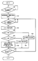
- FIG. 10 is a flowchart showing the flow of processing in the data management unit 12.
- the information processing apparatus 10 is realized by the computer 42, and the computer 42 operates as the data management unit 12 (FIG. 1) by developing the data management process 51 in the memory 46 and executing it by the CPU 44.
- the firmware data of the firmware to be evaluated is stored in the firmware data DB 57, and the test data is stored in the test data DB 58.
- step 100 in order to turn on the computer system 70, the instruction operation process 55 (instruction operation unit 22) is instructed to turn on the computer system 70.
- step 102 based on the information in the evaluation plan table, the value based on the information of LFWH0_BANK_sel in the first table 97 (here, the value “1”) is transmitted to the computer system 70 as the LFWH0_BANK_sel signal.
- step 104 the computer system 70 waits until the firmware can be updated, and the process proceeds to step 106.
- the system control board 72 receives the LFWH0_BANK_sel signal via the input / output port 77, and the bus switch 92 of the SB 84 is switched.
- the SB 84 of the computer system 70 executes a process (OS_boot: process for starting up the operating system) up to a state where the firmware can be updated.
- OS_boot process for starting up the operating system
- the first memory 95 and the second memory 96 of the local flash memory 94 are alternately connected by setting and resetting the bus switch 92 as will be described later, so that information on LFWH0_BANK_sel There is no need to set the value by.
- the value “1” of the information LFWH0_update is transmitted to the computer system 70 so that the firmware can be updated in SB84.
- the system control board 72 receives the value of the information LFWH0_update and sets it in the BMC 86 of the SB84. When the value of the information LFWH0_update is set in the BMC 86, the first memory 95 of the SB 84 becomes ready to write firmware data.
- the firmware data of the first firmware is transmitted to the computer system 70. When the firmware data of the first firmware is transmitted, the update of the first firmware is started in SB84.
- the system control board 72 receives the first firmware firmware data and writes the first firmware data to the first memory 95 via the BMC 86.
- step 110 the firmware is updated.
- step 114 the storage of data in the local flash memory 94 is prohibited (the firmware cannot be updated) with the end of the first firmware update, so that the value “0” of the information LFWH0_update is set to the computer system 70.
- the system control board 72 receives the value of the information LFWH0_update and sets it in the BMC 86 of the SB84. As a result, the first memory 95 of the SB 84 becomes unable to write firmware data.
- next step 116 in order to validate the updated first firmware, an instruction to the instruction operation process 55 (instruction operation unit 22) is executed so that an instruction to restart (reset) the SB 84 of the computer system 70 is executed. .
- the command operation process 55 receives an instruction from the data management process 51 and transmits a restart command to the computer system 70.
- the process waits until the computer system 70 can evaluate the firmware, that is, until the OS is in the operating state in SB 84, and proceeds to step 120.
- next step 122 it is determined whether there is unevaluated firmware. This determination can be made from the total number of firmware data registered in the data management process 51. If the determination in step 122 is affirmative, the process proceeds to step 124, and the value “1” of the information LFWH0_update is transmitted to the computer system 70 so that the next firmware can be updated. In the next step 126, update of the next firmware is started by transmitting the firmware data of the next firmware.
- step 130 transmission of the firmware data of the firmware is continued (until affirmative determination is made in step 130) until transmission to the computer system 70 is completed (step 128), and firmware update is executed.
- step 130 an affirmative determination is made in step 130 and the firmware update is released in step 132. That is, in step 132, the value “0” of the information LFWH0_update is transmitted to the computer system 70.
- step 134 negative determination is repeated until the evaluation of the firmware under evaluation is completed. If the determination in step 134 is affirmative, the process proceeds to step 136, and it is determined whether or not the evaluation of all the firmware set in the first table 97 has been completed. When all the firmware evaluations have been completed, an affirmative determination is made at step 136 and the process proceeds to step 138 to instruct the instruction operation process 55 (instruction operation unit 22) to give an instruction to stop the operation of the computer system 70. As will be described later, the command operation process 55 transmits a power-off command to the computer system 70 to shut down the computer system 70. On the other hand, if the determination in step 136 is negative, there is firmware that has not been evaluated, so the process returns to step 116 and the above process is repeated.
- FIG. 11 is a flowchart showing the flow of processing in the error collection process 53.
- the information processing apparatus 10 is realized by the computer 42, and the error collection process 53 is expanded in the memory 46 and executed by the CPU 44, whereby the computer 42 operates as the error collection unit 18 (FIG. 1).
- the error collection process 53 acquires error information from the system control board 72 when an error occurs during the evaluation of the firmware, transmits the error content to the error analysis process 54 (error analysis unit 20), and that an error has occurred. Is transmitted to the time management process 52 (time management unit 16).
- step 140 the process waits until a notification indicating that the firmware evaluation has started is started.
- the process proceeds to step 141.
- step 141 the presence / absence of an error in SB84 is detected, and in step 142, it is determined whether an error has occurred in SB84. That is, whether or not an error has occurred in the system control board 72 is detected by polling processing (polling) at step SB84.
- the information processing apparatus 10 is realized by the computer 42, and the computer 42 operates as the error analysis unit 20 (FIG. 1) when the error analysis process 54 is expanded in the memory 46 and executed by the CPU 44.
- the error process 54 performs error analysis processing using the error information transmitted from the error collection process 53 (error collection unit 18). That is, the error analysis process 54 performs processing on error contents (CE, UE, FE) from the error information, the firmware evaluation start time acquired from the time management process 52 (time management unit 16), and the time when the error occurred. Do.
- step 150 the process waits until a notification indicating that the evaluation of the firmware has started is started.
- the process proceeds to step 152.
- step 152 the start time of firmware evaluation is acquired from the time management process 52 (time management unit 16).
- step 154 negative determination is repeated until error information is received from the error collection process 53 (error collection unit 18).
- Step 156 it is identified whether the error content is CE, UE, or FE.
- Step 158 it is determined whether or not the content of the error is CE. If the determination in step 158 is affirmative, the process proceeds to step 168 after executing the process of step 160.
- step 162 determines whether or not the content of the error is UE. If the determination in step 162 is affirmative, the process proceeds to step 168 after executing the process of step 164.
- step 166 transmits a power shutdown command to the computer system 70 to the command operation process 55 (command operation unit 22). 70 is turned off. Note that in step 166, it may be instructed to transmit information requesting the power-off of the computer system 70 to the data management process 51 (data management unit 12). In this case, it is possible to instruct the power management command to be transmitted from the data management process 51 (data management unit 12) to the command operation process 55 (command operation unit 22).
- step 168 it is determined whether or not the firmware evaluation is completed. Step 168 is unconditionally affirmed when step 166 is passed. When the process passes through step 160, a determination is made on the result of the process described later in step 160. Similarly, when the process goes through step 164, a determination corresponding to the result of the process described later in step 164 is made. If an affirmative determination is made in step 168, this processing routine is terminated. If a negative determination is made, the process returns to step 154. If a firmware evaluation end notification is made between steps 152 to 166, the processing routine can be ended assuming that an affirmative determination is made in step 168 as an interrupt process.
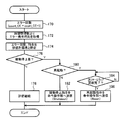
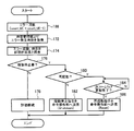
- step 160 of FIG. 12 when the error content is CE, the processing routine shown in FIG. 13 is executed.
- step 172 the current time is acquired from the time management process 52 (time management unit 16), and the error occurrence time is acquired every time an error occurs.
- step 174 the error occurrence time interval obtained in step 172 is obtained, and the error frequency obtained in step 170 and the error occurrence frequency according to the obtained error occurrence time interval are collated with the evaluation plan table. That is, it collates with each information of the error type “CE” in the second table 98.
- step 176 it is determined whether or not the computer system 70 needs to be stopped using the collation result in step 174. If a negative determination is made in step 176, information indicating that the firmware evaluation is continued is set in step 178, and this routine is terminated. Information indicating that the firmware evaluation is continued is used for the determination in step 168 of FIG.
- step 176 when an affirmative determination is made in step 176, the process proceeds to step 180, and it is determined whether or not the collation result in step 174 is information indicating restart.
- step 180 an instruction to cut off the power supply of the computer system 70 is transmitted to the command operation process 55 (command operation unit 22), and the power supply of the computer system 70 is cut off.
- step 166 information for requesting power-off of the computer system 70 may be transmitted to the data management process 51 (data management unit 12). In this case, a power-off instruction can be transmitted from the data management process 51 (data management unit 12) to the command operation process 55 (command operation unit 22).
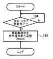
- step 180 If the determination in step 180 is affirmative, the process waits until the next firmware update is completed (negative determination is repeated in step 184). When the update of the next firmware is completed (when an affirmative determination is made in step 184), the process proceeds to step 186, and an instruction to restart the SB 84 of the computer system 70 is transmitted to the instruction operation process 55 (instruction operation unit 22). Then, the SB 84 of the computer system 70 is restarted.
- step 186 information for requesting restart of the SB 84 of the computer system 70 may be transmitted to the data management process 51 (data management unit 12). In this case, a restart instruction can be transmitted from the data management process 51 (data management unit 12) to the command operation process 55 (command operation unit 22).
- step 164 of FIG. 12 when the error content is UE, the processing routine shown in FIG. 14 is executed.
- the process in FIG. 14 is almost the same as the process in FIG.
- the difference between the process of FIG. 14 and the process of FIG. 13 is that the error content is “CE” or the error content is “UE”.
- step 188 in FIG. 14 the error content can be realized by replacing “CE” with “UE”.
- FIG. 15 is a flowchart showing the flow of processing in the time management process 52.
- the computer 42 operates as the time management unit 16 (FIG. 1).
- the time management process 52 records the firmware evaluation start time and error occurrence time, acquires the firmware evaluation time from the data management process 51 (data management unit 12), and determines the error occurrence time as the error analysis process 54 ( To the error analyzer 20).
- step 200 the process waits until a notification indicating that the evaluation of the firmware has started is started.
- the process proceeds to step 202.
- step 202 the firmware evaluation start time is recorded.
- the start time can be obtained by referring to the timer 65 and acquiring the current time.
- step 212 it is determined whether or not the travel time acquired in step 204 has elapsed. If a negative determination is made in step 212, the process returns to step 206. If an affirmative determination is made, the process proceeds to step 214.
- the running time has elapsed, it is a time when the evaluation of the firmware has been completed, and therefore information indicating the end of the evaluation is transmitted to the data management process 51 (data management unit 12) in step 214.
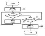
- FIG. 16 is a flowchart showing the flow of processing in the command operation process 55.
- the information processing apparatus 10 is realized by the computer 42, and the instruction operation process 55 is expanded in the memory 46 and executed by the CPU 44, whereby the computer 42 operates as the instruction operation unit 22 (FIG. 1).
- the command operation process 55 can transmit a power-on command for the entire computer system 70 to the computer system 70. Further, in the command operation process 55, a restart command and a shutdown command instructed by the data management process 51 (data management unit 12), the error analysis process 54 (error analysis unit 20) are provided. To the computer system 70.
- step 220 a power-on command for the entire computer system 70 that is instructed by the data management process 51 (data management unit 12) and the error analysis process 54 (error analysis unit 20) is output to the computer system 70.
- the operation of the computer system 70 is started when the computer system 70 receives a power-on command.
- step 222 it is determined whether or not a restart instruction has been issued from the data management process 51 (data management unit 12) or the error analysis process 54 (error analysis unit 20). If the result in step 222 is affirmative, a restart command signal is output to the computer system 70 in step 224, and the process returns to step 222.
- step 226 it is determined in step 226 whether or not a power shutdown instruction has been issued from the data management process 51 (data management unit 12) or the error analysis process 54 (error analysis unit 20). . If the determination in step 226 is negative, the process returns to step 222. If the determination is affirmative, in step 228, a power-off command signal is output to the computer system 70, and this routine is terminated.
- firmware that is different from the firmware under evaluation can be updated.
- firmware evaluation firmware updates that are different from the firmware being evaluated are processed, thereby reducing the time required for firmware evaluation compared to alternating firmware updates and evaluations.
- Can do For example, in the case of evaluating four types of firmware, a case where a processing time of 1 hour is required for firmware update and a processing time of 2 hours is required for firmware evaluation is taken as an example. In the technique of continuously processing each update and evaluation process for each of the four types of firmware, 12 hours are required for the entire evaluation. On the other hand, in this embodiment, since parallel processing is possible, all evaluations can be completed in a processing time of 9 hours.
- the firmware evaluation time due to the occurrence of an error. For example, if it can be determined that the significance of continuing the evaluation process has been lost due to the error type, error occurrence frequency, and error occurrence location, the evaluation is terminated before the set evaluation time (running time) elapses. When the evaluation ends before the set evaluation time elapses, it is possible to perform hardware maintenance by temporarily shutting down the next firmware evaluation or power supply, and the firmware evaluation time can be shortened. become.
- the firmware evaluation time can be shortened.
- FIG. 17 shows, as an example, an evaluation table 99 that explicitly provides a firmware operation result to a user who operates the information processing apparatus 10.
- the evaluation table 99 is obtained by adding, to the first table 97, information in which the number of errors that have occurred, the evaluation start time, and the end time are associated with evaluation parameters.
- the evaluation table 99 can explicitly provide evaluation results of a plurality of firmware to a user who operates the information processing apparatus 10.
- FIG. 18 shows the second table 98 (1).
- the second table 98 (1) is obtained by omitting a criterion relating to the frequency of error occurrence as a criterion for determining the state transition of firmware evaluation. More specifically, the second table 98 (1) is information only when there is an error notification, instead of the frequency of error occurrence in the second table 98, and information indicating error contents (CE, UE, FE) Information indicating the status transition of the firmware evaluation associated with the information).
- CE error contents
- the difference between the second embodiment and the first embodiment is the processing in the error analysis process 54 and the processing in the time management process 52.
- the processing routine of FIG. 19 is executed instead of the processing routine of FIG.
- the processing routine of FIG. 20 is executed instead of the processing routine of FIG.
- the processing routine of FIG. 21 is executed instead of the processing routine of FIG.
- differences will be described.
- step 160 and step 164 of FIG. 12 is processed only by step 161 of FIG. That is, when the content of the error is CE or UE, step 161 is executed.
- FIG. 13 the difference between FIG. 13 and FIG. 20 is that the processing of FIG. 20 processes only the processing of step 184 and step 186 of FIG. That is, when the content of the error is CE or UE, the process waits until the next firmware update is completed (determination is negative in step 184). When the next firmware update is completed (when an affirmative determination is made in step 184), the process proceeds to step 186, and an instruction to restart the SB 84 of the computer system 70 is transmitted to the instruction operation process 55 (instruction operation unit 22). Then, the processing routine of FIG.
- step 212 in FIG. 15 is executed. That is, in the process of FIG. 21, when the determination process of step 206 is negative, the determination of the elapsed travel time at step 212 of FIG. If a negative determination is made in step 211, the process returns to step 206, and if an affirmative determination is made, the process proceeds to step 214. When the process of step 210 is completed, the process proceeds to step 214.
- the evaluation process when an error occurs even once, the evaluation process is terminated to switch to the next firmware evaluation.
- firmware update and evaluation that do not cause an error can be realized. Further, if an error occurs even once, the evaluation is switched to the next firmware evaluation, so that the evaluation time can be further shortened.
- the criterion for the case where there is an error notification is set as the second table 98 which is a part of the evaluation plan table indicating the criterion for determining the state transition of firmware evaluation.
- the second table 98 which is a part of the evaluation plan table indicating the criterion for determining the state transition of firmware evaluation.
- a modified example of the second table 98 will be described as a third embodiment with reference to FIGS. Since the third embodiment has substantially the same configuration as the first and second embodiments, the same parts are denoted by the same reference numerals and detailed description thereof is omitted.
- FIG. 22 shows an example of the second table 98 (2).
- the second table 98 (2) is obtained by adding a criterion when there is no error notification to the second table 98 of FIG. 5 as a criterion for determining the state transition of the firmware evaluation.
- information indicating the status transition of firmware evaluation when there is no error notification is replaced with information (CE, UE, FE) indicating error contents, instead of the frequency of error occurrence. Associating and storing.
- the difference between the third embodiment and the first embodiment is the processing in the time management process 52. Specifically, the processing routine of FIG. 23 is executed instead of the processing routine of FIG. Hereinafter, differences will be described.
- step 204 As processing in the time management process 52, the difference between FIG. 15 and FIG. 23 is that processing related to the occurrence of no error is added to the processing in FIG. That is, in the process of FIG. 23, when the process of step 204 is completed, the process proceeds to step 206 after counting the error-free time in step 230. Further, when a negative determination is made at step 206, it is determined whether or not the error-free state at step 232 has passed one hour. If a negative determination is made in step 232, the process proceeds to step 212, and if an affirmative determination is made, the process proceeds to step 214. When the process of step 210 is completed, the time count when an error has not occurred is reset (set to an initial value, for example, “0”), and then the process proceeds to step 214.
- the firmware to be evaluated is regarded as satisfying a predetermined constant evaluation criterion, and switching to the next firmware evaluation is performed.
- the evaluation process ends.
- the program in the disclosed technology can be provided in a form recorded on a recording medium such as a CD-ROM or a DVD-ROM.
Landscapes
- Engineering & Computer Science (AREA)
- Theoretical Computer Science (AREA)
- Computer Hardware Design (AREA)
- Quality & Reliability (AREA)
- Physics & Mathematics (AREA)
- General Engineering & Computer Science (AREA)
- General Physics & Mathematics (AREA)
- Stored Programmes (AREA)
- Debugging And Monitoring (AREA)
Abstract
L'invention porte sur un dispositif de traitement d'informations dans lequel le temps d'évaluation de micrologiciels est raccourci au niveau d'une face latérale. Une unité de gestion de données (12) stocke un premier micrologiciel dans une première section de stockage (32), au moyen d'une section de contrôle de données (28) et d'une section de commutation (36). De manière à activer le premier micrologiciel, une section de contrôle d'instructions (22) règle une période d'évaluation dans laquelle elle redémarre l'unité de traitement (26), change la connexion de la section de commutation (36) et évalue le premier micrologiciel. Durant cette évaluation, elle stocke un second micrologiciel dans une seconde section de stockage (34). Par mise à jour et évaluation des micrologiciels par réalisation de leur traitement en parallèle, une pluralité de micrologiciels peuvent être évalués en une courte durée.
Priority Applications (2)
| Application Number | Priority Date | Filing Date | Title |
|---|---|---|---|
| JP2014507253A JP6024742B2 (ja) | 2012-03-30 | 2012-03-30 | 情報処理装置、情報処理方法、情報処理プログラム、及び記録媒体 |
| PCT/JP2012/058682 WO2013145292A1 (fr) | 2012-03-30 | 2012-03-30 | Dispositif de traitement d'informations, procédé de traitement d'informations, programme de traitement d'informations et support d'enregistrement |
Applications Claiming Priority (1)
| Application Number | Priority Date | Filing Date | Title |
|---|---|---|---|
| PCT/JP2012/058682 WO2013145292A1 (fr) | 2012-03-30 | 2012-03-30 | Dispositif de traitement d'informations, procédé de traitement d'informations, programme de traitement d'informations et support d'enregistrement |
Publications (1)
| Publication Number | Publication Date |
|---|---|
| WO2013145292A1 true WO2013145292A1 (fr) | 2013-10-03 |
Family
ID=49258655
Family Applications (1)
| Application Number | Title | Priority Date | Filing Date |
|---|---|---|---|
| PCT/JP2012/058682 Ceased WO2013145292A1 (fr) | 2012-03-30 | 2012-03-30 | Dispositif de traitement d'informations, procédé de traitement d'informations, programme de traitement d'informations et support d'enregistrement |
Country Status (2)
| Country | Link |
|---|---|
| JP (1) | JP6024742B2 (fr) |
| WO (1) | WO2013145292A1 (fr) |
Cited By (1)
| Publication number | Priority date | Publication date | Assignee | Title |
|---|---|---|---|---|
| JP2019106042A (ja) * | 2017-12-13 | 2019-06-27 | トヨタ自動車株式会社 | 演算装置 |
Citations (4)
| Publication number | Priority date | Publication date | Assignee | Title |
|---|---|---|---|---|
| JPH05224992A (ja) * | 1992-02-13 | 1993-09-03 | Hitachi Ltd | プログラムテスト装置 |
| JP2002169693A (ja) * | 2000-11-30 | 2002-06-14 | Digital Electronics Corp | 制御用表示装置、および、そのプログラムが記録された記録媒体 |
| JP2003316609A (ja) * | 2002-04-24 | 2003-11-07 | Konica Minolta Holdings Inc | 電子機器、画像形成装置およびその動作監視方法 |
| JP2008165627A (ja) * | 2006-12-28 | 2008-07-17 | Fujitsu Ltd | 組込装置および制御方法 |
Family Cites Families (1)
| Publication number | Priority date | Publication date | Assignee | Title |
|---|---|---|---|---|
| JPH08106381A (ja) * | 1994-10-03 | 1996-04-23 | Fuji Electric Co Ltd | プログラムの評価試験方法 |
-
2012
- 2012-03-30 WO PCT/JP2012/058682 patent/WO2013145292A1/fr not_active Ceased
- 2012-03-30 JP JP2014507253A patent/JP6024742B2/ja not_active Expired - Fee Related
Patent Citations (4)
| Publication number | Priority date | Publication date | Assignee | Title |
|---|---|---|---|---|
| JPH05224992A (ja) * | 1992-02-13 | 1993-09-03 | Hitachi Ltd | プログラムテスト装置 |
| JP2002169693A (ja) * | 2000-11-30 | 2002-06-14 | Digital Electronics Corp | 制御用表示装置、および、そのプログラムが記録された記録媒体 |
| JP2003316609A (ja) * | 2002-04-24 | 2003-11-07 | Konica Minolta Holdings Inc | 電子機器、画像形成装置およびその動作監視方法 |
| JP2008165627A (ja) * | 2006-12-28 | 2008-07-17 | Fujitsu Ltd | 組込装置および制御方法 |
Cited By (1)
| Publication number | Priority date | Publication date | Assignee | Title |
|---|---|---|---|---|
| JP2019106042A (ja) * | 2017-12-13 | 2019-06-27 | トヨタ自動車株式会社 | 演算装置 |
Also Published As
| Publication number | Publication date |
|---|---|
| JPWO2013145292A1 (ja) | 2015-08-03 |
| JP6024742B2 (ja) | 2016-11-16 |
Similar Documents
| Publication | Publication Date | Title |
|---|---|---|
| CN105683919B (zh) | 用于安全关键软件应用的多核处理器故障检测 | |
| US10585755B2 (en) | Electronic apparatus and method for restarting a central processing unit (CPU) in response to detecting an abnormality | |
| US9652332B2 (en) | Information processing apparatus and virtual machine migration method | |
| US9483314B2 (en) | Systems and methods for fault tolerant batch processing in a virtual environment | |
| US12333296B1 (en) | Systems and methods for user-controlled deployment of software updates | |
| KR101581608B1 (ko) | 프로세서 시스템 | |
| TW201730763A (zh) | 硬體修復方法、硬體修復系統以及計算機可讀取儲存裝置 | |
| WO2018095107A1 (fr) | Procédé et appareil de traitement anormal de programme biologique | |
| US11593191B2 (en) | Systems and methods for self-healing and/or failure analysis of information handling system storage | |
| JP2014071668A (ja) | 情報処理装置、起動プログラム、および起動方法 | |
| JP2010086364A (ja) | 情報処理装置、動作状態監視装置および方法 | |
| US20230125616A1 (en) | Concept for Determining and Handling a Mismatch Between an Expected and a Current System Configuration | |
| US20160259578A1 (en) | Apparatus and method for detecting performance deterioration in a virtualization system | |
| US9940211B2 (en) | Resource system management | |
| CN120255970B (zh) | 基板管理控制器启动方法、计算机设备、介质及产品 | |
| JP6024742B2 (ja) | 情報処理装置、情報処理方法、情報処理プログラム、及び記録媒体 | |
| CN105353980B (zh) | 一种内存数据的迁移方法、计算机和装置 | |
| US20180089012A1 (en) | Information processing apparatus for analyzing hardware failure | |
| JP5452336B2 (ja) | 周辺機器障害模擬システム、周辺機器障害模擬方法および周辺機器障害模擬プログラム | |
| US9195529B2 (en) | Information processing apparatus and activation method | |
| JP6060781B2 (ja) | 障害診断装置およびプログラム | |
| JP7389877B2 (ja) | ネットワークの最適なブートパスの方法及びシステム | |
| JP5335150B2 (ja) | 計算機装置及びプログラム | |
| US8843665B2 (en) | Operating system state communication | |
| WO2010023756A1 (fr) | Processeur d’informations comprenant un processeur virtuel, procédé de traitement d’informations, et programme |
Legal Events
| Date | Code | Title | Description |
|---|---|---|---|
| 121 | Ep: the epo has been informed by wipo that ep was designated in this application |
Ref document number: 12873435 Country of ref document: EP Kind code of ref document: A1 |
|
| ENP | Entry into the national phase |
Ref document number: 2014507253 Country of ref document: JP Kind code of ref document: A |
|
| NENP | Non-entry into the national phase |
Ref country code: DE |
|
| 122 | Ep: pct application non-entry in european phase |
Ref document number: 12873435 Country of ref document: EP Kind code of ref document: A1 |