WO2013145292A1 - 情報処理装置、情報処理方法、情報処理プログラム、及び記録媒体 - Google Patents
情報処理装置、情報処理方法、情報処理プログラム、及び記録媒体 Download PDFInfo
- Publication number
- WO2013145292A1 WO2013145292A1 PCT/JP2012/058682 JP2012058682W WO2013145292A1 WO 2013145292 A1 WO2013145292 A1 WO 2013145292A1 JP 2012058682 W JP2012058682 W JP 2012058682W WO 2013145292 A1 WO2013145292 A1 WO 2013145292A1
- Authority
- WO
- WIPO (PCT)
- Prior art keywords
- information
- unit
- processing
- firmware
- error
- Prior art date
- Legal status (The legal status is an assumption and is not a legal conclusion. Google has not performed a legal analysis and makes no representation as to the accuracy of the status listed.)
- Ceased
Links
Images










Classifications
-
- G—PHYSICS
- G06—COMPUTING OR CALCULATING; COUNTING
- G06F—ELECTRIC DIGITAL DATA PROCESSING
- G06F11/00—Error detection; Error correction; Monitoring
- G06F11/36—Prevention of errors by analysis, debugging or testing of software
- G06F11/3668—Testing of software
- G06F11/3672—Test management
Definitions
- the present invention relates to an information processing apparatus, an information processing method, an information processing program, and a recording medium.
- the computer system has firmware including a BIOS (Basic Input / Output System) that controls devices such as connected storage devices and input / output devices such as a keyboard and a display.
- BIOS Basic Input / Output System
- Firmware is software that performs basic control of hardware resources that maximizes the functions of the hardware resources included in the computer system, for example, by retaining system configuration information. For example, when a new computer system is developed, a test (DVT: Design Verification Test) is performed to assure quality. In a test to guarantee quality, when a hardware or firmware failure occurs in a new computer system, the firmware may be recreated.
- system configuration information such as adding, changing or deleting a device is changed for the purpose of improving performance.
- system configuration information such as adding, changing or deleting a device is changed for the purpose of improving performance.
- the firmware is stored in a rewritable memory such as a flash memory.
- a technique for upgrading firmware with a plurality of memories is known.
- the firmware to be updated is written in the other memory. Then, the computer system is restarted so that the firmware to be updated can be used.
- a technique for improving the reliability and maintainability of an information processing apparatus by notifying an error occurring in firmware to a maintenance center is known. Further, a technique is known that enables a test to be restarted without being stopped even when an error that cannot be recovered occurs during a firmware test.
- firmware update is executed by turning on the computer system and rewriting the firmware in use with the firmware to be updated. After the firmware update, the computer system is restarted to validate the firmware update. After the restart, firmware evaluation is performed to check whether or not an error occurs using test data or the like for evaluating the firmware. Then, after the firmware to be updated is evaluated, the computer system is powered off. When evaluating a plurality of different firmwares, the above processing is repeatedly executed for each firmware.
- JP 2006-260058 A Japanese Patent Laid-Open No. 7-262054 Japanese Patent Laid-Open No. 5-53852
- the time required for the process including the evaluation increases as the number of firmware to be evaluated increases.
- a plurality of firmwares are created and a plurality of firmwares are evaluated at a time in order to cope with function additions or modifications.
- a parameter for exerting the function of the hardware resource cannot be uniquely determined, and a plurality of firmwares are prepared and the parameter is determined based on an evaluation result.
- an object of the present invention is to shorten firmware evaluation time in an information processing apparatus.
- the first information is stored as basic information in a first storage unit among a plurality of storage units that are provided in the processing unit and store basic information for causing the processing unit to execute processing. After storing the first information, the processing unit is caused to execute the first process by the first information.
- the second information is stored as basic information different from the first information in the second storage unit among the plurality of processing units, and the second information is stored after the first processing is completed and after the second information is stored. Based on the information, the processing unit executes the second process.
- the operating state of the processing unit by the first process or the second process at the time of execution is acquired, and the execution is performed based on the acquired operating state of the processing unit.
- the basic information corresponding to the first process or the second process is evaluated.
- the firmware evaluation time can be shortened.
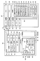
- FIG. 1 shows an information processing apparatus 10 according to the present embodiment.
- the information processing apparatus 10 includes a data management unit 12, an evaluation unit 14, and a command operation unit 22.
- the evaluation unit 14 includes a time management unit 16, an error collection unit 18, and an error analysis unit 20.
- the information processing apparatus 10 is connected to an evaluated unit 24 that is a computer system.
- the evaluated unit 24 performs various processes by each of a plurality of processing units as a computer system.
- the evaluated unit 24 includes a plurality of processing units 26 and a data control unit 28.
- Each of the plurality of processing units 26 is connected to the data control unit 28 via a bus 27 such as a PCI (Peripheral-Component-Interconnect) bus.
- Each of the plurality of processing units 26 includes a storage unit 30 including a first storage unit 32 and a second storage unit 34, a switching unit 36, a control unit 38, and a calculation unit 40.
- symbols A to N are added after the reference numerals to distinguish the processing units 26 or elements from each other. May be handled.
- the information processing apparatus 10 is an example of an information processing apparatus in the disclosed technology
- any one of the plurality of processing units 26 is an example of a processing unit in the disclosed technology.
- the data management unit 12 manages data related to firmware update and evaluation.
- the data management unit 12 stores firmware data for updating firmware and test data for evaluating firmware.
- the data management unit 12 stores the number of firmware to be evaluated and parameters for each firmware evaluation, and can provide information on firmware data, test data, the number of firmware, and parameters for each firmware evaluation.
- the error collection unit 18 collects error information generated during firmware evaluation.
- the error collection unit 18 has a function of displaying the collected error information on a display device or the like.
- the command operation unit 22 outputs a command signal for operating the evaluated unit 24 to the evaluated unit 24.
- command signals include a signal indicating power-on to activate the device (Power_on signal), a signal indicating restart to enable firmware update (Reset signal), and a power-off to stop the operation of the device Signal (Shutdown signal).
- the command operation unit 22 outputs a command signal to the data control unit 28 of the evaluated unit 24.
- the error analysis unit 20 monitors errors that occur in the processing unit 26. For example, the error analysis unit 20 monitors the number and frequency of error occurrences based on information from the error collection unit 18 and the time management unit 16. Further, the error analysis unit 20 may request that the command operation unit 22 output a signal indicating a restart (Reset signal) or a power shutdown signal (Shutdown signal) depending on the result of error monitoring.
- a restart Reset signal
- a power shutdown signal Shut signal
- the data control unit 28 of the evaluated unit 24 controls each of the plurality of processing units 26 based on data and commands from the information processing apparatus 10.
- Each of the plurality of processing units 26 is configured so that the arithmetic unit 40 including a CPU or the like is basically used for hardware resources by firmware stored in the storage unit 30 including the first storage unit 32 and the second storage unit 34 such as a flash memory. Control.
- the control unit 38 outputs various control signals and switches the switching unit 36.
- the switching unit 36 receives the control signal from the control unit 38 and connects the first storage unit 32 and the calculation unit 40 in order to evaluate the firmware stored in the first storage unit 32. Further, the switching unit 36 performs switching so as to connect the second storage unit 34 and the control unit 38 in order to store the data from the control unit 38 in the second storage unit 34.
- the data management unit 12 of the information processing apparatus 10 outputs the first firmware data to the data control unit 28 in order to store the first firmware data of the firmware in the first storage unit 32.
- the data control unit 28 outputs a signal for switching the switching unit 36 in order to store the first firmware data in the first storage unit 32.
- the data management unit 12 of the information processing apparatus 10 indicates a restart to the instruction operation unit 22 so that the plurality of processing units 26 are restarted. Request to output a signal.
- the command operation unit 22 receives a request from the data management unit 12 and outputs a signal indicating restart to the data control unit 28.
- the data control unit 28 receives the signal indicating the restart (Reset signal), resets the switching unit 36, and switches the connection.
- processing by the firmware of the first firmware data is executed by the arithmetic unit 40.
- the data control unit 28 performs error detection.
- the error collection unit 18 of the information processing apparatus 10 collects errors detected by the data control unit 28 as information.
- the data management unit 12 of the information processing apparatus 10 stores the second firmware data in order to store the second firmware data of the firmware in the second storage unit 34.
- the data is output to the data control unit 28.
- the data control unit 28 stores the second firmware data in the second storage unit 34. In this way, by performing firmware update and evaluation in parallel, a plurality of firmware can be evaluated in a short time.
- the information processing apparatus 10 can be realized by, for example, the computer 42 shown in FIG.
- the computer 42 includes a CPU 44, a memory 46, a nonvolatile storage unit 48, an input / output port (I / O) 61, a display 62, a keyboard 63, a mouse 64, and a timer 65.
- the CPU 44, the memory 46, the nonvolatile storage unit 48, the input / output port (I / O) 61, the display 62, the keyboard 63, the mouse 64, and the timer 65 are connected to each other via the bus 60.
- the storage unit 48 can be realized by an HDD (Hard Disk Drive), a flash memory, or the like.
- the storage unit 48 serving as a recording medium stores a test program 50 for causing the computer 42 to function as the information processing apparatus 10. Further, the storage unit 48 stores a web browser (WebBrowser) program 56, a farm data DB 57, a test data DB 58, and an evaluation parameter DB 59, respectively.
- the CPU 44 reads out the web browser program 56 from the storage unit 48, expands it in the memory 46, and executes processing by the web browser program 56. Further, the CPU 44 reads the test program 50 from the storage unit 48 and develops it in the memory 46, and sequentially executes the processes included in the test program 50.
- WebBrowser WebBrowser
- the test program 50 includes a data management process 51, a time management process 52, an error collection process 53, an error analysis process 54, and an instruction operation process 55.
- the CPU 44 operates as the data management unit 12 illustrated in FIG. 1 by executing the data management process 51. That is, the information processing apparatus 10 is realized by the computer 42, and the computer 42 operates as the data management unit 12 illustrated in FIG. 1 by executing the data management process 51.
- the CPU 44 operates as the time management unit 16 illustrated in FIG. 1 by executing the time management process 52.
- a partial area of the memory 46 is used as an area for storing time information obtained by processing of the time management unit 16.
- the CPU 44 operates as the error collection unit 18 shown in FIG. 1 by executing the error collection process 53.
- a partial area of the memory 46 is used as an area for storing error information obtained by the process of the error collection unit 18.
- the CPU 44 operates as the error analysis unit 20 shown in FIG. 1 by executing the error analysis process 54.
- a partial area of the memory 46 is used as an area for storing information indicating an analysis result obtained by the process of the error analysis unit 20.
- the CPU 44 operates as the command operation unit 22 shown in FIG. 1 by executing the command operation process 55.
- the computer 42 that has executed the test program 50 functions as the information processing apparatus 10.
- the storage unit 48 of the computer 42 stores an evaluation parameter DB 59.
- the evaluation parameter DB 59 stores, as one or a plurality of evaluation parameters, information that defines which firmware is to be evaluated with which test data when evaluating the firmware.
- the evaluation parameter includes information that associates firmware data of firmware to be evaluated, test data for evaluating the firmware to be evaluated, and travel time. The travel time is the time for which the CPU is operated by test data for the firmware to be evaluated.
- the evaluation parameter can include the number of errors and the type of error that occur due to the CPU operation by the firmware. When the number of errors and the error type are included in the evaluation parameter, it is preferable that a process to be transferred next is determined by the evaluation parameter corresponding to the number of errors and the error type.
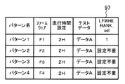
- FIG. 4 shows a first table 97 that is a part of an evaluation plan table that stores, as information, evaluation parameters indicating evaluation contents for evaluating a plurality of firmware.
- FIG. 5 is a diagram of an evaluation plan table that stores, as information, criteria for determining the status transition of firmware evaluation based on errors depending on the type and frequency of errors occurring in the system when systematically evaluating a plurality of firmwares.
- the 2nd table 98 which is a part is shown.
- Fig. 4 shows an example when four types of firmware are systematically evaluated. That is, a table in which the pattern name, firmware, travel time setting, test data, and LFWH (Local Firmware Hub) 0_BANK_sel are associated with each other and are arranged in the order of the evaluation plan can be employed.
- the pattern name is a name for identifying an evaluation parameter group in which firmware, travel time setting, test data, and LFWH0_BANK_sel information are associated with each other.
- the information of the item LFWH0_BANK_sel stores the value of information for switching the bus switch included in the system board whose details will be described later. For example, when the pattern name is “pattern 1” in the first table 97 shown in FIG.
- the firmware evaluation is executed in the order of the pattern 1.2.3.4.
- FIG. 5 shows an example of criteria for determining the status transition of firmware evaluation according to the type and frequency of errors that occur during firmware evaluation.
- FIG. 5 shows an example in which three types of information, ie, CE (Correctable Error), UE (Uncorrectable Error), and FE (Fetal Error), which are information indicating error contents, are used with the error type as the error type item. Show.
- the information CE indicating the error content is, for example, a 1-bit error indicated by the CPU or processor.
- the information UE indicating the error content is, for example, a 2-bit error indicated by the CPU or the processor.
- the information FE indicating the error content is a fatal error such as an internal error or a bus error indicated by the CPU or processor.
- Information in which the frequency of error notification is associated with information CE, UE, and FE indicating error contents is assigned.
- the information UE indicating the error content is “evaluation continuation” when the UE occurs once, “Shutdown” when the UE occurs twice in one minute, “firmware” when the UE occurs twice in 10 minutes, for example.
- Information indicating “switching” is given. That is, information indicating the criteria for determining the state transition of firmware evaluation that the firmware evaluation is continued when the UE occurs once during the running time is the content of the error that occurs during the firmware evaluation.
- test program 50 is an example of an information processing program in the disclosed technology. That is, the test program 50 is an example of an information processing program for causing the computer 42 to function as the information processing apparatus 10.
- the evaluated unit 24 can be realized by, for example, the computer system 70 shown in FIG.
- the computer system 70 includes a plurality of system boards (hereinafter referred to as SB) 84 and a system control board 72.
- SB system boards
- the system can function as a system called a domain having a configuration in which a plurality of SBs 84 are regarded as a functional unit that performs processing combined by a plurality of SBs 84.
- the symbols A to N are added to the symbols and described.
- Each of the plurality of SBs 84 included in the computer system 70 includes a system management controller (Baseboard Management Controller, hereinafter referred to as BMC) 86 and a CPU 90.
- BMC System Management Controller
- Each of the plurality of SBs 84 includes a bus switch (Bus-Exchange) 92 and a local flash memory 94.
- the local flash memory 94 is expressed as LFWH0.
- the local flash memory 94 is a memory for storing firmware, and includes a first memory 95 and a second memory 96 in the present embodiment.
- the first memory 95 is expressed as LFWH0_A.
- the second memory 96 is denoted as LFWH0_B.
- the system control board 72 of the computer system 70 corresponds to the data control unit 28 shown in FIG.
- the SB 84 included in the computer system 70 corresponds to the processing unit 26 shown in FIG.
- the BMC 86 of the SB 84 corresponds to the control unit 38 shown in FIG.
- the CPU 90 corresponds to the calculation unit 40 shown in FIG.
- the bus switch 92 corresponds to the switching unit 36 shown in FIG.
- the local flash memory 94 corresponds to the storage unit 30 shown in FIG.
- the first memory 95 corresponds to the first storage unit 32 shown in FIG. 1, and the second memory 96 corresponds to the second storage unit 34 shown in FIG.
- the SB 84 includes one CPU 90
- the number of CPUs is not limited to one and may be two or more.
- the local flash memory 94 will be described as a local flash memory 94 having two storage areas in which different firmware can be stored in the first memory 95 and the second memory 96.
- the storage area in which the firmware can be stored in the local flash memory 94 is not limited to two, and may be three or more.
- a CPU 90 is connected to the BMC 86 via a serial parallel interface bus (hereinafter referred to as SPI_BUS) 89.
- a bus switch 92 is connected to the BMC 86 via a serial parallel interface bus (hereinafter referred to as SPI bus) 88 and a serial bus 87.
- SPI bus serial parallel interface bus
- I2C bus Inter-Integrated Circuit Bus
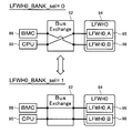
- the bus switch 92 is connected to the local flash memory 94 and switches the connection between the BMC 86 and the CPU 90 and the first memory 95 and the second memory 96 of the local flash memory 94 by a control signal from the serial bus 87.
- the bus switch 92 has a function of switching between the first switching state and the second switching state.
- the first switching state is a state in which the BMC 86 is connected to the first memory 95 via the SPI bus 88 and the CPU 90 and the second memory 96 are connected.
- the second switching state is a state in which the BMC 86 is connected to the second memory 96 via the SPI bus 88 and the CPU 90 and the first memory 95 are connected.
- the BMC 86 also includes a memory BMC_M such as an EEPROM (Electrically-Erasable-Programmable-Read-Only Memory).
- the memory BMC_M stores information indicating whether firmware can be updated (hereinafter referred to as information LFWH0_update), and information for switching the bus switch 92 (hereinafter referred to as information LFWH0_BANK_sel). For example, as an example of the value of the information LFWH0_update, “1” is stored when the firmware is updated, and “0” is stored when the firmware update is prohibited.
- the information LFWH0_BANK_sel is information for setting the connection destination of the CPU 90 and the BMC 86 and the first memory 95 and the second memory 96.
- the system control board 72 included in the computer system 70 includes a CPU 78, a memory 79, a nonvolatile storage unit 74, an input / output port (I / O) 77, and a bus interface (I / F) 80 such as a PCI bus.
- the CPU 78, the memory 79, the nonvolatile storage unit 74, the input / output port (I / O) 77, and the bus interface (I / F) 80 are connected to each other via a bus 81.
- the storage unit 74 stores a control program 75 and a web user interface program 76. In FIG. 2, the web user interface program 76 is represented as WebUI_PG.
- the CPU 78 reads out the control program 75 and the web user interface program 76 from the storage unit 74, loads them into the memory 79, and executes processing by the control program 75 and the web user interface program 76.
- the bus interface 80 of the system control board 72 is connected to each of the BMCs 86 of the plurality of SBs 84 via the PCI bus 82. Further, the input / output port 77 is connected to the input / output port 61 via a LAN (Local Area Network) 68, so that the computer 42 and the computer system 70 are connected so as to be able to exchange information.
- the system control board 72 operates as the data control unit 28 shown in FIG. 1 when the CPU 78 executes the control program 75 and the web user interface program 76.
- firmware update and evaluation are performed in parallel using the first memory 95 (LFWH0_A) and the second memory 96 (LFWH0_B) for storing the firmware of the SB84.
- a test for quality assurance is performed, but a hardware or firmware failure occurs, the firmware is recreated each time, and a long evaluation time is required.
- a plurality of firmware may be prepared and the optimum firmware may be determined based on the evaluation result.
- firmware update and firmware evaluation are executed alternately (serially), the time required for processing increases according to the number of firmware to be updated and evaluated. Therefore, in this embodiment, a plurality of storage areas for storing firmware are prepared, and firmware update and evaluation are performed in parallel, thereby reducing the time required for firmware evaluation.
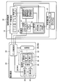
- FIG. 6 shows the relationship between the units included in the information processing apparatus 10 and the relationship between the units included in the evaluated unit 24.
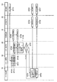
- FIG. 7 shows a flow of processing related to each unit of the information processing apparatus 10 as a sequential flow.
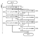
- FIG. 8 is a diagram for explaining that the time can be shortened by updating and evaluating a plurality of firmwares.
- FIG. 9 shows a flow of processing related to each unit of the information processing apparatus 10 when an error occurs in the evaluated unit 24 as a sequential flow.
- the firmware data and test data of the firmware to be evaluated are stored in the data management unit 12.
- the data management unit 12 transmits firmware data and test data of the firmware to be evaluated to the processing unit 26 installed in the evaluated unit 24 (see also FIG. 6).
- the data management unit 12 instructs the command operation unit 22 to perform a restart instruction for restart (Reset) for enabling the firmware, or power shutdown (Shutdown) for stopping the operation of the device when all the firmware evaluations are completed.
- a power-off instruction is output (see also FIG. 6).
- the data management unit 12 instructs the command operation unit 22 to turn on the information processing apparatus 10 in order to cause the evaluated unit 24 (at least the processing unit 26) to turn on the power (see FIG. 7 step SF01).
- the command operating unit 22 commands the evaluated unit 24 to turn on the power in response to an instruction from the data management unit 12 (step SF02).
- the evaluated unit 24 receives the command from the command operating unit 22 and executes power-on (step SF03). In other words, the evaluated unit 24 executes a process in which the data control unit 28 of the evaluated unit 24 receives a command from the command operating unit 22 and powers on the entire apparatus including at least the processing unit 26.
- the data management unit 12 transmits information indicating whether the first firmware update is performed in the first storage unit 32 or the second storage unit 34.
- the data management unit 12 transmits the LFWH0_BANK_sel signal (here, a signal of value “1”) based on the information of LFWH0_BANK_sel in the first table 97 to the evaluated unit 24 based on the information in the evaluation plan table (step S40).
- the data control unit 28 of the evaluated unit 24 receives the LFWH0_BANK_sel signal transmitted from the data management unit 12, and switches the switching unit 36 of the processing unit 26 (step SF05).
- the processing unit 26 of the evaluated unit 24 executes processing up to the state for updating the firmware (step SF06).
- the process of step SF06 is a process of starting up until the operating system is activated.
- the data management unit 12 transmits the value “1” of the information LFWH0_update to the evaluated unit 24 so that the processing unit 26 can update the firmware (step SF07).
- the to-be-evaluated part 24 performs the process which makes the firmware update possible in the process part 26 (step SF08). That is, in the evaluated unit 24, the data control unit 28 receives information LFWH0_update from the data management unit 12. Then, the data control unit 28 sets the value “1” of the information LFWH0_update in the control unit 38, so that the firmware data can be written into the first storage unit 32 of the processing unit 26.
- the data management unit 12 transmits the firmware data of the first firmware to the evaluated unit 24 (step SF09).
- the evaluated unit 24 After receiving firmware firmware data from the data management unit 12, the evaluated unit 24 updates the firmware (step SF10).
- the data control unit 28 receives the firmware data of the first firmware and writes the firmware data to the first storage unit 32 via the control unit 38.
- the data control unit 28 notifies the data management unit 12 that the firmware update is completed (step SF11).
- the data management unit 12 sets the value “0” of the information LFWH0_update to be in a state in which the firmware cannot be updated after the first firmware update is completed in the processing unit 26 when the first firmware update is completed. It transmits to the to-be-evaluated part 24 (step SF12).
- the to-be-evaluated part 24 performs the process which makes the firmware update impossible in the process part 26 (step SF13). Further, the data management unit 12 instructs the instruction operation unit 22 to restart the processing unit 26 of the evaluated unit 24 in order to validate the updated first firmware (step SF14).
- the command operation unit 22 receives an instruction from the data management unit 12, and transmits a restart command to the evaluated unit 24 (step SF15).
- the evaluated unit 24 (data control unit 28) receives the restart command from the command operating unit 22, and restarts the processing unit 26 (step SF16).
- the state of the bus switch 92 is switched by restarting the processing unit 26 of the evaluated unit 24 (see also FIG. 3). In other words, it becomes possible for the computing unit 40 to operate with firmware based on the firmware data written in the first storage unit 32, that is, the computing unit 40 can execute the firmware data.
- the processing unit 26 is restarted to execute processing up to the state for performing the firmware evaluation (OS_boot: processing to start up until the operating system is activated (step SF17)).
- OS_boot processing to start up until the operating system is activated
- the data management unit 12 transmits the test data to the data control unit 28 of the evaluated unit 24 (step SF18).
- the test data received by the data control unit 28 from the data management unit 12 is transmitted to the calculation unit 40 via the control unit 38.
- the calculation unit 40 performs firmware evaluation using the test data from the data management unit 12 (step SF19).
- the data management unit 12 transmits information indicating that the firmware evaluation has started to the time management unit 16 (step SF20).
- the time management unit 16 receives the information from the data management unit 12 and records the evaluation start time (step SF21).
- the time management unit 16 transmits the recorded evaluation start time to the error analysis unit 20 (step SF22).
- the error analysis unit 20 acquires the evaluation start time (step SF23), and starts analysis for error analysis. For example, measurement of travel time is started.
- the data management unit 12 determines whether or not there is unevaluated firmware (step SF24). When there is unevaluated firmware, the data management unit 12 proceeds to a process for updating the next firmware. That is, the data management unit 12 transmits the value “1” of the information LFWH0_update to the evaluated unit 24 so that the processing unit 26 can update the next firmware (step SF25). The evaluated unit 24 executes processing for making the next firmware updateable in the processing unit 26 (step SF26). Further, the data management unit 12 transmits the firmware data of the next firmware to the evaluated unit 24 (step SF27). The evaluated unit 24 receives the firmware data transmitted by the data management unit 12, and executes the next firmware update (step SF10). That is, in the evaluated unit 24, the data control unit 28 receives the firmware data of the next firmware, and writes the firmware data to the second storage unit 34 via the control unit 38.
- the data control unit 28 When the next firmware update is completed in the processing unit 26, the data control unit 28 notifies the data management unit 12 that the next firmware update is completed (step SF29).
- the data management unit 12 transmits the value “0” of the information LFWH0_update to the evaluated unit 24 so that the processing unit 26 cannot update the firmware when the next firmware update is completed ( Step SF30).
- the to-be-evaluated part 24 performs the process which makes the update of a firmware impossible in the process part 26 (step SF31).
- the data management unit 12 transmits the travel time set in the first table 97 to the time management unit 16 for the first firmware evaluation (step SF32).
- the time management unit 16 receives the travel time from the data management unit 12 (step SF33), performs time management (monitoring) until the received travel time elapses, and passes the travel time to the data management unit 12 when the travel time elapses. Notification is made (step SF34).
- the data management unit 12 receives the notification of the elapsed travel time from the time management unit 16 and considers that the end of the evaluation has been notified (step SF37).
- the data management unit 12 transmits an evaluation parameter related to the firmware evaluation to the error analysis unit 20 (step SF35).
- the error analysis unit 20 acquires the evaluation parameter transmitted from the data management unit 12 (step SF36), and uses the evaluation parameter for error analysis.
- the data management unit 12 instructs the command operation unit 22 to stop the operation of the processing unit 26 when there is no unevaluated firmware and all the evaluations are completed (step SF38).
- the command operation unit 22 receives an instruction from the data management unit 12, and transmits a power-off command to the evaluated unit 24 (step SF39).
- the evaluated unit 24 receives the power-off command from the command operating unit 22, and shuts off the power of the evaluated unit 24 (step SF40).
- the data management unit 12 may wait for the evaluation to end.
- step SF37 If there is unevaluated firmware after step SF37, the process returns to step SF14 and the above processing is repeated.
- the information processing apparatus 10 can perform update and evaluation in parallel for a plurality of firmware, and can shorten the time for evaluating the plurality of firmware. That is, when the evaluation plan according to the first table 97 shown in FIG. 4 is executed, first, as shown in FIG. ) Is updated (step ST1).
- the firmware (F1) is updated to the first storage unit 32 of the processing unit 26.
- the information processing apparatus 10 executes the evaluation of the firmware (F1) (step ST2), and executes the update of the firmware (F2) by the pattern 2 in parallel with the process of step ST2 (step ST3).
- the firmware (F2) is updated to the second storage unit 34 of the processing unit 26. Since the information processing apparatus 10 uses the first storage unit 32 and the second storage unit 34 included in the first storage unit 32 to update and evaluate the firmware, the firmware (F1) evaluation and the firmware ( Wait until both processes of F2) are completed.
- the information processing apparatus 10 executes the update of the firmware (F3) by the pattern 3 to the evaluated unit 24 (step ST4). ).
- the firmware (F3) is updated to the first storage unit 32 of the processing unit 26.
- the information processing apparatus 10 executes the evaluation of the firmware (F2) (step ST5).
- the second storage unit 34 of the processing unit 26 is used. The information processing apparatus 10 waits until both processing of firmware (F2) evaluation and firmware (F3) update is completed.
- the information processing apparatus 10 executes the firmware (F3) evaluation (step ST6).
- the firmware (F4) is updated by the pattern 4 (step ST7).
- the firmware (F4) is updated to the second storage unit 34 of the processing unit 26.
- the information processing apparatus 10 waits until both processing of firmware (F3) evaluation and firmware (F4) update is completed.
- the information processing apparatus 10 executes the firmware (F4) evaluation (step ST8) and ends the evaluation of all the firmware.
- processing of firmware (F1) evaluation (step ST2) and firmware (F2) update (step ST3) are performed in parallel. Therefore, both processes are completed in the longer time (time t2) of the time required for the evaluation of the firmware (F1) and the time required for updating the firmware (F2). Further, the processes of the firmware (F2) evaluation (step ST5) and the firmware (F3) update (step ST4) are performed in parallel. For this reason, both processes are completed in the longer time (time t4) of the time required for the firmware (F2) evaluation and the time required for the firmware (F3) update. Further, the processes of the firmware (F3) evaluation (step ST6) and the firmware (F4) update (step ST7) are performed in parallel. For this reason, both processes are completed in the longer time (time t6) of the time required for the evaluation of the firmware (F3) and the time required for the update of the firmware (F4).
- the sum of the time required for the evaluation of the four different firmwares is the sum of the longer time in each parallel processing (t1 + t2 + t4 + t6 + t8 in the example of FIG. 8), and when the firmware update and evaluation processes are repeated alternately. It can be shortened in comparison.
- the evaluated unit 24 transmits error information to the error collecting unit 18 (step SF41).
- the error collecting unit 18 receives error information from the evaluated unit 24 (step SF43), and notifies the time management unit 16 of information indicating that an error has occurred in the evaluated unit 24 (step SF44).
- the time management unit 16 records the timing at which the notification of error occurrence from the error collection unit 18 is received (triggered) as the error occurrence time (step SF45).
- the time management unit 16 transmits the recorded error occurrence time to the error analysis unit 20 (step SF46).
- the error analysis unit 20 acquires the error occurrence time transmitted from the time management unit 16 (step SF49).
- the error collection unit 18 transmits information indicating the content of the generated error to the error analysis unit 20 together with the notification of the occurrence of the error (step SF47).
- the error analysis unit 20 identifies information indicating the content of the error transmitted from the error collection unit 18 (step SF48).
- the error analysis unit 20 performs analysis on the error using the identified error content and the acquired error occurrence time (step SF50). Analysis for errors is performed using the number of errors, the frequency of occurrence of errors, and evaluation parameters.
- the data management unit 12 sets the processing unit 26 of the evaluated unit 24 at the timing when the firmware update processing being executed in parallel ends.
- Restart That is, the data management unit 12 instructs the command operation unit 22 to give a command to restart the processing unit 26 (step SF52).
- the command operation unit 22 receives an instruction from the data management unit 12, and transmits a restart command to the evaluated unit 24 (step SF53).
- the evaluated unit 24 (data control unit 28) receives the restart command from the command operating unit 22, and restarts the processing unit 26 (step SF54).
- the data management unit 12 issues an instruction to immediately stop the operation of the processing unit 26 of the evaluated unit 24 (Shutdown).
- the operation unit 22 is instructed (step SF55).
- the command operation unit 22 receives an instruction from the data management unit 12, and transmits a power-off command to the evaluated unit 24 (step SF56).
- the evaluated unit 24 receives the power-off command from the command operation unit 22, and shuts off the power of the evaluated unit 24 to stop at least the operation of the processing unit 26 (step SF57).
- SB84A SB84A
- the CPU 44 of the computer 42 executes each process included in the test program 50 stored in the storage unit 48. That is, the CPU 44 of the computer 42 expands the data management process 51, time management process 52, error collection process 53, error analysis process 54, and command operation process 55 stored in the test program 50 of the storage unit 48 in the memory 46. Execute. As a result, the processing routines shown in FIGS. 10 to 16 are executed.
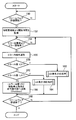
- FIG. 10 is a flowchart showing the flow of processing in the data management unit 12.
- the information processing apparatus 10 is realized by the computer 42, and the computer 42 operates as the data management unit 12 (FIG. 1) by developing the data management process 51 in the memory 46 and executing it by the CPU 44.
- the firmware data of the firmware to be evaluated is stored in the firmware data DB 57, and the test data is stored in the test data DB 58.
- step 100 in order to turn on the computer system 70, the instruction operation process 55 (instruction operation unit 22) is instructed to turn on the computer system 70.
- step 102 based on the information in the evaluation plan table, the value based on the information of LFWH0_BANK_sel in the first table 97 (here, the value “1”) is transmitted to the computer system 70 as the LFWH0_BANK_sel signal.
- step 104 the computer system 70 waits until the firmware can be updated, and the process proceeds to step 106.
- the system control board 72 receives the LFWH0_BANK_sel signal via the input / output port 77, and the bus switch 92 of the SB 84 is switched.
- the SB 84 of the computer system 70 executes a process (OS_boot: process for starting up the operating system) up to a state where the firmware can be updated.
- OS_boot process for starting up the operating system
- the first memory 95 and the second memory 96 of the local flash memory 94 are alternately connected by setting and resetting the bus switch 92 as will be described later, so that information on LFWH0_BANK_sel There is no need to set the value by.
- the value “1” of the information LFWH0_update is transmitted to the computer system 70 so that the firmware can be updated in SB84.
- the system control board 72 receives the value of the information LFWH0_update and sets it in the BMC 86 of the SB84. When the value of the information LFWH0_update is set in the BMC 86, the first memory 95 of the SB 84 becomes ready to write firmware data.
- the firmware data of the first firmware is transmitted to the computer system 70. When the firmware data of the first firmware is transmitted, the update of the first firmware is started in SB84.
- the system control board 72 receives the first firmware firmware data and writes the first firmware data to the first memory 95 via the BMC 86.
- step 110 the firmware is updated.
- step 114 the storage of data in the local flash memory 94 is prohibited (the firmware cannot be updated) with the end of the first firmware update, so that the value “0” of the information LFWH0_update is set to the computer system 70.
- the system control board 72 receives the value of the information LFWH0_update and sets it in the BMC 86 of the SB84. As a result, the first memory 95 of the SB 84 becomes unable to write firmware data.
- next step 116 in order to validate the updated first firmware, an instruction to the instruction operation process 55 (instruction operation unit 22) is executed so that an instruction to restart (reset) the SB 84 of the computer system 70 is executed. .
- the command operation process 55 receives an instruction from the data management process 51 and transmits a restart command to the computer system 70.
- the process waits until the computer system 70 can evaluate the firmware, that is, until the OS is in the operating state in SB 84, and proceeds to step 120.
- next step 122 it is determined whether there is unevaluated firmware. This determination can be made from the total number of firmware data registered in the data management process 51. If the determination in step 122 is affirmative, the process proceeds to step 124, and the value “1” of the information LFWH0_update is transmitted to the computer system 70 so that the next firmware can be updated. In the next step 126, update of the next firmware is started by transmitting the firmware data of the next firmware.
- step 130 transmission of the firmware data of the firmware is continued (until affirmative determination is made in step 130) until transmission to the computer system 70 is completed (step 128), and firmware update is executed.
- step 130 an affirmative determination is made in step 130 and the firmware update is released in step 132. That is, in step 132, the value “0” of the information LFWH0_update is transmitted to the computer system 70.
- step 134 negative determination is repeated until the evaluation of the firmware under evaluation is completed. If the determination in step 134 is affirmative, the process proceeds to step 136, and it is determined whether or not the evaluation of all the firmware set in the first table 97 has been completed. When all the firmware evaluations have been completed, an affirmative determination is made at step 136 and the process proceeds to step 138 to instruct the instruction operation process 55 (instruction operation unit 22) to give an instruction to stop the operation of the computer system 70. As will be described later, the command operation process 55 transmits a power-off command to the computer system 70 to shut down the computer system 70. On the other hand, if the determination in step 136 is negative, there is firmware that has not been evaluated, so the process returns to step 116 and the above process is repeated.
- FIG. 11 is a flowchart showing the flow of processing in the error collection process 53.
- the information processing apparatus 10 is realized by the computer 42, and the error collection process 53 is expanded in the memory 46 and executed by the CPU 44, whereby the computer 42 operates as the error collection unit 18 (FIG. 1).
- the error collection process 53 acquires error information from the system control board 72 when an error occurs during the evaluation of the firmware, transmits the error content to the error analysis process 54 (error analysis unit 20), and that an error has occurred. Is transmitted to the time management process 52 (time management unit 16).
- step 140 the process waits until a notification indicating that the firmware evaluation has started is started.
- the process proceeds to step 141.
- step 141 the presence / absence of an error in SB84 is detected, and in step 142, it is determined whether an error has occurred in SB84. That is, whether or not an error has occurred in the system control board 72 is detected by polling processing (polling) at step SB84.
- the information processing apparatus 10 is realized by the computer 42, and the computer 42 operates as the error analysis unit 20 (FIG. 1) when the error analysis process 54 is expanded in the memory 46 and executed by the CPU 44.
- the error process 54 performs error analysis processing using the error information transmitted from the error collection process 53 (error collection unit 18). That is, the error analysis process 54 performs processing on error contents (CE, UE, FE) from the error information, the firmware evaluation start time acquired from the time management process 52 (time management unit 16), and the time when the error occurred. Do.
- step 150 the process waits until a notification indicating that the evaluation of the firmware has started is started.
- the process proceeds to step 152.
- step 152 the start time of firmware evaluation is acquired from the time management process 52 (time management unit 16).
- step 154 negative determination is repeated until error information is received from the error collection process 53 (error collection unit 18).
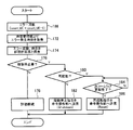
- Step 156 it is identified whether the error content is CE, UE, or FE.
- Step 158 it is determined whether or not the content of the error is CE. If the determination in step 158 is affirmative, the process proceeds to step 168 after executing the process of step 160.
- step 162 determines whether or not the content of the error is UE. If the determination in step 162 is affirmative, the process proceeds to step 168 after executing the process of step 164.
- step 166 transmits a power shutdown command to the computer system 70 to the command operation process 55 (command operation unit 22). 70 is turned off. Note that in step 166, it may be instructed to transmit information requesting the power-off of the computer system 70 to the data management process 51 (data management unit 12). In this case, it is possible to instruct the power management command to be transmitted from the data management process 51 (data management unit 12) to the command operation process 55 (command operation unit 22).
- step 168 it is determined whether or not the firmware evaluation is completed. Step 168 is unconditionally affirmed when step 166 is passed. When the process passes through step 160, a determination is made on the result of the process described later in step 160. Similarly, when the process goes through step 164, a determination corresponding to the result of the process described later in step 164 is made. If an affirmative determination is made in step 168, this processing routine is terminated. If a negative determination is made, the process returns to step 154. If a firmware evaluation end notification is made between steps 152 to 166, the processing routine can be ended assuming that an affirmative determination is made in step 168 as an interrupt process.
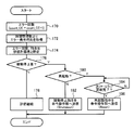
- step 160 of FIG. 12 when the error content is CE, the processing routine shown in FIG. 13 is executed.
- step 172 the current time is acquired from the time management process 52 (time management unit 16), and the error occurrence time is acquired every time an error occurs.
- step 174 the error occurrence time interval obtained in step 172 is obtained, and the error frequency obtained in step 170 and the error occurrence frequency according to the obtained error occurrence time interval are collated with the evaluation plan table. That is, it collates with each information of the error type “CE” in the second table 98.
- step 176 it is determined whether or not the computer system 70 needs to be stopped using the collation result in step 174. If a negative determination is made in step 176, information indicating that the firmware evaluation is continued is set in step 178, and this routine is terminated. Information indicating that the firmware evaluation is continued is used for the determination in step 168 of FIG.
- step 176 when an affirmative determination is made in step 176, the process proceeds to step 180, and it is determined whether or not the collation result in step 174 is information indicating restart.
- step 180 an instruction to cut off the power supply of the computer system 70 is transmitted to the command operation process 55 (command operation unit 22), and the power supply of the computer system 70 is cut off.
- step 166 information for requesting power-off of the computer system 70 may be transmitted to the data management process 51 (data management unit 12). In this case, a power-off instruction can be transmitted from the data management process 51 (data management unit 12) to the command operation process 55 (command operation unit 22).
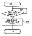
- step 180 If the determination in step 180 is affirmative, the process waits until the next firmware update is completed (negative determination is repeated in step 184). When the update of the next firmware is completed (when an affirmative determination is made in step 184), the process proceeds to step 186, and an instruction to restart the SB 84 of the computer system 70 is transmitted to the instruction operation process 55 (instruction operation unit 22). Then, the SB 84 of the computer system 70 is restarted.
- step 186 information for requesting restart of the SB 84 of the computer system 70 may be transmitted to the data management process 51 (data management unit 12). In this case, a restart instruction can be transmitted from the data management process 51 (data management unit 12) to the command operation process 55 (command operation unit 22).
- step 164 of FIG. 12 when the error content is UE, the processing routine shown in FIG. 14 is executed.
- the process in FIG. 14 is almost the same as the process in FIG.
- the difference between the process of FIG. 14 and the process of FIG. 13 is that the error content is “CE” or the error content is “UE”.
- step 188 in FIG. 14 the error content can be realized by replacing “CE” with “UE”.
- FIG. 15 is a flowchart showing the flow of processing in the time management process 52.
- the computer 42 operates as the time management unit 16 (FIG. 1).
- the time management process 52 records the firmware evaluation start time and error occurrence time, acquires the firmware evaluation time from the data management process 51 (data management unit 12), and determines the error occurrence time as the error analysis process 54 ( To the error analyzer 20).
- step 200 the process waits until a notification indicating that the evaluation of the firmware has started is started.
- the process proceeds to step 202.
- step 202 the firmware evaluation start time is recorded.
- the start time can be obtained by referring to the timer 65 and acquiring the current time.
- step 212 it is determined whether or not the travel time acquired in step 204 has elapsed. If a negative determination is made in step 212, the process returns to step 206. If an affirmative determination is made, the process proceeds to step 214.
- the running time has elapsed, it is a time when the evaluation of the firmware has been completed, and therefore information indicating the end of the evaluation is transmitted to the data management process 51 (data management unit 12) in step 214.
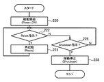
- FIG. 16 is a flowchart showing the flow of processing in the command operation process 55.
- the information processing apparatus 10 is realized by the computer 42, and the instruction operation process 55 is expanded in the memory 46 and executed by the CPU 44, whereby the computer 42 operates as the instruction operation unit 22 (FIG. 1).
- the command operation process 55 can transmit a power-on command for the entire computer system 70 to the computer system 70. Further, in the command operation process 55, a restart command and a shutdown command instructed by the data management process 51 (data management unit 12), the error analysis process 54 (error analysis unit 20) are provided. To the computer system 70.
- step 220 a power-on command for the entire computer system 70 that is instructed by the data management process 51 (data management unit 12) and the error analysis process 54 (error analysis unit 20) is output to the computer system 70.
- the operation of the computer system 70 is started when the computer system 70 receives a power-on command.
- step 222 it is determined whether or not a restart instruction has been issued from the data management process 51 (data management unit 12) or the error analysis process 54 (error analysis unit 20). If the result in step 222 is affirmative, a restart command signal is output to the computer system 70 in step 224, and the process returns to step 222.
- step 226 it is determined in step 226 whether or not a power shutdown instruction has been issued from the data management process 51 (data management unit 12) or the error analysis process 54 (error analysis unit 20). . If the determination in step 226 is negative, the process returns to step 222. If the determination is affirmative, in step 228, a power-off command signal is output to the computer system 70, and this routine is terminated.
- firmware that is different from the firmware under evaluation can be updated.
- firmware evaluation firmware updates that are different from the firmware being evaluated are processed, thereby reducing the time required for firmware evaluation compared to alternating firmware updates and evaluations.
- Can do For example, in the case of evaluating four types of firmware, a case where a processing time of 1 hour is required for firmware update and a processing time of 2 hours is required for firmware evaluation is taken as an example. In the technique of continuously processing each update and evaluation process for each of the four types of firmware, 12 hours are required for the entire evaluation. On the other hand, in this embodiment, since parallel processing is possible, all evaluations can be completed in a processing time of 9 hours.
- the firmware evaluation time due to the occurrence of an error. For example, if it can be determined that the significance of continuing the evaluation process has been lost due to the error type, error occurrence frequency, and error occurrence location, the evaluation is terminated before the set evaluation time (running time) elapses. When the evaluation ends before the set evaluation time elapses, it is possible to perform hardware maintenance by temporarily shutting down the next firmware evaluation or power supply, and the firmware evaluation time can be shortened. become.
- the firmware evaluation time can be shortened.
- FIG. 17 shows, as an example, an evaluation table 99 that explicitly provides a firmware operation result to a user who operates the information processing apparatus 10.
- the evaluation table 99 is obtained by adding, to the first table 97, information in which the number of errors that have occurred, the evaluation start time, and the end time are associated with evaluation parameters.
- the evaluation table 99 can explicitly provide evaluation results of a plurality of firmware to a user who operates the information processing apparatus 10.
- FIG. 18 shows the second table 98 (1).
- the second table 98 (1) is obtained by omitting a criterion relating to the frequency of error occurrence as a criterion for determining the state transition of firmware evaluation. More specifically, the second table 98 (1) is information only when there is an error notification, instead of the frequency of error occurrence in the second table 98, and information indicating error contents (CE, UE, FE) Information indicating the status transition of the firmware evaluation associated with the information).
- CE error contents
- the difference between the second embodiment and the first embodiment is the processing in the error analysis process 54 and the processing in the time management process 52.
- the processing routine of FIG. 19 is executed instead of the processing routine of FIG.
- the processing routine of FIG. 20 is executed instead of the processing routine of FIG.
- the processing routine of FIG. 21 is executed instead of the processing routine of FIG.
- differences will be described.
- step 160 and step 164 of FIG. 12 is processed only by step 161 of FIG. That is, when the content of the error is CE or UE, step 161 is executed.
- FIG. 13 the difference between FIG. 13 and FIG. 20 is that the processing of FIG. 20 processes only the processing of step 184 and step 186 of FIG. That is, when the content of the error is CE or UE, the process waits until the next firmware update is completed (determination is negative in step 184). When the next firmware update is completed (when an affirmative determination is made in step 184), the process proceeds to step 186, and an instruction to restart the SB 84 of the computer system 70 is transmitted to the instruction operation process 55 (instruction operation unit 22). Then, the processing routine of FIG.
- step 212 in FIG. 15 is executed. That is, in the process of FIG. 21, when the determination process of step 206 is negative, the determination of the elapsed travel time at step 212 of FIG. If a negative determination is made in step 211, the process returns to step 206, and if an affirmative determination is made, the process proceeds to step 214. When the process of step 210 is completed, the process proceeds to step 214.
- the evaluation process when an error occurs even once, the evaluation process is terminated to switch to the next firmware evaluation.
- firmware update and evaluation that do not cause an error can be realized. Further, if an error occurs even once, the evaluation is switched to the next firmware evaluation, so that the evaluation time can be further shortened.
- the criterion for the case where there is an error notification is set as the second table 98 which is a part of the evaluation plan table indicating the criterion for determining the state transition of firmware evaluation.
- the second table 98 which is a part of the evaluation plan table indicating the criterion for determining the state transition of firmware evaluation.
- a modified example of the second table 98 will be described as a third embodiment with reference to FIGS. Since the third embodiment has substantially the same configuration as the first and second embodiments, the same parts are denoted by the same reference numerals and detailed description thereof is omitted.
- FIG. 22 shows an example of the second table 98 (2).
- the second table 98 (2) is obtained by adding a criterion when there is no error notification to the second table 98 of FIG. 5 as a criterion for determining the state transition of the firmware evaluation.
- information indicating the status transition of firmware evaluation when there is no error notification is replaced with information (CE, UE, FE) indicating error contents, instead of the frequency of error occurrence. Associating and storing.
- the difference between the third embodiment and the first embodiment is the processing in the time management process 52. Specifically, the processing routine of FIG. 23 is executed instead of the processing routine of FIG. Hereinafter, differences will be described.
- step 204 As processing in the time management process 52, the difference between FIG. 15 and FIG. 23 is that processing related to the occurrence of no error is added to the processing in FIG. That is, in the process of FIG. 23, when the process of step 204 is completed, the process proceeds to step 206 after counting the error-free time in step 230. Further, when a negative determination is made at step 206, it is determined whether or not the error-free state at step 232 has passed one hour. If a negative determination is made in step 232, the process proceeds to step 212, and if an affirmative determination is made, the process proceeds to step 214. When the process of step 210 is completed, the time count when an error has not occurred is reset (set to an initial value, for example, “0”), and then the process proceeds to step 214.
- the firmware to be evaluated is regarded as satisfying a predetermined constant evaluation criterion, and switching to the next firmware evaluation is performed.
- the evaluation process ends.
- the program in the disclosed technology can be provided in a form recorded on a recording medium such as a CD-ROM or a DVD-ROM.
Landscapes
- Engineering & Computer Science (AREA)
- Theoretical Computer Science (AREA)
- Computer Hardware Design (AREA)
- Quality & Reliability (AREA)
- Physics & Mathematics (AREA)
- General Engineering & Computer Science (AREA)
- General Physics & Mathematics (AREA)
- Stored Programmes (AREA)
- Debugging And Monitoring (AREA)
Abstract
1つの側面では、情報処理装置において、ファームウェアの評価時間を短縮する。 データ管理部12は、第1ファームウェアを第1格納部32に、データ制御部28及び切替部36を介して格納させる。第1ファームウェアを有効化するため、命令操作部22は処理部26を再起動させ、切替部36の接続を切り替え、第1ファームウェアを評価時すると共に、該評価中に、第2ファームウェアを第2格納部34に格納させる。ファームウェアの更新と評価を並列処理することにより、複数のファームウェアを短時間で評価することができる。
Description
本発明は、情報処理装置、情報処理方法、情報処理プログラム、及び記録媒体に関する。
コンピュータシステムは、接続されている記憶装置、キーボードやディスプレイ等の入出力装置などのデバイスを制御するBIOS(Basic Input Output System)を含む、ファームウェアを有している。ファームウェアは、システムの構成情報を保持する等によって、コンピュータシステムに含まれるハードウェア資源の機能を最大限に発揮させるハードウェア資源の基本的な制御を行うソフトウェアである。例えば、新しいコンピュータシステムを開発したとき、品質を保証するための試験(DVT:Design Verification Test)が行われる。品質を保証するための試験において、新しいコンピュータシステムにハードウェアやファームウェアの障害などが発生する場合、ファームウェアが作り直されることがある。
また、コンピュータシステムは、例えば性能向上を目的としてデバイスの追加や変更または削除などのシステムの構成情報が変更される。システムの構成情報の変更が行われたとき、例えば、既存のファームウェアを変更された構成情報のシステムに対応するファームウェアにバージョンアップする等、ファームウェアの更新が必要である。このため、ファームウェアはフラッシュメモリ等のメモリに、書き換え可能に格納される。
ファームウェアを更新する技術の一例として、メモリを複数備えてファームウェアをバージョンアップする技術が知られている。この技術では、一方のメモリで現在のファームウェアを実行しているとき、他方のメモリに更新対象のファームウェアを書き込む。そして、コンピュータシステムを再起動し、更新対象のファームウェアを使用可能にする。また、ファームウェアで発生したエラーに関して保守センタに通報することで、情報処理装置の信頼性や保守性の向上を図る技術が知られている。また、ファームウェアのテスト中に復帰が不可能なエラーが発生した場合であっても、テストを停止させることなく再開することを可能にする技術が知られている。
ところで、ファームウェアは、コンピュータシステムに性能を発揮させることが必要であるので、更新対象のファームウェアは、微調整が必要であり、更新対象のファームウェアの評価が重要になる。ファームウェアの更新及び評価の一例を説明する。コンピュータシステムに電源投入し、使用中のファームウェアを、更新対象のファームウェアに書き換えることで、ファームウェア更新が実行される。ファームウェアの更新後、ファームウェアの更新を有効化するために、コンピュータシステムが再起動される。再起動後には、ファームウェアを評価するためのテストデータ等を用いて、エラーが発生するか否か等を確認するファームウェアの評価が実行される。そして、更新対象のファームウェアが評価された後は、コンピュータシステムの電源が遮断される。複数の相違するファームウェアを評価する場合は、ファームウェア毎に以上の処理が繰り返し実行される。
しかしながら、ファームウェアの更新をした後にファームウェアの評価を行うと、評価対象のファームウェア数が増加するのに伴って評価を含む処理に必要とする時間が増大する。
また、例えば、機能追加や複数の修正などに対応するべく、複数のファームウェアを作成し、一度に複数のファームウェアを評価する場合がある。一例として、ハードウェア資源の機能を発揮させるパラメータが一意に決定できず、複数のファームウェアを用意し、評価結果に基づいてパラメータを決定する場合がある。複数のファームウェアを一度に評価する場合、ファームウェア数が増加するのに従って処理に必要とする時間が増大する。
1つの側面では、本発明は、情報処理装置において、ファームウェアの評価時間を短縮することを目的とする。
第1の案では、処理部に設けられかつ該処理部において処理を実行させるための基本情報を格納する複数の格納部のうちの第1格納部に、基本情報として第1情報を格納し、該第1情報を格納した後に、該第1情報により処理部において第1処理を実行させる。これと共に、複数の処理部のうちの第2格納部に、第1情報と異なる基本情報として第2情報を格納し、第1処理終了後でかつ前記第2情報を格納した後に、前記第2情報により前記処理部において第2処理を実行させる。そして、処理部において第1処理または第2処理の実行時に、該実行時の第1処理または第2処理による処理部の稼働状態を取得し、取得した処理部の稼働状態に基づいて、該実行時の第1処理または第2処理に対応する基本情報を評価する。
1実施態様による情報処理装置によれば、ファームウェアの評価時間を短縮することができる。
以下、図面を参照して開示の技術の実施形態の一例を詳細に説明する。
<第1実施形態>
図1には、本実施形態に係る情報処理装置10が示されている。情報処理装置10は、データ管理部12、評価部14、及び命令操作部22を含んでいる。評価部14は、時間管理部16、エラー収集部18、及びエラー解析部20を含んでいる。情報処理装置10は、コンピュータシステムである被評価部24に接続されている。
図1には、本実施形態に係る情報処理装置10が示されている。情報処理装置10は、データ管理部12、評価部14、及び命令操作部22を含んでいる。評価部14は、時間管理部16、エラー収集部18、及びエラー解析部20を含んでいる。情報処理装置10は、コンピュータシステムである被評価部24に接続されている。
被評価部24は、コンピュータシステムとして、複数の処理部の各々によって各種処理を行う。被評価部24は複数の処理部26、及びデータ制御部28を備えている。複数の処理部26の各々は、例えばPCI(Peripheral Component Interconnect)バス等のバス27を介してデータ制御部28に接続されている。複数の処理部26の各々は、第1格納部32と第2格納部34を含む格納部30、切替部36、制御部38、及び演算部40を備えている。なお、被評価部24に含まれる複数の処理部26について個別の処理部26を対象とするとき、符号の後に記号A~記号Nを付して表記し、処理部26または要素同士を区別して扱う場合がある。
なお、情報処理装置10は開示の技術における情報処理装置の一例であり、複数の処理部26の何れかの処理部は開示の技術における処理部の一例である。
データ管理部12は、ファームウェアの更新や評価に関係するデータを管理する。データ管理部12には、ファームウェアを更新するためのファームデータ及びファームウェアを評価するためのテストデータが格納される。また、データ管理部12には評価するファームウェアの個数および各ファームウェア評価のパラメータが格納され、ファームデータ、テストデータ、ファームウェアの個数及び各ファームウェア評価のパラメータの情報が提供可能になっている。
エラー収集部18は、ファームウェアの評価時に発生したエラー情報を収集する。また、エラー収集部18は、収集したエラー情報を、表示装置等に表示させる機能を有している。
命令操作部22は、被評価部24の稼働を操作する命令信号を、被評価部24へ出力する。命令信号の一例には、装置起動するための電源投入を示す信号(Power_on信号)、ファームウェア更新有効化するための再起動を示す信号(Reset信号)、そして装置の稼働を停止するための電源遮断信号(Shutdown信号)が挙げられる。命令操作部22は、命令信号を被評価部24のデータ制御部28に対して出力する。
時間管理部16は、ファームウェアの評価に関係する時間を管理するもので、管理する時間の情報を格納する領域を有している。管理する時間の情報を格納する領域には、例えばファームウェア評価の開始時刻、経過時間、及び評価時間(走行時間)の情報が格納される。時間管理部16は、これらの時刻や時間の情報を、エラー解析部20およびデータ管理部12に出力する。
エラー解析部20は、処理部26で発生するエラーを監視する。エラー解析部20は、例えば、エラー収集部18および時間管理部16からの情報を基にして、エラー発生回数や頻度を監視する。また、エラー解析部20では、エラー監視の結果により、命令操作部22が再起動を示す信号(Reset信号)や電源遮断信号(Shutdown信号)を出力するように要求する場合がある。
被評価部24のデータ制御部28は、情報処理装置10からのデータや命令に基づいて複数の処理部26の各々を制御する。複数の処理部26の各々は、フラッシュメモリ等の第1格納部32と第2格納部34を含む格納部30に格納されたファームウェアにより、CPU等を含む演算部40がハードウェア資源の基本的な制御を行う。複数の処理部26の各々で、演算部40が基本的な制御を行う場合、制御部38は各種制御信号を出力して切替部36を切り替える。例えば、切替部36は制御部38からの制御信号を受けて、第1格納部32に格納されたファームウェアを評価するために、第1格納部32と演算部40とを接続する。また、切替部36は、制御部38からのデータを第2格納部34へ格納するために、第2格納部34と制御部38とを接続するように切り替える。
情報処理装置10のデータ管理部12は、ファームウェアの第1のファームデータを第1格納部32に格納するために、第1のファームデータをデータ制御部28へ出力する。データ制御部28は、第1のファームデータを第1格納部32に格納するために、切替部36を切り替えるための信号を出力する。次に、第1のファームデータを有効化するために、情報処理装置10のデータ管理部12は、複数の処理部26が再起動されるように、命令操作部22に対して再起動を示す信号を出力させるべく要求する。命令操作部22は、データ管理部12からの要求を受け取り、再起動を示す信号をデータ制御部28へ出力する。データ制御部28は再起動を示す信号(Reset信号)を受けて、切替部36をリセットし、接続を切り替える。処理部26では、第1のファームデータのファームウェアによる処理が演算部40で実行される。ファームウェア評価時は、データ制御部28がエラー検知を行う。情報処理装置10のエラー収集部18は、データ制御部28で検知されるエラーを情報として収集する。また、第1のファームデータによるファームウェア評価中には、情報処理装置10のデータ管理部12は、ファームウェアの第2のファームデータを第2格納部34に格納するために、第2のファームデータをデータ制御部28へ出力する。データ制御部28は、第2のファームデータを第2格納部34に格納する。このように、ファームウェアの更新と評価を並列に行うことにより、複数のファームウェアを短時間で評価することができる。
情報処理装置10は、例えば図2に示すコンピュータ42で実現することができる。コンピュータ42はCPU44、メモリ46、不揮発性の記憶部48、入出力ポート(I/O)61、ディスプレイ62、キーボード63、マウス64、及びタイマ65を備える。CPU44、メモリ46、不揮発性の記憶部48、入出力ポート(I/O)61、ディスプレイ62、キーボード63、マウス64、及びタイマ65は、バス60を介して互いに接続されている。なお、記憶部48はHDD(Hard Disk Drive)やフラッシュメモリ等によって実現できる。記録媒体としての記憶部48には、コンピュータ42を情報処理装置10として機能させるための試験プログラム50が記憶されている。また、記憶部48には、ウェブブラウザ(WebBrowser)プログラム56、ファームデータDB57、テストデータDB58、及び評価パラメータDB59が各々記憶されている。CPU44は、ウェブブラウザプログラム56を記憶部48から読み出してメモリ46に展開し、ウェブブラウザプログラム56による処理を実行する。また、CPU44は、試験プログラム50を記憶部48から読み出してメモリ46に展開し、試験プログラム50が有するプロセスを順次実行する。
試験プログラム50は、データ管理プロセス51、時間管理プロセス52、エラー収集プロセス53、エラー解析プロセス54、及び命令操作プロセス55を有する。CPU44は、データ管理プロセス51を実行することで、図1に示すデータ管理部12として動作する。つまり、情報処理装置10がコンピュータ42で実現され、データ管理プロセス51を実行することでコンピュータ42は、図1に示すデータ管理部12として動作する。またCPU44は、時間管理プロセス52を実行することで、図1に示す時間管理部16として動作する。CPU44が時間管理部16として動作する場合、メモリ46の一部の領域は時間管理部16の処理で得られた時間情報を格納する領域として用いられる。
またCPU44は、エラー収集プロセス53を実行することで、図1に示すエラー収集部18として動作する。CPU44がエラー収集部18として動作する場合、メモリ46の一部領域はエラー収集部18の処理で得られたエラー情報を格納する領域として用いられる。またCPU44は、エラー解析プロセス54を実行することで、図1に示すエラー解析部20として動作する。CPU44がエラー解析部20として動作する場合、メモリ46の一部領域はエラー解析部20の処理で得られた解析結果を示す情報を格納する領域として用いられる。またCPU44は、命令操作プロセス55を実行することで、図1に示す命令操作部22として動作する。CPU44が命令操作プロセス55を実行することにより、試験プログラム50を実行したコンピュータ42が、情報処理装置10として機能することになる。
上述のように、コンピュータ42の記憶部48には、ファームデータDB57が記憶されている。ファームデータDB57には、評価対象のファームウェアに対応する、複数のファームデータが格納される。また、コンピュータ42の記憶部48には、テストデータDB58が記憶されている。テストデータDB58には、評価対象のファームウェアを評価するときに使用する1または複数のテストデータが格納される。
また、コンピュータ42の記憶部48は、評価パラメータDB59を記憶する。評価パラメータDB59は、ファームウェアを評価するにあたり、どのファームウェアを、どのテストデータで、どのように評価するのか定められた情報が、1または複数の評価パラメータとして格納される。例えば、評価パラメータは、評価対象とするファームウェアのファームデータと、評価対象のファームウェアを評価するためのテストデータと、走行時間とを対応付けた情報を含む。走行時間は、評価対象とするファームウェアについて、テストデータによりCPUを稼働させる時間である。また、評価パラメータは、ファームウェアによるCPU稼働により発生するエラー回数やエラー種類を含むことができる。エラー回数やエラー種類を評価パラメータに含ませる場合、エラー回数やエラー種類に対応して、次に移行する処理を評価パラメータによって定めることが好ましい。
なお、本実施形態では、計画的に複数のファームウェアを評価するために、複数の評価パラメータを纏めた情報による評価計画表をテーブルとして、評価パラメータDB59に格納して、使用する一例を説明する。図4及び図5に、評価計画表の一例を示す。図4は、複数のファームウェアを評価する評価内容を示す評価パラメータを情報として格納した評価計画表の一部である第1テーブル97を示す。また、図5は、計画的に複数のファームウェアを評価するにあたり、システムで発生するエラーの種類や頻度により、エラーに基づくファームウェア評価の状態移行を決定する基準を情報として格納した評価計画表の一部である第2テーブル98を示す。
図4は、4種類のファームウェアを計画的に評価する場合の一例を示す。すなわち、パターン名、ファームウェア、走行時間設定、テストデータ、及びLFWH(Local Firmware Hub)0_BANK_selの各項目が対応付けられて、評価計画の順序で序列されたテーブルを採用することができる。パターン名は、ファームウェア、走行時間設定、テストデータ、及びLFWH0_BANK_selの情報を対応付けた評価パラメータ群を識別するための名称である。なお、項目LFWH0_BANK_selの情報は、詳細を後述するシステムボードに含まれるバス切替器を切り替えるための情報の値が格納される。例えば図4に示す第1テーブル97において、パターン名が「パターン1」の場合は次の定義になる。情報LFWH0_BANK_selが「1」として、ファームウェアに「F1」のファームデータを使用し、テストデータに「データA」を使用して走行時間が「2H(時間)」で稼働させる評価を実行する、という定義になる。そして、図4の例では、パターン1.2.3.4の順序でファームウェア評価が実行される。
図5は、ファームウェアの評価中に発生するエラーの種類及び頻度によって、ファームウェア評価の状態移行を決定する基準の一例を示す。図5は、エラーの種類をエラー種別の項目として、例えば、エラー内容を示す情報であるCE(Correctable Error),UE(Uncorrectable Error),FE(Fetal Error)の3種類の情報を使用する一例を示す。エラー内容を示す情報CEは、例えば、CPUやプロセッサが示す1ビットエラーである。また、エラー内容を示す情報UEは、例えば、CPUやプロセッサが示す2ビットエラーである。また、エラー内容を示す情報FEは、例えば、CPUやプロセッサが示す内部エラーやバスエラー等の致命的なエラーである。エラー内容を示す情報CE,UE,及びFEに、エラー通知の頻度を対応付けた情報が付与される。例えば、エラー内容を示す情報UEは、例えば、UEが1回発生するとき「評価継続」、1分間にUEが2回発生するとき「Shutdown」、10分間にUEが2回発生するとき「ファームウェア切替」を示す情報が付与される。つまり、ファームウェアの評価中に発生するエラーの内容が、走行時間中にUEが1回発生するときには、ファームウェア評価を継続する、というファームウェア評価の状態移行を決定する基準を示す情報が付与される。
上記では、3種類のエラーの種類を使用する一例を示したが、3種類に限定されるものではない。また、エラー通知の頻度に関する情報についても、図5の情報に限定されるものではない。
なお、試験プログラム50は開示の技術における情報処理プログラムの一例である。つまり、試験プログラム50はコンピュータ42を情報処理装置10として機能させるための情報処理プログラムの一例である。
被評価部24は、例えば、図2に示すコンピュータシステム70で実現することができる。コンピュータシステム70は、複数のシステムボード(以下、SBという)84、及びシステム制御ボード72を含んでいる。本実施形態では、周知のパーティション技術で例示されているように、複数のSB84を、複数のSB84により纏まった処理を行う機能単位として捉えた構成のドメインと呼ばれるシステムとして機能することができる。なお、ドメインに含まれる複数のSB84について個別に扱う場合は、符号の後に記号A~記号Nを付して表記し、説明する。
コンピュータシステム70に含まれる複数のSB84の各々は、システム管理用コントローラ(Baseboard Management Controller、以下、BMCという)86、及びCPU90を含んでいる。また複数のSB84の各々は、バス切替器(Bus Exchange)92及びローカルフラッシュメモリ94を含んでいる。図2において、ローカルフラッシュメモリ94はLFWH0と表記される。ローカルフラッシュメモリ94は、ファームウェアを格納するためのメモリであり、本実施形態では、第1メモリ95及び第2メモリ96を備えている。図2において、第1メモリ95は、LFWH0_Aと表記される。図2において、第2メモリ96は、LFWH0_Bと表記される。
なお、コンピュータシステム70のシステム制御ボード72は、図1に示すデータ制御部28に対応する。コンピュータシステム70に含まれるSB84は、図1に示す処理部26に対応する。また、SB84のBMC86は、図1に示す制御部38に対応する。また、CPU90は、図1に示す演算部40に対応する。また、バス切替器92は、図1に示す切替部36に対応する。ローカルフラッシュメモリ94は、図1に示す格納部30に対応する。また、第1メモリ95は図1に示す第1格納部32に対応し、第2メモリ96は図1に示す第2格納部34に対応する。
また、本実施形態では、SB84がCPU90を1つ備える場合を説明するが、CPUの数は1つに限定されるものではなく、2つ以上であってもよい。また、本実施形態では、ローカルフラッシュメモリ94は、第1メモリ95と第2メモリ96に別々のファームウェアを格納できる2つの格納領域を有するローカルフラッシュメモリ94について説明する。しかし、ローカルフラッシュメモリ94にファームウェアを格納できる格納領域を2つに限定するものではなく、3つ以上でもよい。
BMC86には、シリアルパラレルインファフェースバス(以下、SPI_BUSという)89を介してCPU90が接続されている。また、BMC86には、シリアルパラレルインファフェースバス(以下、SPIバスという)88、及びシリアルバス87を介してバス切替器92が接続されている。本実施形態では、シリアルバス87の一例として、所謂I2Cバス(Inter-Integrated Circuit Bus)を使用する。バス切替器92は、ローカルフラッシュメモリ94に接続されており、シリアルバス87による制御信号により、BMC86及びCPU90と、ローカルフラッシュメモリ94の第1メモリ95及び第2メモリ96との接続を切り替える。すなわち、バス切替器92は、第1切替状態と、第2切替状態と、を切り替える機能を有している。第1切替状態は、BMC86からSPIバス88を介して第1メモリ95に接続し、かつCPU90と第2メモリ96を接続する状態である。また、第2切替状態は、BMC86からSPIバス88を介して第2メモリ96に接続し、かつCPU90と第1メモリ95を接続する状態である。
また、BMC86は、EEPROM(Electrically Erasable Programmable Read-Only Memory)などのメモリBMC_Mを備えている。メモリBMC_Mには、ファームウェアを更新することの可否を示す情報(以下、情報LFWH0_updateという)の値や、バス切替器92を切り替えるための情報(以下、情報LFWH0_BANK_selという)の値が格納される。例えば、情報LFWH0_updateの値の一例はファームウェア更新時には「1」が格納され、ファームウェアの更新を禁止する時には「0」が格納される。また、情報LFWH0_BANK_selは、CPU90及びBMC86と、第1メモリ95及び第2メモリ96との接続先を設定する情報である。図3に示すように、情報LFWH0_BANK_selの値の一例は、BMC86と第1メモリ95が接続され、CPU90と第2メモリ96が接続されるとき「1」が格納される。また、リセットされて情報LFWH0_BANK_selの値が「0」のときBMC86と第2メモリ96が接続され、CPU90と第1メモリ95が接続される。
コンピュータシステム70に含まれるシステム制御ボード72は、CPU78、メモリ79、不揮発性の記憶部74、入出力ポート(I/O)77、及びPCIバス等のバスインタフェース(I/F)80を備える。CPU78、メモリ79、不揮発性の記憶部74、入出力ポート(I/O)77、及びバスインタフェース(I/F)80はバス81を介して互いに接続されている。記憶部74には、コントロールプログラム75、及びウェブユーザインタフェースプログラム76が記憶されている。図2において、ウェブユーザインタフェースプログラム76は、WebUI_PGと表記する。CPU78は、コントロールプログラム75及びウェブユーザインタフェースプログラム76を記憶部74から読み出してメモリ79に展開し、コントロールプログラム75及びウェブユーザインタフェースプログラム76による処理を実行する。システム制御ボード72のバスインタフェース80は、PCIバス82を介して複数のSB84のBMC86の各々に接続される。また、入出力ポート77がLAN(Local Area Network)68を介して入出力ポート61と接続されることによって、コンピュータ42とコンピュータシステム70とが情報授受可能に接続される。なお、システム制御ボード72は、CPU78がコントロールプログラム75及びウェブユーザインタフェースプログラム76を実行することで、図1に示すデータ制御部28として動作する。
次に本実施形態の作用を説明する。
本実施形態では、SB84のファームウェアを格納するための第1メモリ95(LFWH0_A)及び第2メモリ96(LFWH0_B)を用いて、ファームウェアの更新と評価を並列に行う。例えば、新製品の開発等では、品質保証するための試験(DVT)を行うが、ハードやファーム障害などが発生し、その度にファームウェアが作り直され、長い評価時間が必要となる。また、最適なパラメータが一意に求めることができない場合、複数のファームウェアを用意し、その評価結果で最適なファームウェアを決定することもある。しかし、ファームウェア更新とファームウェア評価を交互(シリアル)に実行すると、更新と評価を行うファームウェアの数に応じて処理に要する時間が増加する。そこで、本実施形態では、ファームウェアを格納する格納領域を複数用意して、ファームウェアの更新と評価を並列に行うことにより、ファームウェアの評価に要する時間を短縮する。
本実施形態では、SB84のファームウェアを格納するための第1メモリ95(LFWH0_A)及び第2メモリ96(LFWH0_B)を用いて、ファームウェアの更新と評価を並列に行う。例えば、新製品の開発等では、品質保証するための試験(DVT)を行うが、ハードやファーム障害などが発生し、その度にファームウェアが作り直され、長い評価時間が必要となる。また、最適なパラメータが一意に求めることができない場合、複数のファームウェアを用意し、その評価結果で最適なファームウェアを決定することもある。しかし、ファームウェア更新とファームウェア評価を交互(シリアル)に実行すると、更新と評価を行うファームウェアの数に応じて処理に要する時間が増加する。そこで、本実施形態では、ファームウェアを格納する格納領域を複数用意して、ファームウェアの更新と評価を並列に行うことにより、ファームウェアの評価に要する時間を短縮する。
まず、図6~図9を参照して情報処理装置10の作動を説明する。図6は、情報処理装置10に含まれる各部の関係と被評価部24に含まれる各部の関係とを示す。図7は、情報処理装置10の各部が関係する処理の流れをシーケンシャルフローとして示す。図8は、複数のファームウェアの更新及び評価を行うことで、時間短縮が可能となることを説明する図である。図9は、被評価部24においてエラーが発生したときにおける情報処理装置10の各部が関係する処理の流れをシーケンシャルフローとして示す。
評価するファームウェアのファームデータとテストデータはデータ管理部12に格納される。データ管理部12は、被評価部24に実装されている処理部26に、評価するファームウェアのファームデータとテストデータを送信する(図6も参照)。またファームウェア有効化するための再起動(Reset)や、全ファームウェア評価終了時の装置を稼働停止させるための電源遮断(Shutdown)のために、データ管理部12は命令操作部22に再起動指示や電源遮断指示を出力する(図6も参照)。
具体的には、データ管理部12は、被評価部24(少なくとも処理部26)に電源投入を行わせるために、命令操作部22に対して情報処理装置10への電源投入を指示する(図7のステップSF01)。命令操作部22は、データ管理部12からの指示により、被評価部24へ電源投入を命令する(ステップSF02)。被評価部24は、命令操作部22からの命令を受け取り、電源投入を実行する(ステップSF03)。つまり、被評価部24は、命令操作部22からの命令を被評価部24のデータ制御部28が受け取り、少なくとも処理部26を含む装置全体の電源を投入する処理を実行する。ステップSF03の処理と共に、データ管理部12は、最初のファームウェア更新を第1格納部32で行うのか、または第2格納部34で行うのかを示す情報を送信する。つまり、データ管理部12は、評価計画表の情報をもとに、第1テーブル97のLFWH0_BANK_selの情報によるLFWH0_BANK_sel信号(ここでは値「1」の信号)を、被評価部24へ送信する(ステップSF04)。被評価部24は、データ管理部12から送信されたLFWH0_BANK_sel信号を被評価部24のデータ制御部28が受け取り、処理部26の切替部36を切り替える(ステップSF05)。ステップSF05の処理によって、被評価部24の処理部26は、ファームウェアの更新を行うための状態までの処理(ステップSF06)が実行される。ステップSF06の処理は、オペレーティングシステムが稼働するまで立ち上げる処理である。
次に、データ管理部12は、処理部26においてファームウェアの更新が可能な状態にするために、情報LFWH0_updateの値「1」を、被評価部24へ送信する(ステップSF07)。被評価部24は、処理部26でファームウェアの更新が可能な状態にする処理を実行する(ステップSF08)。すなわち、被評価部24は、データ制御部28がデータ管理部12からの情報LFWH0_updateを受け取る。そして、データ制御部28が制御部38に情報LFWH0_updateの値「1」をセットすることにより、処理部26の第1格納部32にファームデータの書き込みが可能な状態にする。ステップSF08の処理と共に、データ管理部12は、被評価部24へ最初のファームウェアのファームデータを送信する(ステップSF09)。データ管理部12からファームウェアのファームデータを受信した後、被評価部24はファームウェアの更新を実行する(ステップSF10)。すなわち、被評価部24は、データ制御部28が最初のファームウェアのファームデータを受け取り制御部38を介して第1格納部32にファームデータを書き込む。
被評価部24の処理部26において、最初のファームウェア更新が終了すると、データ制御部28は、データ管理部12へファームウェア更新が終了したことを通知する(ステップSF11)。データ管理部12は、最初のファームウェア更新の終了に伴って、処理部26において、最初のファームウェア更新が終了後にファームウェアの更新が不可能な状態にするために、情報LFWH0_updateの値「0」を、被評価部24へ送信する(ステップSF12)。被評価部24は、処理部26でファームウェア更新が不可能な状態にする処理を実行する(ステップSF13)。また、データ管理部12は、更新した最初のファームウェアを有効化させるために、被評価部24の処理部26を再起動(Reset)させるように命令操作部22へ指示する(ステップSF14)。命令操作部22は、データ管理部12からの指示を受け取り、被評価部24へ再起動命令を送信する(ステップSF15)。被評価部24(データ制御部28)は、命令操作部22からの再起動命令を受け取り、処理部26を再起動させる(ステップSF16)。被評価部24の処理部26は、再起動によって、バス切替器92の状態が切り替わる(図3も参照)。すなわち、第1格納部32に書き込まれたファームデータによるファームウェアで演算部40が稼働する状態、すなわち演算部40によるファームデータの実行が可能になる。
被評価部24では、処理部26の再起動によって、処理部26が、ファームウェア評価を行うための状態までの処理(OS_boot:オペレーティングシステムが稼働するまで立ち上げる処理(ステップSF17))が実行される。データ管理部12は、処理部26の再起動後のファームウェアの評価を行うための状態までの処理が終了すると、テストデータを被評価部24のデータ制御部28へ送信する(ステップSF18)。被評価部24では、データ制御部28がデータ管理部12から受け取ったテストデータが、制御部38を介して演算部40に送信される。演算部40はデータ管理部12からのテストデータを用いて、ファームウェア評価を実行する(ステップSF19)。データ管理部12は、テストデータの送信時に、ファームウェア評価を開始したことを示す情報を時間管理部16へ送信する(ステップSF20)。時間管理部16は、データ管理部12からの情報を受け取り、評価開始時刻を記録する(ステップSF21)。また、時間管理部16は、記録した評価開始時刻をエラー解析部20へ送信する(ステップSF22)。エラー解析部20は、評価開始時間を取得して(ステップSF23)、エラー解析のために、解析を開始する。例えば走行時間の計測が開始される。
データ管理部12は、最初のファームウェアの評価が開始されると、未評価のファームウェアの有無を判断する(ステップSF24)。未評価のファームウェアがあるとき、データ管理部12は、続けて次のファームウェアの更新のための処理へと移行する。すなわち、データ管理部12は、処理部26において次のファームウェアの更新が可能な状態にするために、情報LFWH0_updateの値「1」を、被評価部24へ送信する(ステップSF25)。被評価部24は、処理部26で次のファームウェアの更新が可能な状態にする処理を実行する(ステップSF26)。また、データ管理部12は、被評価部24へ次のファームウェアのファームデータを送信する(ステップSF27)。被評価部24は、データ管理部12が送信したファームデータを受け取り、次のファームウェアの更新を実行する(ステップSF10)。すなわち、被評価部24は、データ制御部28が次のファームウェアのファームデータを受け取り、制御部38を介して第2格納部34にファームデータを書き込む。
処理部26で次のファームウェア更新が終了すると、データ制御部28は、データ管理部12へ次のファームウェア更新が終了したことを通知する(ステップSF29)。データ管理部12は、次のファームウェア更新の終了に伴って、処理部26でファームウェアの更新が不可能な状態にするために、情報LFWH0_updateの値「0」を、被評価部24へ送信する(ステップSF30)。被評価部24は、処理部26でファームウェアの更新が不可能な状態にする処理を実行する(ステップSF31)。
次に、データ管理部12は、最初のファームウェアの評価のために、第1テーブル97に設定されている走行時間を時間管理部16へ送信する(ステップSF32)。時間管理部16は、データ管理部12からの走行時間を受け取り(ステップSF33)、受け取った走行時間が経過するまで時間管理(監視)し、走行時間を経過するとデータ管理部12へ走行時間を経過したことを通知する(ステップSF34)。データ管理部12は、時間管理部16から走行時間経過の通知を受け取り、評価の終了が通知されたものとみなす(ステップSF37)。また、データ管理部12は、ファームウェアの評価に関係する評価パラメータを、エラー解析部20へ送信する(ステップSF35)。エラー解析部20は、データ管理部12から送信された評価パラメータを取得し(ステップSF36)、該評価パラメータをエラー解析に使用する。
データ管理部12は、未評価のファームウェアがなく、全ての評価が終了すると、処理部26の稼働を停止させるように命令操作部22へ指示する(ステップSF38)。命令操作部22は、データ管理部12からの指示を受け取り、被評価部24へ電源遮断命令を送信する(ステップSF39)。被評価部24(データ制御部28)は、命令操作部22からの電源遮断命令を受け取り、被評価部24の電源を遮断させる(ステップSF40)。未評価のファームウェアがないとき(ステップSF24で否定判断のとき)、データ管理部12は、評価終了を待機してもよい。
なお、ステップSF37の後、未評価のファームウェアがあるときは、ステップSF14へ戻り、上記処理を繰り返す。
以上の処理によって、情報処理装置10は、複数のファームウェアについて、更新と評価を並列に行うことができ、複数のファームウェアを評価する時間を短縮することができる。すなわち、図4に示す第1テーブル97に従った評価計画が実行されると、図8に示すように、まず、情報処理装置10は、被評価部24に対して、パターン1によるファームウェア(F1)の更新を実行する(ステップST1)。ファームウェア(F1)の更新は、処理部26の第1格納部32に対して実行される。次に、情報処理装置10は、ファームウェア(F1)の評価を実行し(ステップST2)、ステップST2の処理と並行して、パターン2によるファームウェア(F2)の更新を実行する(ステップST3)。ファームウェア(F2)の更新は、処理部26の第2格納部34に対して実行される。情報処理装置10は、第1格納部32に含まれる第1格納部32と第2格納部34を使用してファームウェアの更新と評価を行われているので、ファームウェア(F1)の評価とファームウェア(F2)の更新の双方の処理が終了するまで待機する。
ファームウェア(F1)の評価とファームウェア(F2)の更新の双方の処理が終了すると、情報処理装置10は、被評価部24に対して、パターン3によるファームウェア(F3)の更新を実行する(ステップST4)。ファームウェア(F3)の更新は、処理部26の第1格納部32に対して実行される。ステップST4の処理と並行して、情報処理装置10は、ファームウェア(F2)の評価を実行する(ステップST5)。ファームウェア(F2)の評価では、処理部26の第2格納部34が使用される。情報処理装置10は、ファームウェア(F2)の評価とファームウェア(F3)の更新の双方の処理が終了するまで待機する。
ファームウェア(F2)の評価とファームウェア(F3)の更新の双方の処理が終了すると、情報処理装置10は、ファームウェア(F3)の評価を実行する(ステップST6)。ステップST6の処理と並行して、パターン4によるファームウェア(F4)の更新を実行する(ステップST7)。ファームウェア(F4)の更新は、処理部26の第2格納部34に対して実行される。情報処理装置10は、ファームウェア(F3)の評価とファームウェア(F4)の更新の双方の処理が終了するまで待機する。
情報処理装置10は、ファームウェア(F3)の評価とファームウェア(F4)の更新の双方の処理が終了すると、ファームウェア(F4)の評価を実行し(ステップST8)、全てのファームウェアの評価を終了する。
ファームウェア(F1)の評価(ステップST2)と、ファームウェア(F2)の更新(ステップST3)との処理は並列に行われる。このため、ファームウェア(F1)の評価に要する時間と、ファームウェア(F2)の更新に要する時間のうちの長い方の時間(時間t2)で双方の処理が完了する。また、ファームウェア(F2)の評価(ステップST5)と、ファームウェア(F3)の更新(ステップST4)との各処理は並列に行われる。このため、ファームウェア(F2)の評価に要する時間と、ファームウェア(F3)の更新に要する時間のうちの長い方の時間(時間t4)で双方の処理が完了する。また、ファームウェア(F3)の評価(ステップST6)と、ファームウェア(F4)の更新(ステップST7)との各処理は並列に行われる。このため、ファームウェア(F3)の評価に要する時間と、ファームウェア(F4)の更新に要する時間のうちの長い方の時間(時間t6)で双方の処理が完了する。
従って、4つの相違するファームウェアの評価に要する時間の総和は、各並列処理における長い方の時間の総和(図8の例ではt1+t2+t4+t6+t8)となり、ファームウェアの更新と評価の各処理を交互に繰り返す場合に比べて短縮することができる。
次に、被評価部24においてエラーが発生した場合を説明する。図9に示すように、被評価部24においてエラーが発生すると、被評価部24は、エラー情報をエラー収集部18へ送信する(ステップSF41)。エラー収集部18は、被評価部24からのエラー情報を受け取り(ステップSF43)、被評価部24においてエラーが発生したことを示す情報を時間管理部16へ通知する(ステップSF44)。時間管理部16は、エラー収集部18からのエラー発生の通知を受け取ったタイミングを(トリガにして)、エラー発生時刻として記録する(ステップSF45)。次に時間管理部16は、記録したエラー発生時刻をエラー解析部20へ送信する(ステップSF46)。エラー解析部20は、時間管理部16から送信されたエラー発生時刻を取得する(ステップSF49)。
エラー収集部18は、エラー発生の通知と共に、発生したエラーの内容を示す情報をエラー解析部20へ送信する(ステップSF47)。エラー解析部20は、エラー収集部18から送信されたエラーの内容を示す情報を識別する(ステップSF48)。次にエラー解析部20は、識別したエラー内容と、取得したエラー発生時間を用いてエラーに対する解析を実行する(ステップSF50)。エラーに対する解析は、エラー回数、エラーの発生頻度、及び評価パラメータを使用して解析する。
エラーに対する解析の結果が再起動を示すものであるとき(ステップSF51)、データ管理部12は、並列して実行中のファームウェア更新の処理が終了するタイミングで、被評価部24の処理部26を再起動(Reset)させる。すなわち、データ管理部12は、処理部26を再起動(Reset)させる命令をするように命令操作部22へ指示する(ステップSF52)。命令操作部22は、データ管理部12からの指示を受け取り、被評価部24へ再起動命令を送信する(ステップSF53)。被評価部24(データ制御部28)は、命令操作部22からの再起動命令を受け取り、処理部26を再起動させる(ステップSF54)。
一方、エラーに対する解析の結果が電源遮断を示すものであるとき(ステップSF51)、データ管理部12は、即時、被評価部24の処理部26の稼働を停止させる命令(Shutdown)をするよう命令操作部22へ指示する(ステップSF55)。命令操作部22は、データ管理部12からの指示を受け取り、被評価部24へ電源遮断命令を送信する(ステップSF56)。被評価部24(データ制御部28)は、命令操作部22からの電源遮断命令を受け取り、被評価部24の電源を遮断させて少なくとも処理部26の稼働を停止させる(ステップSF57)。
次に、図10~図16を参照してコンピュータ42で実現された情報処理装置10の各部の作動を詳細に説明する(図2も参照)。
システム制御ボード72及び複数のSB84の各々に電源が投入され、各SB84、又は少なくとも1つのSB84のCPU90によりファームウェアの評価処理が実行される。以下、説明を簡単にするために、複数のSB84のうちのSB84Aを対象としてファームウェアの評価を行う処理を一例として説明する。なお、以下の説明では、SB84AをSB84と表記する。
まず、コンピュータ42のCPU44は、記憶部48に記憶されている試験プログラム50に含まれる各プロセスを実行する。すなわち、コンピュータ42のCPU44は、記憶部48の試験プログラム50に記憶されているデータ管理プロセス51,時間管理プロセス52,エラー収集プロセス53,エラー解析プロセス54,命令操作プロセス55をメモリ46に展開し実行する。これにより、図10~図16に示す各処理ルーチンが実行される。
図10は、データ管理部12における処理の流れを示すフローチャートである。情報処理装置10がコンピュータ42で実現され、データ管理プロセス51をメモリ46に展開してCPU44が実行することでコンピュータ42はデータ管理部12(図1)として動作する。なお、評価するファームウェアのファームデータはファームデータDB57に格納され、テストデータはテストデータDB58に格納されている。
まず、ステップ100では、コンピュータシステム70に電源を投入するために、命令操作プロセス55(命令操作部22)に対して、コンピュータシステム70の電源投入を指示する。次のステップ102では、評価計画表の情報をもとに、第1テーブル97のLFWH0_BANK_selの情報による値を(ここでは値「1」)、LFWH0_BANK_sel信号として、コンピュータシステム70へ送信する。次のステップ104では、コンピュータシステム70においてファームウェアの更新が可能な状態になるまで待機し、ステップ106へ進む。コンピュータシステム70では、電源投入と共に、LFWH0_BANK_sel信号を、システム制御ボード72が入出力ポート77を介して受け取り、SB84のバス切替器92が切り替わる。バス切替器92が切り替わることによって、コンピュータシステム70のSB84では、ファームウェアの更新が可能な状態までの処理(OS_boot:オペレーティングシステムを立ち上げる処理)が実行される。なお、第2回目以降のファームウェア更新では、後述するようにバス切替器92のセット及びリセットにより、ローカルフラッシュメモリ94の第1メモリ95と第2メモリ96が交互に接続されるので、LFWH0_BANK_selの情報による値を設定する必要はない。
次のステップ106では、SB84においてファームウェアの更新が可能な状態にするために、情報LFWH0_updateの値「1」を、コンピュータシステム70へ送信する。コンピュータシステム70では、システム制御ボード72が、情報LFWH0_updateの値を受け取り、SB84のBMC86にセットする。情報LFWH0_updateの値がBMC86にセットされることにより、SB84の第1メモリ95がファームデータの書き込みが可能な状態になる。次のステップ108では、コンピュータシステム70へ最初のファームウェアのファームデータを送信する。最初のファームウェアのファームデータが送信されることにより、SB84において最初のファームウェアの更新が開始される。コンピュータシステム70では、システム制御ボード72が最初のファームウェアのファームデータを受け取り、BMC86を介して第1メモリ95に最初のファームデータを書き込む。
次に、最初のファームウェアのファームデータについてコンピュータシステム70へ送信が完了するまで(ステップ112で肯定判断されるまで)継続し(ステップ110)、ファームウェアの更新が実行される。ファームウェアの更新が終了すると、ステップ112で肯定判断されて、ステップ114において、ファームウェアの更新を解除する。すなわち、ステップ114では、最初のファームウェアの更新終了に伴って、ローカルフラッシュメモリ94に対するデータ格納を禁止する(ファームウェアの更新を不可能とする)ため、情報LFWH0_updateの値「0」を、コンピュータシステム70へ送信する。コンピュータシステム70では、システム制御ボード72が、情報LFWH0_updateの値を受け取り、SB84のBMC86にセットする。これにより、SB84の第1メモリ95がファームデータの書き込みが不可能な状態となる。
次のステップ116では、更新した最初のファームウェアを有効化させるために、コンピュータシステム70のSB84を再起動(Reset)させる命令をするように命令操作プロセス55(命令操作部22)に対する指示を実行する。後述するように、命令操作プロセス55は、データ管理プロセス51の指示を受け取り、コンピュータシステム70へ再起動命令を送信する。次のステップ118では、コンピュータシステム70においてファームウェアの評価が可能な状態になるまで、すなわちSB84でOSが稼働状態になるまで待機し、ステップ120へ進む。
SB84でOSが稼働状態になった後に、次のステップ120において、テストデータをコンピュータシステム70のシステム制御ボード72へ送信する。システム制御ボード72にテストデータが送信されることによって、SB84におけるファームウェアの評価が開始される。ここでは、ステップ120で送信したテストデータがBMC86を介して、第1メモリ95に格納された最初のファームウェアで稼働されるCPU90へ出力され、ファームウェアの評価が行われる。
次のステップ122では、未評価のファームウェアがあるか否かを判断する。この判断は、データ管理プロセス51に登録されたファームデータの総数から判断できる。ステップ122で肯定判断の場合には、ステップ124へ進み、次のファームウェアの更新が可能な状態にするために、情報LFWH0_updateの値「1」を、コンピュータシステム70へ送信する。次のステップ126では、次のファームウェアのファームデータを送信することで、次のファームウェアの更新を開始する。
次に、当該ファームウェアのファームデータの送信を、コンピュータシステム70への送信が完了するまで(ステップ130で肯定判断されるまで)継続し(ステップ128)、ファームウェア更新が実行させる。ファームウェアの更新が終了すると、ステップ130で肯定されて、ステップ132において、ファームウェアの更新を解除する。すなわち、ステップ132では、情報LFWH0_updateの値「0」を、コンピュータシステム70へ送信する。
次のステップ134では、評価中のファームウェアの評価が終了するまで否定判断を繰り返す。ステップ134で肯定判断の場合には、ステップ136へ進み、第1テーブル97に設定された全てのファームウェアの評価が終了したか否かを判断する。全てのファームウェアの評価が終了したときには、ステップ136で肯定判断され、ステップ138へ進み、コンピュータシステム70の稼働を停止させる命令をするように命令操作プロセス55(命令操作部22)へ指示する。後述するように命令操作プロセス55はコンピュータシステム70へ電源遮断命令を送信し、コンピュータシステム70を電源遮断させる。一方、ステップ136で否定判断の場合には、未評価のファームウェアがあるので、ステップ116へ戻り、上記処理を繰り返し実行する。
次に、エラー収集プロセス53における処理を説明する。図11は、エラー収集プロセス53における処理の流れを示すフローチャートである。情報処理装置10がコンピュータ42で実現され、エラー収集プロセス53をメモリ46に展開してCPU44が実行することで、コンピュータ42はエラー収集部18(図1)として動作する。エラー収集プロセス53は、ファームウェアの評価中にエラー発生した場合にシステム制御ボード72からエラー情報を取得して、エラー内容をエラー解析プロセス54(エラー解析部20)に送信し、またエラー発生したことを時間管理プロセス52(時間管理部16)に送信する。
まず、ステップ140では、ファームウェアの評価が開始されたことを示す通知がなされるまで待機し、ファームウェアの評価が開始されると(ステップ140で肯定判断されると)、ステップ141へ進む。ステップ141ではSB84におけるエラーの有無を検知し、ステップ142においてSB84でエラーが発生したか否かを判断する。すなわち、システム制御ボード72に対してSB84でエラー発生の可否をポーリング処理(polling)により検知し、エラー発生が検知されると、ステップ142で肯定され、ステップ144へ進む。
ステップ144では、検知したエラーの内容を示す情報をエラー解析プロセス54(エラー解析部20)へ送信すると共に、エラーが発生したことを示す情報を時間管理プロセス52(時間管理部16)へ送信する。次のステップ148では、ファームウェアの評価が終了したか否かを判断する。すなわち、データ管理プロセス51(データ管理部12)よりファームウェアの評価が終了されたことを示す通知がなされると(ステップ148で肯定判断されると)、本処理ルーチンを終了する。一方、ステップ148で否定判断の場合には、ステップ141へ戻る。なお、ステップ141~ステップ148の間に、ファームウェアの評価終了通知がなされた場合には、割り込み処理としてステップ148で肯定判断されたものとして本処理ルーチンを終了することができる。
次に、エラー解析プロセス54における処理を説明する。図12~図14は、エラー解析プロセス54における処理の流れを示すフローチャートである。情報処理装置10がコンピュータ42で実現され、エラー解析プロセス54をメモリ46に展開してCPU44が実行することで、コンピュータ42はエラー解析部20(図1)として動作する。エラープロセス54は、エラー収集プロセス53(エラー収集部18)から送信されたエラー情報を用いてエラー解析処理を行う。すなわち、エラー解析プロセス54は、エラー情報と、時間管理プロセス52(時間管理部16)から取得したファームウェア評価の開始時間およびエラー発生時の時間からエラーの内容(CE,UE,FE)に対する処理を行う。
まず、ステップ150では、ファームウェアの評価が開始されたことを示す通知がなされるまで待機され、ファームウェアの評価が開始されると(ステップ150で肯定判断されると)、ステップ152へ進む。ステップ152では、時間管理プロセス52(時間管理部16)からファームウェア評価の開始時刻を取得する。次のステップ154では、エラー収集プロセス53(エラー収集部18)からエラー情報を受け取るまで、否定判断を繰り返す。エラー収集プロセス53(エラー収集部18)からエラー情報を受け取ると(ステップ154で肯定判断)、ステップ156において、エラーの内容がCE,UE,FEの何れであるかを識別する。次のステップ158では、エラーの内容がCEであるか否かを判断する。ステップ158で肯定判断のときには、ステップ160の処理を実行した後に、ステップ168へ進む。
一方、ステップ158で否定判断のときには、ステップ162へ進み、エラーの内容がUEであるか否かを判断する。ステップ162で肯定判断のときには、ステップ164の処理を実行した後に、ステップ168へ進む。一方、ステップ162で否定判断のときには、エラーの内容がFEであると見なして、ステップ166へ進み、命令操作プロセス55(命令操作部22)へコンピュータシステム70へ電源遮断命令を送信し、コンピュータシステム70を電源遮断させる。なお、ステップ166では、コンピュータシステム70の電源遮断を要求する情報をデータ管理プロセス51(データ管理部12)へ送信するように指示させてもよい。この場合、データ管理プロセス51(データ管理部12)から命令操作プロセス55(命令操作部22)へ電源遮断命令を送信するように指示させることができる。
ステップ168では、ファームウェアの評価が終了したか否かを判断する。ステップ168は、ステップ166を経由した場合は無条件に肯定判断される。またステップ160を経由したときには、ステップ160による後述の処理の結果に対する判断がなされる。同様に、ステップ164を経由したときには、ステップ164による後述の処理の結果に対応する判断がなされる。ステップ168で肯定判断されると、本処理ルーチンを終了し、否定判断の場合にはステップ154へ戻る。なお、ステップ152~ステップ166の間に、ファームウェアの評価終了通知がなされた場合には、割り込み処理としてステップ168で肯定判断されたものとして本処理ルーチンを終了することができる。
図12のステップ160(エラー内容CEのとき)では、図13に示す処理ルーチンが実行される。まず、ステップ170では、エラー発生した回数を求め(count_CE=count_CE+1)、記録する。次のステップ172では、時間管理プロセス52(時間管理部16)より現在時刻を取得し、エラー発生毎にエラー発生時刻を取得する。次のステップ174では、ステップ172で取得したエラー発生時刻の間隔を求め、ステップ170で求めたエラー回数、および求めたエラー発生時刻の間隔によるエラー発生頻度について評価計画表と照合する。すなわち、第2テーブル98におけるエラー種別「CE」の各情報と照合する。
ステップ176では、ステップ174の照合結果を用いて、コンピュータシステム70の停止が必要であるか否かを判断する。ステップ176で否定判断された場合には、ステップ178においてファームウェアの評価を継続することを示す情報を設定し、本ルーチンを終了する。このファームウェアの評価を継続することを示す情報は、図12のステップ168における判断に使用される。
一方、ステップ176で肯定判断されたときには、ステップ180へ進み、ステップ174の照合結果が再起動を示す情報であるか否かを判断する。ステップ180で否定判断されたときには、コンピュータシステム70の稼働を停止することを示す照合結果であるとみなす。そして、ステップ182において、命令操作プロセス55(命令操作部22)へコンピュータシステム70の電源を遮断させる指示を送信し、コンピュータシステム70の電源を遮断させる。なお、ステップ166では、コンピュータシステム70の電源遮断を要求する情報をデータ管理プロセス51(データ管理部12)へ送信するようにしてもよい。この場合、データ管理プロセス51(データ管理部12)から命令操作プロセス55(命令操作部22)へ電源遮断指示を送信することができる。
ステップ180で肯定判断の場合には、次のファームウェアの更新が完了するまで待機する(ステップ184で否定判断を繰り返す)。次のファームウェアの更新が完了すると(ステップ184で肯定判断されると)、ステップ186へ進み、命令操作プロセス55(命令操作部22)へコンピュータシステム70のSB84を再起動させる指示を送信する。そして、コンピュータシステム70のSB84を再起動させる。なお、ステップ186では、コンピュータシステム70のSB84について再起動を要求する情報をデータ管理プロセス51(データ管理部12)へ送信するようにしてもよい。この場合、データ管理プロセス51(データ管理部12)から命令操作プロセス55(命令操作部22)へ再起動指示を送信することができる。
図12のステップ164(エラー内容UEのとき)では、図14に示す処理ルーチンが実行される。なお、図14の処理は図13の処理とほぼ同様のため、同様の処理の説明は省略する。図14の処理と図13の処理との相違点は、エラー内容が「CE」またはエラー内容が「UE」の点である。図14のステップ188では、エラー内容を「CE」からは「UE」に置き換えた処理で実現できる。
次に、時間管理プロセス52における処理を説明する。図15は、時間管理プロセス52における処理の流れを示すフローチャートである。情報処理装置10がコンピュータ42で実現され、時間管理プロセス52を46に展開してCPU44が実行することで、コンピュータ42は時間管理部16(図1)として動作する。時間管理プロセス52は、ファームウェア評価の開始時刻とエラー発生の時間を記録すると共に、ファームウェアの評価時間をデータ管理プロセス51(データ管理部12)から取得し、エラー発生の時刻をエラー解析プロセス54(エラー解析部20)に送信する。
まず、ステップ200では、ファームウェアの評価が開始されたことを示す通知がなされるまで待機され、ファームウェアの評価が開始されると(ステップ200で肯定判断されると)、ステップ202へ進む。ステップ202では、ファームウェア評価の開始時刻を記録する。ステップ202では、タイマ65を参照し、現在時刻を取得することで開始時刻を得ることができる。
次のステップ204では、データ管理プロセス51(データ管理部12)から第1テーブル97に格納されているファームウェアに対応する走行時間を取得する。次のステップ206では、エラー収集プロセス53(エラー収集部18)からエラー発生の通知を受け取ったか否かを判断し、否定判断のときにはステップ212へ進む。一方、ステップ206で肯定判断のときにはステップ208へ進み、エラー発生時刻を記録する。次のステップ210では、記録したエラー発生時刻をエラー解析プロセス54(エラー解析部20)へ送信しステップ212へ進む。
ステップ212では、ステップ204で取得した走行時間を経過したか否かを判断する。ステップ212で否定判断のときにはステップ206へもどり、肯定判断のときにはステップ214へ進む。走行時間を経過したときには、ファームウェアの評価が終了されたときであるので、ステップ214において評価終了を示す情報をデータ管理プロセス51(データ管理部12)へ送信する。
ステップ216では、ファームウェアの評価が終了したか否かを判断する。すなわち、データ管理プロセス51(データ管理部12)よりファームウェアの評価が終了されたことを示す通知がなされると(ステップ216で肯定判断されると)、本処理ルーチンを終了する。一方、ステップ216で否定判断の場合には、ステップ206へ戻る。なお、ステップ206~ステップ216の間に、ファームウェアの評価終了通知がなされた場合には、割り込み処理としてステップ216で肯定判断されたものとして本処理ルーチンを終了することができる。
次に、命令操作プロセス55における処理を説明する。図16は、命令操作プロセス55における処理の流れを示すフローチャートである。情報処理装置10がコンピュータ42で実現され、命令操作プロセス55をメモリ46に展開してCPU44が実行することで、コンピュータ42は命令操作部22(図1)として動作する。命令操作プロセス55は、コンピュータシステム70全体の電源投入(Power_on)の命令をコンピュータシステム70に送信することができる。また、命令操作プロセス55では、データ管理プロセス51(データ管理部12)、エラー解析プロセス54(エラー解析部20)より指示があった再起動(Reset)の命令、電源遮断(Shutdown)の命令をコンピュータシステム70に送信する。
まず、ステップ220では、データ管理プロセス51(データ管理部12)、エラー解析プロセス54(エラー解析部20)より指示があったコンピュータシステム70全体の電源投入(Power_on)の命令をコンピュータシステム70へ出力する。コンピュータシステム70が電源投入の命令を受け取ることによりコンピュータシステム70の稼働が開始される。次のステップ222では、データ管理プロセス51(データ管理部12)またはエラー解析プロセス54(エラー解析部20)から再起動(Reset)指示がなされたか否かを判断する。ステップ222で肯定されると、ステップ224においてコンピュータシステム70に再起動命令信号を出力し、ステップ222へ戻る。一方、ステップ222で否定されたときには、ステップ226において、データ管理プロセス51(データ管理部12)またはエラー解析プロセス54(エラー解析部20)から電源遮断(Shutdown)指示がなされたか否かを判断する。ステップ226で否定判断のときには、ステップ222へ戻り、肯定判断のときには、ステップ228において、コンピュータシステム70に電源遮断命令信号を出力し、本ルーチンを終了する。
以上説明したように、本実施形態では、ファームウェアの評価中に、評価中のファームウェアと相違するファームウェアの更新が可能である。ファームウェアの評価中に、評価中のファームウェアと相違するファームウェアの更新が処理されることによって、ファームウェアの更新と評価を交互に行うときと比較して、ファームウェアの評価に必要とする時間を削減することができる。例えば、4種類のファームウェアについて、評価をする場合、ファームウェア更新に1時間の処理時間が必要であり、ファームウェア評価に2時間の処理時間が必要である場合を一例とする。4種類のファームウェアの各々について更新と評価の各処理を連続して処理する技術では、全評価に12時間を必要とする。一方、本実施形態では、並列処理が可能であるため、9時間の処理時間で全評価を完了することができる。
また、本実施形態では、エラー発生によるファームウェアの評価時間を短縮化することができる。例えば、エラー種類、エラー発生頻度、エラー発生箇所によって、評価処理を継続する意義が失われたと判断できる場合、設定された評価時間(走行時間)が経過する前に評価を終了する。設定された評価時間が経過する前に評価を終了する場合、次のファームウェアの評価または電源を一旦遮断することで、ハードウェアのメンテナンスを実行することが可能となり、ファームウェアの評価時間の短縮が可能になる。
なお、上述の通り、本実施形態の情報処理装置10によれば、ファームウェアの評価時間を短縮することができる。ところで、情報処理装置10によりファームウェアの評価時間を短縮化しつつ、ファームウェアの評価結果を明示的に、情報処理装置10を操作するユーザに提供することが好ましい。そこで、情報処理装置10を操作するユーザに、ファームウェアの評価結果を明示的に提供する具体的な一例を説明する。
図17には、一例として、情報処理装置10を操作するユーザに、ファームウェアの評価結果を明示的に提供する評価テーブル99を示す。評価テーブル99は、第1テーブル97に、発生したエラーの回数、評価を開始した時刻及び終了した時刻を、評価パラメータに対応付けた情報を付加したものである。評価テーブル99によって、情報処理装置10を操作するユーザに、複数のファームウェアの評価結果を明示的に提供することが可能になる。
<第2実施形態>
上記実施形態では、ファームウェア評価の状態移行を決定する基準を示す評価計画表の一部である第2テーブル98として、エラーの種類や頻度を段階的に分類して設定した。本実施形態は、第2テーブル98の変形例を、第2実施形態として図18~図21を参照して、説明する。なお、本実施形態は、上記実施形態とほぼ同様の構成のため、同一部分には同一符号を付して詳細な説明は省略する。
上記実施形態では、ファームウェア評価の状態移行を決定する基準を示す評価計画表の一部である第2テーブル98として、エラーの種類や頻度を段階的に分類して設定した。本実施形態は、第2テーブル98の変形例を、第2実施形態として図18~図21を参照して、説明する。なお、本実施形態は、上記実施形態とほぼ同様の構成のため、同一部分には同一符号を付して詳細な説明は省略する。
図18は、第2テーブル98(1)を示す。第2テーブル98(1)は、ファームウェア評価の状態移行を決定する基準として、エラー発生の頻度に関する基準を省略したものである。詳細には、第2テーブル98(1)は、第2テーブル98のエラー発生の頻度に代えて、エラー通知が有るときのみを対象とし、エラー内容を示す情報(CE,UE,FEの3種類の情報)に対応付けた、ファームウェア評価の状態移行を示す情報を対応させる。
次に本第2実施形態の作用を説明する。
本第2実施形態と、上記第1実施形態との相違点は、エラー解析プロセス54における処理、及び時間管理プロセス52における処理である。具体的には、図12の処理ルーチンに代えて図19の処理ルーチンを実行する。また、図13の処理ルーチンに代えて図20の処理ルーチンを実行する。また、図15の処理ルーチンに代えて図21の処理ルーチンを実行する。以下、相違点について説明する。
本第2実施形態と、上記第1実施形態との相違点は、エラー解析プロセス54における処理、及び時間管理プロセス52における処理である。具体的には、図12の処理ルーチンに代えて図19の処理ルーチンを実行する。また、図13の処理ルーチンに代えて図20の処理ルーチンを実行する。また、図15の処理ルーチンに代えて図21の処理ルーチンを実行する。以下、相違点について説明する。
まず、エラー解析プロセス54における処理を説明する。図12と図19の相違点は、図12のステップ160とステップ164の処理を、図19のステップ161のみで処理する点である。すなわち、エラーの内容がCEまたはUEであるとき、ステップ161が実行される。
また、図13と図20の相違点は、図20の処理が、図13のステップ184とステップ186の処理のみを処理する点である。すなわち、エラーの内容がCEまたはUEであるとき、次のファームウェアの更新が完了するまで待機する(ステップ184で否定判断を繰り返す)。そして、次のファームウェアの更新が完了すると(ステップ184で肯定判断されると)、ステップ186へ進み、命令操作プロセス55(命令操作部22)へコンピュータシステム70のSB84を再起動させる指示を送信し、図20の処理ルーチンを終了する。
次に、時間管理プロセス52における処理を説明する。図15と図21の相違点は、図15のステップ212の実行するタイミングである。すなわち、図21の処理では、ステップ206の判断処理で、否定判断の場合に、図15のステップ212による走行時間経過の判断がステップ211として実行される。ステップ211で否定判断されると、ステップ206へ戻り、肯定判断されるとステップ214へ進む。また、ステップ210の処理が終了すると、ステップ214へ進む。
本第2実施形態では、エラー発生が1度でも生じると、次のファームウェアの評価に切り替えるべく、評価処理を終了する。エラー発生したときに評価処理を終了することによって、エラーが発生しないファームウェアの更新と評価を実現できる。また、1度でもエラーが発生すると、次のファームウェアの評価に切り替えるので、評価時間をさらに短縮することができる。
<第3実施形態>
上記第2実施形態では、ファームウェア評価の状態移行を決定する基準を示す評価計画表の一部である第2テーブル98として、エラー通知が有る場合の基準を設定した。本実施形態は、第2テーブル98の変形例を、第3実施形態として図22~図23を参照して、説明する。なお、本第3実施形態は、上記第1及び第2実施形態とほぼ同様の構成のため、同一部分には同一符号を付して詳細な説明は省略する。
上記第2実施形態では、ファームウェア評価の状態移行を決定する基準を示す評価計画表の一部である第2テーブル98として、エラー通知が有る場合の基準を設定した。本実施形態は、第2テーブル98の変形例を、第3実施形態として図22~図23を参照して、説明する。なお、本第3実施形態は、上記第1及び第2実施形態とほぼ同様の構成のため、同一部分には同一符号を付して詳細な説明は省略する。
図22は、第2テーブル98(2)の一例を示す。第2テーブル98(2)は、ファームウェア評価の状態移行を決定する基準として、図5の第2テーブル98に、エラー通知が無い場合の基準を追加したものである。詳細には、第2テーブル98(2)は、エラー発生の頻度に代えて、エラー通知が無いときのファームウェア評価の状態移行を示す情報を、エラー内容を示す情報(CE,UE,FE)に対応付けて、格納する。
次に本第3実施形態の作用を説明する。
本第3実施形態と、第1実施形態との相違点は、時間管理プロセス52における処理である。具体的には、図15の処理ルーチンに代えて図23の処理ルーチンを実行する。以下、相違点について説明する。
本第3実施形態と、第1実施形態との相違点は、時間管理プロセス52における処理である。具体的には、図15の処理ルーチンに代えて図23の処理ルーチンを実行する。以下、相違点について説明する。
時間管理プロセス52における処理として、図15と図23の相違点は、図15の処理に、エラー未発生に関係する処理を追加した点である。すなわち、図23の処理では、ステップ204の処理が終了すると、ステップ230においてエラー未発生の時間を計数した後に、ステップ206へ進む。また、ステップ206で否定判断の場合に、ステップ232によるエラー未発生の状態が1時間を経過したか否かを判断する。ステップ232で否定判断されると、ステップ212へ進み、肯定判断されるとステップ214へ進む。また、ステップ210の処理が終了すると、エラー未発生の時間計数をリセット(初期値、例えば「0」に設定)した後に、ステップ214へ進む。
このように、本実施形態では、予め定めた一定時間についてエラーが発生しないとき、評価対象のファームウェアは、予め定めた一定の評価基準を満たしたものとみなし、次のファームウェアの評価に、切り替えるべく、評価処理を終了する。一定時間についてエラーが発生しないときに評価処理を終了することによって、走行時間を満了する時間の評価を行うことなく、より短時間で、ファームウェアの更新と評価を実現できる。
なお、上記では情報処理装置10をコンピュータ42により実現する一例を説明した。しかし、これらの構成に限定されるものではなく、上記説明した要旨を逸脱しない範囲において、各種の改良及び変更を行っても良いのはもちろんである。
また、上記ではプログラムが記憶部に予め記憶(インストール)されている態様を説明したが、これに限定されるものではない。例えば、開示の技術におけるプログラムは、CD-ROMやDVD-ROM等の記録媒体に記録されている形態で提供することも可能である。
本明細書に記載された全ての文献、特許出願及び技術規格は、個々の文献、特許出願及び技術規格が参照により取り込まれることが具体的かつ個々に記された場合と同程度に、本明細書中に参照により取り込まれる。
10 情報処理装置
12 データ管理部
14 評価部
16 時間管理部
18 エラー収集部
20 エラー解析部
22 命令操作部
24 被評価部
26 処理部
28 データ制御部
30 格納部
32 第1格納部
34 第2格納部
36 切替部
38 制御部
40 演算部
42 コンピュータ
50 試験プログラム
70 コンピュータシステム
72 システム制御ボード
84 システムボード(SB)
86 システム管理用コントローラ(BMC)
90 CPU
92 バス切替器
94 ローカルフラッシュメモリ
95…第1メモリ
96…第2メモリ
12 データ管理部
14 評価部
16 時間管理部
18 エラー収集部
20 エラー解析部
22 命令操作部
24 被評価部
26 処理部
28 データ制御部
30 格納部
32 第1格納部
34 第2格納部
36 切替部
38 制御部
40 演算部
42 コンピュータ
50 試験プログラム
70 コンピュータシステム
72 システム制御ボード
84 システムボード(SB)
86 システム管理用コントローラ(BMC)
90 CPU
92 バス切替器
94 ローカルフラッシュメモリ
95…第1メモリ
96…第2メモリ
Claims (20)
- 処理部に設けられ、該処理部で処理を実行させる際に用いられる情報を格納する複数の格納部のうちの第1格納部に、前記情報として第1情報を格納し、該第1情報を格納した後に、該第1情報により前記処理部で第1処理を実行させると共に、前記処理部による前記第1処理の実行と並行して前記複数の処理部のうちの第2格納部に、前記情報として前記第1情報と異なる第2情報を格納し、前記第1処理の終了後でかつ前記第2情報を格納した後に、前記第2情報により前記処理部で第2処理を実行させる管理部と、
前記処理部による前記第1処理または前記第2処理の実行時に、前記処理部の稼働状態を取得し、取得した前記処理部の稼働状態に基づいて、前記第1情報または前記第2情報を評価する評価部と、
を含む情報処理装置。 - 前記処理部で処理を実行させる際に用いられる情報は、前記処理部に含まれるハードウェア資源の制御を行うためのファームウェアである、
請求項1に記載の情報処理装置。 - 前記処理部は、処理を実行する演算部、前記演算部を前記第1格納部と接続した状態または前記第2格納部と接続した状態に切り替える切替部、及び前記切替部の切替を制御する制御部を含み、
前記管理部は、前記処理部に含まれる前記制御部に、
前記第1情報の格納、前記第1情報による第1処理の実行、前記第2情報の格納、前記第2情報による第2処理の実行を指示する、
請求項1または請求項2に記載の情報処理装置。 - 前記評価部は、前記第1処理または前記第2処理の実行時間を管理する時間管理部と、前記第1処理または前記第2処理の実行時に発生したエラーを管理するエラー管理部とを含み、
前記時間管理部により管理された前記第1処理または前記第2処理の実行時間、及び前記エラー管理部で管理された前記第1処理または前記第2処理の実行時に発生するエラーに基づいて前記基本情報を評価する
請求項1~請求項3の何れか1項に記載の情報処理装置。 - 前記エラー管理部は、前記第1処理または前記第2処理の実行時に発生したエラーを示すエラー情報を収集するエラー収集部、及び前記エラー収集部で収集されたエラー情報から前記第1処理または前記第2処理の実行時に発生するエラーを解析するエラー解析部を含み、
前記評価部は、前記エラー解析部で解析されたエラーに基づいて前記基本情報を評価する
請求項4に記載の情報処理装置。 - 前記管理部は、前記第1情報及び前記第2情報を記録管理する
請求項1~請求項5の何れか1項に記載の情報処理装置。 - 前記処理部による前記第1処理または前記第2処理の実行時に、前記処理部に対し、前記処理の実行を中止する中止処理の実行を命令する命令操作部を含み、
前記管理部は、前記評価部の評価結果に基づいて、前記命令操作部により、前記処理部による前記第1処理または前記第2処理の実行時に、前記処理部に対し、前記処理の実行を中止する中止処理の実行を命令させる中止処理を指示する
請求項1~請求項6の何れか1項に記載の情報処理装置。 - 前記中止処理は、前記処理部をシャットダウンさせる処理を含む
請求項7に記載の情報処理装置。 - 処理部に設けられ、該処理部で処理を実行させる際に用いられる情報を格納する複数の格納部のうちの第1格納部に、前記情報として第1情報を格納し、該第1情報を格納した後に、該第1情報により前記処理部で第1処理を実行させると共に、前記処理部による前記第1処理の実行と並行して前記複数の処理部のうちの第2格納部に、前記情報として前記第1情報と異なる第2情報を格納し、前記第1処理の終了後でかつ前記第2情報を格納した後に、前記第2情報により前記処理部で第2処理を実行させる管理ステップと、
前記処理部による前記第1処理または前記第2処理の実行時に、前記処理部の稼働状態を取得し、取得した前記処理部の稼働状態に基づいて、前記第1情報または前記第2情報を評価する評価ステップと、
を含む情報処理方法。 - 前記処理部で処理を実行させる際に用いられる情報は、前記処理部に含まれるハードウェア資源の制御を行うためのファームウェアである、
請求項9に記載の情報処理方法。 - 前記処理部は、処理を実行する演算部、前記演算部を前記第1格納部と接続した状態または前記第2格納部と接続した状態に切り替える切替部、及び前記切替部の切替を制御する制御部を含み、
前記管理ステップは、前記処理部に含まれる前記制御部に、
前記第1情報の格納、前記第1情報による第1処理の実行、前記第2情報の格納、前記第2情報による第2処理の実行を命令する、
請求項9または請求項10に記載の情報処理方法。 - 前記評価ステップは、前記第1処理または前記第2処理の実行時間を管理する時間管理ステップと、前記第1処理または前記第2処理の実行時に発生したエラーを管理するエラー管理ステップとを含み、
前記時間管理ステップにより管理された前記第1処理または前記第2処理の実行時間、及び前記エラー管理部で管理された前記第1処理または前記第2処理の実行時に発生するエラーに基づいて前記基本情報を評価する
請求項9~請求項11の何れか1項に記載の情報処理方法。 - 前記エラー管理ステップは、前記第1処理または前記第2処理の実行時に発生したエラーを示すエラー情報を収集するエラー収集ステップ、及び前記エラー収集部で収集されたエラー情報から前記第1処理または前記第2処理の実行時に発生するエラーを解析するエラー解析ステップを含み、
前記評価ステップは、前記エラー解析ステップで解析されたエラーに基づいて前記基本情報を評価する
請求項9に記載の情報処理方法。 - 前記管理ステップは、前記第1情報及び前記第2情報を記録管理する
請求項9~請求項13の何れか1項に記載の情報処理方法。 - 前記処理部による前記第1処理または前記第2処理の実行時に、前記処理部に対し、前記処理の実行を中止する中止処理の実行を命令する命令操作ステップを含み、
前記管理ステップは、前記評価ステップの評価結果に基づいて、前記命令操作ステップにより、前記処理部による前記第1処理または前記第2処理の実行時に、前記処理部に対し、前記処理の実行を中止する中止処理の実行を命令させる中止処理を指示する
請求項9~請求項14の何れか1項に記載の情報処理方法。 - 前記中止処理は、前記処理部をシャットダウンさせる処理を含む
請求項9~請求項14の何れか1項に記載の情報処理方法。 - コンピュータに、
前記コンピュータを、処理部に設けられ、該処理部で処理を実行させる際に用いられる情報を格納する複数の格納部のうちの第1格納部に、前記情報として第1情報を格納し、該第1情報を格納した後に、該第1情報により前記処理部で第1処理を実行させると共に、前記処理部による前記第1処理の実行と並行して前記複数の処理部のうちの第2格納部に、前記情報として前記第1情報と異なる第2情報を格納し、前記第1処理の終了後でかつ前記第2情報を格納した後に、前記第2情報により前記処理部で第2処理を実行させる管理ステップと、
前記処理部による前記第1処理または前記第2処理の実行時に、前記処理部の稼働状態を取得し、取得した前記処理部の稼働状態に基づいて、前記第1情報または前記第2情報を評価する評価ステップと、
を含む処理を実行させるための情報処理プログラム。 - コンピュータに、前記コンピュータを、請求項9~請求項16の何れか1項記載の情報処理方法に係る処理を実行させるための情報処理プログラム。
- コンピュータに、
前記コンピュータを、処理部に設けられ、該処理部で処理を実行させる際に用いられる情報を格納する複数の格納部のうちの第1格納部に、前記情報として第1情報を格納し、該第1情報を格納した後に、該第1情報により前記処理部で第1処理を実行させると共に、前記処理部による前記第1処理の実行と並行して前記複数の処理部のうちの第2格納部に、前記情報として前記第1情報と異なる第2情報を格納し、前記第1処理の終了後でかつ前記第2情報を格納した後に、前記第2情報により前記処理部で第2処理を実行させる管理ステップと、
前記処理部による前記第1処理または前記第2処理の実行時に、前記処理部の稼働状態を取得し、取得した前記処理部の稼働状態に基づいて、前記第1情報または前記第2情報を評価する評価ステップと、
を含む処理を実行させるための情報処理プログラムを記録した記録媒体。 - コンピュータに、前記コンピュータを、請求項9~請求項16の何れか1項記載の情報処理方法に係る処理を実行させるための情報処理プログラムを記録した記録媒体。
Priority Applications (2)
| Application Number | Priority Date | Filing Date | Title |
|---|---|---|---|
| JP2014507253A JP6024742B2 (ja) | 2012-03-30 | 2012-03-30 | 情報処理装置、情報処理方法、情報処理プログラム、及び記録媒体 |
| PCT/JP2012/058682 WO2013145292A1 (ja) | 2012-03-30 | 2012-03-30 | 情報処理装置、情報処理方法、情報処理プログラム、及び記録媒体 |
Applications Claiming Priority (1)
| Application Number | Priority Date | Filing Date | Title |
|---|---|---|---|
| PCT/JP2012/058682 WO2013145292A1 (ja) | 2012-03-30 | 2012-03-30 | 情報処理装置、情報処理方法、情報処理プログラム、及び記録媒体 |
Publications (1)
| Publication Number | Publication Date |
|---|---|
| WO2013145292A1 true WO2013145292A1 (ja) | 2013-10-03 |
Family
ID=49258655
Family Applications (1)
| Application Number | Title | Priority Date | Filing Date |
|---|---|---|---|
| PCT/JP2012/058682 Ceased WO2013145292A1 (ja) | 2012-03-30 | 2012-03-30 | 情報処理装置、情報処理方法、情報処理プログラム、及び記録媒体 |
Country Status (2)
| Country | Link |
|---|---|
| JP (1) | JP6024742B2 (ja) |
| WO (1) | WO2013145292A1 (ja) |
Cited By (1)
| Publication number | Priority date | Publication date | Assignee | Title |
|---|---|---|---|---|
| JP2019106042A (ja) * | 2017-12-13 | 2019-06-27 | トヨタ自動車株式会社 | 演算装置 |
Citations (4)
| Publication number | Priority date | Publication date | Assignee | Title |
|---|---|---|---|---|
| JPH05224992A (ja) * | 1992-02-13 | 1993-09-03 | Hitachi Ltd | プログラムテスト装置 |
| JP2002169693A (ja) * | 2000-11-30 | 2002-06-14 | Digital Electronics Corp | 制御用表示装置、および、そのプログラムが記録された記録媒体 |
| JP2003316609A (ja) * | 2002-04-24 | 2003-11-07 | Konica Minolta Holdings Inc | 電子機器、画像形成装置およびその動作監視方法 |
| JP2008165627A (ja) * | 2006-12-28 | 2008-07-17 | Fujitsu Ltd | 組込装置および制御方法 |
Family Cites Families (1)
| Publication number | Priority date | Publication date | Assignee | Title |
|---|---|---|---|---|
| JPH08106381A (ja) * | 1994-10-03 | 1996-04-23 | Fuji Electric Co Ltd | プログラムの評価試験方法 |
-
2012
- 2012-03-30 WO PCT/JP2012/058682 patent/WO2013145292A1/ja not_active Ceased
- 2012-03-30 JP JP2014507253A patent/JP6024742B2/ja not_active Expired - Fee Related
Patent Citations (4)
| Publication number | Priority date | Publication date | Assignee | Title |
|---|---|---|---|---|
| JPH05224992A (ja) * | 1992-02-13 | 1993-09-03 | Hitachi Ltd | プログラムテスト装置 |
| JP2002169693A (ja) * | 2000-11-30 | 2002-06-14 | Digital Electronics Corp | 制御用表示装置、および、そのプログラムが記録された記録媒体 |
| JP2003316609A (ja) * | 2002-04-24 | 2003-11-07 | Konica Minolta Holdings Inc | 電子機器、画像形成装置およびその動作監視方法 |
| JP2008165627A (ja) * | 2006-12-28 | 2008-07-17 | Fujitsu Ltd | 組込装置および制御方法 |
Cited By (1)
| Publication number | Priority date | Publication date | Assignee | Title |
|---|---|---|---|---|
| JP2019106042A (ja) * | 2017-12-13 | 2019-06-27 | トヨタ自動車株式会社 | 演算装置 |
Also Published As
| Publication number | Publication date |
|---|---|
| JPWO2013145292A1 (ja) | 2015-08-03 |
| JP6024742B2 (ja) | 2016-11-16 |
Similar Documents
| Publication | Publication Date | Title |
|---|---|---|
| CN105683919B (zh) | 用于安全关键软件应用的多核处理器故障检测 | |
| US10585755B2 (en) | Electronic apparatus and method for restarting a central processing unit (CPU) in response to detecting an abnormality | |
| US9652332B2 (en) | Information processing apparatus and virtual machine migration method | |
| US9483314B2 (en) | Systems and methods for fault tolerant batch processing in a virtual environment | |
| US12333296B1 (en) | Systems and methods for user-controlled deployment of software updates | |
| KR101581608B1 (ko) | 프로세서 시스템 | |
| TW201730763A (zh) | 硬體修復方法、硬體修復系統以及計算機可讀取儲存裝置 | |
| WO2018095107A1 (zh) | 一种bios程序的异常处理方法及装置 | |
| US11593191B2 (en) | Systems and methods for self-healing and/or failure analysis of information handling system storage | |
| JP2014071668A (ja) | 情報処理装置、起動プログラム、および起動方法 | |
| JP2010086364A (ja) | 情報処理装置、動作状態監視装置および方法 | |
| US20230125616A1 (en) | Concept for Determining and Handling a Mismatch Between an Expected and a Current System Configuration | |
| US20160259578A1 (en) | Apparatus and method for detecting performance deterioration in a virtualization system | |
| US9940211B2 (en) | Resource system management | |
| CN120255970B (zh) | 基板管理控制器启动方法、计算机设备、介质及产品 | |
| JP6024742B2 (ja) | 情報処理装置、情報処理方法、情報処理プログラム、及び記録媒体 | |
| CN105353980B (zh) | 一种内存数据的迁移方法、计算机和装置 | |
| US20180089012A1 (en) | Information processing apparatus for analyzing hardware failure | |
| JP5452336B2 (ja) | 周辺機器障害模擬システム、周辺機器障害模擬方法および周辺機器障害模擬プログラム | |
| US9195529B2 (en) | Information processing apparatus and activation method | |
| JP6060781B2 (ja) | 障害診断装置およびプログラム | |
| JP7389877B2 (ja) | ネットワークの最適なブートパスの方法及びシステム | |
| JP5335150B2 (ja) | 計算機装置及びプログラム | |
| US8843665B2 (en) | Operating system state communication | |
| WO2010023756A1 (ja) | 仮想プロセッサを含む情報処理装置、情報処理方法、およびプログラム |
Legal Events
| Date | Code | Title | Description |
|---|---|---|---|
| 121 | Ep: the epo has been informed by wipo that ep was designated in this application |
Ref document number: 12873435 Country of ref document: EP Kind code of ref document: A1 |
|
| ENP | Entry into the national phase |
Ref document number: 2014507253 Country of ref document: JP Kind code of ref document: A |
|
| NENP | Non-entry into the national phase |
Ref country code: DE |
|
| 122 | Ep: pct application non-entry in european phase |
Ref document number: 12873435 Country of ref document: EP Kind code of ref document: A1 |