WO2013146189A1 - Dispositif de protection contre les décharges électrostatiques (esd) - Google Patents
Dispositif de protection contre les décharges électrostatiques (esd) Download PDFInfo
- Publication number
- WO2013146189A1 WO2013146189A1 PCT/JP2013/056466 JP2013056466W WO2013146189A1 WO 2013146189 A1 WO2013146189 A1 WO 2013146189A1 JP 2013056466 W JP2013056466 W JP 2013056466W WO 2013146189 A1 WO2013146189 A1 WO 2013146189A1
- Authority
- WO
- WIPO (PCT)
- Prior art keywords
- esd protection
- discharge
- discharge electrode
- electrode
- protection device
- Prior art date
- Legal status (The legal status is an assumption and is not a legal conclusion. Google has not performed a legal analysis and makes no representation as to the accuracy of the status listed.)
- Ceased
Links
Images




Classifications
-
- H—ELECTRICITY
- H05—ELECTRIC TECHNIQUES NOT OTHERWISE PROVIDED FOR
- H05F—STATIC ELECTRICITY; NATURALLY-OCCURRING ELECTRICITY
- H05F3/00—Carrying-off electrostatic charges
- H05F3/04—Carrying-off electrostatic charges by means of spark gaps or other discharge devices
-
- H—ELECTRICITY
- H01—ELECTRIC ELEMENTS
- H01T—SPARK GAPS; OVERVOLTAGE ARRESTERS USING SPARK GAPS; SPARKING PLUGS; CORONA DEVICES; GENERATING IONS TO BE INTRODUCED INTO NON-ENCLOSED GASES
- H01T1/00—Details of spark gaps
- H01T1/20—Means for starting arc or facilitating ignition of spark gap
- H01T1/22—Means for starting arc or facilitating ignition of spark gap by the shape or the composition of the electrodes
-
- H—ELECTRICITY
- H01—ELECTRIC ELEMENTS
- H01T—SPARK GAPS; OVERVOLTAGE ARRESTERS USING SPARK GAPS; SPARKING PLUGS; CORONA DEVICES; GENERATING IONS TO BE INTRODUCED INTO NON-ENCLOSED GASES
- H01T4/00—Overvoltage arresters using spark gaps
- H01T4/10—Overvoltage arresters using spark gaps having a single gap or a plurality of gaps in parallel
- H01T4/12—Overvoltage arresters using spark gaps having a single gap or a plurality of gaps in parallel hermetically sealed
-
- H—ELECTRICITY
- H05—ELECTRIC TECHNIQUES NOT OTHERWISE PROVIDED FOR
- H05K—PRINTED CIRCUITS; CASINGS OR CONSTRUCTIONAL DETAILS OF ELECTRIC APPARATUS; MANUFACTURE OF ASSEMBLAGES OF ELECTRICAL COMPONENTS
- H05K1/00—Printed circuits
- H05K1/02—Details
- H05K1/0213—Electrical arrangements not otherwise provided for
- H05K1/0254—High voltage adaptations; Electrical insulation details; Overvoltage or electrostatic discharge protection ; Arrangements for regulating voltages or for using plural voltages
- H05K1/0257—Overvoltage protection
- H05K1/026—Spark gaps
Definitions
- the present invention relates to an ESD protection device.
- Patent Document 1 a ceramic multilayer substrate and a pair of discharge electrodes disposed in the ceramic multilayer substrate and disposed so that the tips thereof face each other with a gap in a cavity provided in the ceramic multilayer substrate. An ESD protection device is described.
- the ESD protection device deteriorates due to heat generated during discharge. In view of this, there is a desire to improve the heat dissipation of the ESD protection device.
- the main object of the present invention is to provide an ESD protection device having excellent heat dissipation.
- the ESD protection device includes an insulating material, first and second discharge electrodes, a first external electrode, a second external electrode, and an internal conductor.
- the first and second discharge electrodes are provided in the insulating material.
- the first external electrode is provided on the outer surface of the insulating material.
- the first external electrode is electrically connected to the first discharge electrode.
- the second external electrode is provided on the outer surface of the insulating material.
- the second external electrode is electrically connected to the second discharge electrode.
- the inner conductor is provided in the insulating material.
- the inner conductor is connected to the first or second outer electrode.
- the first discharge electrode and the second discharge electrode are provided so as to face each other.
- the internal conductor is provided so as to overlap with the facing portions of the first and second discharge electrodes in plan view.
- the insulating material has a cavity.
- Each of the front end portion of the first discharge electrode and the front end portion of the second discharge electrode is located in the cavity.
- the ESD protection apparatus includes, as internal conductors, an internal conductor connected to the first discharge electrode and an internal conductor connected to the second discharge electrode. .
- the inner conductor is disposed so that the tip of the inner conductor connected to the first discharge electrode and the tip of the inner conductor connected to the second discharge electrode face each other.
- the inner conductor is provided so as to overlap the cavity in plan view.
- a plurality of internal conductors are provided at intervals from each other along the thickness direction of the insulating material.
- the insulating material has first and second main surfaces, first and second side surfaces, and first and second end surfaces.
- the first external electrode has a first portion provided on the first end surface and a second portion provided on at least one of the first and second main surfaces.
- the second external electrode has a third portion provided on the second end surface and a fourth portion provided on at least one of the first and second main surfaces.
- the inner conductor includes a first inner conductor connected to the first portion and a second inner conductor connected to the third portion. Including.
- At least one of the second and fourth portions is provided so as to overlap with the cavity in plan view.
- the ESD protection apparatus further includes a discharge auxiliary electrode.
- the discharge auxiliary electrode is disposed between the tip portion of the first discharge electrode and the tip portion of the second discharge electrode.
- the discharge auxiliary electrode reduces the discharge start voltage between the first discharge electrode and the second discharge electrode.
- the ESD protection device further includes a protective layer. The protective layer is disposed between the insulating material and at least one tip of the first and second discharge electrodes.
- the protective layer includes at least one selected from the group consisting of alumina, mullite, zirconia, magnesia, and quartz.
- an ESD protection device having excellent heat dissipation can be provided.
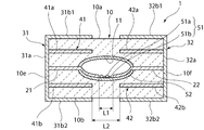
- FIG. 1 is a schematic cross-sectional view of an ESD protection apparatus according to an embodiment of the present invention.
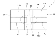
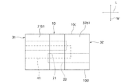
- FIG. 2 is a schematic plan view of an ESD protection apparatus according to an embodiment of the present invention.
- FIG. 3 is a schematic plan view of the ESD protection apparatus according to the first modification.
- FIG. 4 is a schematic plan view of the ESD protection apparatus according to the second modification.
- FIG. 5 is a schematic plan view of an ESD protection apparatus according to a third modification.
- FIG. 6 is a schematic plan view of an ESD protection apparatus according to a fourth modification.
- FIG. 7 is a schematic plan view of an ESD protection apparatus according to a fifth modification.
- FIG. 8 is a schematic plan view of an ESD protection apparatus according to a sixth modification.
- FIG. 1 is a schematic cross-sectional view of an ESD protection apparatus according to an embodiment of the present invention.
- FIG. 2 is a schematic plan view of an ESD protection apparatus according to an embodiment of the present invention.
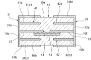
- FIG. 9 is a schematic cross-sectional view of an ESD protection apparatus according to a seventh modification.
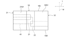
- FIG. 10 is a schematic plan view of an ESD protection apparatus according to an eighth modification.
- FIG. 11 is a schematic plan view of an ESD protection apparatus according to a ninth modification.
- FIG. 12 is a schematic plan view of an ESD protection apparatus according to a tenth modification.
- FIG. 13 is a schematic plan view of an ESD protection apparatus according to an eleventh modification.
- FIG. 1 is a schematic cross-sectional view of an ESD protection apparatus according to this embodiment.
- FIG. 2 is a schematic plan view of the ESD protection apparatus according to this embodiment.
- the ESD protection device 1 has an insulating material 10 having a cavity 11.
- the insulating material 10 is a hexahedron.
- hexahedron means a general solid having six faces. Each of the six surfaces constituting the hexahedron may be non-planar. Of the surfaces constituting the hexahedron, the opposing surfaces may be parallel to each other or non-parallel. The corners and ridges of the hexahedron may each be chamfered or have a rounded shape.
- the insulating material 10 is provided in a substantially rectangular parallelepiped shape.
- the insulating material 10 includes first and second main faces 10a and 10b parallel to each other, first and second side faces 10c and 10d parallel to each other, and first and second end faces 10e and 10f parallel to each other.
- the insulating material 10 can be composed of appropriate ceramics. Specifically, the insulating material 10 can be made of, for example, low temperature co-fired ceramics (LTCC: Low Temperature Co-fired Ceramics) containing Ba, Al, and Si as main components. Note that a resin substrate containing polyimide resin, epoxy resin, or the like may be used as the insulating material 10.
- LTCC Low Temperature Co-fired Ceramics
- the first and second discharge electrodes 21 and 22 are provided inside the insulating material 10.
- the first and second discharge electrodes 21 and 22 are provided in parallel with the first and second main surfaces 10a and 10b, respectively.
- the first discharge electrode 21 is drawn out to the first end face 10e.
- the second discharge electrode 22 is drawn out to the second end face 10f.
- the distal end portion of the first discharge electrode 21 and the distal end portion of the second discharge electrode 22 are located in the cavity 11.
- the front end portion of the first discharge electrode 21 and the front end portion of the second discharge electrode 22 are opposed to each other in the cavity 11.
- First and second external electrodes 31 and 32 are provided on the outer surface of the insulating material 10. Specifically, the first external electrode 31 is provided on at least one of the first portion 31a provided on the first end face 10e and the first and second main faces 10a, 10b. And second portions 31b1 and 31b2. However, the first external electrode may be provided only on the first end face. The first external electrode 31 is electrically connected to the first discharge electrode 21 in the first portion 31a.
- the second external electrode 32 includes a third portion 32a provided on the second end surface 10f and a fourth portion provided on at least one of the first and second main surfaces 10a and 10b. 32b1 and 32b2. However, the second external electrode may be provided only on the second end face. The second external electrode 32 is electrically connected to the second discharge electrode 22 in the third portion 32a.
- a discharge auxiliary electrode 51 is disposed between the tip portion of the first discharge electrode 21 and the tip portion of the second discharge electrode 22.
- the discharge auxiliary electrode is provided between the first and second discharge electrodes and the insulating material 10 in addition to between the tip portion of the first discharge electrode and the tip portion of the second discharge electrode. It may be.
- the discharge auxiliary electrode 51 has a function of reducing the discharge start voltage. Specifically, by providing the discharge auxiliary electrode 51, in addition to creeping discharge and air discharge, discharge via the discharge auxiliary electrode 51 also occurs. Usually, the creeping discharge, the air discharge, and the discharge through the discharge auxiliary electrode 51 have the lowest starting voltage of the discharge through the discharge auxiliary electrode 51. Therefore, by providing the discharge auxiliary electrode 51, the discharge start voltage can be lowered. Therefore, the dielectric breakdown of the ESD protection apparatus 1 can be suppressed. Moreover, the responsiveness of the ESD protection apparatus 1 can be improved by providing the discharge auxiliary electrode 51.
- the discharge auxiliary electrode 51 can be constituted by, for example, a particle dispersion in which a plurality of metal particles 51a whose surfaces are coated with an inorganic material having no conductivity and a plurality of semiconductor ceramic particles 51b are dispersed.
- the discharge auxiliary electrode 51 is formed, for example, by applying and baking a paste containing a plurality of metal particles 51a whose surfaces are coated with an inorganic material having no conductivity and a plurality of semiconductor ceramic particles 51b. be able to.
- the metal particles 51a can be made of, for example, Cu or Ni.
- the diameter of the metal particles 51a can be, for example, about 2 ⁇ m to 3 ⁇ m.
- the coating film of the metal particles 51a can be made of, for example, aluminum oxide.
- the semiconductor ceramic particles 51b include, for example, carbides such as silicon carbide, titanium carbide, zirconium carbide, molybdenum carbide or tungsten carbide, nitrides such as titanium nitride, zirconium nitride, chromium nitride, vanadium nitride or tantalum nitride, titanium silicide, silica Silicides such as zirconium silicide, tungsten silicide, molybdenum silicide, chromium silicide, boride such as titanium boride, zirconium boride, chromium boride, lanthanum boride, molybdenum boride, tungsten boride, zinc oxide, An oxide such as strontium titanate can be used.
- carbides such as silicon carbide, titanium carbide, zirconium carbide, molybdenum carbide or tungsten carbide
- nitrides such as titanium nit
- the discharge auxiliary electrode 51 may further include insulating particles made of aluminum oxide or the like in addition to the metal particles 51a and the semiconductor ceramic particles 51b.
- a protective layer 52 is provided between the insulating material 10 and at least one tip of the first and second discharge electrodes 21 and 22. Specifically, the protective layer 52 is provided so as to cover substantially the entire inner wall of the cavity 11. By providing this protective layer 52, it is possible to suppress the component contained in the insulating material 10 from reaching the tip. Therefore, it is possible to suppress a decrease in discharge characteristics due to deterioration of the first and second discharge electrodes 21 and 22 of the ESD protection apparatus 1.
- the protective layer 52 is preferably made of a ceramic having a sintering temperature higher than that of the ceramic constituting the insulating material 10.
- the protective layer 52 preferably contains at least one selected from the group consisting of alumina, mullite, zirconia, magnesia and quartz, for example.
- first and second inner conductors 41 and 42 are provided in the insulating material 10.
- the distal end portion of the first inner conductor 41 and the distal end portion of the second inner conductor 42 are opposed to each other.
- the front end portion of the first inner conductor 41 and the front end portion of the second inner conductor 42 face each other, so that the generated heat can be radiated to the first outer electrode and the second outer electrode in a balanced manner. Therefore, heat can be dissipated more efficiently.
- the distance L2 between the front end portion of the first inner conductor 41 and the front end portion of the second inner conductor 42 is between the front end portion of the first discharge electrode 21 and the front end portion of the second discharge electrode 22. It is larger than the distance L1.
- L2 is preferably 2 times or more of L1, and more preferably 3 times or more. This is because if L2 is too small, a discharge occurs between the inner conductors 41 and 42.
- the first inner conductor 41 is drawn out to the first end face 10e.
- the first inner conductor 41 is connected to the first portion 31 a of the first outer electrode 31.
- the first inner conductor 41 includes a first inner conductor 41 a located on one side in the thickness direction of the cavity 11 and a first inner conductor 41 b located on the other side in the thickness direction of the cavity 11. That is, the first inner conductors 41 a and 41 b are provided on both sides of the cavity 11 in the thickness direction.
- a plurality of first inner conductors 41a and 41b may be provided at intervals in the thickness direction.
- the second inner conductor 42 is drawn out to the second end face 10f.
- the second inner conductor 42 is connected to the third portion 32 a of the second outer electrode 32.
- the second inner conductor 42 includes a second inner conductor 42 a located on one side in the thickness direction of the cavity 11 and a second inner conductor 42 b located on the other side in the thickness direction of the cavity 11. That is, the second inner conductors 42 a and 42 b are provided on both sides of the cavity 11 in the thickness direction.
- a plurality of second inner conductors 42a and 42b may be provided at intervals in the thickness direction.
- At least one of the first and second inner conductors 41 and 42 is provided so as to overlap the cavity 11 when viewed in plan (when viewed from the thickness direction).
- the second portions 31b1 and 31b2 and the fourth portions 32b1 and 32b2 are also provided so as to overlap the cavity 11 when viewed in plan.
- the first and second discharge electrodes 21 and 22, the first and second outer electrodes 31 and 32, and the first and second inner conductors 41 and 42 are, for example, Cu, Ag, Pd, and Pt, respectively. , Al, Ni, and metals containing at least one of W (including alloys).
- the first and second discharge electrodes 21 and 22, the first and second outer electrodes 31 and 32, and the first and second inner conductors 41 and 42 are preferably made of the same material.
- the first and second inner conductors 41 and 42 having higher thermal conductivity than the insulating material 10 are provided. For this reason, the heat of the insulating material 10 is easily radiated through the first and second inner conductors 41 and 42 and the first and second outer electrodes 31 and 32. Therefore, the ESD protection apparatus 1 having improved heat dissipation can be realized.
- At least one of the first and second inner conductors 41 and 42 is provided so as to overlap the cavity 11 when viewed in plan. For this reason, the heat of the part in which the cavity 11 which is easy to generate heat is provided can be efficiently dissipated.
- the surface areas of the first and second external electrodes 31, 32 are increased by providing the first and second external electrodes 31, 32 with the second and fourth portions 31b1, 31b2, 32b1, 32b2. Can do. Therefore, heat can be dissipated more efficiently.
- the second and fourth portions 31b1, 31b2, 32b1, and 32b2 are provided so as to overlap the cavity 11 when viewed in plan. For this reason, the heat of the part provided with the cavity 11 that is likely to generate heat can be more efficiently dissipated.
- the shape of the internal conductors 41 and 42 is not limited to the shape shown in FIG.1 and FIG.2.
- inner conductors 41 and 42 in which the end face 10e, 10f side portion is narrow and the center side is wide may be provided.
- a plurality of inner conductors 41 and 42 arranged along the width direction may be provided.
- an internal conductor 41 may be provided so as to cross the cavity 11.
- the inner conductor 41 overlaps with a facing portion between the tip portion of the first discharge electrode 21 and the tip portion of the second discharge electrode 22 in plan view. Therefore, the heat of the part provided with the cavity 11 that easily generates heat can be more efficiently dissipated.
- one of the inner conductors 41 and 42 may be longer than the other.
- the internal conductors 41 and 42 may be provided so as not to overlap the cavity 11.
- the inner conductors 41 and 42 are provided at the four corners of the insulating material 10.
- the insulating material 10 may not have a cavity.
- the distal end portion of the first discharge electrode 21 and the distal end portion of the second discharge electrode 22 face each other in the extending direction of the discharge electrodes 21 and 22 (length direction L) will be described.
- the present invention is not limited to this configuration.
- the tip of the first discharge electrode 21 and the tip of the second discharge electrode 22 extend in the direction in which the discharge electrodes 21 and 22 extend (length direction L). May not face each other.
- the position in the width direction W of the tip portion of the first discharge electrode 21 is different from the position in the width direction W of the tip portion of the second discharge electrode 22.
- the position in the length direction L of the tip portion of the first discharge electrode 21 and the position in the length direction L of the tip portion of the second discharge electrode 22 are substantially the same. For this reason, the corner on one side in the width direction W of the first discharge electrode 21 and the corner on the other side in the width direction W of the second discharge electrode 22 face each other.
- the position of the tip portion of the first discharge electrode 21 in the width direction W is different from the position of the tip portion of the second discharge electrode 22 in the width direction W.
- a part of the first discharge electrode 21 and a part of the second discharge electrode 22 face each other in the width direction W.
- a part of the first discharge electrode 21 and a part of the second discharge electrode 22 face each other in the width direction W.
- the shortest distance between the portions where the first discharge electrode 21 and the second discharge electrode 22 face each other in the width direction W is between the tip of the first discharge electrode 21 and the second discharge electrode 22.
- the distance in the length direction L is shorter than each of the distance in the length direction L between the tip portion of the second discharge electrode 22 and the first discharge electrode 21. For this reason, a discharge occurs in a portion where the first discharge electrode 21 and the second discharge electrode 22 face each other in the width direction W.
- Example 1 Under the following conditions, an ESD protection device having a configuration substantially similar to that of the ESD protection device 1 according to the above embodiment was produced.
- Ceramic used for the construction of the insulating material BAS material mainly composed of Ba, Al and Si Discharge electrode, external electrode, internal conductor: Cu
- Dimensions of ESD protection device length 1.0mm x width 0.5mm x thickness 0.3mm
- Planar shape of the cavity rectangular shape
- Length of the cavity 200 ⁇ m
- L2 100 ⁇ m
- Second and fourth parts of first and second external electrodes None
- Example 2 The ESD protection device is provided in the same manner as in Example 1 except that the second and fourth portions of the first and second external electrodes are respectively provided with the same length as the first or second internal conductor. Produced.
- Example 3 An ESD protection device was fabricated in the same manner as in Example 1 except that the distance L2 was 500 ⁇ m so that each of the first and second inner conductors did not overlap the cavity.
- Example 4 The distance L2 is set to 500 ⁇ m so that each of the first and second inner conductors does not overlap the cavity, and the length of the second and fourth portions is the same as that of the first or second inner conductor. Produced an ESD protection device in the same manner as in Example 2.
- Example 5 As shown in FIG. 5, an ESD protection device was produced in the same manner as in Example 1 except that an internal conductor crossing the cavity was formed.
- Example 6 As shown in FIG. 5, an ESD protection device was produced in the same manner as in Example 2 except that an inner conductor that crossed the cavity was formed and a second portion similar to the inner conductor was provided.
- ESD repeated resistance evaluation Application of 8 kV by contact discharge was performed for the number of times shown in Table 1, and then the discharge response to ESD was evaluated.
- the discharge response to ESD was performed by an electrostatic discharge immunity test defined in IEC standard, IEC61000-4-2. It was investigated whether or not discharge occurred between the discharge electrodes of the sample by applying 8 kV by contact discharge.
- the peak voltage detected on the protection circuit side exceeds 700V, the ESD repeatability is poor (x mark), when the peak voltage is 600-700V ( ⁇ mark), and when the peak voltage is 450-600V ESD repeat
- a sample having good resistance ( ⁇ mark) and a peak voltage of less than 450 V was determined to have particularly good ESD repeat resistance (marked with ⁇ ).
Landscapes
- Thermistors And Varistors (AREA)
Priority Applications (3)
| Application Number | Priority Date | Filing Date | Title |
|---|---|---|---|
| JP2014507613A JP5796677B2 (ja) | 2012-03-28 | 2013-03-08 | Esd保護装置 |
| CN201390000358.3U CN204376195U (zh) | 2012-03-28 | 2013-03-08 | Esd保护装置 |
| US14/484,357 US9516728B2 (en) | 2012-03-28 | 2014-09-12 | ESD protection device |
Applications Claiming Priority (2)
| Application Number | Priority Date | Filing Date | Title |
|---|---|---|---|
| JP2012074220 | 2012-03-28 | ||
| JP2012-074220 | 2012-03-28 |
Related Child Applications (1)
| Application Number | Title | Priority Date | Filing Date |
|---|---|---|---|
| US14/484,357 Continuation US9516728B2 (en) | 2012-03-28 | 2014-09-12 | ESD protection device |
Publications (1)
| Publication Number | Publication Date |
|---|---|
| WO2013146189A1 true WO2013146189A1 (fr) | 2013-10-03 |
Family
ID=49259457
Family Applications (1)
| Application Number | Title | Priority Date | Filing Date |
|---|---|---|---|
| PCT/JP2013/056466 Ceased WO2013146189A1 (fr) | 2012-03-28 | 2013-03-08 | Dispositif de protection contre les décharges électrostatiques (esd) |
Country Status (4)
| Country | Link |
|---|---|
| US (1) | US9516728B2 (fr) |
| JP (1) | JP5796677B2 (fr) |
| CN (1) | CN204376195U (fr) |
| WO (1) | WO2013146189A1 (fr) |
Cited By (1)
| Publication number | Priority date | Publication date | Assignee | Title |
|---|---|---|---|---|
| JP2015138932A (ja) * | 2014-01-24 | 2015-07-30 | Tdk株式会社 | 静電気保護部品 |
Families Citing this family (4)
| Publication number | Priority date | Publication date | Assignee | Title |
|---|---|---|---|---|
| DE102016108604B4 (de) * | 2016-05-10 | 2025-08-07 | Tdk Electronics Ag | Vielschichtbauelement und Verfahren zur Herstellung eines Vielschichtbauelements |
| CN109891680B (zh) * | 2016-11-04 | 2021-11-16 | 阿莫技术有限公司 | 功能性接触器 |
| JP7575352B2 (ja) * | 2021-06-03 | 2024-10-29 | Tdk株式会社 | 過渡電圧保護デバイス |
| JP2024033860A (ja) * | 2022-08-31 | 2024-03-13 | Tdk株式会社 | 過渡電圧保護デバイス |
Citations (6)
| Publication number | Priority date | Publication date | Assignee | Title |
|---|---|---|---|---|
| JPS6379087U (fr) * | 1986-11-11 | 1988-05-25 | ||
| JPH09223566A (ja) * | 1996-02-16 | 1997-08-26 | Hightech Syst:Kk | サージ吸収素子 |
| JP2000243534A (ja) * | 1999-02-17 | 2000-09-08 | Mitsubishi Materials Corp | チップ型サージアブソーバ及びその製造方法 |
| WO2010061550A1 (fr) * | 2008-11-26 | 2010-06-03 | 株式会社 村田製作所 | Dispositif de protection contre les décharges électrostatiques et son procédé de fabrication |
| JP2010146779A (ja) * | 2008-12-17 | 2010-07-01 | Panasonic Corp | 過電圧保護部品 |
| JP2011187439A (ja) * | 2010-02-15 | 2011-09-22 | Murata Mfg Co Ltd | Esd保護装置 |
Family Cites Families (3)
| Publication number | Priority date | Publication date | Assignee | Title |
|---|---|---|---|---|
| CN101542856B (zh) | 2007-05-28 | 2012-05-30 | 株式会社村田制作所 | 静电放电保护装置 |
| JP5505564B2 (ja) * | 2011-08-31 | 2014-05-28 | 株式会社村田製作所 | 積層型コモンモードチョークコイルおよび高周波部品 |
| CN103797669B (zh) * | 2011-09-14 | 2016-08-17 | 株式会社村田制作所 | Esd保护器件及其制造方法 |
-
2013
- 2013-03-08 CN CN201390000358.3U patent/CN204376195U/zh not_active Expired - Lifetime
- 2013-03-08 WO PCT/JP2013/056466 patent/WO2013146189A1/fr not_active Ceased
- 2013-03-08 JP JP2014507613A patent/JP5796677B2/ja active Active
-
2014
- 2014-09-12 US US14/484,357 patent/US9516728B2/en active Active
Patent Citations (6)
| Publication number | Priority date | Publication date | Assignee | Title |
|---|---|---|---|---|
| JPS6379087U (fr) * | 1986-11-11 | 1988-05-25 | ||
| JPH09223566A (ja) * | 1996-02-16 | 1997-08-26 | Hightech Syst:Kk | サージ吸収素子 |
| JP2000243534A (ja) * | 1999-02-17 | 2000-09-08 | Mitsubishi Materials Corp | チップ型サージアブソーバ及びその製造方法 |
| WO2010061550A1 (fr) * | 2008-11-26 | 2010-06-03 | 株式会社 村田製作所 | Dispositif de protection contre les décharges électrostatiques et son procédé de fabrication |
| JP2010146779A (ja) * | 2008-12-17 | 2010-07-01 | Panasonic Corp | 過電圧保護部品 |
| JP2011187439A (ja) * | 2010-02-15 | 2011-09-22 | Murata Mfg Co Ltd | Esd保護装置 |
Cited By (1)
| Publication number | Priority date | Publication date | Assignee | Title |
|---|---|---|---|---|
| JP2015138932A (ja) * | 2014-01-24 | 2015-07-30 | Tdk株式会社 | 静電気保護部品 |
Also Published As
| Publication number | Publication date |
|---|---|
| US9516728B2 (en) | 2016-12-06 |
| US20140376147A1 (en) | 2014-12-25 |
| JPWO2013146189A1 (ja) | 2015-12-10 |
| CN204376195U (zh) | 2015-06-03 |
| JP5796677B2 (ja) | 2015-10-21 |
Similar Documents
| Publication | Publication Date | Title |
|---|---|---|
| US8711537B2 (en) | ESD protection device and method for producing the same | |
| JP4434314B2 (ja) | Esd保護デバイス | |
| JP5796677B2 (ja) | Esd保護装置 | |
| WO2013065672A1 (fr) | Dispositif de protection contre les décharges électrostatiques | |
| JP5954447B2 (ja) | Esd保護装置 | |
| JP5874743B2 (ja) | Esd保護装置 | |
| JP5971413B2 (ja) | Esd保護装置 | |
| JP5725262B2 (ja) | Esd保護装置 | |
| JP2024033860A (ja) | 過渡電圧保護デバイス | |
| JP6036989B2 (ja) | Esd保護装置 | |
| JP6086151B2 (ja) | Esd保護装置 | |
| JP2023041202A (ja) | 過渡電圧保護デバイス | |
| JP5757294B2 (ja) | Esd保護装置及びその製造方法 | |
| JP2023042847A (ja) | 過渡電圧保護デバイス | |
| JP7322925B2 (ja) | 過渡電圧保護デバイス | |
| US9413168B2 (en) | ESD protection device | |
| JP7593888B2 (ja) | 過渡電圧保護デバイス | |
| JP2024033857A (ja) | 過渡電圧保護デバイス | |
| JP2023005443A (ja) | 過渡電圧保護デバイス | |
| CN115441307A (zh) | 瞬态电压保护器件 | |
| WO2013146324A1 (fr) | Dispositif de protection contre les décharges électrostatiques et procédé de production associé |
Legal Events
| Date | Code | Title | Description |
|---|---|---|---|
| WWE | Wipo information: entry into national phase |
Ref document number: 201390000358.3 Country of ref document: CN |
|
| 121 | Ep: the epo has been informed by wipo that ep was designated in this application |
Ref document number: 13769809 Country of ref document: EP Kind code of ref document: A1 |
|
| ENP | Entry into the national phase |
Ref document number: 2014507613 Country of ref document: JP Kind code of ref document: A |
|
| NENP | Non-entry into the national phase |
Ref country code: DE |
|
| 122 | Ep: pct application non-entry in european phase |
Ref document number: 13769809 Country of ref document: EP Kind code of ref document: A1 |