WO2013146338A1 - スイッチング電源装置 - Google Patents
スイッチング電源装置 Download PDFInfo
- Publication number
- WO2013146338A1 WO2013146338A1 PCT/JP2013/057371 JP2013057371W WO2013146338A1 WO 2013146338 A1 WO2013146338 A1 WO 2013146338A1 JP 2013057371 W JP2013057371 W JP 2013057371W WO 2013146338 A1 WO2013146338 A1 WO 2013146338A1
- Authority
- WO
- WIPO (PCT)
- Prior art keywords
- winding
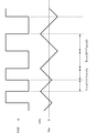
- switching element
- low
- voltage
- side switching
- Prior art date
- Legal status (The legal status is an assumption and is not a legal conclusion. Google has not performed a legal analysis and makes no representation as to the accuracy of the status listed.)
- Ceased
Links
Images





Classifications
-
- H—ELECTRICITY
- H02—GENERATION; CONVERSION OR DISTRIBUTION OF ELECTRIC POWER
- H02M—APPARATUS FOR CONVERSION BETWEEN AC AND AC, BETWEEN AC AND DC, OR BETWEEN DC AND DC, AND FOR USE WITH MAINS OR SIMILAR POWER SUPPLY SYSTEMS; CONVERSION OF DC OR AC INPUT POWER INTO SURGE OUTPUT POWER; CONTROL OR REGULATION THEREOF
- H02M3/00—Conversion of DC power input into DC power output
- H02M3/22—Conversion of DC power input into DC power output with intermediate conversion into AC
- H02M3/24—Conversion of DC power input into DC power output with intermediate conversion into AC by static converters
- H02M3/28—Conversion of DC power input into DC power output with intermediate conversion into AC by static converters using discharge tubes with control electrode or semiconductor devices with control electrode to produce the intermediate AC
- H02M3/325—Conversion of DC power input into DC power output with intermediate conversion into AC by static converters using discharge tubes with control electrode or semiconductor devices with control electrode to produce the intermediate AC using devices of a triode or a transistor type requiring continuous application of a control signal
- H02M3/335—Conversion of DC power input into DC power output with intermediate conversion into AC by static converters using discharge tubes with control electrode or semiconductor devices with control electrode to produce the intermediate AC using devices of a triode or a transistor type requiring continuous application of a control signal using semiconductor devices only
- H02M3/3353—Conversion of DC power input into DC power output with intermediate conversion into AC by static converters using discharge tubes with control electrode or semiconductor devices with control electrode to produce the intermediate AC using devices of a triode or a transistor type requiring continuous application of a control signal using semiconductor devices only having at least two simultaneously operating switches on the input side, e.g. "double forward" or "double (switched) flyback" converter
-
- H—ELECTRICITY
- H01—ELECTRIC ELEMENTS
- H01F—MAGNETS; INDUCTANCES; TRANSFORMERS; SELECTION OF MATERIALS FOR THEIR MAGNETIC PROPERTIES
- H01F27/00—Details of transformers or inductances, in general
- H01F27/28—Coils; Windings; Conductive connections
-
- H—ELECTRICITY
- H01—ELECTRIC ELEMENTS
- H01F—MAGNETS; INDUCTANCES; TRANSFORMERS; SELECTION OF MATERIALS FOR THEIR MAGNETIC PROPERTIES
- H01F27/00—Details of transformers or inductances, in general
- H01F27/28—Coils; Windings; Conductive connections
- H01F27/32—Insulating of coils, windings, or parts thereof
- H01F27/324—Insulation between coil and core, between different winding sections, around the coil; Other insulation structures
- H01F27/325—Coil bobbins
-
- H—ELECTRICITY
- H01—ELECTRIC ELEMENTS
- H01F—MAGNETS; INDUCTANCES; TRANSFORMERS; SELECTION OF MATERIALS FOR THEIR MAGNETIC PROPERTIES
- H01F38/00—Adaptations of transformers or inductances for specific applications or functions
- H01F38/02—Adaptations of transformers or inductances for specific applications or functions for non-linear operation
- H01F38/06—Adaptations of transformers or inductances for specific applications or functions for non-linear operation for changing the wave shape
-
- H—ELECTRICITY
- H02—GENERATION; CONVERSION OR DISTRIBUTION OF ELECTRIC POWER
- H02M—APPARATUS FOR CONVERSION BETWEEN AC AND AC, BETWEEN AC AND DC, OR BETWEEN DC AND DC, AND FOR USE WITH MAINS OR SIMILAR POWER SUPPLY SYSTEMS; CONVERSION OF DC OR AC INPUT POWER INTO SURGE OUTPUT POWER; CONTROL OR REGULATION THEREOF
- H02M3/00—Conversion of DC power input into DC power output
- H02M3/01—Resonant DC/DC converters
-
- H—ELECTRICITY
- H02—GENERATION; CONVERSION OR DISTRIBUTION OF ELECTRIC POWER
- H02M—APPARATUS FOR CONVERSION BETWEEN AC AND AC, BETWEEN AC AND DC, OR BETWEEN DC AND DC, AND FOR USE WITH MAINS OR SIMILAR POWER SUPPLY SYSTEMS; CONVERSION OF DC OR AC INPUT POWER INTO SURGE OUTPUT POWER; CONTROL OR REGULATION THEREOF
- H02M3/00—Conversion of DC power input into DC power output
- H02M3/22—Conversion of DC power input into DC power output with intermediate conversion into AC
- H02M3/24—Conversion of DC power input into DC power output with intermediate conversion into AC by static converters
- H02M3/28—Conversion of DC power input into DC power output with intermediate conversion into AC by static converters using discharge tubes with control electrode or semiconductor devices with control electrode to produce the intermediate AC
- H02M3/325—Conversion of DC power input into DC power output with intermediate conversion into AC by static converters using discharge tubes with control electrode or semiconductor devices with control electrode to produce the intermediate AC using devices of a triode or a transistor type requiring continuous application of a control signal
- H02M3/335—Conversion of DC power input into DC power output with intermediate conversion into AC by static converters using discharge tubes with control electrode or semiconductor devices with control electrode to produce the intermediate AC using devices of a triode or a transistor type requiring continuous application of a control signal using semiconductor devices only
- H02M3/33507—Conversion of DC power input into DC power output with intermediate conversion into AC by static converters using discharge tubes with control electrode or semiconductor devices with control electrode to produce the intermediate AC using devices of a triode or a transistor type requiring continuous application of a control signal using semiconductor devices only with automatic control of the output voltage or current, e.g. flyback converters
- H02M3/33523—Conversion of DC power input into DC power output with intermediate conversion into AC by static converters using discharge tubes with control electrode or semiconductor devices with control electrode to produce the intermediate AC using devices of a triode or a transistor type requiring continuous application of a control signal using semiconductor devices only with automatic control of the output voltage or current, e.g. flyback converters with galvanic isolation between input and output of both the power stage and the feedback loop
-
- H—ELECTRICITY
- H02—GENERATION; CONVERSION OR DISTRIBUTION OF ELECTRIC POWER
- H02M—APPARATUS FOR CONVERSION BETWEEN AC AND AC, BETWEEN AC AND DC, OR BETWEEN DC AND DC, AND FOR USE WITH MAINS OR SIMILAR POWER SUPPLY SYSTEMS; CONVERSION OF DC OR AC INPUT POWER INTO SURGE OUTPUT POWER; CONTROL OR REGULATION THEREOF
- H02M3/00—Conversion of DC power input into DC power output
- H02M3/22—Conversion of DC power input into DC power output with intermediate conversion into AC
- H02M3/24—Conversion of DC power input into DC power output with intermediate conversion into AC by static converters
- H02M3/28—Conversion of DC power input into DC power output with intermediate conversion into AC by static converters using discharge tubes with control electrode or semiconductor devices with control electrode to produce the intermediate AC
- H02M3/325—Conversion of DC power input into DC power output with intermediate conversion into AC by static converters using discharge tubes with control electrode or semiconductor devices with control electrode to produce the intermediate AC using devices of a triode or a transistor type requiring continuous application of a control signal
- H02M3/335—Conversion of DC power input into DC power output with intermediate conversion into AC by static converters using discharge tubes with control electrode or semiconductor devices with control electrode to produce the intermediate AC using devices of a triode or a transistor type requiring continuous application of a control signal using semiconductor devices only
- H02M3/33538—Conversion of DC power input into DC power output with intermediate conversion into AC by static converters using discharge tubes with control electrode or semiconductor devices with control electrode to produce the intermediate AC using devices of a triode or a transistor type requiring continuous application of a control signal using semiconductor devices only of the forward type
- H02M3/33546—Conversion of DC power input into DC power output with intermediate conversion into AC by static converters using discharge tubes with control electrode or semiconductor devices with control electrode to produce the intermediate AC using devices of a triode or a transistor type requiring continuous application of a control signal using semiconductor devices only of the forward type with automatic control of the output voltage or current
-
- H—ELECTRICITY
- H02—GENERATION; CONVERSION OR DISTRIBUTION OF ELECTRIC POWER
- H02M—APPARATUS FOR CONVERSION BETWEEN AC AND AC, BETWEEN AC AND DC, OR BETWEEN DC AND DC, AND FOR USE WITH MAINS OR SIMILAR POWER SUPPLY SYSTEMS; CONVERSION OF DC OR AC INPUT POWER INTO SURGE OUTPUT POWER; CONTROL OR REGULATION THEREOF
- H02M3/00—Conversion of DC power input into DC power output
- H02M3/22—Conversion of DC power input into DC power output with intermediate conversion into AC
- H02M3/24—Conversion of DC power input into DC power output with intermediate conversion into AC by static converters
- H02M3/28—Conversion of DC power input into DC power output with intermediate conversion into AC by static converters using discharge tubes with control electrode or semiconductor devices with control electrode to produce the intermediate AC
- H02M3/325—Conversion of DC power input into DC power output with intermediate conversion into AC by static converters using discharge tubes with control electrode or semiconductor devices with control electrode to produce the intermediate AC using devices of a triode or a transistor type requiring continuous application of a control signal
- H02M3/335—Conversion of DC power input into DC power output with intermediate conversion into AC by static converters using discharge tubes with control electrode or semiconductor devices with control electrode to produce the intermediate AC using devices of a triode or a transistor type requiring continuous application of a control signal using semiconductor devices only
- H02M3/33569—Conversion of DC power input into DC power output with intermediate conversion into AC by static converters using discharge tubes with control electrode or semiconductor devices with control electrode to produce the intermediate AC using devices of a triode or a transistor type requiring continuous application of a control signal using semiconductor devices only having several active switching elements
- H02M3/33571—Half-bridge at primary side of an isolation transformer
-
- H—ELECTRICITY
- H02—GENERATION; CONVERSION OR DISTRIBUTION OF ELECTRIC POWER
- H02M—APPARATUS FOR CONVERSION BETWEEN AC AND AC, BETWEEN AC AND DC, OR BETWEEN DC AND DC, AND FOR USE WITH MAINS OR SIMILAR POWER SUPPLY SYSTEMS; CONVERSION OF DC OR AC INPUT POWER INTO SURGE OUTPUT POWER; CONTROL OR REGULATION THEREOF
- H02M1/00—Details of apparatus for conversion
- H02M1/0048—Circuits or arrangements for reducing losses
- H02M1/0054—Transistor switching losses
- H02M1/0058—Transistor switching losses by employing soft switching techniques, i.e. commutation of transistors when applied voltage is zero or when current flow is zero
-
- Y—GENERAL TAGGING OF NEW TECHNOLOGICAL DEVELOPMENTS; GENERAL TAGGING OF CROSS-SECTIONAL TECHNOLOGIES SPANNING OVER SEVERAL SECTIONS OF THE IPC; TECHNICAL SUBJECTS COVERED BY FORMER USPC CROSS-REFERENCE ART COLLECTIONS [XRACs] AND DIGESTS
- Y02—TECHNOLOGIES OR APPLICATIONS FOR MITIGATION OR ADAPTATION AGAINST CLIMATE CHANGE
- Y02B—CLIMATE CHANGE MITIGATION TECHNOLOGIES RELATED TO BUILDINGS, e.g. HOUSING, HOUSE APPLIANCES OR RELATED END-USER APPLICATIONS
- Y02B70/00—Technologies for an efficient end-user side electric power management and consumption
- Y02B70/10—Technologies improving the efficiency by using switched-mode power supplies [SMPS], i.e. efficient power electronics conversion e.g. power factor correction or reduction of losses in power supplies or efficient standby modes
Definitions
- the present invention relates to a switching power supply device, and more particularly to a resonant switching power supply device that uses a resonance phenomenon for power conversion operation.
- the switching power supply device described in Patent Document 1 turns on and off the high-side switching element and the low-side switching element alternately based on the voltage generated in two auxiliary windings provided in the insulation transformer, and the primary winding of the insulation transformer. A resonant voltage is generated on the line, and as a result, a constant DC voltage is output from the secondary winding of the isolation transformer.
- the switching power supply device described in Patent Document 1 has a configuration in which a primary winding is wound between two auxiliary windings and a secondary winding. As a result, the two auxiliary windings generate a voltage generated in the two auxiliary windings in the primary winding by strengthening the coupling with the primary winding and weakening the coupling with the secondary winding. This makes it possible to perform ZVS (zero voltage switching) operation.
- the low-side switching element is driven with a waveform similar to the voltage waveform generated in the inductance of the primary winding, and the high-side switching element is generated in the inductance of the secondary winding. It is desirable to drive with a waveform similar to the voltage waveform, and the operation in which the high-side switching element and the low-side switching element are alternately turned on / off becomes more reliable.
- the low-side drive winding strengthens the coupling with the primary winding
- the voltage waveforms of the low-side drive winding and the primary winding are similar
- the high-side drive winding has a coupling with the secondary winding. It is necessary to make the voltage waveforms of the high-side drive winding and the secondary winding similar to each other.
- an object of the present invention is to provide a switching power supply device in which an appropriate distance is provided between the windings.
- the coupling between the low side drive winding and the primary winding and the coupling between the high side drive winding and the secondary winding are strengthened, and the ZVS operation of the high side switching element and the low side switching element can be performed reliably. It is to provide a power supply device.
- a switching power supply includes a power supply voltage input unit to which an input power supply voltage is input, a DC voltage output unit to which a DC voltage is output, a primary winding wound around a bobbin winding unit, and 2 A secondary winding, a low-side drive winding and a high-side drive winding, a transformer having a core forming a closed magnetic circuit, a capacitor including the primary winding to form an LC resonance circuit, and the power supply voltage input unit
- a switching control having a series circuit of a low-side switching element and a high-side switching element, a low-side switching control unit that controls the low-side switching element, and a high-side switching control unit that controls the high-side switching element, connected to
- the LC resonant circuit includes a leakage current of the primary winding or the secondary winding of the transformer.
- the low-side switching element is connected in series to the primary winding and applies the voltage of the power supply voltage input unit to the primary winding when turned on, and the low-side switching control unit includes the low-side drive
- the low side switching element is turned on by detecting polarity reversal of the winding voltage generated in the winding, and the low side switching element is turned off in a time based on a feedback signal of a circuit for detecting an output voltage
- the high side switching control unit Detects the polarity reversal of the winding voltage generated in the high-side drive winding, turns on the high-side switching element, turns off the high-side switching element according to the on-time of the low-side switching element
- the bobbin includes a partition having a slit, and the partition Is provided along the outer periphery of the winding part, and a first winding area in which the primary winding is wound around the winding part and a second winding area in which the secondary winding is wound.
- the primary winding is wound from the outer peripheral surface of the winding portion to a first height h1, and the secondary winding is a second height from the outer peripheral surface of the winding portion.
- the low-side drive winding and the high-side drive winding are provided along the winding axis direction with the high-side drive winding on the secondary winding side, and the primary side It is wound around a winding.
- the low-side drive winding and the high-side drive winding are wound outside the primary winding, the coupling between the low-side drive winding and the high-side drive winding and the primary winding is strong.
- the waveform of the voltage generated in the low-side drive winding is similar to the waveform of the voltage generated in the primary winding, so the low-side switching control unit detects the reversal of the voltage polarity generated in the low-side drive winding.
- the ZVS operation of the low side switching element can be reliably performed by appropriately detecting the resonance timing and turning on the low side switching element.
- the timing of resonance can be detected appropriately, the reliability of the apparatus can be improved by preventing a state in which the resonance condition is removed (“resonance out of resonance”).
- the high-side drive winding and the secondary winding have substantially the same winding axis, and at least part of the winding is wound at the same height between the heights h1 and h2.
- the coupling between the drive winding and the secondary winding is strong.
- the waveform of the voltage generated in the high-side drive winding is similar to the waveform of the voltage generated in the secondary winding, and the high-side switching control unit performs high-side switching at the timing when the voltage is generated in the secondary winding.
- the device can be turned on to perform the ZVS operation of the high-side switching device.
- the switching power supply device includes a cover that has a projection that fits into the slit of the bobbin, and covers the primary winding, the secondary winding, the low-side driving winding, and the high-side driving winding.
- the configuration is preferable.
- the convex distance is fitted to the slit of the bobbin, so that the spatial distance between the primary winding and the secondary winding can be increased to the same level as the creepage distance. While maintaining, the primary winding and the secondary winding can be brought close to each other to strengthen the mutual coupling.
- the height of the partition on the side facing the substrate on which the transformer is mounted may be higher than the second height h2.
- the convex part of the cover that covers the winding is fitted with the slit of the bobbin, so that the clearance is increased to the same level as the creepage distance to ensure a safety standard distance
- the convex part of the cover and the slit of the bobbin cannot be fitted, so in this configuration, the transformer is mounted without increasing the overall size of the transformer.
- a space insulation distance between the primary winding and the secondary winding can be ensured by making the height of the partitioning portion on the side facing the substrate higher than the second height h2.
- the partition part may be provided at a position off the center of the length of the winding part along the winding axis.
- the gap position of the core of the transformer by setting the gap position of the core of the transformer to be approximately the center of the winding portion, the leakage magnetic flux from the gap can be absorbed (shielded) by the winding, and thus the influence of the magnetic flux on the peripheral circuit can be prevented.
- the secondary winding may have a first winding and a second winding wound by a center tap and bifilar wound.
- the first winding of the primary winding and the secondary winding are made the same by coupling the primary winding with the first winding and the second winding of the secondary winding.
- the coupling between the line and the second winding can be made uniform, and an unbalanced operation at the time of center tap rectification can be prevented.
- the cross section of the core in the direction orthogonal to the winding axis may have a flat shape in which the mounting height dimension direction of the transformer is the shortest length.
- the capacitor may be connected between the high-side switching element and the low-side switching element.
- a current detection capacitor is connected in parallel to the resonance capacitor, and the current flowing through the resonance capacitor is slightly shunted to the current detection capacitor, so that the resonance current flowing through the resonance capacitor can be detected equivalently.
- an overcurrent protection circuit can be configured, and loss at the detection resistor can be reduced.
- Sectional drawing of the bobbin of the transformer according to Embodiment 1 Three views of the transformer according to the first embodiment Sectional view taken along line III-III in FIG. Three views of transformer cover Sectional view taken along line VV in FIG.
- Top view and front view of magnetic core of transformer Sectional drawing which expanded the part of a slit and a convex part at the time of covering a bobbin 1 is a circuit diagram of a switching power supply device 101 according to a first embodiment.
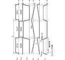
- Waveform diagram showing changes in high-side drive winding voltage and transistor base-emitter voltage when load changes occur The gate-source voltage of the low-side switching element, the gate-source voltage of the high-side switching element, the drain-source voltage of the low-side switching element, the base-emitter voltage of the transistor, the voltage Vis of the IS terminal of the switching control IC, and Waveform diagram showing the relationship of the voltage Vzt at the ZT terminal Waveform diagram of the voltage of the primary winding of the transformer T and the drain current of the low-side switching element in the state of resonance prevention Waveform diagram of the voltage of the primary winding np of the transformer T and the drain current of the low-side switching element in a state where “resonance failure” has occurred Circuit diagram of switching power supply apparatus according to Embodiment 2 Circuit diagram of switching power supply apparatus according to Embodiment 3 Circuit diagram of switching power supply apparatus according to Embodiment 4 Circuit diagram of switching power supply apparatus according to Embodiment 5 Circuit diagram of switching power supply apparatus according to Embodiment 6
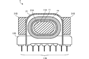
- FIG. 1 is a cross-sectional view of a bobbin of a transformer according to the first embodiment.
- FIG. 2 is a three-side view of the transformer according to the first embodiment.
- 3 is a cross-sectional view taken along line III-III in FIG.
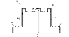
- FIG. 4 is a three-side view of the cover of the transformer.
- FIG. 5 is a cross-sectional view taken along line VV in FIG.
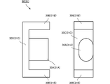
- FIG. 6 is a top view and a right side view of the magnetic core of the transformer.
- the transformer T includes a bobbin 10, a cover 20, and magnetic cores 30 and 31.
- the bobbin 10 is wound with a primary winding np, a secondary winding ns, and drive windings nb1 and nb2.
- the cover 20 covers the bobbin 10 around which the primary winding np is wound.
- the magnetic cores 30 and 31 are so-called E-type cores, which are fitted into the bobbin 10 covered with the cover 20 to form a closed magnetic path for the magnetic field of the primary winding np and the secondary winding ns.
- the bobbin 10 includes a cylindrical portion (winding portion of the present invention) 11 made of an insulating resin.
- the cylindrical portion 11 is formed along the axial direction (left and right direction in FIG. 1), and has an internal space 11A that is open at both ends.
- Center legs 30A and 31A (see FIG. 6) of magnetic cores 30 and 31, which will be described later, are inserted into the internal space 11A from openings at both ends.
- the front ends of the center legs 30A and 31A are opposed to each other through a gap (gap) at the substantially axial center of the cylindrical portion 11.
- terminal blocks 16A and 16B are provided at both axial ends of the cylindrical portion 11.
- Bobbin terminals 17A and 17B in which a plurality of pins are arranged at a predetermined pitch are provided below the terminal blocks 16A and 16B (the lower side in the drawing of FIG. 1).
- the transformer T is mounted by soldering the bobbin terminals 17A and 17B to the mounting board.
- End plates 12 ⁇ / b> A and 12 ⁇ / b> B are provided substantially perpendicular to the peripheral surface on the peripheral surface of both ends of the cylindrical portion 11.
- partition plates (partition portions of the present invention) 13 and 14 are provided substantially perpendicular to the peripheral surface on the peripheral surface at a position deviated from the approximate center in the axial direction of the cylindrical portion 11. Specifically, when the distance between the partition plate 13 and the end plate 12A is represented by L1, and the distance between the partition plate 14 and the end plate 12B is represented by L2, the relationship of L1> L2 is established.
- a slit 15 is formed between the partition plates 13 and 14.
- the slit 15 is for satisfying a safety standard distance between the primary winding np and the secondary winding ns wound around the cylindrical portion 11.
- the space between the end plate 12A and the partition plate 13 is referred to as a first section (the first winding region of the present invention), and the space between the end plate 12B and the partition plate 14 is a second section (the book).
- the second winding region of the invention is for satisfying a safety standard distance between the primary winding np and the secondary winding ns wound around the cylindrical portion 11.
- the end plates 12A and 12B and the partition plates 13 and 14 forming the first section and the second section are provided along the circumferential direction of the cylindrical portion 11, and have different heights depending on the positions in the circumferential direction. .
- the side facing the substrate that is, the side where the bobbin terminals 17A and 17B are provided is the lower side of the transformer T.
- the height h4 of the lower end plates 12A and 12B and the partition plates 13 and 14 of the transformer T is equal to the height of the upper end plates 12A and 12B and the partition plates 13 and 14 of the transformer T (this embodiment). In the form, it is higher than the height h2).
- the primary winding np is wound around the cylindrical portion 11 with the axial direction of the cylindrical portion 11 as the winding axis.
- the primary winding np is wound from the peripheral surface of the cylindrical portion 11 to a height h1.
- the secondary winding ns is wound around the cylindrical portion 11 with the axial direction of the cylindrical portion 11 as the winding axis.
- the secondary winding ns is wound from the peripheral surface of the cylindrical portion 11 to a height h2 (> h1).
- the secondary winding ns has a center tap, and two windings divided by the center tap are bifilar wound.
- partition plates 13 and 14 and a slit 15 are provided between the primary winding np and the secondary winding ns. Therefore, the creepage distance between the primary winding np and the secondary winding ns can be obtained without increasing the linear distance between the primary winding np and the secondary winding ns. As a result, a safety standard distance can be secured without weakening the magnetic coupling between the primary winding np and the secondary winding ns.
- the gap between the magnetic cores 30 and 31 is located at the approximate center of the cylindrical portion 11 in the axial direction. Therefore, the gap is located in the winding range of the primary winding np from the relationship of L1> L2. Thereby, the leakage magnetic flux generated from the gap between the magnetic cores 30 and 31 forming the closed magnetic path is absorbed (shielded) by the primary winding np, and the influence on the peripheral circuit can be reduced.
- the drive windings nb1 and nb2 are wound around the primary winding np wound around the first section.
- the drive windings nb1 and nb2 are wound side by side along the axial direction of the cylindrical portion 11 so that the drive winding nb2 is on the secondary winding ns side.
- the drive windings nb1 and nb2 are wound from the primary winding np to the height h3.
- the drive windings nb1 and nb2 are wound around the first section, the coupling with the primary winding np is strong. Further, since the drive winding nb2 is close to the secondary winding ns in the axial direction and has substantially the same height, the coil sectional area of the driving winding nb2 is equal to the coil sectional area of the secondary winding.
- the voltage waveform induced in the drive winding nb2 is similar to the voltage waveform generated in the secondary winding ns.
- the drive winding nb2 and the secondary winding ns have the same height between the heights h1 and h2. Since the winding is wound, the voltage waveform induced in the drive winding nb2 is substantially similar to the voltage waveform generated in the secondary winding ns. Even when the drive winding nb2 is wound at a height less than h3, the drive winding nb2 is wound in the region of the height of the secondary winding ns. The voltage waveform induced in nb2 and the voltage waveform generated in the secondary winding ns are almost similar.
- the height of the lower end plates 12A and 12B and the partition plates 13 and 14 of the transformer T is higher than the height of the upper end plates 12A and 12B and the partition plates 13 and 14 of the transformer T.
- the heights of the upper end plates 12A and 12B and the partition plates 13 and 14 of the transformer T are the height h2 of the secondary winding ns. Accordingly, it is possible to secure a space insulation distance between the primary winding np, the secondary winding ns and the drive windings nb1 and nb2 and the substrate on which the transformer T is mounted, while reducing the height.
- the cross section of the cylindrical portion 11 in the direction orthogonal to the axial direction has a flat shape in which the vertical direction of the transformer T (the mounting height dimension direction of the present invention) is short. Thereby, the low profile of the transformer T is realized.
- the cover 20 is made of an insulating resin and covers the bobbin 10 having the above-described configuration. As shown in FIG. 4, the cover 20 includes a central cover 21 that covers the first section and the second section of the bobbin 10.
- the center cover 21 has a side surface and an upper surface, and surrounds the first section and the second section portion of the bobbin 10 from three directions.
- the center cover 21 has openings 21 ⁇ / b> A and 21 ⁇ / b> A.
- the openings 21 ⁇ / b> A and 21 ⁇ / b> A overlap with the opening of the internal space 11 ⁇ / b> A of the cylindrical portion 11.
- the center legs 30A and 31A of the magnetic cores 30 and 31 are inserted into the internal space 11A of the cylindrical portion 11 through the openings 21A and 21A.
- an opening 21B is formed at a position facing the first section of the bobbin 10
- an opening 21C is formed at a position facing the second section of the bobbin 10.
- FIG. 7 is an enlarged cross-sectional view of the slit 15 and the convex portion 24 when the bobbin 10 is covered with the cover 20.
- the drive winding nb1 is omitted.
- the spatial distance between the primary winding np and the secondary winding ns is the same as the creepage distance.
- the magnetic core 30 (31) is an E-type core having a central leg 30A (31A), both end legs 30B, 30B (31B, 31B), and a connecting portion 30C (31C).
- the center leg 30A (31A) and the both end legs 30B, 30B (31B, 31B) are connected in parallel so that the center leg 30A (31A) is located between the both end legs 30B, 30B (31B, 31B). It is provided in the part 30C (31C).
- the central leg 30A (31A) has a flat cross section similar to the internal space 11A of the cylindrical portion 11 (see FIG. 4).
- the center legs 30A and 31A are inserted into the internal space 11A of the cylindrical portion 11 through the openings 21A and 21A of the cover 20.
- the tips of the center leg 30A and the center leg 31A are opposed to each other with a gap, and the tips of the both end legs 30B, 30B and the both end legs 31B, 31B are in contact with each other.
- the magnetic cores 30 and 31 form a closed magnetic path having an air gap.
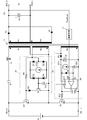
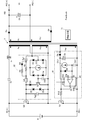
- FIG. 8 is a circuit diagram of the switching power supply device of the first embodiment.
- the voltage of the input power source Vi is input between the input terminals PI (+)-PI ( ⁇ ) of the switching power supply device 101.
- a predetermined DC voltage Vo is output to a load (not shown) connected between the output terminals PO (+) and PO ( ⁇ ) of the switching power supply device 101.
- a first series circuit in which a resonant capacitor Cr, a resonant inductor Lr, a primary winding np of a transformer T, and a low-side switching element Q1 are connected in series (the present invention).
- the resonant inductor Lr is a leakage inductance of the transformer T.
- the resonant inductor Lr may be an inductor connected to the primary winding np of the transformer T separately from the leakage inductance of the transformer T.
- the low-side switching element Q1 is composed of an n-type MOS-FET, and its drain terminal is connected to the primary winding np of the transformer T.
- a second series circuit in which a high-side switching element Q2, a resonance capacitor Cr, and a resonance inductor Lr are connected in series is configured at both ends of the primary winding np of the transformer T.
- the secondary winding ns of the transformer T has a center tap, and the secondary windings ns1 and ns2 are connected in series.
- the secondary windings ns1 and ns2 are bifilar wound to form the secondary winding ns shown in FIG.
- a rectifying and smoothing circuit including diodes Ds and Df and a capacitor Co is configured in the secondary windings ns1 and ns2. This rectifying / smoothing circuit performs full-wave rectification and smoothing of the AC voltage output from the secondary windings ns1, ns2, and outputs it to the output terminals PO (+)-PO (-).
- a low-side switching control unit (switching control circuit of the present invention) 81 is connected to the drive winding (hereinafter referred to as low-side drive winding) nb1 of the transformer T.
- the low-side switching control unit 81 includes a rectifying / smoothing circuit including a diode Db and a capacitor Cb.
- a DC voltage obtained by the rectifying / smoothing circuit is supplied as a power supply voltage to the VCC terminal of the switching control IC 84.
- the switching control IC 84 is a general-purpose switching control IC that operates in a current mode.
- a feedback circuit is provided between the output terminals PO (+) and PO ( ⁇ ) and the switching control IC 84.
- the return path is simply represented by a single line (Feedback).
- An insulating means 71 is provided in the return path, and for example, a photocoupler or a pulse transformer can be used.
- a feedback signal is generated by comparing the divided value of the DC voltage Vo between the output terminals PO (+) and PO ( ⁇ ) with a reference voltage, and the feedback voltage is supplied to the FB terminal of the switching control IC 84 in an insulated state. Enter.
- the feedback voltage input to the FB terminal increases as the DC voltage Vo decreases.
- the switching control IC 84 includes an OUT terminal and a ZT terminal.
- the OUT terminal of the switching control IC 84 is connected to the gate terminal of the low-side switching element Q1 via the resistor R12.
- the voltage generated from the low-side drive winding nb1 is input to the ZT terminal of the switching control IC 84.
- the switching control IC 84 includes a voltage polarity inversion detection circuit and a turn-off delay circuit that detect that the input voltage at the ZT terminal is inverted.
- the voltage polarity inversion detection circuit includes a comparator that compares an internally generated reference voltage with the voltage at the ZT terminal. When the output voltage of the comparator becomes low level, the OUT terminal is set to low level after the delay time td1 by the turn-off delay circuit.
- the low-side switching element Q1 is turned off. Further, when the output of the comparator becomes high level, the OUT terminal is inverted to high level after a delay time td0 described later has elapsed. As a result, the low-side switching element Q1 is turned on.
- the voltage waveform generated in the low-side drive winding nb1 is similar to the voltage waveform generated in the primary winding np.
- the voltage waveform generated in the low-side drive winding nb1 is similar to the waveform obtained by adding the voltage waveform generated in the excitation inductance of the primary winding np and the voltage waveform generated in the resonant inductor Lr.
- the switching control IC 84 detects the reversal of the voltage polarity generated in the low-side drive winding nb1, appropriately detects the resonance timing, and turns on the low-side switching element Q1 to turn on the low-side switching element Q1. ZVS operation can be performed reliably. Further, by appropriately detecting the resonance timing, the resonance state can be detected appropriately, and “resonance failure” can be prevented.
- a series circuit of a constant current circuit CC1 and a capacitor Cb1 is connected to the OUT terminal of the switching control IC 84 so that the charging voltage of the capacitor Cb1 is input to the IS terminal.
- the constant current circuit CC1 charges the capacitor Cb1 with a constant current by the voltage of the OUT terminal of the switching control IC 84.
- the comparator in the switching control IC 84 compares the voltage of the capacitor Cb1 with the voltage of the FB terminal, and when the voltage of the IS terminal exceeds the voltage of the FB terminal, the voltage of the OUT terminal is changed from the high level to the low level. Therefore, the lower the voltage at the FB terminal, the shorter the charging time of the capacitor Cb1. That is, the ON time of the low-side switching element Q1 is shortened, and the DC voltage Vo is made constant.
- the diode D9 constitutes a discharge path for the charge of the capacitor Cb1. That is, when the output voltage of the switching control IC 84 becomes low level (when Q1 is turned off), the charge in the capacitor Cb1 is discharged through the diode D9.
- the circuit including the switching control IC 84, the constant current circuit CC1, and the capacitor Cb1, which are ICs operating in the current mode functions as a voltage-time conversion circuit.
- the voltage of the feedback signal generated by detecting the DC voltage Vo and comparing it with the reference voltage is converted by the voltage-time conversion circuit, and the low-side switching element Q1 is turned on for that time.
- a high-side switching control unit (a switching control circuit of the present invention) 61 is provided between the drive winding (hereinafter referred to as a high-side drive winding) nb2 of the transformer T and the high-side switching element Q2. Specifically, the first end of the high-side drive winding nb2 of the transformer T is connected to the connection point (source terminal of the high-side switching element Q2) between the low-side switching element Q1 and the high-side switching element Q2, and the high-side drive A high-side switching control unit 61 is connected between the second end of the winding nb2 and the gate terminal of the high-side switching element Q2.
- the high-side switching control unit 61 includes a diode bridge rectifier circuit including four diodes D1, D2, D3, and D4, and a connection point between the diodes D1 and D3 and a connection point between the diodes D2 and D4.
- This is a bidirectional constant current circuit composed of a constant current circuit CC2 connected between the output terminals of the diode bridge rectifier circuit.
- the high-side switching control unit 61 is configured with a turn-on delay circuit that delays the turn-on by a delay time td2, which will be described later, by the input capacitance (gate-source capacitance) of the resistor R5 and the high-side switching element Q2.
- This turn-on delay circuit turns on the high-side switching element Q2 after a delay time td2 has elapsed since the polarity of the voltage generated in the high-side drive winding nb2 is reversed.
- the high side drive winding nb2 since the high side drive winding nb2 is wound close to the secondary winding ns, the coupling between the high side drive winding nb2 and the secondary winding ns is strong.
- the voltage waveform generated in the high-side drive winding nb2 is similar to the voltage waveform generated in the secondary winding ns, that is, the voltage waveform generated in the excitation inductance of the secondary winding ns.
- the high-side switching control unit 61 can perform the ZVS operation by turning on the high-side switching element Q2 at the timing when the voltage is generated in the secondary winding ns.
- the high side switching control unit 61 forcibly turns off the high side switching element Q2 when the same time as the on time of the low side switching element Q1 has elapsed after the high side switching element Q2 is turned on.
- the high side switching element Q2 is turned off at the timing determined by the time constant circuit regardless of the resonance condition.
- FIG. 9 is a waveform diagram showing changes in the voltage Vnb2 of the high-side drive winding nb2 and the base-emitter voltage Vbe of the transistor Q3 when there is a load change.
- TQ1ON (1) and TQ2ON (1) are equal by the above-described operation. Even when the on-time of the low-side switching element Q1 becomes long and becomes TQ1ON (2), TQ1ON (2) and TQ2ON (2) are equal by the above-described operation.
- FIG. 10 shows the gate-source voltage Vgs1 of the low-side switching element Q1, the gate-source voltage Vgs2 of the high-side switching element Q2, the drain-source voltage Vds1 of the low-side switching element Q1, the base-emitter voltage of the transistor Q3 ( It is a wave form diagram which shows the relationship between voltage Cbe of capacitor Cb2, Vbe, voltage of IS terminal of switching control IC84 (voltage of capacitor Cb1) Vis, and voltage Vzt of ZT terminal.
- the operation of the switching power supply device 101 will be described based on FIG. The operation of one cycle of the switching power supply device 101 is as follows.
- the switching control IC 84 detects that the polarity of the winding voltage generated in the low-side drive winding nb1 of the transformer T is inverted based on the input voltage of the ZT terminal, and the delay time td1 from the time when this polarity inversion is detected.
- the low side switching element Q1 is turned off with a delay.
- the capacitor Cb2 is discharged via the constant current circuit CC2.
- the low-side switching element Q1 is turned off at a time generated by a signal voltage based on a feedback signal (Feedback) for controlling the DC voltage Vo.
- Feeback feedback signal
- the high-side switching element Q2 When the low-side switching element Q1 is turned off, the high-side switching element Q2 is charged after the input capacitance (capacitance between the gate and the source) of the high-side switching element Q2 is charged by the winding voltage generated in the high-side driving winding nb2. Turn on. Therefore, the high side switching element Q2 is turned on with a delay of the delay time td2 due to the charging.
- the capacitor Cb2 is charged via the constant current circuit CC2.
- the transistor Q3 When the charging voltage Vbe of the capacitor Cb2 reaches the threshold voltage of the transistor Q3, the transistor Q3 is turned on, the input capacitance of the high side switching element Q2 is rapidly discharged, and the high side switching element Q2 is turned off.
- the switching control IC 84 detects this based on the input voltage at the ZT terminal.
- the low-side switching element Q1 is turned on after the elapse of the delay time td0 from the reversal of the voltage polarity.
- FIG. 11A is a waveform diagram of the voltage of the primary winding np of the transformer T and the drain current of the low-side switching element Q1 in a normal state without “loss of resonance”.
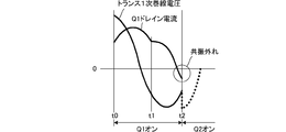
- FIG. 11B is a waveform diagram of the voltage of the primary winding np of the transformer T and the drain current of the low-side switching element Q1 in a state where “loss of resonance” occurs.
- the section from t0 to t1 of the waveform of the drain current is a current waveform based on the series resonance of the resonant inductor (including the leakage inductance of the primary winding np) Lr and the resonant capacitor Cr having a relatively small inductance value.
- the section from t1 to t2 is a current waveform based on the series resonance of the resonant inductor Lr, the exciting inductance of the transformer T, and the resonant capacitor Cr.
- the switching frequency is represented by fs and the resonance frequency of the first series circuit is represented by fm
- the relationship of fm ⁇ fs is maintained in normal operation.
- the switching frequency fs increases and the output power decreases.
- the switching frequency fs decreases and the output power increases.
- the current flowing through the primary winding np of the transformer T operates in a “current delay phase” in which the phase is delayed from the voltage applied to the primary winding np.
- the switching frequency fs decreases, and when fs ⁇ fm, the resonance condition is removed (“out of resonance”). That is, the relationship in which the switching frequency fs is lower than the resonance frequency fm is a state where the transformer T appears as a capacitive impedance from the primary side of the transformer T, and the current is larger than the phase of the voltage waveform applied to the primary winding np of the transformer T. The phase of the waveform will advance. In this case, a period in which the low-side switching element Q1 and the high-side switching element Q2 are simultaneously turned on (so-called arm short-circuit state) occurs, and an excessive current flows through the two switching elements Q1 and Q2, resulting in a large loss. To do.
- the high-side switching element Q2 when the phase of the current waveform is advanced from the phase of the voltage waveform, the high-side switching element Q2 is turned on with a dead time after the low-side switching element Q1 is turned off, but flows to the low-side switching element Q1.
- the high-side switching element Q2 is turned on in the state where the current direction is already reversed (flowing through the body diode of the low-side switching element Q1), the low-side switching element Q1 is delayed due to the delay of the cutoff due to the reverse recovery characteristic of the body diode.
- the high-side switching element Q2 becomes conductive while the body diode is conductive, and the arm short circuit occurs. Further, in a state where the phase of the current waveform is ahead of the phase of the voltage waveform, the ZVS operation cannot be performed and the switching loss increases.
- the switching control IC 84 when the OUT terminal voltage of the switching control IC 84 is high and the voltage at the ZT terminal decreases to near 0 V, the switching control IC 84 is low side.
- the switching element Q1 is forcibly turned off. This forced turn-off operation is performed earlier than the high-side switching element Q2 is turned on. That is, the delay time td1 from the timing when the polarity of the winding voltage generated in the low-side drive winding nb1 is detected as a starting point until the low-side switching element Q1 is turned off is the input capacitance of the high-side switching element Q2.
- Td1 and td2 are determined so as to satisfy the condition (td1 ⁇ td2) that is shorter than the delay time td2 until the high-side switching element Q2 is turned on.
- the switching frequency fs does not fall below the resonance frequency fm and the resonance condition is not removed, and the low-side switching element Q1 is turned on even in a transient operation state such as starting, stopping, or output short-circuiting. Even if the winding voltage of the primary winding np is inverted later, the high-side switching element Q2 is not turned on before Q1 is turned off based on the feedback signal. In other words, the destruction of the switching power supply device 101 can prevent an increase in loss without causing an arm short circuit.
- the switching control IC 84 shown in FIG. 8 includes a circuit for setting a blanking time. Specifically, the signal input to the ZT terminal is not detected for a predetermined period (set blanking time) after generating a pulse for driving the low-side switching element Q1. That is, the input of the ZT terminal is masked. Thus, by setting the blanking time during which the polarity of the winding voltage is not detected for a predetermined period, switching noise that becomes a signal that turns on the low-side switching element Q1 is generated at the ZT terminal during the blanking time. Even if it is input, it is possible to prevent a malfunction that causes the low-side switching element Q1 to be turned on by a noise signal.
- a delay circuit that generates the delay time td2 includes a resistor R5 (impedance circuit) connected in series to the control terminal of the high-side switching element Q2 and an input capacitance (gate-source) existing at the gate terminal of the high-side switching element Q2. The number of parts is reduced, and the switching power supply device can be downsized.
- FIG. 12 is a circuit diagram of the switching power supply device according to the second embodiment. Except for the high-side switching control unit 62 of the switching power supply device 102, the circuit is the same as the circuit shown in FIG. 8 in the first embodiment.
- An impedance circuit composed of a capacitor Cg1, a diode D6, resistors R5, R6, and an inductor Lg is connected to the high side switching control unit 62 between the output of the high side driving winding nb2 and the high side switching element Q2. ing.
- the inductor Lg is a chip inductor or a bead inductor.
- a series circuit of Zener diodes ZD1 and ZD2 and a capacitor Cg2 are connected between the gate and source of the high-side switching element Q2.
- Other configurations in the high-side switching control unit 62 are the same as those of the high-side switching control unit 61 shown in FIG.
- the turn-on delay circuit of the high side switching element Q2 is constituted by the impedance circuit and the capacitor Cg2 connected between the output of the high side driving winding nb2 and the control terminal of the high side switching element Q2.
- the capacitor Cg2 is charged by the winding voltage generated in the high side drive winding nb2, and when the gate-source voltage of the high side switching element Q2 exceeds the threshold value, Q2 is turned on.
- the capacitor Cg1 controls the voltage value between the gate and the source of the high-side switching element Q2 by the capacitance division with the capacitor Cg2.
- Zener diodes ZD1 and ZD2 limit the maximum change width of the voltage value between the gate and source of high-side switching element Q2.
- the impedance circuit which is a part of the turn-on delay circuit of Q2 changes its impedance according to the direction of current, the turn-on speed and the turn-off speed of the switching element Q2 are individually set. Can be adjusted.
- the impedance circuit is composed of a series circuit of the capacitor Cg1 and the resistors R5 and R6, by adjusting the capacitance value of the capacitor Cg1, it is possible to obtain the input capacitance existing at the gate terminal of the high-side switching element Q2.
- An appropriate gate voltage can be applied to adjust the voltage division ratio and turn the high-side switching element Q2 on and off.
- the inductor Lg is provided in the impedance circuit, it is possible to suppress high-frequency surge current and prevent an excessive voltage from being applied to the gate terminal of the high-side switching element Q2.
- Zener diode is connected bidirectionally in parallel between the gate and source of the high side switching element Q2, it is possible to prevent an excessive voltage from being applied to the gate terminal of the high side switching element Q2.
- the Zener diode connected in parallel between the gate and source of the high-side switching element Q2 may be connected only in any one direction.
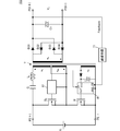
- FIG. 13 is a circuit diagram of the switching power supply device according to the third embodiment.
- the difference from the switching power supply device shown in FIG. 8 in the first embodiment is the configuration on the secondary side of the transformer T.
- the diode bridge circuit and the capacitor Co by the diodes D21, D22, D23, and D24 are connected to the secondary winding ns of the transformer T.
- full-wave rectification may be performed by the diode bridge circuit.
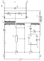
- FIG. 14 is a circuit diagram of a switching power supply device according to the fourth embodiment.
- the switching power supply 104 according to the fourth embodiment differs from the switching power supply shown in FIG. 8 in the first embodiment in the configuration on the secondary side of the transformer T.
- a rectifying and smoothing circuit including a diode Ds and a capacitor Co1 is configured at both ends of the secondary winding ns1 of the transformer T, and the capacitor Co3 is connected between the output terminals PO (+) and PO ( ⁇ ). .
- the midpoint of the series circuit of the diode Df and the capacitor Co2 is connected to the output terminal PO ( ⁇ ), and both ends are connected to both ends of the secondary winding ns1 of the transformer T.
- a voltage doubler rectifier circuit may be used.
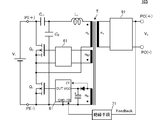
- FIG. 15 is a circuit diagram of a switching power supply device according to the fifth embodiment.
- the switching power supply device 105 according to the fifth embodiment is different from the above-described embodiments in that the resonant capacitor Cr1 and the resonant inductor are provided between the drain of the high-side switching element Q2 and one end of the primary winding np of the transformer T.
- a resonance capacitor Cr2 is provided between the connection point of the resonance capacitor Cr1 and the resonance inductor Lr and the ground line.
- the resonant capacitor Cr1 is provided so that the resonant inductor Lr, the primary winding np, the high-side switching element Q2, and the resonant capacitor Cr1 form a closed loop.
- the resonance capacitor Cr2 is provided so that the resonance inductor Lr, the primary winding np, the low-side switching element Q1, and the resonance capacitor Cr2 form a closed loop.
- the current supplied from the input power source Vi is such that the resonance capacitor Cr1, during both the on-time of the low-side switching element Q1 and the on-time of the high-side switching element Q2, It flows into Cr2.
- the effective current of the current supplied from the input power source Vi is reduced. Thereby, the conduction loss due to the current supplied from the input power source Vi can be reduced.
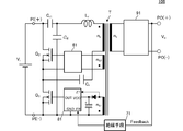
- FIG. 16 is a circuit diagram of a switching power supply device according to the sixth embodiment.
- the switching power supply device 106 according to the sixth embodiment is different from the switching power supply device shown in FIG. 8 in the first embodiment in that resonance capacitors Cr1 and Cr2 are provided in addition to the resonance capacitor Cr.
- the resonance inductor Lr, the primary winding np, the resonance capacitor Cr, and the high side switching element Q1 so that the resonance inductor Lr, the primary winding np, the resonance capacitor Cr, the high side switching element Q2, and the resonance capacitor Cr1 constitute a closed loop.
- the resonance capacitors Cr1 and Cr2 are provided so that the resonance capacitor Cr2 forms a closed loop.
- the resonance capacitors Cr1 and Cr2 are connected so as to divide the voltage of the input power source Vi.
- a plurality of resonant capacitors (Cr, Cr1, Cr2) through which a resonant current flows may be provided.
- a rectifying and smoothing circuit 91 is connected to the secondary winding ns of the transformer T.
- the rectifying / smoothing circuit 91 is a rectifying / smoothing circuit including the diodes Ds and Df and the capacitor Co shown in FIG.
- a rectifier circuit using a diode is configured in the circuit on the secondary side of the transformer T.
- a rectifying FET may be provided for synchronous rectification. This can reduce the loss of the secondary side circuit.
- the present invention can be applied not only to a half-bridge converter but also to a switching power supply device that alternately turns on / off two switching elements in a multi-stone converter such as a full-bridge converter, a voltage clamp converter, and the like. .
- the transformer according to the present invention can secure a distance on the safety standard without weakening the magnetic field coupling between the primary winding np and the secondary winding ns. This effect does not change even when the transformer does not include the drive windings nb1 and nb2.
- the height of the primary winding np and the secondary winding ns may be substantially the same.
Landscapes
- Engineering & Computer Science (AREA)
- Power Engineering (AREA)
- Physics & Mathematics (AREA)
- Nonlinear Science (AREA)
- Dc-Dc Converters (AREA)
- Coils Of Transformers For General Uses (AREA)
- Medicines That Contain Protein Lipid Enzymes And Other Medicines (AREA)
- Ignition Installations For Internal Combustion Engines (AREA)
Description
図1は実施形態1に係るトランスのボビンの断面図である。図2は実施形態1に係るトランスの三面図である。図3は図2のIII-III線の断面図である。図4はトランスのカバーの三面図である。図5は図4のV-V線の断面図である。図6はトランスの磁性体コアの上面図及び右側面図である。
図12は実施形態2に係るスイッチング電源装置の回路図である。このスイッチング電源装置102のハイサイドスイッチング制御部62以外は、第1の実施形態で図8に示した回路と同じである。
図13は実施形態3に係るスイッチング電源装置の回路図である。実施形態1で図8に示したスイッチング電源装置と異なるのは、トランスTの二次側の構成である。
図14は実施形態4に係るスイッチング電源装置の回路図である。実施形態4に係るスイッチング電源装置104が実施形態1で図8に示したスイッチング電源装置と異なるのは、トランスTの二次側の構成である。
図15は実施形態5に係るスイッチング電源装置の回路図である。実施形態5に係るスイッチング電源装置105が以上に示した各実施形態と異なるのは、ハイサイドスイッチング素子Q2のドレインとトランスTの1次巻線npの一端との間に共振キャパシタCr1と共振インダクタLrの直列回路を設けるだけでなく、共振キャパシタCr1と共振インダクタLrとの接続点とグランドラインとの間に共振キャパシタCr2を設けた点である。
図16は実施形態6に係るスイッチング電源装置の回路図である。実施形態6に係るスイッチング電源装置106が実施形態1で図8に示したスイッチング電源装置と異なるのは、共振キャパシタCr以外に共振キャパシタCr1,Cr2を設けた点である。
11-筒形状部(巻回部)
13,14-仕切板(仕切部)
15-スリット
20-カバー
24-凸部
30,31-磁性体コア
61,62-ハイサイドスイッチング制御部(スイッチング制御回路)
81-ローサイドスイッチング制御部(スイッチング制御回路)
84-スイッチング制御IC
101~106-スイッチング電源装置
Cr-共振キャパシタ
Lr-共振インダクタ
nb1-ローサイド駆動巻線
nb2-ハイサイド駆動巻線
np-1次巻線
ns1,ns2-2次巻線
PI-入力端子
PO-出力端子
Q1-ローサイドスイッチング素子
Q2-ハイサイドスイッチング素子
T-トランス
Vi-入力電源
Vo-出力電圧
Claims (7)
- 入力電源電圧が入力される電源電圧入力部と、
直流電圧が出力される直流電圧出力部と、
ボビンの巻回部に巻回された1次巻線及び2次巻線、ローサイド駆動巻線及びハイサイド駆動巻線、並びに、閉磁路を形成するコアを有するトランスと、
前記1次巻線を含んでLC共振回路を形成するキャパシタと、
前記電源電圧入力部に接続される、ローサイドスイッチング素子とハイサイドスイッチング素子との直列回路と、
前記ローサイドスイッチング素子を制御するローサイドスイッチング制御部と、前記ハイサイドスイッチング素子を制御するハイサイドスイッチング制御部とを有するスイッチング制御回路と、
を備え、
前記LC共振回路は、前記トランスの前記1次巻線又は前記2次巻線の漏れインダクタンスを含み、
前記ローサイドスイッチング素子は、前記1次巻線に直列接続されて、オンにより前記電源電圧入力部の電圧を前記1次巻線に印加し、
前記ローサイドスイッチング制御部は、前記ローサイド駆動巻線に発生する巻線電圧の極性反転を検出して前記ローサイドスイッチング素子をターンオンし、出力電圧を検出する回路の帰還信号に基づく時間で前記ローサイドスイッチング素子をターンオフし、
前記ハイサイドスイッチング制御部は、前記ハイサイド駆動巻線に発生する巻線電圧の極性反転を検出して前記ハイサイドスイッチング素子をターンオンし、前記ローサイドスイッチング素子のオン時間に応じて前記ハイサイドスイッチング素子をターンオフし、
前記ボビンはスリットを有する仕切り部を備え、
前記仕切り部は、前記巻回部の外周に沿って設けられ、前記巻回部を前記1次巻線が巻回される第1巻回領域と前記2次巻線が巻回される第2巻回領域とに分割し、
前記1次巻線は、前記巻回部の外周面から第1の高さh1まで巻回され、
前記2次巻線は、前記巻回部の外周面から第2の高さh2まで巻回され、
前記ローサイド駆動巻線及び前記ハイサイド駆動巻線は、前記ハイサイド駆動巻線を前記2次巻線側にして巻回軸方向に沿って併設されて、前記1次巻線に巻回されている、
スイッチング電源装置。 - 前記スリットと嵌合する凸部を有し、前記1次巻線、前記2次巻線、前記ローサイド駆動巻線及び前記ハイサイド駆動巻線を覆うカバーを備えている、
請求項1に記載のスイッチング電源装置。 - 前記トランスが実装される基板に対向する側の前記仕切部の高さは、前記第2の高さh2より高い、請求項1又は2に記載のスイッチング電源装置。
- 前記仕切部は、前記巻回軸に沿った前記巻回部の長さの中央から外れた位置に設けられている、請求項1から3の何れかに記載のスイッチング電源装置。
- 前記2次巻線は、センタータップが取り出され、バイファイラ巻きされた第1の巻線と第2の巻線とを有している、請求項1から4の何れかに記載のスイッチング電源装置。
- 巻回軸の直交方向における前記コアの断面は、前記トランスの実装高さ寸法方向が最短長となる扁平形状である、請求項1から5の何れかに記載のスイッチング電源装置。
- 前記キャパシタは、前記ハイサイドスイッチング素子と前記ローサイドスイッチング素子との間に接続されている、請求項1から6の何れかに記載のスイッチング電源装置。
Priority Applications (4)
| Application Number | Priority Date | Filing Date | Title |
|---|---|---|---|
| JP2014507686A JP5776841B2 (ja) | 2012-03-30 | 2013-03-15 | スイッチング電源装置 |
| CN201380017140.3A CN104221266B (zh) | 2012-03-30 | 2013-03-15 | 开关电源装置 |
| GB1414559.3A GB2517312B (en) | 2012-03-30 | 2013-03-15 | Switching Power Supply Device |
| US14/481,031 US9257912B2 (en) | 2012-03-30 | 2014-09-09 | Switching power supply device |
Applications Claiming Priority (2)
| Application Number | Priority Date | Filing Date | Title |
|---|---|---|---|
| JP2012-080053 | 2012-03-30 | ||
| JP2012080053 | 2012-03-30 |
Related Child Applications (1)
| Application Number | Title | Priority Date | Filing Date |
|---|---|---|---|
| US14/481,031 Continuation US9257912B2 (en) | 2012-03-30 | 2014-09-09 | Switching power supply device |
Publications (1)
| Publication Number | Publication Date |
|---|---|
| WO2013146338A1 true WO2013146338A1 (ja) | 2013-10-03 |
Family
ID=49259599
Family Applications (1)
| Application Number | Title | Priority Date | Filing Date |
|---|---|---|---|
| PCT/JP2013/057371 Ceased WO2013146338A1 (ja) | 2012-03-30 | 2013-03-15 | スイッチング電源装置 |
Country Status (5)
| Country | Link |
|---|---|
| US (1) | US9257912B2 (ja) |
| JP (1) | JP5776841B2 (ja) |
| CN (1) | CN104221266B (ja) |
| GB (1) | GB2517312B (ja) |
| WO (1) | WO2013146338A1 (ja) |
Cited By (1)
| Publication number | Priority date | Publication date | Assignee | Title |
|---|---|---|---|---|
| JP2023058185A (ja) * | 2021-10-13 | 2023-04-25 | 株式会社マキタ | 電動作業機 |
Families Citing this family (4)
| Publication number | Priority date | Publication date | Assignee | Title |
|---|---|---|---|---|
| US11246905B2 (en) | 2016-08-15 | 2022-02-15 | President And Fellows Of Harvard College | Treating infections using IdsD from Proteus mirabilis |
| CN108843585B (zh) * | 2018-08-13 | 2024-05-28 | 北京芯金源测控技术有限公司 | 一种集成液位识别功能的自动化电排水泵 |
| JP7157640B2 (ja) * | 2018-11-28 | 2022-10-20 | 株式会社Soken | 電力変換装置の制御装置 |
| JP7577980B2 (ja) * | 2020-11-27 | 2024-11-06 | 富士電機株式会社 | 電流検出回路、電源回路 |
Citations (2)
| Publication number | Priority date | Publication date | Assignee | Title |
|---|---|---|---|---|
| JP2008228382A (ja) * | 2007-03-09 | 2008-09-25 | Fuji Electric Device Technology Co Ltd | スイッチング電源装置 |
| JP2009142088A (ja) * | 2007-12-07 | 2009-06-25 | Hitachi Ltd | 表示装置用dc−dcコンバータ |
Family Cites Families (8)
| Publication number | Priority date | Publication date | Assignee | Title |
|---|---|---|---|---|
| JP3041842B2 (ja) | 1994-03-31 | 2000-05-15 | サンケン電気株式会社 | 共振型スイッチング電源 |
| JP3201383B2 (ja) | 1999-04-13 | 2001-08-20 | サンケン電気株式会社 | 共振型電源用トランス |
| JP3591635B2 (ja) * | 1999-12-08 | 2004-11-24 | 富士電機機器制御株式会社 | 直流−直流変換装置 |
| JP4423458B2 (ja) | 2000-11-10 | 2010-03-03 | 富士電機システムズ株式会社 | Dc/dcコンバータの制御方法 |
| US7768801B2 (en) * | 2004-12-08 | 2010-08-03 | Sanken Electric Co., Ltd. | Current resonant DC-DC converter of multi-output type |
| CN100590954C (zh) * | 2004-12-08 | 2010-02-17 | 三垦电气株式会社 | 多输出电流谐振型dc-dc变换器 |
| JP4525817B2 (ja) * | 2008-10-30 | 2010-08-18 | サンケン電気株式会社 | スイッチング電源装置 |
| JP5589701B2 (ja) * | 2010-09-15 | 2014-09-17 | 富士電機株式会社 | 力率改善電流共振コンバータ |
-
2013
- 2013-03-15 WO PCT/JP2013/057371 patent/WO2013146338A1/ja not_active Ceased
- 2013-03-15 CN CN201380017140.3A patent/CN104221266B/zh active Active
- 2013-03-15 JP JP2014507686A patent/JP5776841B2/ja active Active
- 2013-03-15 GB GB1414559.3A patent/GB2517312B/en active Active
-
2014
- 2014-09-09 US US14/481,031 patent/US9257912B2/en active Active
Patent Citations (2)
| Publication number | Priority date | Publication date | Assignee | Title |
|---|---|---|---|---|
| JP2008228382A (ja) * | 2007-03-09 | 2008-09-25 | Fuji Electric Device Technology Co Ltd | スイッチング電源装置 |
| JP2009142088A (ja) * | 2007-12-07 | 2009-06-25 | Hitachi Ltd | 表示装置用dc−dcコンバータ |
Cited By (3)
| Publication number | Priority date | Publication date | Assignee | Title |
|---|---|---|---|---|
| JP2023058185A (ja) * | 2021-10-13 | 2023-04-25 | 株式会社マキタ | 電動作業機 |
| US12408586B2 (en) | 2021-10-13 | 2025-09-09 | Makita Corporation | Electric work machine |
| JP7761445B2 (ja) | 2021-10-13 | 2025-10-28 | 株式会社マキタ | 電動作業機 |
Also Published As
| Publication number | Publication date |
|---|---|
| GB2517312A (en) | 2015-02-18 |
| GB2517312B (en) | 2019-03-06 |
| JP5776841B2 (ja) | 2015-09-09 |
| CN104221266A (zh) | 2014-12-17 |
| CN104221266B (zh) | 2016-11-02 |
| US9257912B2 (en) | 2016-02-09 |
| US20140376274A1 (en) | 2014-12-25 |
| GB201414559D0 (en) | 2014-10-01 |
| JPWO2013146338A1 (ja) | 2015-12-10 |
Similar Documents
| Publication | Publication Date | Title |
|---|---|---|
| JP5549659B2 (ja) | スイッチング電源装置 | |
| US7778048B2 (en) | Switching power supply apparatus | |
| JP4671019B2 (ja) | 多出力型dc−dcコンバータ | |
| US9385617B2 (en) | Overcurrent protection circuit for a switching power supply apparatus | |
| US6366476B1 (en) | Switching power supply apparatus with active clamp circuit | |
| JP4099593B2 (ja) | スイッチング電源回路 | |
| US8749996B2 (en) | Switching power supply apparatus | |
| KR100632688B1 (ko) | 스위칭 전원장치 | |
| JP2000152617A (ja) | スイッチング電源回路 | |
| JP5776841B2 (ja) | スイッチング電源装置 | |
| TW202201891A (zh) | 諧振半橋返馳電源供應器及其一次側控制電路與控制方法 | |
| JP2010178411A (ja) | 絶縁型スイッチング電源装置 | |
| TWI732581B (zh) | 具減震控制之轉換裝置及其減震控制的操作方法 | |
| JP5117980B2 (ja) | エネルギー伝達装置およびエネルギー伝達制御用半導体装置 | |
| KR20050045890A (ko) | 스위칭 전원회로 | |
| JP2001095247A (ja) | スイッチング電源回路 | |
| JP2005137040A (ja) | 非接触給電装置 | |
| WO2023065230A1 (en) | Hold-up time circuit for llc converter | |
| JP2005073335A (ja) | スイッチング電源回路 | |
| JP4367611B2 (ja) | スイッチング電源回路 | |
| JP4218092B2 (ja) | スイッチング電源回路 | |
| Chen et al. | 2nd Generation LLC Current Resonant Control IC,“FA6A00N Series” | |
| Karlsson et al. | Design and Analysis of a Phase Shifted Full Bridge Converter for High Efficiency Operation | |
| KR20160144858A (ko) | Llc 공진형 컨버터의 제어 회로 및 제어 방법 | |
| JP2005094981A (ja) | スイッチング電源回路 |
Legal Events
| Date | Code | Title | Description |
|---|---|---|---|
| 121 | Ep: the epo has been informed by wipo that ep was designated in this application |
Ref document number: 13770195 Country of ref document: EP Kind code of ref document: A1 |
|
| ENP | Entry into the national phase |
Ref document number: 1414559 Country of ref document: GB Kind code of ref document: A Free format text: PCT FILING DATE = 20130315 |
|
| WWE | Wipo information: entry into national phase |
Ref document number: 1414559.3 Country of ref document: GB |
|
| ENP | Entry into the national phase |
Ref document number: 2014507686 Country of ref document: JP Kind code of ref document: A |
|
| NENP | Non-entry into the national phase |
Ref country code: DE |
|
| 122 | Ep: pct application non-entry in european phase |
Ref document number: 13770195 Country of ref document: EP Kind code of ref document: A1 |