WO2013190850A1 - Appareil d'informations - Google Patents
Appareil d'informations Download PDFInfo
- Publication number
- WO2013190850A1 WO2013190850A1 PCT/JP2013/003886 JP2013003886W WO2013190850A1 WO 2013190850 A1 WO2013190850 A1 WO 2013190850A1 JP 2013003886 W JP2013003886 W JP 2013003886W WO 2013190850 A1 WO2013190850 A1 WO 2013190850A1
- Authority
- WO
- WIPO (PCT)
- Prior art keywords
- strain
- strain detection
- stress concentration
- substrate
- information device
- Prior art date
- Legal status (The legal status is an assumption and is not a legal conclusion. Google has not performed a legal analysis and makes no representation as to the accuracy of the status listed.)
- Ceased
Links
Images










Classifications
-
- G—PHYSICS
- G06—COMPUTING OR CALCULATING; COUNTING
- G06F—ELECTRIC DIGITAL DATA PROCESSING
- G06F3/00—Input arrangements for transferring data to be processed into a form capable of being handled by the computer; Output arrangements for transferring data from processing unit to output unit, e.g. interface arrangements
- G06F3/01—Input arrangements or combined input and output arrangements for interaction between user and computer
- G06F3/03—Arrangements for converting the position or the displacement of a member into a coded form
- G06F3/041—Digitisers, e.g. for touch screens or touch pads, characterised by the transducing means
- G06F3/0414—Digitisers, e.g. for touch screens or touch pads, characterised by the transducing means using force sensing means to determine a position
-
- G—PHYSICS
- G06—COMPUTING OR CALCULATING; COUNTING
- G06F—ELECTRIC DIGITAL DATA PROCESSING
- G06F3/00—Input arrangements for transferring data to be processed into a form capable of being handled by the computer; Output arrangements for transferring data from processing unit to output unit, e.g. interface arrangements
- G06F3/01—Input arrangements or combined input and output arrangements for interaction between user and computer
- G06F3/048—Interaction techniques based on graphical user interfaces [GUI]
- G06F3/0484—Interaction techniques based on graphical user interfaces [GUI] for the control of specific functions or operations, e.g. selecting or manipulating an object, an image or a displayed text element, setting a parameter value or selecting a range
- G06F3/04847—Interaction techniques to control parameter settings, e.g. interaction with sliders or dials
-
- G—PHYSICS
- G06—COMPUTING OR CALCULATING; COUNTING
- G06F—ELECTRIC DIGITAL DATA PROCESSING
- G06F3/00—Input arrangements for transferring data to be processed into a form capable of being handled by the computer; Output arrangements for transferring data from processing unit to output unit, e.g. interface arrangements
- G06F3/01—Input arrangements or combined input and output arrangements for interaction between user and computer
- G06F3/048—Interaction techniques based on graphical user interfaces [GUI]
- G06F3/0484—Interaction techniques based on graphical user interfaces [GUI] for the control of specific functions or operations, e.g. selecting or manipulating an object, an image or a displayed text element, setting a parameter value or selecting a range
- G06F3/0485—Scrolling or panning
-
- H—ELECTRICITY
- H04—ELECTRIC COMMUNICATION TECHNIQUE
- H04M—TELEPHONIC COMMUNICATION
- H04M1/00—Substation equipment, e.g. for use by subscribers
- H04M1/02—Constructional features of telephone sets
- H04M1/23—Construction or mounting of dials or of equivalent devices; Means for facilitating the use thereof
Definitions
- the present invention relates to an information device capable of performing various controls such as scrolling, enlarging, reducing, and adjusting a volume of a display screen with a simple operation based on a compressive load applied to a casing.
- Information devices such as digital cameras, notebook PCs, portable game machines, mobile phones, and personal digital assistants (PDAs) that can be carried and used by users are known.
- PDAs personal digital assistants
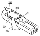
- FIG. 19 is a perspective view of a mobile phone 201 which is a conventional information device described in Patent Document 1.
- a display unit 202 such as a liquid crystal display on which characters, numbers, symbols, and the like are displayed is provided on the front surface of the mobile phone 201.
- a scroll operation unit 203 including a touch pad for performing a horizontal scrolling operation of the display screen with the user's finger 205 is provided.
- a scroll operation unit 204 including a touch pad for performing a vertical scrolling operation of the display screen with the user's finger 205 is provided near the left side of the display unit 202.
- the user can operate the display screen in two-dimensional directions such as up and down and left and right using the scroll operation units 203 and 205.
- FIG. 20 is a plan view of a mobile phone 206, which is another conventional information device described in Patent Document 2.
- the cellular phone 206 includes a rectangular thin casing, a display screen 211 provided on the front surface of the casing, and touch pads 207 to 210 provided on four side surfaces of the casing, respectively.
- the touch pads 207 to 210 have an elongated shape arranged so that the longitudinal direction thereof is parallel to the display screen 211. By performing a slide operation on the touch pads 207 to 210 in a direction parallel to the display screen 211, the display screen 211 can be scrolled, the display image can be rotated, and the display magnification can be changed.
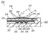
- FIG. 21 is an enlarged view of the input device 212 which is still another information device described in Patent Document 3.
- the input device 212 detects a user's sliding operation by a sensor provided in the housing 213 instead of the touch pad, and operates the screen.
- the input device 212 includes a flexible electrostatic sensor sheet mounting substrate 214 (hereinafter simply referred to as an FPC substrate 214) provided in the housing 213.
- an FPC substrate 2114 On the surface of the sheet-like FPC board 214, a sensor sheet 215 for tracing is arranged.
- the sensor sheet 215 constitutes an electrostatic sensor sheet.
- the sensor sheet 215 provided on the surface of the FPC board 214 is pressed by the key part 219 provided on the key part 218 by the sliding operation of the operator's finger 217 or the like on the key top 216, and the contact electrode 220 is moved to the dome switch. It operates so as to contact the projection 222 via the 221 to detect the sliding position and to output a position detection signal.
- the information equipment includes a housing, first and second strain detection elements that detect strain applied to the side surface of the housing, and first and second strain detection elements that detect strain applied to the side surface of the housing. Are provided with first and second stress concentrating portions, respectively. For the same amount of strain applied to the side surface of the housing, the output value output from the first strain detection element to the processing circuit is the same as the output value output from the second strain detection element to the processing circuit. Different.
- This information device can be miniaturized and can be controlled with high accuracy.
- FIG. 1A is a plan view of an information device according to Embodiment 1 of the present invention.
- 1B is a cross-sectional view of the information device shown in FIG. 1A taken along line 1B-1B.
- FIG. 2A is a plan view of a strain detection element of the information device according to Embodiment 1.
- 2B is a cross-sectional view of the strain sensing element shown in FIG. 2A along line 2B-2B.
- FIG. 3 is an enlarged view of the information device in the first embodiment.
- FIG. 4A is a diagram showing output characteristics of the strain detection element of the information device in the first exemplary embodiment.
- FIG. 4B is a diagram showing output characteristics of the strain detection element of the information device according to Embodiment 1.
- FIG. 4A is a diagram showing output characteristics of the strain detection element of the information device in the first exemplary embodiment.
- FIG. 4B is a diagram showing output characteristics of the strain detection element of the information device according to Embodiment 1.
- FIG. 5 is an enlarged view of an information device according to Embodiment 2 of the present invention.
- FIG. 6 is an enlarged view of an information device according to Embodiment 3 of the present invention.
- FIG. 7 is a diagram showing the sensitivity characteristics of the strain detection element of the information equipment in the third embodiment.
- FIG. 8 is an enlarged view of an information device according to Embodiment 4 of the present invention.
- FIG. 9 is an enlarged view of an information device according to Embodiment 5 of the present invention.
- FIG. 10 is a diagram showing the output characteristics of the strain detection element of the information equipment in the fifth embodiment.
- FIG. 11 is an enlarged view of an information device according to Embodiment 6 of the present invention.
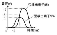
- FIG. 12A is a diagram showing the output of the strain detection element of the information equipment in Embodiment 6.
- FIG. 12B is a diagram showing the output of the strain detection element of the information equipment in Embodiment 6.
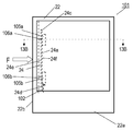
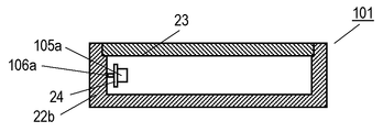
- FIG. 13A is a plan view of an information device according to Embodiment 7 of the present invention. 13B is a cross-sectional view taken along line 13B-13B of the information device shown in FIG. 13A.
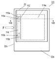
- FIG. 14A is a plan view of an information device according to Embodiment 8 of the present invention. 14B is a cross-sectional view of the information device shown in FIG. 14A taken along line 14B-14B.
- FIG. 15 is a plan view of an information device according to Embodiment 9 of the present invention.
- FIG. 16A is an enlarged view of an information device according to Embodiment 9.
- FIG. 16B is a plan view of another information device according to Embodiment 9.
- FIG. 17 is an enlarged view of the information device according to the tenth embodiment of the present invention.
- FIG. 18 is an enlarged view of the substrate of the information device according to the tenth embodiment.
- FIG. 19 is a plan view of a conventional information device.
- FIG. 20 is an external perspective view of another conventional information device.
- FIG. 21 is an enlarged view of still another conventional information device.
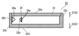
- FIG. 1A is a plan view of information device 21 according to Embodiment 1 of the present invention.
- 1B is a cross-sectional view taken along line 1B-1B of information device 21 shown in FIG. 1A.
- the housing 22 has a front surface 22a, a back surface 22d located on the opposite side of the front surface 22a, and side surfaces 22b and 22c connected to the front surface 22a and the back surface 22d.
- the side surfaces 22b and 22c are located on opposite sides of the front surface 22a.
- a display screen 23 such as a liquid crystal screen and operation keys are provided on the front surface 22a.
- the information device 21 includes a housing 22, a substrate 24 connected to the housing 22 by an internal chassis, strain detection elements 25 a and 25 b provided on the substrate 24, and stress provided on the side surface 22 b of the housing 22.
- the strain detection elements 25a and 25b face the side surface 22b.
- the stress concentration portions 26a and 26b face the strain detection elements 25a and 25b, respectively. As shown in FIG.
- the stress concentration portion 26a is longer in the thickness direction than the stress concentration portion 26b, and the distance L1 from the strain detection element 25a to the stress concentration portion 26a and from the strain detection element 25b to the stress concentration portion 26b.
- the distance L2 is different, and the distance L1 is smaller than the distance L2.
- An electronic component such as a CPU is mounted on the substrate 24 and is electrically connected to the strain detection element 25b. When distortion occurs on the back surface 22d, it is transmitted to the strain detection elements 25a and 25b by the stress concentration portions 26a and 26b, and electrical signals generated from the strain detection elements 25a and 25b due to the distortion are transmitted by the processing circuit 24a on the substrate 24. It is processed.
- the processing circuit 24a outputs an audio signal to the audio output unit 24b, and the audio output unit 24b outputs audio by the audio signal.
- the stress concentration portions 26a and 26b may be formed integrally with the side surface 22b, or may be attached to the side surface 22b with an adhesive or the like.
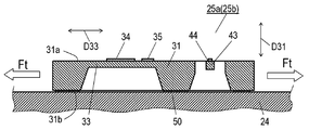
- FIG. 2A is a plan view of the strain detection element 25a (25b) of the information device 21 according to the first embodiment.
- 2B is a cross-sectional view taken along line 2B-2B of the strain detection element 25a (25b) shown in FIG. 2B.
- the strain detection element 25b has the same structure as the strain detection element 25a.
- the strain detection element 25a includes a substrate 31 made of a semiconductor material such as silicon.
- An insulating layer made of a silicon oxide layer or a silicon nitride layer is formed on the surface of the substrate 31.
- Vibrators 32 and 42 are provided on the surface 31 a of the substrate 31.
- the vibrator 32 includes a vibration body 33 formed by etching the substrate 31, a sensing element 34 provided on the surface of the vibration body 33, and a drive element 35 provided on the surface.
- the vibrating body 33 has a beam shape having a natural frequency that changes due to the action of the applied mechanical quantity.
- the sensing element 34 is disposed at the center of the beam shape of the vibrating body 33, and the driving element 35 is disposed at the end of the vibrating body 33.
- Each of the sensing element 34 and the driving element 35 includes a lower electrode provided on the vibrating body 33, a piezoelectric layer made of a piezoelectric material such as lead zirconate titanate (PZT) provided on the lower electrode, and a piezoelectric element. And an upper electrode provided on the body layer.
- the sensing element 34 and the driving element 35 are electrically connected to electronic components on the substrate 24 by a wiring pattern.
- the vibrator 42 is disposed on the surface of the vibrating body 43, the vibrating body 43 formed by etching the substrate 31, the sensing element 44 disposed on the surface of the vibrating body 43.
- Drive element 45 The vibrating body 43 has a beam shape having a natural frequency that changes due to the action of the applied mechanical quantity.
- the sensing element 44 is disposed at the center of the beam shape of the vibrating body 43, and the driving element 45 is disposed at the end of the vibrating body 43.
- Each of the sensing element 44 and the driving element 45 is provided on a lower electrode provided on the vibrating body 43, a piezoelectric layer made of a piezoelectric material such as PZT provided on the lower electrode, and the piezoelectric layer. And an upper electrode.
- the sensing element 44 and the driving element 45 are electrically connected to the substrate 24 by a wiring pattern.
- the bottom surface 31 b of the substrate 31 is made of a metal-based bonding material such as Au—Au bonding or a rigid material 50 such as an epoxy resin so that the strain generated on the side surface 22 b of the housing 22 is transmitted to the vibrators 32 and 42. It is connected and fixed to the substrate 24.
- the longitudinal direction D43 in which the beam shape of the vibrator 43 of the vibrator 42 extends is perpendicular to the longitudinal direction D33 in which the beam shape of the vibrator 33 of the vibrator 32 extends.
- the vibrating body 33 continues the string vibration in the direction D31 at a frequency equal to the natural frequency fa.
- the signal processing of the substrate 24 causes the vibrating body 43 to continue the string vibration in the direction D31 at a frequency equal to the natural frequency fb.
- the vibration frequency of the vibrating body 43 decreases from the frequency fb to the frequency fb-fb1. Therefore, by taking the difference between the vibration frequency of the vibration body 33 and the vibration frequency of the vibration body 43, the strain detection elements 25a and 25b can measure the load Ft acting on the side surface 22b of the housing 22 with high sensitivity.
- the vibrators 32 and 42 are formed of the same semiconductor material, the direction and amount of change of the vibration frequency with respect to the temperature change are the same. Thereby, the fluctuation of the vibration frequency due to the temperature change can be canceled, and the load acting on the back surface 22d of the housing 22 can be accurately measured.
- the strain detection element 25a extends in the longitudinal direction D33 of the vibrating body 33 and contracts in the longitudinal direction D43 of the vibrating body 43 by a length corresponding to the Poisson's ratio of the side surface 22b of the housing 22.
- the difference between the vibration frequency of the vibration body 33 of the strain detection element 25a (25b) and the vibration frequency of the vibration body 43 increases from (fa ⁇ fb) to (fa ⁇ fb) + (fa1 + fb1) by (fa1 + fb1).
- a compression load F is applied to the front surface 22a and the back surface 22d in a direction in which the front surface 22a and the back surface 22d approach each other, that is, in the direction toward the inside of the housing 22
- the strain detection element 25 a (25 b) contracts in the longitudinal direction D 33 of the vibrating body 33 and extends in the longitudinal direction D 43 of the vibrating body 43 by a length corresponding to the Poisson's ratio of the side surface 22 b of the housing 22.
- the difference between the vibration frequency of the vibration body 33 of the strain detection element 25a (25b) and the vibration frequency of the vibration body 43 decreases from (fa ⁇ fb) to (fa ⁇ fb) ⁇ (fa1 + fb1) by (fa1 + fb1).
- These two alternating currents that change due to the compressive load F applied to the housing 22 by processing the electrical signals generated from the vibrating bodies 33 and 43 of the strain detection element 25a (25b) by the processing circuit 24a mounted on the substrate 24.
- An electric signal for example, a voltage signal, corresponding to an increase / decrease in the difference in signal frequency can be obtained.
- the processing circuit 24a outputs a voltage signal corresponding to the change in the vibration frequency, but is added to the housing 22 by detecting the change in the vibration frequency of the vibrators 32 and 42.
- the compressed load F may be detected.
- the processing circuit 24a executes a plurality of functions of the information device 21. As described below, at least one function of the plurality of functions P1 to P3 is controlled according to the signal output from the strain detection element 25a (25b).
- the processing circuit 24a is connected to the Internet by applying a compressive load F to the side surfaces 22b and 22c of the housing 22 at a predetermined rhythm.
- the processing circuit 24a functions in accordance with the electric signal generated from the strain detection element 25a (25b).
- Control at least one function of P3.
- various functions of the information device 21 such as a display function, a communication function, and a game function can be controlled with one hand, so that the user can easily perform various operation inputs.
- the information device 21 can be reduced in size, and the display screen 23 provided on the front surface 22a of the information device 21 can be increased in size.
- the processing circuit 24a measures the absolute value of the output values of the strain detection elements 25a and 25b, thereby reducing electrical disturbances such as static electricity and improving the detection system of the strain detection elements 25a and 25b. . Specifically, the processing circuit 24a calculates the absolute value V of the difference between the output value V1 of the strain detection element 25a and the output value V2 of the strain detection element 25b.
- FIG. 3 is an enlarged view of the information device 21.
- the compressive load F is applied to positions X1 and X2 on the side surface 22b.
- the position X1 is separated from the strain detection element 25a by a distance L3 in the direction toward the strain detection element 25b, and from the strain detection element 25b to the strain detection element. It is separated by a distance 2 ⁇ L3 in the direction toward 25a.
- the position X2 is separated by a distance 2 ⁇ L3 in the direction from the strain detection element 25a to the strain detection element 25b, and is separated by a distance L3 in the direction from the strain detection element 25b to the strain detection element 25a.
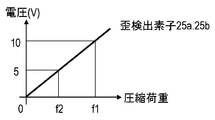
- FIG. 4A shows output voltages of the strain detection elements 25a and 25b when a compression load F is applied to the positions X1 and X2 of the side surface 22b of the casing 22 of the information device of the comparative example.
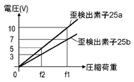
- FIG. 4B shows output voltages of the strain detection elements 25a and 25b when a compressive load F is applied to the positions X1 and X2 of the side surface 22b of the casing 22 of the information device 21 according to the first embodiment.
- the horizontal axis indicates the magnitude of the compression load
- the vertical axis indicates the output voltage of the strain detection element.
- the information device of the comparative example differs from the information device 21 in the first embodiment in that the distances L1 and L2 are the same, that is, outputs the same signal for the same amount of distortion applied to the side surface 22b. That is different.
- the stress concentration portions 26a and 26b the stress concentration portion located at a distance L3 from the position where the compression load F is applied is applied with the compression load f1, and the stress located at a distance 2 ⁇ L3 from the position where the compression load F is applied.
- a compressive load f2 is applied to the concentrated portion.
- the compressive load F when the compressive load F is applied to the position X1, the compressive load f1 is applied to the stress concentration portion 26a, and at the same time, the compressive load f2 is applied to the stress concentration portion 26b. Further, when the compressive load F is applied to the position X2, the compressive load f2 is applied to the stress concentrated portion 26a, and at the same time, the compressive load f1 is applied to the stress concentrated portion 26b.
- 4A shows the output voltage output from the strain detection element 25b with respect to the compression load F of the information device of the comparative example in which the lengths in the thickness direction of the stress concentration portions 26a and 26b are equal to each other and the distances L1 and L2 are the same. Show.
- the information device of the comparative example is different from the information device 21 in the first embodiment in that the distances L1 and L2 are equal.
- the stress concentration portions 26a and 26b have different lengths in the thickness direction, and the distance L1 is different from the distance L2 and specifically smaller than the distance L2. Since the distance L1 is equal to the distance L2 in the information device of the comparative example, the force applied to the strain detection elements 25a and 25b is equal when the compression load F is applied to the side surface 22b, and the strain detection elements 25a and 25b are the same as shown in FIG. 4A. Has output characteristics.
- the amount of strain transmitted to the strain detection element 25a is larger than the amount of strain transmitted to the strain detection element 25b. Therefore, as shown in FIG. 4B, in the information equipment 21, the output characteristics of the strain detection elements 25a and 25b are different.
- the output voltages V1 and V2 of the strain detection elements 25a and 25b when the compression load F is applied to the position X1 are 10V and 5V, respectively.
- the absolute value V of the difference between the output voltages V1 and V2 of the strain detection elements 25a and 25b is 5V.
- the output voltages V1 and V2 of the strain detection elements 25a and 25b when the compression load F is applied to the position X2 are 5V and 10V, respectively, and the output voltage V1 of the strain detection elements 25a and 25b.
- the absolute value V of the difference between V2 is 5V.
- the absolute value V of the difference between the output voltages V1 and V2 of the strain detection elements 25a and 25b becomes the same regardless of the positions X1 and X2 to which the load F is applied, and the compression load F is in any of the positions X1 and X2. It is not possible to determine whether they have joined.
- the output voltages V1 and V2 are 10V and 3V, respectively, and the absolute value V of the difference between the output voltages V1 and V2 of the strain detection elements 25a and 25b is 7V.
- the output voltages V1 and V2 of the strain detection elements 25a and 25b when the compressive load F is applied to the position X2 are 7V and 5V, respectively, and the absolute value of the difference between the output voltages V1 and V2 of the strain detection elements 25a and 25b.
- V becomes 2V.
- the processing circuit 24a determines which position on the side surface 22b the compressive load F is on. It is possible to determine whether it has been added.
- the processing circuit 24a can determine which position of the side surface 22b is applied with the two strain detection elements 25a and 25b, and therefore the information device 21 can downsize the portion where the strain detection elements 25a and 25b are provided.
- the space in the housing 22 can be used effectively.
- the processing circuit 24a Since the finger position can be accurately determined, the processing circuit 24a can perform more advanced control.
- the position information is detected by three or more sensor sheets 215 in order to accurately detect the sliding position, and the size of the device increases. Further, if the number of sensor sheets 215 is reduced in order to reduce the size of the input device 212, it is difficult to accurately detect the sliding position. As described above, in the input device 212 which is a conventional information device, it is difficult to simultaneously realize downsizing and accurate detection of the sliding position, and the accuracy of controlling the function of the information device is poor.
- the stress concentration portions 26a and 26b are in the thickness direction, that is, the stress concentration in the direction from the stress concentration portions 26a and 26b to the strain detection elements 25a and 25b.
- the distances L1 and L2 from the stress concentration portions 26a and 26b to the strain detection elements 25a and 25b are made different.
- the distances L1 and L2 can be made different even if the thicknesses of the strain detection elements 25a and 25b are made different.
- the distances L1 and L2 can be made different by arranging the substrate 24 obliquely with respect to the side surface 22b.
- the stress concentration portions 26a and 26b are provided on the side surface 22b. However, if the stress concentration portions 26a and 26b face the strain detection elements 25a and 25b, respectively, the stress concentration portions 26a and 26b It may be provided on the back surface 22d or the front surface 22a.
- the information apparatus 21 includes two stress concentration portions 26a and 26b and two strain detection elements 25a and 25b, and each includes three or more stress concentration portions and three or more strain detection elements facing each other. May be provided. In this case, if at least two of the strain detection elements have different outputs for the same strain amount, the same effect as that of the information device 21 in the first embodiment can be obtained. The position where the load is applied can be detected with high accuracy. Further, since the outputs of the three or more strain detecting elements with respect to the same strain amount are different from each other, the position where the load is applied can be detected with higher accuracy.
- the stress concentration portions 26a and 26b may mechanically connect the substrate 24 and the side surface 22b. With such a configuration, it is not necessary to directly attach the substrate 24 on which the strain detection elements 25a and 25b are mounted to the casing 22 of the information device 21, so that the design freedom of the information device 21 is increased. Furthermore, since the substrate 24 and the inner surface of the housing 22 are mechanically connected via the stress concentration portions 26a and 26b, the stress concentration portions 26a and 26b can be applied even if the compressive load applied to the housing surface of the information device 21 is small. Since strain is efficiently transmitted to the strain detection elements 25a and 25b via the, a sufficiently large signal is generated from the strain detection elements 25a and 25b.
- the positions where the strain detection elements 25a and 25b are provided may be different from each other in the vertical direction in FIG. 1A, that is, in the height direction of the information device 21. Even in such a configuration, the outputs of the strain detection elements 25a and 25b can be made different with respect to the same strain amount, and the same effect can be obtained. Also, by providing three or more strain detection elements, the information device 21 can detect the position where the compression load F is applied on the side surface 22b with high accuracy.
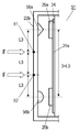
- FIG. 5 is an enlarged cross-sectional view of the information device 51 according to Embodiment 2 of the present invention.
- the information device 51 according to the second embodiment is provided on the side surface 22b of the housing 22 so as to face the strain detection elements 25a and 25b, respectively, instead of the stress concentration portions 26a and 26b of the information device 21 according to the first embodiment.
- Stress concentration portions 56a and 56b are provided.
- the stress concentration portions 56a and 56b have different shapes.
- the stress concentration portion 56a has a conical shape, and the stress concentration portion 56b has a hemispherical shape.
- the stress concentration part 56a has a sharper tip than the stress concentration part 56b, for example, when the user presses the side surface 22b with a finger and applies a compressive load F to the side surface 22b, the stress concentration part 26a is distorted.
- the amount of strain transmitted to the detection element 25a is larger than the amount of strain transmitted from the stress concentration portion 56b to the strain detection element 25b.
- the distance L1 from the stress concentration portion 56a to the strain detection element 25a may be equal to the distance L2 from the stress concentration portion 56b to the strain detection element 25b.
- the amount of strain transmitted from the stress concentration portions 56a and 56b to the strain detection elements 25a and 25b is different. 24a can accurately detect the position of the side surface 22b where the compression load F is applied.
- the stress concentration portion 56a and the stress concentration portion 56b have a conical shape and a hemispherical shape, respectively.
- the stress concentration portions 56a and 56b have a cylindrical shape or a rectangular parallelepiped shape. If they are different, they have the same effect.
- FIG. 6 is an enlarged view of the information device 61 according to Embodiment 3 of the present invention.
- the information device 61 in the third embodiment is provided on the side surface 22b of the housing 22 so as to face the strain detection elements 25a and 25b, respectively, instead of the stress concentration portions 26a and 26b of the information device 21 in the first embodiment. Stress concentration portions 66a and 66b are provided.
- the distance L11 from the center of the strain detection element 25a to the center of the stress concentration portion 66a in the direction parallel to the side surface 22b is from the center of the strain detection element 25b to the center of the stress concentration portion 66b. Is different from the distance L12.
- the centers of the strain detection element 25a and the stress concentration portion 26a coincide with the normal direction of the side surface 22b, but the centers of the strain detection element 25b and the stress concentration portion 66b are the side surfaces.
- a stress concentration portion 66b is provided so as to be shifted in a direction parallel to 22b.
- FIG. 7 shows the sensitivity characteristics of the strain detection elements 25a and 25b with respect to the strain.
- the dark portion is a portion with high distortion amount detection sensitivity.
- the strain detection elements 25a and 25b have the highest strain amount detection sensitivity at the center of the strain detection elements 25a and 25b, and the detection sensitivity of the strain amount decreases concentrically as the distance from the center increases. Therefore, for example, when the user applies a compressive load F to the side surface 22b by pressing the side surface 22b with a finger or the like, as shown in FIG.
- the distance L11 to the center of the detection element 25a is different from the distance L12 from the position where the stress concentration portion 66b contacts the strain detection element 25b to the center of the strain detection element 25b.
- the outputs of the strain detection elements 25a and 25b can be made different. Therefore, the difference in output between the strain detection elements 25a and 25b is not the same at least at two different positions, and the processing circuit 24a can more accurately detect the position where the compression load is applied to the side surface 22b.
- FIG. 8 is an enlarged view of the information device 71 according to Embodiment 4 of the present invention.
- the information device 71 in the fourth embodiment is provided on the side surface 22b of the housing 22 so as to face the strain detection elements 25a and 25b, respectively, instead of the stress concentration portions 26a and 26b of the information device 21 in the first embodiment. Stress concentration portions 76a and 76b are provided.
- the stress concentration portions 76a and 76b have the same thickness, and the distance L1 from the stress concentration portion 76a to the strain detection element 25a and the distance from the stress concentration portion 76b to the strain detection element 25b. L2 is equal.
- the stress concentration portion 76a is made of a resin such as polycarbonate, and the stress concentration portion 76b is made of a metal such as aluminum. As described above, the stress concentration portions 76a and 76b are formed of different materials.
- the stress concentration portion 76a is made of a material having lower rigidity than the stress concentration portion 76b, the amount of strain transmitted from the stress concentration portion 76a to the strain detecting element 25a is the stress concentration portion 76b. Is smaller than the amount of strain transmitted to the strain detecting element 25b. Thereby, the difference between the outputs of the strain detection elements 75a and 75b is not the same at at least two different positions, and the processing circuit 24a can more accurately detect the position where the compression load is applied to the side surface 22b. .
- the stress concentration portion 76a is made of a resin such as polycarbonate and the stress concentration portion 76b is made of a metal such as aluminum.
- the stress concentration portion 76a is made of a combination of resin materials or metal materials having different rigidity. The same effect can be obtained by forming the portions 76a and 76b with materials having different rigidity.
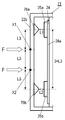
- FIG. 9 is an enlarged view of the information device 81 according to the fifth embodiment of the present invention. 9, the same reference numerals are assigned to the same parts as those of the information equipment 71 in the fourth embodiment shown in FIG.
- the information device 81 in the fifth embodiment includes strain detection elements 85a and 85b and stress concentration portions 86a and 86b instead of the strain detection elements 25a and 25b and the stress concentration portions 76a and 76b of the information device 81 in the fourth embodiment.
- the stress concentration portions 86a and 86b are mounted on the substrate 24, and the stress concentration portion 86a. , 86b are provided on the side surface 22b of the housing 22 so as to face the strain detection elements 85a, 85b, respectively.
- the distance L1 from the strain detection element 85a to the stress concentration portion 86a is the same as the distance L2 from the strain detection element 85b to the stress concentration portion 86b.
- the output characteristics with respect to the strain amounts of the strain detection elements 85a and 85b are different.
- the stress concentration portions 86a and 86b are made of the same material and have the same rigidity.
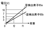
- FIG. 10 shows output characteristics of the strain detection elements 85a and 85b of the information device 81 according to the fifth embodiment. As shown in FIG. 10, the strain detection element 85a has a larger output value when the same strain amount is applied than the strain detection element 85b.
- the strain detection element 85a since the strain detection element 85a has the natural frequencies fa and fb, the beam-shaped vibrating bodies 33 and 43 that constitute the strain detection element, like the strain detection element 25a in the first to fourth embodiments, respectively. It has the same output characteristics as the strain detection element 25a in the first to fourth embodiments.
- the beam-shaped vibrating bodies 33 and 43 of the strain detection element 85b have natural frequencies fa and fc, respectively.
- the natural frequency fc is different from the natural frequency fb.
- the strain detection element 85b has an output characteristic different from that of the strain detection element 85a.
- F When F is applied, the vibration body 33 of the strain detection element 85b extends in the longitudinal direction D33, and the vibration body 43 contracts in the beam-shaped longitudinal direction D43 by a length corresponding to the Poisson's ratio of the side surface 22b of the housing 22. .
- the processing circuit 24 a can measure the load acting on the side surface 22 b of the housing 22 with high sensitivity by taking the difference between the vibration frequency of the vibration body 33 and the vibration frequency of the vibration body 43.
- the outputs of the strain detection elements 85a and 85b when the compressive load F is applied to the side surface 22b are different. Accordingly, the difference in output between the strain detection elements 85a and 85b is not the same at least at two different positions, and the processing circuit 24a can more accurately detect the position where the compression load is applied to the side surface 22b.
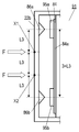
- FIG. 11 is an enlarged view of the information device 91 according to Embodiment 6 of the present invention.
- the information device 91 according to the sixth embodiment includes strain detection elements 95a and 95b, a substrate 84, and a processing circuit 84a instead of the strain detection elements 85a and 85b, the substrate 24, and the processing circuit 24a of the information device 81 according to the fifth embodiment. .
- the strain detection elements 95a and 95b are electrically coupled to a processing circuit 84a having a microcomputer provided on the substrate 84, and the outputs of the strain detection elements 95a and 95b are output by the microcomputer. It is controlled in time. Specifically, the output of the strain detection element 95b is controlled by the microcomputer so that the output is delayed by a predetermined time (10 ms in the sixth embodiment) from the strain detection element 95a. That is, the time from when the strain detecting element 95a receives distortion until the output signal is output to the processing circuit 84a is different from the time from when the strain detecting element 95b receives distortion to when the output signal is output to the processing circuit 84a.
- the strain detection elements 95a and 95b themselves have the same output value with respect to the amount of strain applied to them.
- FIG. 12A shows respective output voltages V1 and V2 of the strain detection elements 95a and 95b when the compressive load F is applied to the position X1 shown in FIG. 11, and FIG. 12B shows the compressive load F applied to the position X2 in FIG.
- the output voltages V1 and V2 of the strain detection elements 95a and 95b are shown. 12A and 12B, the horizontal axis indicates time, and the vertical axis indicates the output voltage of the strain detection elements 95a and 95b.
- the output of the strain detection element 95a is 10V and the output of the strain detection element 95b is 5V.
- the output of the strain detection element 95b is the strain detection.
- the output voltage V2 of the strain detecting element 95b is 4V when the output voltage V1 of 10V is output to the processing circuit 84a of the strain detecting element 95a. Therefore, the output of the strain detecting elements 95a and 95b The absolute value V of the difference between the voltages V1 and V2 is 6V.
- the output voltage V1 of the strain detection element 95a is 5V and the output voltage V2 of the strain detection element 95b is 10V, but as shown in FIG.
- the output voltage V2 of the strain detection element 95b when the strain detection element 95a outputs the output voltage V1 of 5V to the processing circuit 84a is 6V. Therefore, the absolute value V of the difference between the output voltages V1 and V2 of the strain detection elements 95a and 95b is 1V. In this way, by delaying the time when the strain detection element 95b outputs the output voltage V2 to the processing circuit 84a from the time when the strain detection element 95a outputs the output voltage V1 to the processing circuit 84a, the same compression is applied to the positions X1 and X2.
- the processing circuit 84a Since the absolute value V of the difference between the output voltages V1 and V2 of the strain detection elements 95a and 95b when the load F is applied becomes a different value, the processing circuit 84a has a compressive load F between the stress concentration portions 86a and 86b on the side surface 22b. It is possible to more accurately discriminate the position added with.
- the output of the strain detection element 95b is delayed by 10 ms from the output of the strain detection element 95a.
- the delay time is not limited to 10 ms, and the output of the strain detection element 95a is not limited. Is delayed by a predetermined time from the output of the strain detection element 95b, the same effect can be obtained.
- FIG. 13A is a plan view of information device 101 according to Embodiment 7 of the present invention.
- 13B is a cross-sectional view taken along line 13B-13B of information device 101 shown in FIG. 13A.
- the information apparatus 101 according to the seventh embodiment includes strain detection elements 105a and 105b and stress concentration portions 106a and 106b instead of the strain detection elements 95a and 95b and the stress concentration portions 96a and 96b, and supports the substrate 24 and a housing.
- An internal chassis 102 coupled to 22 is further included.
- the strain detection elements 105 a and 105 b are provided on the surface 24 f opposite to the surface 24 e of the substrate 24 facing the side surface 22 b of the housing 22.
- the stress concentration portions 106 a and 106 b bend the substrate 24 by a load applied to the side surface 22 b of the housing 22.
- the strain detection elements 105 a and 105 b detect the bending of the substrate 24.
- the stress concentration portions 106a and 106b transmit the strain on the side surface 22b of the housing 22 to the strain detection elements 105a and 105b via the substrate 24, respectively.
- the internal chassis 102 cantilever-supports the substrate 24. That is, the substrate 24 has an end 24 d supported by the internal chassis 102 and coupled to the housing 22, and an end 24 c located on the opposite side of the end 24 d and not coupled to the housing 22.
- the strain detection elements 105a and 105b themselves have the same output value with respect to the amount of strain applied to them.
- the processing circuit 24a does not temporally control the outputs of the strain detection elements 105a and 105b. Even if thermal stress is applied to the substrate 24 due to the difference in thermal expansion coefficient between the internal chassis 102 and the substrate 24, no output signal is generated from the strain detection elements 105 a and 105 b, and the processing circuit 24 a is used for the housing of the information device 101. It is possible to accurately detect the compressive load applied to the surface 22.
- the substrate 24 is cantilevered at the end 24d, and the strain detection element 105a is closer to the internal chassis 102 than the strain detection element 105b, the same amount of compressive load is applied to the strain detection elements 105a and 106b from the stress concentration portions 106a and 106b.
- the distortions transmitted when F is applied are different from each other, and the processing circuit 24a can accurately detect the position where the compression load F is applied to the side surface 22b.
- FIG. 14A is a plan view of information device 111 according to Embodiment 8 of the present invention.
- 14B is a cross-sectional view taken along line 14B-14B of information device 111 shown in FIG. 14B.
- the information apparatus 111 according to the eighth embodiment includes strain detection elements 115a and 115b, stress concentration portions 116a and 116b, and a substrate 114 instead of the strain detection elements 105a and 105b, the stress concentration portions 106a and 106b, and the substrate 24.
- the substrate 114 extends substantially at right angles to the side surface 22b of the housing 22. That is, the substrate 114 has a main surface 114a that extends substantially perpendicular to the side surface 22b, a back surface 114c opposite to the main surface 114a, and a side end surface that connects the main surface 114a and the back surface 114c between the main surface 114a and the back surface 114c. 114b.
- the substrate 114 has a slit 112 extending from the main surface 114a through the back surface 114c and extending substantially parallel to the side end surface 114b.
- the strain detection elements 115 a and 115 b are provided on the main surface 114 a of the substrate 114 and between the side end surface 114 b of the substrate 114 and the slit 112. Due to the load F applied to the side surface 22b of the housing 22, the stress concentrating portions 116a and 116b push the side end surface 114b of the substrate 114, so that the portion between the side end surface 114b of the substrate 114 and the slit 112 becomes the main surface 114a (back surface 114c). ) In a direction parallel to. The strain detection elements 115a and 115b provided on this portion of the substrate 114 detect the deflection of this portion.
- the stress concentration portions 116a and 116b transmit the strain on the side surface 22b of the housing 22 to the strain detection elements 115a and 115b through this portion of the substrate 114, respectively.
- the substrate 114 on which the strain detection elements 115a and 115b are mounted is easily bent, even if the compressive load F applied to the side surface 22b of the casing 22 of the information device 111 is small, the stress is transmitted from the stress concentration portions 116a and 116b. Due to the distortion, a sufficiently large signal is generated from the strain detection elements 115a and 115b, and the processing circuit 24a can detect the position where the load F is applied on the side surface 22b with high accuracy, and control the function of the information device 111 with higher accuracy. it can.
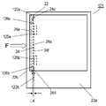
- FIG. 15 is an enlarged view of the information device 121 according to Embodiment 9 of the present invention.
- the information device 121 according to the ninth embodiment includes stress concentration portions 126a and 126b instead of the stress concentration portions 106a and 106b, and includes internal chassis 122a and 122b instead of the internal chassis 102.
- the ends 24c and 24d of the substrate 24 are supported on the printed circuit board by the internal chassis 122a and 122b, respectively, and are coupled to the housing 22.
- the stress concentration portions 126a and 126b abut against the surface 24e of the substrate 24, and the strain detection elements 125a and 125b are not provided with the stress concentration portions 126a and 126b of the substrate 24 but are provided on the surface 24f opposite to the surface 24e. ing.
- the stress concentration portions 126a and 126b transmit the strain on the side surface 22b to the strain detection elements 125a and 125b via the substrate 24, respectively.
- the stress concentration portion 126a is in contact with the surface 24e of the substrate 24 between the strain detection element 125a and the internal chassis 122a (end 24c of the substrate 24), and the stress concentration portion 126b is connected to the strain detection element 125b and the internal chassis 122b (end of the substrate 24). 24d) is in contact with the surface 24e of the substrate 24. Further, as shown in FIG. 15, the substrate 24 is urged by the stress concentration portions 126a and 126b, and is attached with a bias by a distance L4.
- the substrate 24 By being attached with a bias, the substrate 24 is surely brought into contact with the stress concentration portions 126a and 126b, so that the strain on the side surface 22b is easily transmitted from the stress concentration portions 126a and 126b to the strain detection elements 125a and 125b, respectively.
- the stress detection portions 125a and 126b can be surely connected to the strain detection elements 125a and 125b even if there is an influence of manufacturing variations. Distortion can be transmitted to the information device 121, and the productivity of the information device 121 can be improved.
- FIG. 16A is an enlarged view of the information device 121 according to the ninth embodiment, and shows strain transmitted to the strain detection element 125a by the stress concentration unit 126a.
- the distortion occurs on the side surface 22b of the housing 22, the distortion is transmitted to the substrate 24 by the stress concentration portion 126a, and the substrate 24 is deformed. Since the stress concentration portion 126a is provided between the strain detection element 125a and the internal chassis 122a, the portion of the substrate 24 where the strain detection element 125a is provided has the largest curvature. Therefore, compared to the case where the strain detecting element 125a faces the stress concentration portion 126a via the substrate 24, the amount of strain transmitted to the strain detecting element 125a is increased, so that the strain detection accuracy of the processing circuit 24a is increased. Can do.
- the distance from the stress concentration portion 126a to the strain detection element 125a is the distance from the stress concentration portion 126b to the strain detection element 125b in the direction along the surface 24e (24f) of the substrate 24. Is equal to The same effect can be obtained even if the distance from the stress concentration portion 126a to the strain detection element 125a is different from the distance from the stress concentration portion 126b to the strain detection element 125b in the direction along the surface 24e (24f) of the substrate 24. Can do.
- the stress concentration portion 126a is in contact with the substrate 24 between the strain detection element 125a and the internal chassis 122a, and the stress concentration portion 126b is between the strain detection element 125b and the internal chassis 122b. It is in contact with the substrate 24.
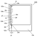
- FIG. 16B is an enlarged view of another information device 121A according to Embodiment 9. In FIG. 16B, the same parts as those of the information equipment 121 shown in FIG. In the information device 121A shown in FIG. 16B, the stress concentration portions 126a and 126b are in contact with the substrate 24 between the strain detection elements 125a and 125b.
- the processing circuit 24a can detect the strain with high accuracy. Similar effects can be obtained.
- the stress concentration portion 126a is in contact with the substrate 24 between the strain detection element 125a and the internal chassis 122a as compared with the information equipment in which the stress concentration portions 126a and 126b are in contact with the substrate 24 between the strain detection elements 125a and 125b.
- the information device 121 in which the stress concentration portion 126b is in contact with the substrate 24 between the strain detection element 125b and the internal chassis 122b transmits to the strain detection elements 125a and 125b regardless of the positions of the stress concentration portions 126a and 126b. Since the amount of distortion becomes more constant and the requirement for accuracy at the time of mounting becomes lower, the productivity of the information device 121 is improved.
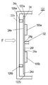
- FIG. 17 is an enlarged view of the information device 131 according to the tenth embodiment of the present invention.
- the information device 131 according to the tenth embodiment further includes an internal chassis 132 fixed to the printed circuit board so as to support the circuit board 24 at the center supported portion 24p between the strain detection elements 125a and 125b.
- the internal chassis 132 is coupled to the housing 22 via a printed board.
- the substrate 24 is supported with respect to the housing 22 by the supported portion 24p.
- the end 24d of the substrate 24 is closer to the strain detection element 125b than the strain detection element 125a.
- the end 24c is located on the opposite side of the end 24d.
- the stress concentration portion 126a is positioned between and in contact with the substrate 24 between the strain detection element 125a and the end 24c of the substrate 24, and the stress concentration portion 126b is positioned between the strain detection element 125b and the end 24d of the substrate 24. 24.
- the ends 24c and 24d of the substrate 24 are fixed by the internal chassis 122a and 122b, respectively.
- the internal chassis 132 contacts the supported portion 24p of the substrate 24 between the strain detection elements 125a and 125b, and supports the substrate 24 so that the substrate 24 is not bent by the supported portion 24p.
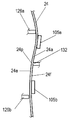
- FIG. 18 is an enlarged view of the information device 131 according to the tenth embodiment, and shows the distortion transmitted to the substrate 24 when the compressive load F is applied to the side surface 22b of the housing 22.
- FIG. 18 when a load F toward the inside of the housing 22 is applied in the vicinity of the stress concentration portion 126a on the side surface 22b of the housing 22, the stress concentration portion 126a out of the stress concentration portions 126a and 126b.
- the substrate 24 is pushed only, the substrate 24 is curved between the end 24c of the substrate 24 and the supported portion 24p of the substrate 24, so that the supported portion of the substrate 24 is the same as the information device 121 in the ninth embodiment.
- the substrate 24 bends with a larger curvature than when 24p is not supported.
- the information device 131 in the tenth embodiment has a larger difference in the output of the strain detection elements 125a and 125b with respect to the same amount of compression load F and is added to the information device 131.
- the detection sensitivity of the compression load F can be improved.
- 200 gf of compressive load of 200 gf was applied to the information device 131 in the tenth embodiment and measured, the difference in output between the strain detection elements 125 a and 125 b was larger than that of the information device not supporting the supported portion 24 p of the substrate 24. It was confirmed that it increased by about 14%.
- both ends 24c and 24d of the substrate 24 are fixed by the internal chassis 122a and 122b.
- the information device 131 may have a cantilever support structure in which only one of the ends 24c and 24d of the substrate 24 is fixed by the internal chassis, and the same effect can be obtained.
- the output of either one of the strain detection elements 125a and 125b is equal to the output at the both ends support, and the other output is equal to the output at the cantilever support.
- the processing circuit 24a can accurately determine the position where the compression load F is applied to the side surface 22b.
- positions such as “front surface”, “back surface”, “side surface”, “side end surface”, “back surface”, and the like depend only on the relative positional relationship of components of information equipment such as a housing and a substrate. It indicates a relative direction and does not indicate an absolute direction such as a vertical direction.
- the information device detects a user input with high accuracy and allows the user to easily operate various functions. Therefore, a digital camera, a notebook PC, a portable game machine, a cellular phone, a portable information terminal ( PDA), smartphones and the like are particularly useful.
Landscapes
- Engineering & Computer Science (AREA)
- General Engineering & Computer Science (AREA)
- Theoretical Computer Science (AREA)
- Human Computer Interaction (AREA)
- Physics & Mathematics (AREA)
- General Physics & Mathematics (AREA)
- Signal Processing (AREA)
- Force Measurement Appropriate To Specific Purposes (AREA)
- Investigating Strength Of Materials By Application Of Mechanical Stress (AREA)
- User Interface Of Digital Computer (AREA)
- Telephone Set Structure (AREA)
- Position Input By Displaying (AREA)
Abstract
Priority Applications (3)
| Application Number | Priority Date | Filing Date | Title |
|---|---|---|---|
| JP2014520962A JPWO2013190850A1 (ja) | 2012-06-22 | 2013-06-21 | 情報機器 |
| CN201380032846.7A CN104412568B (zh) | 2012-06-22 | 2013-06-21 | 信息设备 |
| US14/398,955 US9250737B2 (en) | 2012-06-22 | 2013-06-21 | Information apparatus |
Applications Claiming Priority (4)
| Application Number | Priority Date | Filing Date | Title |
|---|---|---|---|
| JP2012-140505 | 2012-06-22 | ||
| JP2012140505A JP2013102416A (ja) | 2011-10-14 | 2012-06-22 | 携帯情報機器 |
| JP2012215894 | 2012-09-28 | ||
| JP2012-215894 | 2012-09-28 |
Publications (1)
| Publication Number | Publication Date |
|---|---|
| WO2013190850A1 true WO2013190850A1 (fr) | 2013-12-27 |
Family
ID=49768461
Family Applications (1)
| Application Number | Title | Priority Date | Filing Date |
|---|---|---|---|
| PCT/JP2013/003886 Ceased WO2013190850A1 (fr) | 2012-06-22 | 2013-06-21 | Appareil d'informations |
Country Status (4)
| Country | Link |
|---|---|
| US (1) | US9250737B2 (fr) |
| JP (1) | JPWO2013190850A1 (fr) |
| CN (1) | CN104412568B (fr) |
| WO (1) | WO2013190850A1 (fr) |
Families Citing this family (5)
| Publication number | Priority date | Publication date | Assignee | Title |
|---|---|---|---|---|
| KR20190027553A (ko) * | 2017-09-07 | 2019-03-15 | 주식회사 하이딥 | 측면에 터치 압력 감지부를 구비한 휴대용 단말기 |
| CN110209303B (zh) * | 2019-05-31 | 2021-07-16 | 联想(北京)有限公司 | 电子设备和控制方法 |
| US10999421B1 (en) | 2019-12-17 | 2021-05-04 | Robert Bosch Gmbh | System and method for utilizing pressure sensors in an electric device |
| US10812639B1 (en) | 2019-12-17 | 2020-10-20 | Robert Bosch Gmbh | Pressure chamber and associated pressure sensors for a mobile communication device |
| JP7462269B2 (ja) * | 2020-05-19 | 2024-04-05 | パナソニックIpマネジメント株式会社 | 半導体装置及び半導体装置の製造方法 |
Citations (3)
| Publication number | Priority date | Publication date | Assignee | Title |
|---|---|---|---|---|
| JP2006018505A (ja) * | 2004-06-30 | 2006-01-19 | Ntt Docomo Inc | 携帯端末 |
| EP2175344A2 (fr) * | 2008-10-06 | 2010-04-14 | Samsung Electronics Co., Ltd. | Procédé et appareil pour afficher une interface graphique utilisateur en fonction d'un motif de contact de l'utilisateur |
| JP2011164042A (ja) * | 2010-02-15 | 2011-08-25 | Panasonic Corp | 物理量センサ |
Family Cites Families (10)
| Publication number | Priority date | Publication date | Assignee | Title |
|---|---|---|---|---|
| JP2001069223A (ja) | 1999-08-27 | 2001-03-16 | Matsushita Electric Ind Co Ltd | 通信装置 |
| JP2004274494A (ja) * | 2003-03-10 | 2004-09-30 | Mitsubishi Electric Corp | 携帯情報端末 |
| JP5710859B2 (ja) * | 2007-09-21 | 2015-04-30 | ソニー株式会社 | 入力装置及び電子機器 |
| US8264463B2 (en) * | 2007-09-21 | 2012-09-11 | Sony Corporation | Input device and electronic apparatus |
| JP2009217804A (ja) | 2007-09-21 | 2009-09-24 | Sony Corp | 入力装置及び電子機器 |
| JP2009136848A (ja) | 2007-12-11 | 2009-06-25 | Furukawa Sky Kk | 放熱塗装金属板 |
| JP2010108891A (ja) | 2007-12-27 | 2010-05-13 | Jfe Steel Corp | ディスプレイ装置 |
| JP2010117842A (ja) | 2008-11-12 | 2010-05-27 | Sharp Corp | 携帯情報端末 |
| CN101923417B (zh) * | 2009-06-10 | 2013-06-05 | 鸿富锦精密工业(深圳)有限公司 | 触控式输入装置 |
| JP2012109508A (ja) | 2010-10-29 | 2012-06-07 | Jnc Corp | 電子デバイス用放熱部材、電子デバイスおよび製造方法 |
-
2013
- 2013-06-21 WO PCT/JP2013/003886 patent/WO2013190850A1/fr not_active Ceased
- 2013-06-21 CN CN201380032846.7A patent/CN104412568B/zh not_active Expired - Fee Related
- 2013-06-21 JP JP2014520962A patent/JPWO2013190850A1/ja not_active Ceased
- 2013-06-21 US US14/398,955 patent/US9250737B2/en not_active Expired - Fee Related
Patent Citations (3)
| Publication number | Priority date | Publication date | Assignee | Title |
|---|---|---|---|---|
| JP2006018505A (ja) * | 2004-06-30 | 2006-01-19 | Ntt Docomo Inc | 携帯端末 |
| EP2175344A2 (fr) * | 2008-10-06 | 2010-04-14 | Samsung Electronics Co., Ltd. | Procédé et appareil pour afficher une interface graphique utilisateur en fonction d'un motif de contact de l'utilisateur |
| JP2011164042A (ja) * | 2010-02-15 | 2011-08-25 | Panasonic Corp | 物理量センサ |
Also Published As
| Publication number | Publication date |
|---|---|
| US20150138106A1 (en) | 2015-05-21 |
| CN104412568A (zh) | 2015-03-11 |
| US9250737B2 (en) | 2016-02-02 |
| JPWO2013190850A1 (ja) | 2016-02-08 |
| CN104412568B (zh) | 2017-04-05 |
Similar Documents
| Publication | Publication Date | Title |
|---|---|---|
| CN102539022B (zh) | 检测装置、电子设备以及机械手 | |
| JP5570640B2 (ja) | 圧電素子および電子機器 | |
| CN205910637U (zh) | 电子设备及剪切力传感器 | |
| CN101341605B (zh) | 用于组合式压力传感器和致动器的经济元件及其操作方法 | |
| US20070080951A1 (en) | Input device and electronic device using the input device | |
| WO2012053202A1 (fr) | Dispositif d'écran tactile | |
| CN216719076U (zh) | 触控板、压力触控装置和电子设备 | |
| CN104412568B (zh) | 信息设备 | |
| CN112445329A (zh) | 触控反馈模组及触控装置 | |
| WO2016035628A1 (fr) | Dispositif vibratoire | |
| KR20170030023A (ko) | 이동 단말기 | |
| KR102520107B1 (ko) | 전자 기기 및 이의 구동 방법 | |
| JP6335626B2 (ja) | 触感伝達装置 | |
| JP2013205952A (ja) | パネル装置 | |
| US9348442B2 (en) | Input apparatus | |
| CN114761144A (zh) | 振动装置 | |
| JP2013020362A (ja) | 入力装置、表示装置、および機器 | |
| JP2013102413A (ja) | 携帯情報機器 | |
| WO2025118257A1 (fr) | Transducteur piézoélectrique et touche de détection de pression | |
| WO2015098061A1 (fr) | Instrument électronique | |
| JP5921811B2 (ja) | 電子機器 | |
| JP2015138369A (ja) | 電子機器 | |
| KR101154363B1 (ko) | 진동 엑츄에이터 모듈 | |
| JP2013167939A (ja) | 静電容量式入力装置 | |
| JP2015152385A (ja) | 電子機器 |
Legal Events
| Date | Code | Title | Description |
|---|---|---|---|
| 121 | Ep: the epo has been informed by wipo that ep was designated in this application |
Ref document number: 13806460 Country of ref document: EP Kind code of ref document: A1 |
|
| ENP | Entry into the national phase |
Ref document number: 2014520962 Country of ref document: JP Kind code of ref document: A |
|
| WWE | Wipo information: entry into national phase |
Ref document number: 14398955 Country of ref document: US |
|
| NENP | Non-entry into the national phase |
Ref country code: DE |
|
| 122 | Ep: pct application non-entry in european phase |
Ref document number: 13806460 Country of ref document: EP Kind code of ref document: A1 |